ICGOO在线商城 > 500DDAB-ACF
 Datasheet下载
- 型号: 500DDAB-ACF
- 制造商: Silicon Laboratories
- 库位|库存: xxxx|xxxx
- 要求:
| 数量阶梯 | 香港交货 | 国内含税 |
| +xxxx | $xxxx | ¥xxxx |
查看当月历史价格
查看今年历史价格
500DDAB-ACF产品简介:
ICGOO电子元器件商城为您提供500DDAB-ACF由Silicon Laboratories设计生产,在icgoo商城现货销售,并且可以通过原厂、代理商等渠道进行代购。 提供500DDAB-ACF价格参考以及Silicon Laboratories500DDAB-ACF封装/规格参数等产品信息。 你可以下载500DDAB-ACF参考资料、Datasheet数据手册功能说明书, 资料中有500DDAB-ACF详细功能的应用电路图电压和使用方法及教程。
| 参数 | 数值 |
| 产品目录 | 晶体和振荡器 |
| 描述 | OSC PROG HCSL 3.3V 150PPM SMD |
| 产品分类 | |
| 品牌 | Silicon Laboratories Inc |
| 数据手册 | |
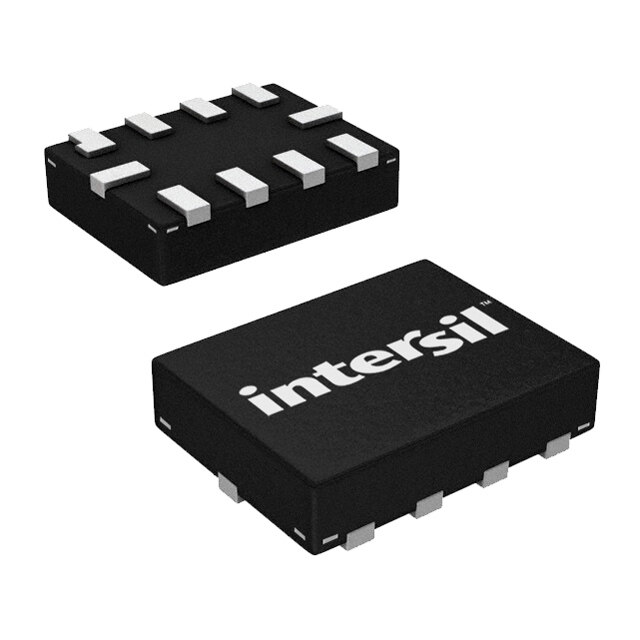
| 产品图片 |
|
| 产品型号 | 500DDAB-ACF |
| rohs | 无铅 / 符合限制有害物质指令(RoHS)规范要求 |
| 产品系列 | Si500D |
| 产品培训模块 | http://www.digikey.cn/PTM/IndividualPTM.page?site=cn&lang=zhs&ptm=30044 |
| 产品目录页面 | |
| 其它名称 | 500DDAB-ACFR |
| 功能 | 三态(输出启用) |
| 包装 | 管件 |
| 可用频率范围 | 900kHz ~ 200MHz |
| 大小/尺寸 | 0.157" 长 x 0.126" 宽(4.00mm x 3.20mm) |
| 安装类型 | 表面贴装 |
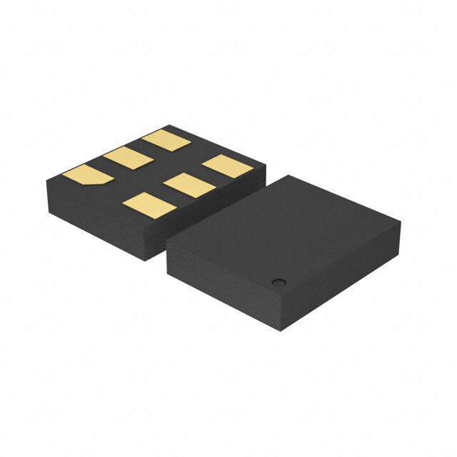
| 封装/外壳 | 6-SMD,无引线(DFN,LCC) |
| 工作温度 | 0°C ~ 70°C |
| 扩频带宽 | - |
| 标准包装 | 100 |
| 特色产品 | http://www.digikey.com/cn/zh/ph/SiLabs/Si500.html |
| 电压-电源 | 3.3V |
| 电流-电源(最大值) | 29.3mA |
| 电流-电源(禁用)(最大值) | 10.7mA |
| 类型 | 由 Digi-Key 编程(请在网站订购单中输入您需要的频率) |
| 输出 | HCSL |
| 频率稳定度 | ±150ppm |
| 高度 | 0.035"(0.90mm) |


.jpg)

- 商务部:美国ITC正式对集成电路等产品启动337调查
- 曝三星4nm工艺存在良率问题 高通将骁龙8 Gen1或转产台积电
- 太阳诱电将投资9.5亿元在常州建新厂生产MLCC 预计2023年完工
- 英特尔发布欧洲新工厂建设计划 深化IDM 2.0 战略
- 台积电先进制程称霸业界 有大客户加持明年业绩稳了
- 达到5530亿美元!SIA预计今年全球半导体销售额将创下新高
- 英特尔拟将自动驾驶子公司Mobileye上市 估值或超500亿美元
- 三星加码芯片和SET,合并消费电子和移动部门,撤换高东真等 CEO
- 三星电子宣布重大人事变动 还合并消费电子和移动部门
- 海关总署:前11个月进口集成电路产品价值2.52万亿元 增长14.8%


PDF Datasheet 数据手册内容提取
Si500D DIFFERENTIAL OUTPUT SILICON OSCILLATOR Features Quartz-free, MEMS-free, and PLL-free all-silicon Footprint compatible with industry- oscillator standard 3.2x5.0mm XOs Any output frequencies from 0.9 to 200MHz CMOS, SSTL, LVPECL, LVDS, and HCSL Short lead times versions available Excellent temperature stability (±20ppm) Driver stopped, tri-state, or powerdown Highly reliable startup and operation operation High immunity to shock and vibration RoHS compliant Low jitter: <1.5ps rms 1.8, 2.5, or 3.3V options 0 to 85°C operation includes 10-year aging in hot Low power environments More than 10x better fit rate than competing crystal solutions Specifications Parameters Condition Min Typ Max Units Frequency Range 0.9 — 200 MHz Temperature stability, — ±10 — ppm 0 to +70°C Temperature stability, — ±20 — ppm 0 to +85°C Frequency Stability Total stability, — — ±150 ppm 0 to +70°C operation1 Total stability, — — ±250 ppm 0 to +85°C operation2 Commercial 0 — 70 °C Operating Temperature Extended commercial 0 — 85 °C Storage Temperature –55 — +125 °C 1.8V option 1.71 — 1.98 V Supply Voltage 2.5V option 2.25 — 2.75 V 3.3V option 2.97 — 3.63 V Notes: 1. Inclusive of 25°C initial frequency accuracy, operating temperature range, supply voltage change, output load change, first-year aging at 25°C, shock, vibration, and one solder reflow. 2. Inclusive of 25°C initial frequency accuracy, operating temperature range, supply voltage change, output load change, ten-year aging at 85°C, shock, vibration, and one solder reflow. 3. See “AN409: Output Termination Options for the Si500S and Si500D Silicon Oscillators” for further details regarding output clock termination recommendations. 4. V = .5 x V . TT DD 5. V = .45 x V . TT DD Rev. 1.1 10/11 Copyright © 2011 by Silicon Laboratories Si500D
Si500D Parameters Condition Min Typ Max Units LVPECL — 34.0 36.0 mA Low Power LVPECL — 19.3 22.2 mA LVDS — 14.9 16.5 mA HCSL — 25.3 29.3 mA Differential CMOS(3.3V option, — 33 36 mA 10pF on each output, 200MHz) Supply Current Differential CMOS(3.3V option, — 16 — mA 1pFon each output, 40MHz) Differential SSTL-3.3 — 24.5 27.7 mA Differential SSTL-2.5 — 24.3 26.7 mA Differential SSTL-1.8 — 22.2 25 mA Tri-State — 9.7 10.7 mA Powerdown — 1.0 1.9 mA Output Symmetry V =0 46 – 13ns/T — 54 + 13ns/T % DIFF CLK CLK LVPECL/LVDS — — 460 ps Rise and Fall Times (20/80%)3 HCSL/Differential SSTL — — 800 ps Differential CMOS, 15pF, >80MHz — 1.1 1.6 ns LVPECL Output Option Mid-level VDD – 1.5 — VDD – 1.34 V (DC coupling, 50 to VDD – 2.0V)3 Diff swing .720 — .880 VPK Low Power LVPECL Output Option Mid-level — N/A — V (AC coupling, 100 Differential Load)3 Diff swing .68 — .95 VPK LVDS Output Option (2.5/3.3V) Mid-level 1.15 — 1.26 V (RTERM=100 diff)3 Diff swing 0.25 — 0.45 VPK LVDS Output Option (1.8V) Mid-level 0.85 — 0.96 V (RTERM=100 diff)3 Diff swing 0.25 — 0.45 VPK Mid-level 0.35 — 0.425 V HCSL Output Option3 Diff swing 0.65 — 0.82 V PK DC termination per pad 45 — 55 V , sourcing 9mA V –0.6 — — V CMOS Output Voltage3 OH DD V , sinking 9mA — — 0.6 V OL V V + 0.375 — — SSTL-1.8 Output Voltage4 OH TT V V — — V – 0.375 OL TT V V + 0.48 — — SSTL-2.5 Output Voltage4 OH TT V V — — V – 0.48 OL TT V V + 0.48 — — SSTL-3.3 Output Voltage5 OH TT V V — — V – 0.48 OL TT From time V crosses min spec Powerup Time DD — — 2 ms supply OE Deassertion to Clk Stop — — 250 + 3xT ns CLK Return from Output Driver Stopped — — 250 + 3xT ns Mode CLK Return From Tri-State Time — — 12 + 3xT µs CLK Notes: 1. Inclusive of 25°C initial frequency accuracy, operating temperature range, supply voltage change, output load change, first-year aging at 25°C, shock, vibration, and one solder reflow. 2. Inclusive of 25°C initial frequency accuracy, operating temperature range, supply voltage change, output load change, ten-year aging at 85°C, shock, vibration, and one solder reflow. 3. See “AN409: Output Termination Options for the Si500S and Si500D Silicon Oscillators” for further details regarding output clock termination recommendations. 4. V = .5 x V . TT DD 5. V = .45 x V . TT DD 2 Rev. 1.1
Si500D Parameters Condition Min Typ Max Units Return From Powerdown Time — — 2 ms ps Non-CMOS — 1 2 RMS Period Jitter (1-sigma) ps CMOS, C =7pF — 1 3 L RMS 1.0MHz – min(20MHz, ps — 0.6 1 0.4xF ),non-CMOS RMS Integrated Phase Jitter OUT 1.0MHz – min(20MHz, ps — 0.7 1.5 0.4xF ),CMOS format RMS OUT Notes: 1. Inclusive of 25°C initial frequency accuracy, operating temperature range, supply voltage change, output load change, first-year aging at 25°C, shock, vibration, and one solder reflow. 2. Inclusive of 25°C initial frequency accuracy, operating temperature range, supply voltage change, output load change, ten-year aging at 85°C, shock, vibration, and one solder reflow. 3. See “AN409: Output Termination Options for the Si500S and Si500D Silicon Oscillators” for further details regarding output clock termination recommendations. 4. V = .5 x V . TT DD 5. V = .45 x V . TT DD Rev. 1.1 3
Si500D Package Specifications Table 1. Package Diagram Dimensions (mm) Dimension Min Nom Max Dimension Min Nom Max A 0.80 0.85 0.90 L1 0.00 0.05 0.10 A1 0.00 0.03 0.05 aaa — — 0.10 b 0.59 0.64 0.69 bbb — — 0.10 D 3.20 BSC. ccc — — 0.08 e 1.27 BSC. ddd — — 0.10 E 4.00 BSC. eee — — 0.05 L 0.95 1.00 1.05 Table 2. Pad Connections Table 3. Tri-State/Powerdown/Driver Stopped Function on OE (3rd Option Code) 1 OE NC—Make no external A B C D E F 2 connection to this pin Open Active Active Active Active Active Active 3 GND 1 Tri- Power- Driver Active Active Active Level State down Stopped 4 Output 5 Complementary Output 0 Tri- Active Power- Active Driver Active Level State down Stopped 6 VDD 0 C CC CC T T T T T T Dimension (mm) C1 2.70 E 1.27 Y YWW X1 0.75 Y1 1.55 0 = Si500 CCCCC = mark code TTTTTT = assembly manufacturing code YY = year WW = work week Figure 1. Recommended Land Pattern Figure 2. Top Mark 4 Rev. 1.1
Si500D Environmental Compliance Parameter Conditions/Test Method Mechanical Shock MIL-STD-883, Method 2002.4 Mechanical Vibration MIL-STD-883, Method 2007.3 A Resistance to Soldering Heat MIL-STD-202, 260C° for 8 seconds Solderability MIL-STD-883, Method 2003.8 Damp Heat IEC 68-2-3 Moisture Sensitivity Level J-STD-020, MSL 3 Ordering Information The Si500D supports a variety of options including frequency, output format, supply voltage, and tri- state/powerdown. Specific device configurations are programmed into the Si500D at time of shipment. Configurations are specified using the figure below. Silicon Labs provides a web-based part number utility that can be used to simplify part number configuration. Refer to www.silabs.com/SiliconXOPartnumber to access this tool. The Si500D XO series is supplied in a ROHS-compliant, Pb-free, 6-pad, 3.2 x 4.0mm package. Tape and reel packaging is available as an ordering option. 500D X X X XXMXXXX A C X R Si500 Frequency R = Tape & Reel Differential xMxxxxx: f < 10 MHz Blank = Cut-Tape Oscillator OUT xxMxxxx: 10 MHz < f < 100 MHz OUT xxxMxxx: f > 100 MHz OUT 1st Option Code V Format DD 3rd Option Code Oper. Temp Range A 3.3 LVPECL Tri-State/Powerdown/ F 0 to 70 °C B 3.3 Low Power LVPECL Output Driver Stopped *H 0 to 85 °C C 3.3 LVDS A OE active high/tristate D 3.3 HCSL B OE active low/tristate E 3.3 Dual Output CMOS C OE active high/powerdown F 3.3 Differential CMOS D OE active low/powerdown Product Revision = C G 3.3 Dual Output SSTL E OE active high/driver stopped H 3.3 Differential SSTL F OE active low/driver stopped J 2.5 LVPECL K 2.5 Low Power LVPECL 2nd Option Code Package L 2.5 LVDS M 2.5 HCSL Stability (ppm, max) A 3.2 x 4.0 mm SMD N 2.5 Dual Output CMOS A ±150 P 2.5 Differential CMOS B ±250 Q 2.5 Dual Output SSTL R 2.5 Differential SSTL S 1.8 LVDS T 1.8 HCSL U 1.8 Dual Output CMOS V 1.8 Differential CMOS *Note: Only +250 ppm is supported. W 1.8 Dual Output SSTL X 1.8 Differential SSTL Rev. 1.1 5
Si500D DOCUMENT CHANGE LIST Revision 0.2 to Revision 0.3 Revision B to Revision C updated in Ordering Information 0 to 85C° Operating Temperature Range option added Revision 0.3 to Revision 1.0 Clarified SSTL specifications. Revised Differential CMOS supply current values. Clarified Differential CMOS supply current loading conditions. Revision 1.0 to Revision 1.1 Updated Ordering information for ±250ppm from 0 to +85°C. Updated jitter from 1.5ps to 1.5ps rms. Updated operating temperature to include extended commercial at 0 to +85°C. Updated features to include LVPECL, LVDS, and HCSL. 6 Rev. 1.1
ClockBuilder Pro One-click access to Timing tools, documentation, software, source code libraries & more. Available for Windows and iOS (CBGo only). www.silabs.com/CBPro Timing Portfolio SW/HW Quality Support and Community www.silabs.com/timing www.silabs.com/CBPro www.silabs.com/quality community.silabs.com Disclaimer Silicon Labs intends to provide customers with the latest, accurate, and in-depth documentation of all peripherals and modules available for system and software implementers using or intending to use the Silicon Labs products. Characterization data, available modules and peripherals, memory sizes and memory addresses refer to each specific device, and "Typical" parameters provided can and do vary in different applications. Application examples described herein are for illustrative purposes only. Silicon Labs reserves the right to make changes without further notice to the product information, specifications, and descriptions herein, and does not give warranties as to the accuracy or completeness of the included information. Without prior notification, Silicon Labs may update product firmware during the manufacturing process for security or reliability reasons. Such changes will not alter the specifications or the performance of the product. Silicon Labs shall have no liability for the consequences of use of the information supplied in this document. This document does not imply or expressly grant any license to design or fabricate any integrated circuits. The products are not designed or authorized to be used within any FDA Class III devices, applications for which FDA premarket approval is required or Life Support Systems without the specific written consent of Silicon Labs. A "Life Support System" is any product or system intended to support or sustain life and/or health, which, if it fails, can be reasonably expected to result in significant personal injury or death. Silicon Labs products are not designed or authorized for military applications. Silicon Labs products shall under no circumstances be used in weapons of mass destruction including (but not limited to) nuclear, biological or chemical weapons, or missiles capable of delivering such weapons. Silicon Labs disclaims all express and implied warranties and shall not be responsible or liable for any injuries or damages related to use of a Silicon Labs product in such unauthorized applications. Trademark Information Silicon Laboratories Inc.® , Silicon Laboratories®, Silicon Labs®, SiLabs® and the Silicon Labs logo®, Bluegiga®, Bluegiga Logo®, ClockBuilder®, CMEMS®, DSPLL®, EFM®, EFM32®, EFR, Ember®, Energy Micro, Energy Micro logo and combinations thereof, "the world’s most energy friendly microcontrollers", Ember®, EZLink®, EZRadio®, EZRadioPRO®, Gecko®, Gecko OS, Gecko OS Studio, ISOmodem®, Precision32®, ProSLIC®, Simplicity Studio®, SiPHY®, Telegesis, the Telegesis Logo®, USBXpress® , Zentri, the Zentri logo and Zentri DMS, Z-Wave®, and others are trademarks or registered trademarks of Silicon Labs. ARM, CORTEX, Cortex-M3 and THUMB are trademarks or registered trademarks of ARM Holdings. Keil is a registered trademark of ARM Limited. Wi-Fi is a registered trademark of the Wi-Fi Alliance. All other products or brand names mentioned herein are trademarks of their respective holders. Silicon Laboratories Inc. 400 West Cesar Chavez Austin, TX 78701 USA http://www.silabs.com