ICGOO在线商城 > 集成电路(IC) > 时钟/计时 - 时钟缓冲器,驱动器 > AD9508BCPZ
 Datasheet下载
- 型号: AD9508BCPZ
- 制造商: Analog
- 库位|库存: xxxx|xxxx
- 要求:
| 数量阶梯 | 香港交货 | 国内含税 |
| +xxxx | $xxxx | ¥xxxx |
查看当月历史价格
查看今年历史价格
AD9508BCPZ产品简介:
ICGOO电子元器件商城为您提供AD9508BCPZ由Analog设计生产,在icgoo商城现货销售,并且可以通过原厂、代理商等渠道进行代购。 AD9508BCPZ价格参考。AnalogAD9508BCPZ封装/规格:时钟/计时 - 时钟缓冲器,驱动器, Clock Fanout Buffer (Distribution), Divider IC 1:4 1.65GHz 24-WFQFN Exposed Pad, CSP。您可以下载AD9508BCPZ参考资料、Datasheet数据手册功能说明书,资料中有AD9508BCPZ 详细功能的应用电路图电压和使用方法及教程。
AD9508BCPZ 是由 Analog Devices Inc. 生产的一款时钟缓冲器和驱动器,广泛应用于需要高精度、低抖动时钟信号分配的场合。其主要应用场景包括:

1. 通信设备:在高速通信系统中,如光纤通信、无线基站和网络交换机等,AD9508BCPZ 可以提供稳定的时钟信号,确保数据传输的准确性和可靠性。它能够有效减少抖动,提高系统的整体性能。

2. 测试与测量仪器:在高性能示波器、频谱分析仪和其他精密测试设备中,AD9508BCPZ 能够为这些仪器提供低噪声、高稳定性的时钟信号,确保测量结果的准确性。

3. 数据中心和服务器:在数据中心和高性能计算环境中,AD9508BCPZ 可用于时钟信号的分配和同步,确保多个处理器、存储设备和网络接口之间的协调工作,提升系统的吞吐量和响应速度。

4. 工业自动化:在工业控制系统中,AD9508BCPZ 可以为各种传感器、执行器和控制器提供精确的时钟信号,确保系统的实时性和稳定性。

5. 医疗设备:在高端医疗成像设备(如CT扫描仪、MRI)和诊断仪器中,AD9508BCPZ 提供的高精度时钟信号对于图像处理和数据采集至关重要,有助于提高诊断的准确性。

6. 汽车电子:在自动驾驶和高级驾驶辅助系统(ADAS)中,AD9508BCPZ 可以为传感器融合、雷达和摄像头等模块提供可靠的时钟信号,确保系统的安全性和可靠性。

总之,AD9508BCPZ 凭借其低抖动、高稳定性和灵活的配置选项,适用于多种对时钟信号要求极高的应用场景,特别是在需要高精度和可靠性的关键领域。
| 参数 | 数值 |
| 产品目录 | 集成电路 (IC)半导体 |
| 描述 | IC CLK BUFF 1:4 1.65GHZ 24LFCSP时钟驱动器及分配 1.65GHz Fan Out Buffer |
| DevelopmentKit | AD9508/PCBZ |
| 产品分类 | |
| 品牌 | Analog Devices Inc |
| 产品手册 | |
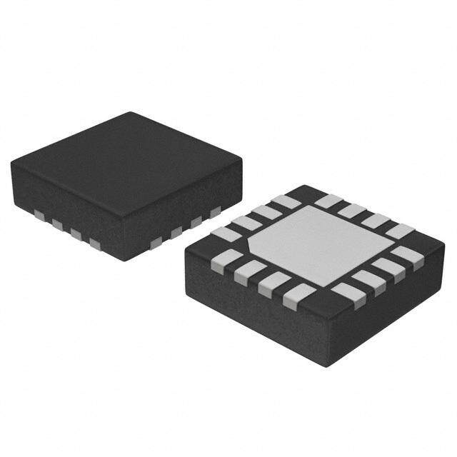
| 产品图片 |
|
| rohs | 符合RoHS无铅 / 符合限制有害物质指令(RoHS)规范要求 |
| 产品系列 | 时钟和计时器IC,时钟驱动器及分配,Analog Devices AD9508BCPZ- |
| 数据手册 | |
| 产品型号 | AD9508BCPZ |
| PCN组件/产地 | |
| PCN设计/规格 | |
| 乘法/除法因子 | 1:4 |
| 产品种类 | 时钟驱动器及分配 |
| 供应商器件封装 | 24-LFCSP-WQ(4x4) |
| 包装 | 托盘 |
| 商标 | Analog Devices |
| 安装类型 | 表面贴装 |
| 安装风格 | SMD/SMT |
| 封装 | Tray |
| 封装/外壳 | 24-WFQFN 裸露焊盘,CSP |
| 封装/箱体 | LFCSP-24 |
| 工作温度 | -40°C ~ 85°C |
| 工厂包装数量 | 490 |
| 差分-输入:输出 | 是/是 |
| 最大工作温度 | + 85 C |
| 最大输出频率 | 1650 MHz |
| 最小工作温度 | - 40 C |
| 标准包装 | 1 |
| 比率-输入:输出 | 1:4 |
| 电压-电源 | 2.375 V ~ 3.465 V |
| 电源电压-最大 | 3.465 V |
| 电源电压-最小 | 2.375 V |
| 电路数 | 1 |
| 类型 | 扇出缓冲器(分配),除法器 |
| 系列 | AD9508 |
| 输入 | CMOS |
| 输入类型 | Clock |
| 输出 | CMOS,HSTL,LVDS |
| 输出类型 | LVDS, HSTL, CMOS |
| 频率-最大值 | 1.65GHz |


- 商务部:美国ITC正式对集成电路等产品启动337调查
- 曝三星4nm工艺存在良率问题 高通将骁龙8 Gen1或转产台积电
- 太阳诱电将投资9.5亿元在常州建新厂生产MLCC 预计2023年完工
- 英特尔发布欧洲新工厂建设计划 深化IDM 2.0 战略
- 台积电先进制程称霸业界 有大客户加持明年业绩稳了
- 达到5530亿美元!SIA预计今年全球半导体销售额将创下新高
- 英特尔拟将自动驾驶子公司Mobileye上市 估值或超500亿美元
- 三星加码芯片和SET,合并消费电子和移动部门,撤换高东真等 CEO
- 三星电子宣布重大人事变动 还合并消费电子和移动部门
- 海关总署:前11个月进口集成电路产品价值2.52万亿元 增长14.8%


PDF Datasheet 数据手册内容提取
1.65 GHz Clock Fanout Buffer with Output Dividers and Delay Adjust Data Sheet AD9508 FEATURES FUNCTIONAL BLOCK DIAGRAM 1.65 GHz differential clock inputs/outputs 10-bit programmable dividers, 1 to 1024, all integers AD9508 OUT0 DIV/Φ Up to 4 differential outputs or 8 CMOS outputs OUT0 CLK Pin strapping capability for hardwired programming at OUT1 DIV/Φ power-up CLK OUT1 <115 fs rms broadband random jitter (see Figure 25) OUT2 DIV/Φ OUT2 Additive output jitter: 41 fs rms typical (12 kHz to 20 MHz) OUT3 Excellent output-to-output isolation SCLK/SCL/S0 DIV/Φ OUT3 Automatic synchronization of all outputs SDIO/SDA/S1 CONTROL INTERFACE Single 2.5 V/3.3 V power supply SDO/S3 SPI/I2C/PINS CS/S2 Internal LDO (low drop-out) voltage regulator for enhanced Phpaosew oefrf ssuetp spelyle icmt mfour noiutytp ut-to-output coarse delay adjust PIN CONTROL RESET SYNC 11161-001 3 programmable output logic levels, LVDS, HSTL, and CMOS Figure 1. Serial control port (SPI/I2C) or pin-programmable mode Space-saving 24-lead LFCSP APPLICATIONS Low jitter, low phase noise clock distribution Clocking high speed ADCs, DACs, DDSs, DDCs, DUCs, MxFEs High performance wireless transceivers High performance instrumentation Broadband infrastructure GENERAL DESCRIPTION The AD9508 provides clock fanout capability in a design that Each output has a programmable divider that can be bypassed emphasizes low jitter to maximize system performance. This or be set to divide by any integer up to 1024. In addition, the device benefits applications like clocking data converters with AD9508 supports a coarse output phase adjustment between demanding phase noise and low jitter requirements. the outputs. There are four independent differential clock outputs, each with The device can also be pin programmed for various fixed various types of logic levels available. Available logic types configurations at power-up without the need for SPI or I2C include LVDS (1.65 GHz), HSTL (1.65 GHz), and 1.8 V CMOS programming. (250 MHz). In 1.8 V CMOS output mode, the differential output The AD9508 is available in a 24-lead LFCSP and operates from becomes two CMOS single-ended signals. The CMOS outputs a either a single 2.5 V or 3.3 V supply. The temperature range is are 1.8 V logic levels, regardless of the operating supply voltage. −40°C to +85°C. Rev. G Document Feedback Information furnished by Analog Devices is believed to be accurate and reliable. However, no responsibility is assumed by Analog Devices for its use, nor for any infringements of patents or other One Technology Way, P.O. Box 9106, Norwood, MA 02062-9106, U.S.A. rights of third parties that may result from its use. Specifications subject to change without notice. No license is granted by implication or otherwise under any patent or patent rights of Analog Devices. Tel: 781.329.4700 ©2013–2017 Analog Devices, Inc. All rights reserved. Trademarks and registered trademarks are the property of their respective owners. Technical Support www.analog.com
AD9508 Data Sheet TABLE OF CONTENTS Features .............................................................................................. 1 Clock Input.................................................................................. 23 Applications ....................................................................................... 1 Clock Outputs ............................................................................. 24 Functional Block Diagram .............................................................. 1 Clock Dividers ............................................................................ 24 General Description ......................................................................... 1 Phase Delay Control .................................................................. 24 Revision History ............................................................................... 3 Reset Modes ................................................................................ 25 Specifications ..................................................................................... 4 Power-Down Mode .................................................................... 25 Electrical Characteristics ............................................................. 4 Output Clock Synchronization ................................................. 25 Power Supply Current and Temperature Conditions .............. 4 Power Supply ............................................................................... 25 Clock Inputs and Output DC Specifications ............................ 5 Thermally Enhanced Package Mounting Guidelines ............ 25 Output Driver Timing Characteristics ...................................... 6 Pin Strapping to Program on Power-Up ..................................... 26 Logic Inputs ................................................................................... 7 Serial Control Port ......................................................................... 27 Serial Port Specifications—SPI Mode ........................................ 7 SPI/I2C Port Selection ................................................................ 27 Serial Port Specifications—I2C Mode ........................................ 8 SPI Serial Port Operation .......................................................... 27 External Resistor Values For Pin Strapping Mode ................... 9 I2C Serial Port Operation .......................................................... 30 Clock Output Additive Phase Noise .......................................... 9 Register Map ................................................................................... 33 Clock Output Additive Time Jitter ........................................... 10 Register Map Bit Descriptions ...................................................... 34 Absolute Maximum Ratings .......................................................... 11 Serial Port Configuration (Register 0x00) .............................. 34 Thermal Characteristics ............................................................ 11 Silicon Revision (Register 0x0A to Register 0x0D) ............... 34 ESD Caution ................................................................................ 11 Chip Level Functions (Register 0x12 to Register 0x14) ........ 34 Pin Configuration and Function Descriptions ........................... 12 OUT0 Functions (Register 0x15 to Register 0x1A) ............... 35 Typical Performance Characteristics ........................................... 14 OUT1 Functions (Register 0x1B to Register 0x20) ............... 36 Test Circuits ..................................................................................... 20 OUT2 Functions (Register 0x21 to Register 0x26) ................ 37 Input/Output Termination Recommendations ...................... 20 OUT3 Functions (Register 0x27 to Register 0x2C) ............... 38 Terminology .................................................................................... 21 Packaging and Ordering Information ......................................... 40 Theory of Operation ...................................................................... 22 Outline Dimensions ................................................................... 40 Detailed Block Diagram ............................................................ 22 Ordering Guide .......................................................................... 40 Programming Mode Selection .................................................. 22 Rev. G | Page 2 of 40
Data Sheet AD9508 REVISION HISTORY 6/2017—Rev. F to Rev. G 2/2014—Rev. B to Rev. C Updated Outline Dimensions ........................................................ 40 Changes to Table 14 ........................................................................ 22 Changes to Ordering Guide ........................................................... 40 10/2013—Rev. A to Rev. B 4/2015—Rev. E to Rev. F Change to Figure 5 Caption ........................................................... 13 Changes to Clock Outputs Section ............................................... 24 Change to Figure 13 Caption ......................................................... 14 Changes to Table 28 ........................................................................ 35 Change to Figure 19 Caption ......................................................... 15 Changes to Table 30 ........................................................................ 36 Change to Individual Clock Channel Power-Down Section .... 23 Changes to Table 32 ........................................................................ 38 Change to Write Section ................................................................ 27 Changes to Table 34 ........................................................................ 39 Changes to Table 27 ........................................................................ 34 Changes to Table 29 ........................................................................ 35 11/2014—Rev. D to Rev. E Changes to Table 31 ........................................................................ 36 Changes to Figure 1 .......................................................................... 1 Changes to Table 33 ........................................................................ 37 Moved Revision History Section ..................................................... 3 Changes to Table 12 ........................................................................ 12 4/2013—Rev. 0 to Rev. A Changes to Clock Outputs Section, Clock Dividers Section, and Changes to Table 9 ............................................................................ 9 Phase Delay Control Section ......................................................... 24 Changes to Figure 10 ...................................................................... 14 Changed Individual Clock Channel Power-Down Section to Changes to Figure 15 ...................................................................... 15 Individual Clock Divider Power-Down Section ......................... 25 Changes to Figure 24 and Figure 26 ............................................. 16 Changes to Individual Clock Divider Power-Down Section and Changes to Figure 27, Figure 29 to Figure 32.............................. 17 Output Clock Synchronization Section ........................................ 25 Changes to Figure 33 ...................................................................... 18 Changes to Pin Strapping to Program on Power-up Section and Table 15 ............................................................................................. 26 1/2013—Revision 0: Initial Version Changes to Table 27 and Table 28 ................................................. 35 Changes to Table 29 and Table 30 ................................................. 36 Changes to Table 31 and Table 32 ................................................. 37 Changes to Table 33 ........................................................................ 38 Changes to Table 34 ........................................................................ 39 9/2014—Rev. C to Rev. D Changes to Table 1 ............................................................................ 3 Changes to Table 2 ............................................................................ 4 Changes to Figure 37 Caption; Added Figure 38; Renumbered Sequentially ...................................................................................... 19 Changes to Clock Input Section and Table 14 ............................. 23 Rev. G | Page 3 of 40
AD9508 Data Sheet SPECIFICATIONS ELECTRICAL CHARACTERISTICS Typical values are given for V = 3.3 V and 2.5 V and T = 25°C; minimum and maximum values are given over the full V = 3.3 V + 5% down S A DD to 2.5 V − 5% and T = −40°C to +85°C variation; and input slew rate > 1 V/ns, unless otherwise noted. A POWER SUPPLY CURRENT AND TEMPERATURE CONDITIONS Table 1. Parameter Min Typ Max Unit Test Conditions/Comments SUPPLY VOLTAGE 2.375 2.5 3.465 V Use supply voltage setting (2.5 V or 3.3 V) and appropriate current consumption configuration (see Current Consumption parameters in Table 1) to calculate total power dissipation CURRENT CONSUMPTION LVDS Configuration 165 182 mA Input clock: 1500 MHz in differential mode, all LVDS output drivers at 1500 MHz 122 134 mA Input clock: 800 MHz in differential mode, all LVDS output drivers at 200 MHz HSTL Configuration 194 213 mA Input clock: 1500 MHz in differential mode, all HSTL output drivers at 1500 MHz 131 144 mA Input clock: 491.52 MHz in differential mode, all output drivers at 491.52 MHz 92 101 mA Input clock: 122.88 MHz in differential mode, all output drivers at 122.88 MHz CMOS Configuration 141 185 mA Input clock: 1500 MHz in differential mode, all CMOS output drivers at 250 MHz, 10 pF load 122 134 mA Input clock: 800 MHz in differential mode, all CMOS outputs drivers at 200 MHz, 10 pF load 85 94 mA Input clock: 100 MHz in differential mode, all CMOS outputs drivers at 100 MHz, 10 pF load Full Power-Down 6 10 mA TEMPERATURE Ambient Temperature Range, TA −40 +25 +85 °C Junction Temperature, T 115 °C Junction temperatures above 115°C can J degrade performance but no damage should occur, unless the absolute temperature is exceeded Rev. G | Page 4 of 40
Data Sheet AD9508 CLOCK INPUTS AND OUTPUT DC SPECIFICATIONS Table 2. Parameter Symbol Min Typ Max Unit Test Conditions/Comments CLOCK INPUTS Differential Mode Input Frequency 0 1650 MHz Differential input Input Sensitivity 360 2200 mV p-p As measured with a differential probe; jitter performance improves with higher slew rates (greater voltage swing) Input Common-Mode Voltage V 0.95 1.05 1.15 V Input pins are internally self biased, which ICM enables ac coupling Input Voltage Offset 30 mV DC-Coupled Input Common- V 0.58 1.67 V This is the allowable common-mode CMR Mode Range voltage range when dc-coupled Pulse Width Low 303 ps High 303 ps Input Resistance (Single-Ended) 5.0 7 9 kΩ Input Capacitance C 2 pF IN Input Bias Current (Each Pin) 100 400 µA Full input swing CMOS CLOCK MODE (SINGLE-ENDED) 2.5 V or 3.3 V CMOS only; for 1.8 V CMOS, use (ac-coupled) differential input mode Input Frequency 250 MHz Input Voltage High V VDD/2 + 0.15 V IH Low V VDD/2 − 0.15 V IL Input Current High I 1 µA INH Low IINL −142 µA Input Capacitance C 2 pF IN LVDS CLOCK OUTPUTS Termination = 100 Ω differential (OUTx, OUTx) Output Frequency 1650 MHz Output Voltage Differential V 247 375 454 mV V − V measurement across a differential OD OH OL pair at the default amplitude setting with output driver not toggling; see Figure 6 for variation over frequency Delta V ΔV 50 mV This is the absolute value of the difference OD OD between V when the normal output is high OD vs. when the complementary output is high Offset Voltage V 1.125 1.18 1.375 V (V + V )/2 across a differential pair OS OH OL Delta V ΔV 50 mV This is the absolute value of the difference OS OS between V when the normal output is high OS vs. when the complementary output is high Short-Circuit Current IA, IB 13.6 24 mA Each pin (output shorted to GND) S S LVDS Duty Cycle 45 55 % Up to 750 MHz input 39 61 % 750 MHz to1500 MHz input 50.1 % 1650 MHz input HSTL CLOCK OUTPUTS 100 Ω across differential pair; default amplitude setting Output Frequency 1650 MHz Differential Output Voltage V 859 925 978 mV V − V with output driver static O OH OL Common-Mode Output Voltage V 905 940 971 mV (V + V )/2 with output driver static OCM OH OL HSTL Duty Cycle 45 55 % Up to 750 MHz input 40 60 % 750 MHz to 1500 MHz input 50.9 % 1650 MHz input Rev. G | Page 5 of 40
AD9508 Data Sheet Parameter Symbol Min Typ Max Unit Test Conditions/Comments CMOS CLOCK OUTPUTS Single-ended; termination = open; OUTx and OUTx in phase Output Frequency 250 MHz With 10 pF load per output, see Figure 14 for swing vs. frequency Output Voltage At 1 mA Load High V 1.7 V OH Low V 0.1 V OL At 10 mA load High V 1.2 V OH Low V 0.6 V OL At 10 mA Load (2 × CMOS Mode) High V 1.45 V OH Low V 0.35 V OL CMOS Duty Cycle 45 55 % Up to 250 MHz OUTPUT DRIVER TIMING CHARACTERISTICS Table 3. Parameter Symbol Min Typ Max Unit Test Conditions/Comments LVDS OUTPUTS Termination = 100 Ω differential, 1 × LVDS Output Rise/Fall Time t , t 152 177 ps 20% to 80% measured differentially R F Propagation Delay, Clock-to-LVDS Output t 1.56 2.01 2.43 ns PD Temperature Coefficient 2.8 ps/°C Output Skew1 All LVDS Outputs On the Same Part 48 ps Across Multiple Parts 781 ps Assumes same temperature and supply; takes into account worst-case propagation delay delta due to worst-case process variation HSTL OUTPUTS Termination = 100 Ω differential, 1 × HSTL Output Rise/Fall Time t , t 118 143 ps 20% to 80% measured differentially R F Propagation Delay, Clock-to-HSTL Output t 1.59 2.05 2.5 ns PD Temperature Coefficient 2.9 ps/°C Output Skew1 All HSTL Outputs On the Same Part 59 ps Across Multiple Parts 825 ps Assumes same temperature and supply; takes into account worst-case propagation delay delta due to worst-case process variation CMOS OUTPUTS Output Rise/Fall Time t t 1.18 1.45 ns 20% to 80%; C = 10 pF R, F LOAD Propagation Delay, Clock-to-CMOS Output t 2.04 2.56 3.07 ns 10 pF load PD Temperature Coefficient 3.3 ps/°C Output Skew1 All CMOS Outputs On the Same Part 112 ps Across Multiple Parts 965 ps Assumes same temperature and supply; takes into account worst-case propagation delay delta due to worst-case process variation Rev. G | Page 6 of 40
Data Sheet AD9508 Parameter Symbol Min Typ Max Unit Test Conditions/Comments OUTPUT LOGIC SKEW1 CMOS load = 10 pF and LVDS load = 100 Ω LVDS Output(s) and HSTL Output(s) 77 119 ps Outputs on the same device; assumes worst-case output combination LVDS Output(s) and CMOS Output(s) 497 700 ps Outputs on the same device; assumes worst-case output combination HSTL Output(s) and CMOS Output(s) 424 622 ps Outputs on the same device; assumes worst-case output combination 1 Output skew is the difference between any two similar delay paths while operating at the same voltage and temperature. LOGIC INPUTS Table 4. Parameter Symbol Min Typ Max Unit Test Conditions/Comments LOGIC INPUTS RESET, SYNC, IN_SEL Input Voltage High V 1.7 V 2.5 V supply voltage operation IH 2.0 V 3.3 V supply voltage operation Low V 0.7 V 2.5 V supply voltage operation IL 0.8 V 3.3 V supply voltage operation Input Current I , I −300 +100 µA INH INL Input Capacitance C 2 pF IN SERIAL PORT SPECIFICATIONS—SPI MODE Table 5. Parameter Min Typ Max Unit Test Conditions/Comments CS SCLK has a 200 kΩ internal pull-down resistor Input Voltage Logic 1 VDD − 0.4 V Logic 0 0.4 V Input Current Logic 1 −4 µA Logic 0 −85 µA Input Capacitance 2 µA SCLK Input Voltage Logic 1 VDD − 0.4 V Logic 0 0.4 V Input Current Logic 1 70 µA Logic 0 13 µA Input Capacitance 2 pF SDIO As Input Input Voltage Logic 1 VDD − 0.4 V Logic 0 0.4 V Input Current Logic 1 −1 µA Logic 0 −1 µA Input Capacitance 2 pF Rev. G | Page 7 of 40
AD9508 Data Sheet Parameter Min Typ Max Unit Test Conditions/Comments As Output Output Voltage Logic 1 VDD − 0.4 V 1 mA load current Logic 0 0.4 V 1 mA load current SDO Output Voltage Logic 1 VDD − 0.4 V 1 mA load current Logic 0 0.4 V 1 mA load current TIMING SCLK Clock Rate, 1/t 30 MHz CLK Pulse Width High, t 4.6 ns HIGH Pulse Width Low, t 3.5 ns LOW SDIO to SCLK Setup, t 2.9 ns DS SCLK to SDIO Hold, t 0 ns DH SCLK to Valid SDIO and SDO, t 15 ns DV CS to SCLK Setup (tS) 3.4 ns CS to SCLK Hold (tC) 0 ns CS to Minimum Pulse Width High 3.4 ns SERIAL PORT SPECIFICATIONS—I2C MODE Table 6. Parameter Min Typ Max Unit Test Conditions/Comments SDA, SCL (AS INPUT) Input Voltage Logic 1 VDD − 0.4 V Logic 0 0.4 V Input Current −40 0 µA For V = 10% to 90% DVDD3 IN Hysteresis of Schmitt Trigger Inputs 150 mV SDA (AS OUTPUT) Output Logic 0 Voltage 0.4 V I = 3 mA O Output Fall Time from V to V 250 ns 10 pF ≤ C ≤ 400 pF IH (MIN) IL (MAX) b TIMING SCL Clock Rate 400 kHz Bus-Free Time Between a Stop and Start 1.3 µs Condition, t BUF Repeated Start Condition Setup Time, t 0.6 µs SU; STA Repeated Hold Time Start Condition, t 0.6 µs After this period, the first clock pulse is HD; STA generated Stop Condition Setup Time, t 0.6 µs SU; STO Low Period of the SCL Clock, t 1.3 µs LOW High Period of the SCL Clock, t 0.6 µs HIGH Data Setup Time, t 100 ns SU; DAT Data Hold Time, t 0 0.9 µs HD; DAT Rev. G | Page 8 of 40
Data Sheet AD9508 EXTERNAL RESISTOR VALUES FOR PIN STRAPPING MODE Table 7. Parameter Resistor Polarity Min Typ Max Unit Test Conditions/Comments EXTERNAL RESISTORS Using 10% tolerance resistor Voltage Level 0 Pull down to ground 820 Ω Voltage Level 1 Pull down to ground 1.8 kΩ Voltage Level 2 Pull down to ground 3.9 kΩ Voltage Level 3 Pull down to ground 8.2 kΩ Voltage Level 4 Pull up to VDD 820 Ω Voltage Level 5 Pull up to VDD 1.8 kΩ Voltage Level 6 Pull up to VDD 3.9 kΩ Voltage Level 7 Pull up to VDD 8.2 kΩ CLOCK OUTPUT ADDITIVE PHASE NOISE Table 8. Parameter Min Typ Max Unit Test Conditions/Comments CLK-TO-HSTL OR LVDS ADDITIVE PHASE NOISE CLK = 1474.56 MHz, OUTx = 1474.56 MHz Input slew rate > 1 V/ns Divide Ratio = 1 At 10 Hz Offset −88 dBc/Hz At 100 Hz Offset −100 dBc/Hz At 1 kHz Offset −109 dBc/Hz At 10 kHz Offset −116 dBc/Hz At 100 kHz Offset −135 dBc/Hz At 1 MHz Offset −144 dBc/Hz At 10 MHz Offset −148 dBc/Hz At 100 MHz Offset −149 dBc/Hz CLK-TO-HSTL OR LVDS or CMOS ADDITIVE PHASE NOISE CLK = 625 MHz, OUTx = 125 MHz Input slew rate > 1 V/ns Divide Ratio = 5 At 10 Hz Offset −114 dBc/Hz At 100 Hz Offset −125 dBc/Hz At 1 kHz Offset −133 dBc/Hz At 10 kHz Offset −141 dBc/Hz At 100 kHz Offset −159 dBc/Hz At 1 MHz Offset −162 dBc/Hz At 10 MHz Offset −163 dBc/Hz At 20 MHz Offset −163 dBc/Hz CLK-TO-HSTL OR LVDS ADDITIVE PHASE NOISE CLK = 491.52 MHz, OUTx = 491.52 MHz Input slew rate > 1 V/ns Divide Ratio = 1 At 10 Hz Offset −100 dBc/Hz At 100 Hz Offset −111 dBc/Hz At 1 kHz Offset −120 dBc/Hz At 10 kHz Offset −127 dBc/Hz At 100 kHz Offset −146 dBc/Hz At 1 MHz Offset −153 dBc/Hz At 10 MHz Offset −153 dBc/Hz At 20 MHz Offset −153 dBc/Hz Rev. G | Page 9 of 40
AD9508 Data Sheet CLOCK OUTPUT ADDITIVE TIME JITTER Table 9. Parameter Min Typ Max Unit Test Conditions/Comments LVDS OUTPUT ADDITIVE TIME JITTER CLK = 622.08 MHz, Outputs = 622.08 MHz 41 fs rms BW = 12 kHz to 20 MHz 70 fs rms BW = 20 kHz to 80 MHz 69 fs rms BW = 50 kHz to 80 MHz CLK = 622.08 MHz, Outputs = 155.52 MHz 93 fs rms BW = 12 kHz to 20 MHz 144 fs rms BW = 20 kHz to 80 MHz 142 fs rms BW = 50 kHz to 80 MHz CLK = 125 MHz, Outputs = 125 MHz 105 fs rms BW = 12 kHz to 20 MHz 209 fs rms BW = 20 kHz to 80 MHz 206 fs rms BW = 50 kHz to 80 MHz CLK = 400 MHz, Outputs = 50 MHz 184 fs rms BW = 12 kHz to 20 MHz HSTL OUTPUT ADDITIVE TIME JITTER CLK = 622.08 MHz, Outputs = 622.08 MHz 41 fs rms BW = 12 kHz to 20 MHz 56 fs rms BW = 100 Hz to 20 MHz 72 fs rms BW = 20 kHz to 80 MHz 70 fs rms BW = 50 kHz to 80 MHz CLK = 622.08 MHz, Outputs = 155.52 MHz 76 fs rms BW = 12 kHz to 20 MHz 87 fs rms BW = 100 Hz to 20 MHz 158 fs rms BW = 20 kHz to 80 MHz 156 fs rms BW = 50 kHz to 80 MHz CMOS OUTPUT ADDITIVE TIME JITTER CLK = 100 MHz, Outputs = 100 MHz 91 fs rms BW = 12 kHz to 20 MHz Rev. G | Page 10 of 40
Data Sheet AD9508 ABSOLUTE MAXIMUM RATINGS Values of θ are provided for package comparison and PCB Table 10. JC design considerations when an external heat sink is required. Parameter Rating Supply Voltage (VDD) 3.6 V Values of θJB are provided for package comparison and PCB Maximum Digital Input Voltage −0.5 V to VDD + 0.5 V design considerations. CLK and CLK −0.5 V to VDD + 0.5 V THERMAL CHARACTERISTICS Maximum Digital Output Voltage −0.5 V to VDD + 0.5 V Thermal characteristics established using JEDEC51-7 and Storage Temperature Range −65°C to +150°C JEDEC51-5 2S2P test boards. Operating Temperature Range −40°C to +85°C Lead Temperature (Soldering 10 sec) 300°C Table 11. Thermal Characteristics, 24-Lead LFCSP Junction Temperature 150°C Thermal Characteristic (JEDEC51-7 and JEDEC51-5 2S2P Stresses at or above those listed under Absolute Maximum Symbol Test Boards1) Value2 Unit Ratings may cause permanent damage to the product. This is a θ Junction-to-ambient thermal 43.5 °C/W JA stress rating only; functional operation of the product at these resistance per JEDEC JESD51-2 (still air) or any other conditions above those indicated in the operational θ Junction-to-ambient thermal 40 °C/W section of this specification is not implied. Operation beyond JMA resistance, 1.0 m/sec airflow per the maximum operating conditions for extended periods may JEDEC JESD51-6 (moving air) affect product reliability. θ Junction-to-ambient thermal 38.5 °C/W JMA The following equation determines the junction temperature on resistance, 2.5 m/sec airflow per JEDEC JESD51-6 (moving air) the application PCB: θ Junction-to-board thermal 16.2 °C/W JB TJ = TCASE + (ΨJT × PD) resistance per JEDEC JESD51-8 (still air) where: θ Junction-to-case thermal resistance 7.1 °C/W T is the junction temperature (°C). JC J (die-to-heat sink) per MIL-STD-883, T is the case temperature (°C) measured by the customer at CASE Method 1012.1 the top center of the package. Ψ Junction-to-top-of-package 0.33 °C/W JT ΨJT is the value as indicated in Table 11. characterization parameter per PD is the power dissipation. JEDEC JESD51-2 (still air) Values of θ are provided for package comparison and PCB 1 The exposed pad on the bottom of the package must be soldered to ground JA (VSS) to achieve the specified thermal performance. design considerations. θJA can be used for a first-order approxi- 2 Results are from simulations. The PCB is a JEDEC multilayer type. Thermal mation of T by the following equation: performance for actual applications requires careful inspection of the J conditions in the application to determine if they are similar to those TJ = TA + (θJA × PD) assumed in these calculations. where T is the ambient temperature (°C). A ESD CAUTION Rev. G | Page 11 of 40
AD9508 Data Sheet PIN CONFIGURATION AND FUNCTION DESCRIPTIONS 1S 0S A/DS/OIDS LES_NI KLC KLC CNYS /LCS/KLCS 42 32 22 12 02 91 CS/S21 18RESET OUT02 17OUT3 OUT03 AD9508 16OUT3 SDO/S34 TOP VIEW 15PROG_SEL EXT_CAP05 14EXT_CAP1 VDD6 13VDD 7 8 9 01 11 21 1 1 4 5 2 2 T T S S T T U U U U O O O O NOTES 11161-002 1.THE EXPOSED DIE PAD MUST BE CONNECTED TO GROUND(VSS). Figure 2. Pin Configuration Table 12. Pin Function Descriptions Pin No. Mnemonic Description 1 CS/S2 Chip Select/Pin Programming. Multipurpose pin. This pin is controlled by the PROG_SEL pin. Chip Select (CS) is an active logic low CMOS input used in the SPI operation mode. When programming a device via SPI mode, CS must be held low. In systems where more than one AD9508 is present, this pin enables individual programming of each AD9508. In pin programming mode, this pin becomes S2. In this mode, S2 is hard wired with a resistor to either VDD or ground. The resistor value and resistor biasing determine the output divider value for the outputs on Pin 11 and Pin 12. See the Pin Strapping to Program on Power-Up section for more details. 2 OUT0 LVDS/HSTL Differential Output or Single-Ended CMOS Output. 3 OUT0 Complementary LVDS/HSTL Differential Output or Single-Ended CMOS Output. 4 SDO/S3 Serial Data Output/Pin Programming. Multipurpose pin. This pin is controlled by the PROG_SEL pin. SDO is configured as an output to read back the internal register settings in SPI mode operation. In pin programming mode, this pin becomes S3, which is hard wired with a resistor to either VDD or ground. The resistor value and resistor biasing determine the output divider value for the outputs on Pin 16 and Pin 17. See the Pin Strapping to Program on Power-Up section for more details. 5 EXT_CAP0 Node for External Decoupling Capacitor for LDO. Tie this pin to a 0.47 µF capacitor to ground. 6 VDD Power Supply (2.5 V or 3.3 V Operation). 7 OUT1 LVDS/HSTL Differential Output or Single-Ended CMOS Output. 8 OUT1 Complementary LVDS/HSTL Differential Output or Single-Ended CMOS Output. 9 S4 Pin Programming. Use this pin in pin programming mode only. The PROG_SEL pin determines which programming mode is used. In pin programming mode, S4 is hardwired with a resistor to either VDD or ground. The resistor value and resistor biasing determine the output logic levels used for the outputs on Pin 2, Pin 3, Pin 7, and Pin 8. See the Pin Strapping to Program on Power-Up section for more details. 10 S5 Pin Programming. Use this pin in pin programming mode only. The PROG_SEL pin determines which programming mode is used. In pin programming mode, S5 is hardwired with a resistor to either VDD or ground. The resistor value and resistor biasing determine the output logic levels used for the outputs on Pin 11, Pin 12, Pin 16, and Pin 17. See the Pin Strapping to Program on Power-Up section for more details. 11 OUT2 LVDS/HSTL Differential Output or Single-Ended CMOS Output. 12 OUT2 Complementary LVDS/HSTL Differential Output or Single-Ended CMOS Output. 13 VDD Power Supply (2.5 V or 3.3 V Operation). 14 EXT_CAP1 Node for External Decoupling Capacitor for LDO. Tie this pin to a 0.47 µF capacitor to ground. 15 PROG_SEL Three-State CMOS Input. Pin 15 selects the type of device programming interface to be used (SPI, I2C, or pin programming). 16 OUT3 LVDS/HSTL Differential Output or Single-Ended CMOS Output. 17 OUT3 Complementary LVDS/HSTL Differential Output or Single-Ended CMOS Output. Rev. G | Page 12 of 40
Data Sheet AD9508 Pin No. Mnemonic Description 18 RESET CMOS Input. Device Reset. When this active low pin is asserted, the internal register settings enter their default state after the RESET is released. Note that RESET also serves as a power-down of the device while an active low signal is applied to the pin. The RESET pin has an internal 24 kΩ pull-up resistor. 19 SCLK/SCL/S0 Serial Programming Clock/Data Clock/Programming Pin. Multipurpose pin controlled by the PROG_SEL pin used for serial programming clock (SCLK) in SPI mode or data clock (SCL) for serial programming in I2C Mode. The PROG_SEL pin determines which programming mode is used. In pin programming mode, this pin becomes S0. In this mode, S0 is hardwired with a resistor to either VDD or ground. The resistor value and resistor biasing determine the output divider values for the outputs on Pin 2 and Pin 3. See the Pin Strapping to Program on Power-Up section for more details. 20 SYNC Clock Synchronization. When this pin is active low, the output drivers are held static and then synchronized on a low-to-high transition of this pin. The SYNC pin has an internal 24 kΩ pull-up resistor. 21 CLK Differential Clock Input or Single-Ended CMOS Input. Whether this pin serves as the differential clock input or the single-ended CMOS input depends on the logic state of the IN_SEL pin. 22 CLK Complementary Differential Clock Input. 23 IN_SEL CMOS Input. A logic high configures the CLK and CLK inputs for a differential input signal. A logic low configures the input for single-ended CMOS applied to the CLK pin. AC-couple the unused CLK to ground with a 0.1 µF capacitor. 24 SDIO/SDA/S1 Serial Data Input and Output (SPI)/Serial Data (I2C)/Pin Programming. Pin 24 is a multipurpose input controlled by the PROG_SEL pin used for SPI (SDIO), I2C (SDA), and pin strapping modes (S1). When the device is in 4-wire SPI mode, data is written via SDIO. In 3-wire mode, both data reads and writes occur on this pin. There is no internal pull-up/pull-down resistor on this pin. In I2C mode, SDA serves as the serial data pin. The PROG_SEL pin determines which programming mode is used. In pin programming mode, this pin becomes S1. In this mode, S1 is hardwired with a resistor to either VDD or ground. The resistor value and resistor biasing determine the output divider values for the outputs on Pin 7 and Pin 8. See the Pin Strapping to Program on Power-Up section for more details. EP Exposed Pad. The exposed die pad must be connected to ground (VSS). Rev. G | Page 13 of 40
AD9508 Data Sheet TYPICAL PERFORMANCE CHARACTERISTICS 800 p) p- V m G ( 700 DIV) WIN mV/ T S E (100 UTPU 600 VOLTAG TIAL O N E 500 R E F F DI TIME (250ps/DIV) 11161-003 400100 300 500 FRE7Q00UENCY9 0(M0Hz) 1100 1300 1500 11161-006 Figure 3. LVDS Differential Output Waveform at 800 MHz Figure 6. LVDS Differential Output Swing vs. Frequency 800 p) p- V 780 m V) G ( V/DI WIN m S 760 TAGE (100 L OUTPUT 740 L A VO NTI E R E 720 F F DI TIME (1.5ns/DIV) 11161-004 7002.3 2.5 2.7POWER S2.U9PPLY (V3).1 3.3 3.5 11161-008 Figure 4. LVDS Differential Output Waveform at 156.25 MHz Figure 7. LVDS Differential Output Swing vs. Power Supply Voltage 200 2.4 ONE OUTPUT (mA) TWO OUTPUTS (mA) THREE OUTPUTS (mA) 2.3 FOUR OUTPUTS (mA) 150 s) n 2.2 Y ( A) LA RRENT (m 100 ATION DE 22..01 U G C A P 50 PRO 1.9 1.8 0 1.7 0 400 FREQUE8N0C0Y (MHz) 1200 1600 11161-005 0.2 0.4 0.6 INP0U.8T DIF1F.0EREN1T.2IAL (V1. 4p-p) 1.6 1.8 2.0 11161-009 Figure 5. Power Supply Current vs. Input Frequency and Number of Outputs Figure 8. LVDS Propagation Delay vs. Input Differential Voltage Used, LVDS Rev. G | Page 14 of 40
Data Sheet AD9508 2.6 2.4 s) n LAY ( 2.2 DIV) ON DE 2.0 00mV/ ATI E (3 G G PA 1.8 TA O L R O P V 1.6 1.4300 500 COM7M00ON-MOD9E0 0VOLTAG11E0 (0mV) 1300 1500 11161-010 TIME (5ns/DIV) 11161-013 Figure 9. LVDS Propagation Delay vs. Input Common-Mode Voltage Figure 12. CMOS Output Waveform at 50 MHz with 10 pF Load 60 DIVIDER 1 125 DIVIDER 2 (FREQUENCY RANGE NORMALIZED FROM 0Hz TO 800MHz) ONE OUTPUT (mA) DIVIDER 3 (FREQUENCY RANGE NORMALIZED FROM 0Hz TO 500MHz) TWO OUTPUTS (mA) THREE OUTPUTS (mA) FOUR OUTPUTS (mA) 55 FIVE OUTPUTS (mA) 100 SIX OUTPUTS (mA) SEVEN OUTPUTS (mA) %) EIGHT OUTPUTS (mA) LE ( mA) CYC 50 NT ( 75 Y RE DUT CUR 45 50 40 0 200 400 6F0R0EQUE8N00CY (M1H00z0) 1200 1400 1600 11161-011 2525 50 75 100FREQ12U5ENC1Y5 (0MHz1)75 200 225 250 11161-014 Figure 10. LVDS Output Duty Cycle vs. Output Frequency Figure 13. Power Supply Current vs. Input Frequency vs. Number of Outputs Used, CMOS 1.9 300ΩLOAD 500ΩLOAD 750ΩLOAD 1kΩLOAD 1.8 p) V) p- DI V mV/ NG ( 1.7 00 WI GE (3 UT S 1.6 A P T T L U O O V 1.5 TIME (1.25ns/DIV) 11161-012 1.40 50 FR1E00QUENCY (1M5H0z) 200 250 11161-015 Figure 11. CMOS Output Waveform at 200 MHz with 10 pF Load Figure 14. CMOS Output Swing vs. Frequency and Resistive Load Rev. G | Page 15 of 40
AD9508 Data Sheet 2.0 1.8 p) p- G (V 1.6 DIV) N V/ WI m UTPUT S 1.4 AGE (300 O LT O 1.2 V –40°C +25°C +85°C 1.00 50 FR1E00QUENCY (1M5H0z) 200 250 11161-016 TIME (1.5ns/DIV) 11161-019 Figure 15. CMOS Output Swing vs. Frequency and Temperature (10 pF Load) Figure 18. HSTL Differential Output Waveform at 156.25 MHz 1.9 200 ONE OUTPUT (mA) TWO OUTPUTS (mA) THREE OUTPUTS (mA) FOUR OUTPUTS (mA) 1.7 150 p) V p- A) NG ( T (m WI 1.5 EN 100 S R UT UR P C T U O 1.3 50 2pF LOAD 5pF LOAD 10pF LOAD 20pF LOAD 1.10 50 FR1E00QUENCY (M15H0z) 200 250 11161-017 00 400 FREQUE8N0C0Y (MHz) 1200 1600 11161-020 Figure 16. CMOS Output Swing vs. Frequency and Capacitive Load Figure 19. Power Supply Current vs. Input Frequency and Number of Outputs (2 pF, 5 pF, 10 pF, 20 pF) Used, HSTL 2.0 p-p) 1.9 V m G ( 1.8 DIV) WIN 1.7 mV/ T S 00 PU 1.6 3 T LTAGE ( TIAL OU 1.5 O N V E 1.4 R E F DIF 1.3 TIME (250ps/DIV) 11161-018 1.2100 300 500 FRE7Q00UENCY9 0(M0Hz) 1100 1300 1500 11161-007 Figure 17. HSTL Differential Output Waveform at 800 MHz Figure 20. HSTL Differential Output Swing vs. Frequency Rev. G | Page 16 of 40
Data Sheet AD9508 2.0 60 DIVIDER 1 DIVIDER 2 (FREQUENCY RANGE NORMALIZED FROM 0Hz TO 800MHz) p) DIVIDER 3 (FREQUENCY RANGE NORMALIZED FROM 0Hz TO 500MHz) p- V 1.9 m G ( 55 N WI %) T S 1.8 LE ( U C P Y 50 T C L OU 1.7 UTY A D TI N E 45 R E 1.6 F F DI 1.5 40 2.3 2.5 2.7POWER S2.U9PPLY (V3).1 3.3 3.5 11161-021 0 200 400 6F0R0EQUE8N00CY (M1H00z0) 1200 1400 1600 11161-024 Figure 21. HSTL Differential Output Swing vs. Power Supply Voltage Figure 24. HSTL Output Duty Cycle vs. Output Frequency 2.4 150 2.3 140 ns) 2.2 130 Y ( ON DELA 2.1 R (fsrms) 120 ATI 2.0 TE 110 G T A JI P RO 1.9 100 P 1.8 90 1.7 80 0.2 0.4 0.6 INP0U.8T DIF1F.0EREN1T.2IAL (V1. 4p-p) 1.6 1.8 2.0 11161-022 0 2 SL4EW RATE (V/6ns) 8 10 11161-227 Figure 22. HSTL Propagation Delay vs. Input Differential Voltage Figure 25. Additive Broadband Jitter vs. Input Slew Rate, LVDS, HSTL (Calculated from SNR of ADC Method) 2.6 –80 HSTL 155.52MHz HSTL 311.04MHz –90 HSTL 622.08MHz 2.4 –100 LAY (ns) 2.2 Bc/Hz)–110 E d ROPAGATION D 21..08 PHASE NOISE (–––111432000 P –150 1.6 –160 1.4 –170 300 500 COM7M00ON-MOD9E0 0VOLTAG11E0 (0mV) 1300 1500 11161-023 10 100 1kFREQU1E0NkCY OF10F0SkET (Hz1)M 10M 100M 11161-228 Figure 23. HSTL Propagation Delay vs. Input Common-Mode Voltage Figure 26. Absolute Phase Noise in HSTL Mode with Clock Input at 622.08 MHz and Outputs = 622.08 MHz, 311.04 MHz, 155.52 MHz Rev. G | Page 17 of 40
AD9508 Data Sheet –80 –80 LVDS 155.52MHz MARKER LVDS 311.04MHz FREQUENCY AMPLITUDE –90 LVDS 622.08MHz –90 1. 10Hz –116.04dBc/Hz 2. 100Hz –126.68dBc/Hz –100 3. 1kHz –135.27dBc/Hz Hz)–100 Hz) 45.. 1100k0H.5zkHz ––114529..5462ddBBcc//HHzz Bc/–110 Bc/–110 1 67.. 11M0MHHzz ––116614..9575ddBBcc//HHzz d d E ( E (–120 2 OIS–120 OIS E N E N–130 3 S–130 S HA HA–140 4 P P –140 –150 5 6 –150 –160 7 –16010 100 1kFREQU1E0NkCY OF10F0SkET (Hz1)M 10M 100M 11161-229 –17010 100 1k FR1E0QkUENC1Y0 0(Hkz) 1M 10M 100M 11161-330 Figure 27. Absolute Phase Noise in LVDS Mode with Clock Input at Figure 30. Additive Phase Noise with Clock Input = 1500 MHz with HSTL 622.08 MHz and Outputs = 622.08 MHz, 311.04 MHz, 155.52 MHz Outputs = 100 MHz –80 –80 MARKER FREQUENCY AMPLITUDE –90 –90 1. 10Hz –112.35dBc/Hz 2. 100Hz –118.81dBc/Hz –100 –100 3. 1kHz –127.84dBc/Hz Hz) Hz) 1 45.. 1100k0H.5zkHz ––113551..9971ddBBcc//HHzz c/–110 c/–110 6. 1MHz –157.87dBc/Hz E (dB–120 E (dB–120 2 78.. 1200MMHHzz ––115597..7888ddBBcc//HHzz S S 3 OI OI E N–130 E N–130 4 S S HA–140 HA–140 P P –150 –150 5 6 7 8 –160 –160 –1701 10F0R0EQUENCY O1F0F0S0E0T0 (MHz) 10000000 11161-230 –17010 100 1k FR1E0QkUENC1Y0 0(Hkz) 1M 10M 100M 11161-129 Figure 28. Absolute Phase Noise of Clock Source at 622.08 MHz Figure 31. Additive Phase Noise with Clock Input = 622.08 MHz with HSTL Outputs = 155.52 MHz –80 –80 1 MFRAERQKUEERNCY AMPLITUDE MFRAERQKUEERNCY AMPLITUDE –90 1. 10Hz –89.57dBc/Hz –90 1. 10Hz –100.17dBc/Hz 2 2. 100Hz –100.45dBc/Hz 1 2. 100Hz –109.18dBc/Hz –100 3. 1kHz –109.97dBc/Hz –100 3. 1kHz –117.67dBc/Hz Bc/Hz)–110 3 4 4567.... 111100M0k0MHHkHzHzzz ––––111113446548....93363396ddddBBBBcccc////HHHHzzzz Bc/Hz)–110 2 3 4567.... 111100M0k0MHH.5HzzkzHz ––––111124554313....98684341ddddBBBBcccc////HHHHzzzz E (d–120 8. 100MHz –149.78dBc/Hz E (d–120 4 8. 20MHz –152.87dBc/Hz S S OI OI N–130 5 N–130 E E S S HA–140 6 7 HA–140 5 P 8 P –150 –150 6 7 8 –160 –160 –17010 100 1k FR1E0QkUENC1Y0 0(kHz) 1M 10M 100M 11161-329 –17010 100 1k FR1E0QkUENC1Y0 0(Hkz) 1M 10M 100M 11161-130 Figure 29. Additive Phase Noise with Clock Input = 1474.56 MHz with HSTL Figure 32. Additive Phase Noise with Clock Input = 622.08 MHz with LVDS Outputs = 1474.76 MHz Outputs = 622.08 MHz Rev. G | Page 18 of 40
Data Sheet AD9508 –80 MARKER FREQUENCY AMPLITUDE –90 1. 10Hz –114.15dBc/Hz 2. 100Hz –127.18dBc/Hz –100 3. 1kHz –134.13dBc/Hz Hz) 45.. 1100k0H.5zkHz ––114514..6636ddBBcc//HHzz c/–110 1 6. 1MHz –155.37dBc/Hz B 7. 10MHz –152.86dBc/Hz SE (d–120 2 8. 20MHz –153.09dBc/Hz OI N–130 3 E HAS–140 4 P –150 5 6 7 8 –160 –17010 100 1k FR1E0QkUENC1Y0 0(Hkz) 1M 10M 100M 11161-131 Figure 33. Additive Phase Noise with Clock Input = 100 MHz with CMOS Outputs = 100 MHz Rev. G | Page 19 of 40
AD9508 Data Sheet TEST CIRCUITS INPUT/OUTPUT TERMINATION RECOMMENDATIONS CLK 100Ω AD9508 LOGIC 1 AD9508 CLK 1.8V CMOS DRIVER IN_SEL 0.1µF CLK CLK 100Ω AD9508 0.1µF CLK 11161-132 CLK 11161-200 Figure 34. Typical AC-Coupled or DC-Coupled LVDS or HSTL Configurations Figure 38. 1.8 V CMOS Logic Configuration for Input Clock Using Differential Mode VCC CLK AD9508 CLK VCC 0.1µF DOWNSTREAM DEVICE WITH HIGH AD9508 100Ω IMPEDANCE CLK HSTL OR 0.1µF INPUT AND LVDS INTERNAL AD9508 CLK 11161-133 DC-BIAS 11161-136 Figure 35. Typical AC-Coupled or DC-Coupled CML Configurations Figure 39. AC-Coupled LVDS or HSTL Output Driver (100 Ω Resistor Can Go on Either Side of Decoupling Capacitors Placed As Close As Possible To The Destination Receiver) CLK AD9508 CLK Z0 = 50Ω 50Ω 50Ω LVDS OR 1.8V HSTL AD9508 S(NINOGTL CEO-EUNPDLEEDD) 100Ω HIDGIHFF-IEMRPEENDTAINACLE VCC – 2V HSTL OR RECEIVER LVDS CLK AD9508 Z0 = 50Ω 11161-137 Figure 40. DC-Coupled LVDS or HSTL Output Driver CLK 50Ω 50Ω VCC – 2V 11161-134 VS = 3.3V Figure 36. Typical AC-Coupled or DC-Coupled LVPECL Configurations 0.1µF Z0 = 50Ω 82Ω 82Ω AD9508 SINGLE-ENDED 3.3V (NOT COUPLED) LVPECL 1.8V CLK HSTL AD9508 0.1µF Z0 = 50Ω 127Ω 127Ω CLK 11161-135 Figure 41. Interfacing the HSTL Driver to a 3.3 V LVPECL Input (This Meth11161-138od Figure 37. Typical 2.5 V or 3.3 V CMOS Configurations for Short Trace Lengths Incorporates Impedance Matching and DC Biasing for Bipolar LVPECL Receivers. If the Receiver Is Self-Biased, the Termination Scheme Shown in Figure 39 Is Recommended.) Rev. G | Page 20 of 40
Data Sheet AD9508 TERMINOLOGY Phase Jitter and Phase Noise In a square wave, the time jitter is a displacement of the edges An ideal sine wave can be thought of as having a continuous from their ideal (regular) times of occurrence. In both cases, the and an even progression phase with time from 0 degrees to variations in timing from the ideal are the time jitter. Because 360 degrees for each cycle. Actual signals, however, display a these variations are random in nature, the time jitter is specified certain amount of variation from ideal phase progression over in units of seconds root mean square (rms) or one sigma of the time. This phenomenon is phase jitter. Although many causes Gaussian distribution. can contribute to phase jitter, one major cause is random noise, Time jitter that occurs on a sampling clock for a DAC or an ADC characterized statistically as being Gaussian (normal) in decreases the SNR and dynamic range of the converter. A sampling distribution. clock with the lowest possible jitter provides the highest Phase jitter leads to a spreading out of the energy of the sine wave performance from a given converter. in the frequency domain, producing a continuous power spectrum. Additive Phase Noise This power spectrum is usually reported as a series of values Additive phase noise is the amount of phase noise that is whose units are dBc/Hz at a given offset in frequency from the attributable only to the device or subsystem being measured. sine wave (carrier). The value is a ratio (expressed in dB) of the The residual phase noise system makes use of two devices power contained within a 1 Hz bandwidth with respect to the operating in perfect quadrature. The correlated noise of any power at the carrier frequency. For each measurement, the external components common to both devices (such as clock offset from the carrier frequency is also given. sources) is not present. This makes it possible to predict the It is meaningful to integrate the total power contained within degree to which the device is going to affect the total system some interval of offset frequencies (for example, 10 kHz to phase noise when used in conjunction with the various oscillators 10 MHz). This is called the integrated phase noise over that and clock sources, each of which contribute their own phase frequency offset interval and can be readily related to the time noise to the total. In many cases, the phase noise of one element jitter due to the phase noise contained within that offset frequency dominates the system phase noise. interval. Additive Time Jitter Phase noise has a detrimental effect on the performance of Additive time jitter refers to the amount of time jitter that is ADCs, DACs, and RF mixers. It lowers the achievable dynamic attributable to the device or subsystem being measured. It is range of the converters and mixers, although they are affected calculated by integrating the additive phase noise over a specific in somewhat different ways. range. This makes it possible to predict the degree to which the device is going to impact the total system time jitter when used Time Jitter in conjunction with the various oscillators and clock sources, Phase noise is a frequency domain phenomenon. In the time each of which contribute their own time jitter to the total. In domain, the same effect is exhibited as with time jitter. When many cases, the time jitter of the external oscillators and clock observing a sine wave, the time of successive zero crossings varies. sources dominates the system time jitter. Rev. G | Page 21 of 40
AD9508 Data Sheet THEORY OF OPERATION DETAILED BLOCK DIAGRAM VDD LDO EXT_CAP0 LVDS/HSTL/CMOS SUB LDO OUTPUTS CLK 10-BIT 11-BIT OUT0 DIVIDER ∆Φ OUT0 CLK IN_SEL 10-BIT 11-BIT OUT1 DIVIDER ∆Φ OUT1 PROG_SEL SPPI/IR2CO/GPIN_ REVISION ID 10-BIT 11-BIT OUT2 CS/S2 DIVIDER ∆Φ OUT2 SCLK/SCL/S0 SPI SDIO/SDA/S1 INTERFACE DIGITAL LOGIC 10-BIT 11-BIT OUT3 AND DIVIDER ∆Φ SDO/S3 REGISTERS OUT3 SUB LDO S4 S5 SCL EXT_CAP1 I2C SDA INTERFACE LDO VDD 6 COARSE PIN PROGRAM A/D READ CONTROL SYNC RESET 11161-139 Figure 42. Detailed Block Diagram The AD9508 accepts either a differential input clock applied to PROGRAMMING MODE SELECTION the CLK and CLK pins or a single-ended 1.8 V (if ac-coupled) The AD9508 supports both SPI and I2C protocols, and a pin 2.5 V or 3.3 V CMOS clock applied to the CLK pin. The input strapping option to program the device. The active interface clock signal is sent to the clock distribution section, which has depends on the logic state of the PROG_SEL pin. See Table 13 programmable dividers and phase offset adjustment. The clock for programming mode selections. See the Serial Control Port distribution section operates at speeds of up to 1650 MHz. and Pin Strapping to Program on Power-Up sections for more The divider range under SPI or I2C control ranges from 1 to detailed information. divide-by-1024 and the phase offset adjustment is equipped with Table 13. SPI/I2C/Pin Serial Port Setup 11 bits of resolution. However, in pin programming mode, the PROG_SEL SPI/I2C/Pin divider range is limited to a maximum divide-by-16 and there is Float SPI no phase offset adjustment available. Logic 0 I2C The outputs can be configured to as many as four LVDS/HSTL Logic 1 Pin programming control differential outputs or as many as eight 1.8 V CMOS single-ended outputs. In addition, the output current for the different outputs is adjustable for output drive strength. The device can be powered with either a 3.3 V or 2.5 V external supply; however, the internal supply on the chip runs off an internal 1.8 V LDO, delivering high performance with minimal power consumption. Rev. G | Page 22 of 40
Data Sheet AD9508 CLOCK INPUT When the IN_SEL pin is set for differential input clock mode, the inputs of the AD9508 are internally self biased. The internal The IN_SEL pin controls the desired input clock configuration. inputs have a resistor divider, which sets the common-mode When the IN_SEL pin is set for single-ended operation, the device level. The complementary input is biased about 30 mV lower expects 1.8 V (if ac-coupled), 2.5 V, or 3.3 V CMOS-compatible than the true input to avoid oscillations in the event that the logic levels on the CLK input pin. Bypass the unused CLK pin input signal ceases. See Figure 43 for the equivalent differential to ground with a 0.1 µF capacitor. input circuit. Note that if 2.5 V CMOS logic is used for single-ended input VDD clock mode, the 2.5 V power supply option is recommended instead of 3.3 V operation to avoid possible duty cycle distortion. 12.5kΩ 13kΩ Duty cycle distortion can occur when the switching threshold CLK CLK lselovwel r(iVseD aDn/d2 foarll s1 .t6im5 Ves feoxri s3t. 3a tV th oep celroactiko inn)p ius ti.n creased and 16.5kΩ 16kΩGND 11161-140 Figure 43. AD9508 Differential Input Stage 1.8 V CMOS logic levels are not recommended in a single-ended CMOS configuration due to V being too close to the input The inputs can be ac-coupled or dc-coupled in differential IH threshold voltage. However, the differential input clock mode mode. See Table 14 for input logic compatibility. The user can can be used for a 1.8 V CMOS input, and Figure 38 shows the supply a single-ended input with the input in differential mode recommended configuration for a 1.8 V CMOS input clock. by ac or dc coupling to one side of the differential input and bypassing the other input to ground by a capacitor. Note that jitter performance degrades with low input slew rate, as shown in Figure 25. See Figure 34 through Figure 37 for different input clock termination schemes. Table 14. CLK and CLK Differential Input Logic Compatibility Input Logic Type Input Common Mode (V) Input Voltage Swing (per leg) (V) AC-Coupled DC-Coupled 3.3 V CML 2.9 0.8 Yes Not allowed 2.5 V CML 2.1 0.8 Yes Not allowed 1.8 V CML 1.4 0.8 Yes Yes 3.3 V CMOS1 1.65 3.3 Not allowed Yes 2.5 V CMOS1, 2 1.25 2.5 Not allowed Yes 1.8 V CMOS3 0.9 1.8 Yes Not recommended 1.5 V HSTL 0.75 0.75 Yes Yes LVDS 1.25 0.4 Yes Yes 3.3 V LVPECL 2.0 0.8 Yes Not allowed 2.5 V LVPECL 1.2 0.8 Yes Yes 1 IN_SEL is set for single-ended CMOS mode. 2 VDD = 2.5 V operation recommended vs. VDD = 3.3 V operation. 3 Refer to Figure 38 for configuration. Rev. G | Page 23 of 40
AD9508 Data Sheet CLOCK OUTPUTS CLOCK DIVIDERS Each output driver can be configured for either a differential The four independent output dividers are 10-bit integer dividers LVDS/HSTL output or two single-ended CMOS outputs. When with a divide range of 1 to 1024 in SPI and I2C modes. The output the LVDS/HSTL driver is enabled, the corresponding CMOS divider block contains duty cycle correction that guarantees 50% driver is in tristate. When the CMOS driver is enabled, the duty cycle for both even and odd divide ratios. In pin programming corresponding LVDS/HSTL driver is powered down and tristated. mode, divide values of 1 to 8 and 16 are supported. See Figure 44 and Figure 45 for the equivalent output stages. PHASE DELAY CONTROL VDD The AD9508 provides a coarse output phase delay adjustment between outputs but with a wide delay range that is beneficial for some applications. The minimum delay step is equivalent to OUTx half the period of the input clock rate. This minimum delay step can be multiplied from 1 to 2047 times the minimum delay step OUTx to cover a wide delay range. The multiplication of the minimum 161-14111 dpreolagyr asmtepm isin pgr orvegidisetde rfo. rP ehaacshe oduetlpayu ti sv inao tth seu apppporortperdia itne ipnitne rnal Figure 44. LVDS/HSTL Output Simplified Equivalent Circuit programming mode. VDD VDD Note that the phase delay adjustment requires the use of the SYNC function pin. Phase adjustment and output synchronization occurs on the rising edge of the SYNC pin. Therefore, the SYNC pin must be pulled low and released to OUTxA OUTxB produce the desired phase relationship between outputs. If 11161-142 tdhees iSrYedN oCu tips unto pt haacstiev de elolawy bperitowre teon a o puhtpausets d ies lnayo tc ghuanargaen, tteheed to Figure 45. CMOS Equivalent Output Circuit occur; instead, a random phase delay can occur between In LVDS or HSTL modes, there are register settings to control the outputs. However, a future SYNC pulse corrects to the desired output logic type and current drive strength. The LVDS output phase relationship, if initiated. During the active low SYNC current can be set to the nominal 3.5 mA, additional settings period, the outputs are forced to a static state. include 0.5, 0.75, 1.0 (default), and 1.25 multiplied by 3.5 mA. Figure 47 shows three independent outputs, each set for DIV = 4 The HSTL output current can be set to 8 mA (nominal) or of the input clock rate. By incrementing the phase offset value 16 mA (boost mode). For pin programming mode, see the Pin in the programming registers from 0 to 2, each output is offset Strapping to Program on Power-Up section for details and from the initial edge by a multiple of ½ t . Note that the SYNC limitations of the device. Under pin programming mode, the CLK signal is not shown in this timing diagram. nominal current is the default setting and is nonadjustable. 0 1 2 3 4 5 6 7 8 9 10 1112 13 14 15 When routing single-ended CMOS signals, avoid driving multiple CLOCK INPUT CLK input receivers with one output. Series termination at the source DIVIDER OUTPUTS is generally required to provide transmission line matching and/or DIV = 4, DUTY = 50% START = 0, to reduce current transients at the driver. The value of the series PHASE = 0 resistor is dependent on the board design and timing requirements START = 0, PHASE = 1 (typically 10 Ω to 100 Ω). CMOS outputs are also limited in terms START = 0, otrfa tchee lceanpgatchisti vlees lso tahda onr 3 t riancceh leesn gatrhe trheacto tmhemye cnadne ddr tiov ep. rTeysepricvael ly, PHASE = 2 tCLK 11161-144 signal rise/fall times and signal integrity. Figure 47. Phase Offset—All Dividers Set for DIV = 4, Phase Set from 0 to 2 60.4Ω 10Ω (1.0 INCH) AD9508 MICROSTRIP CMOS 11161-143 Figure 46. Series Termination of CMOS Output Rev. G | Page 24 of 40
Data Sheet AD9508 RESET MODES The output drivers are static while the SYNC pin is low, and the outputs are edge aligned, regardless of their divide ratio after The AD9508 has a power-on reset (POR) and other ways to apply a reset condition to the chip. the SYNC pin releases. Power-On Reset When the sync mask bit is set to a Logic 1, the associated output continues working uninterrupted while applying a sync operation During chip power-up, an internal power-on reset pulse is to other outputs. Outputs are pulled low while SYNC is low if issued when VDD reaches ~1.15 V and restores the chip to the they are not masked by the sync mask bit. This only applies if default on-chip setting. It takes ~20 ms for the outputs to begin outputs are functioning under normal operation with its logic toggling after the power-on reset pulse signal is internally level set to 11 or toggle mode. generated. POWER SUPPLY In SPI or I2C modes, the default power-on state of the AD9508 is configured as a buffer with the dividers set to divide by 1. In The AD9508 is designed to work off a 3.3 V + 5% power supply pin programmable mode, the part is configured per the down to a 2.5 V − 5% power supply. Best practice recommends hardwiring of the S0 to S5 pins. bypassing the power supply on the printed circuit board (PCB) Hardware Reset via the RESET Pin with adequate capacitance (>10 µF) and bypassing all power pins with adequate capacitance (0.1 µF) as close to the part as possible. A hard asynchronous reset is executed by briefly pulling RESET The layout of the AD9508 evaluation board (AD9508/PCBZ), low. This restores the chip to the on-chip default register settings. available at www.analog.com, provides a good layout example It takes ~20 ms for the outputs to begin toggling after RESET is for this device. released. THERMALLY ENHANCED PACKAGE MOUNTING Soft Reset via the Serial Port GUIDELINES A soft reset is initiated by setting Bit 2 and Bit 5 in Register 0x000. Exposed Metal Paddle Except for Register 0x000, when Bit 5 and Bit 2 are set, the chip The exposed metal paddle on the AD9508 package is an electrical enters a soft reset mode and restores the chip to the on-chip connection, as well as a thermal enhancement. For the device to setting. These bits are self clearing. However, the self clearing function properly, the paddle must be properly attached to ground operation does not complete until an additional serial port SCLK (VSS). The AD9508 dissipates heat through its exposed paddle. cycle occurs, and the AD9508 is held in reset until that happens. The PCB acts as a heat sink for the AD9508. The PCB attachment POWER-DOWN MODE must provide a good thermal path to a larger heat dissipation Individual Clock Divider Power-Down area, such as the ground plane on the PCB. This requires a grid of vias from the top layer down to the ground plane. See Figure 48 In SPI or I2C programming mode, the clock distribution for an example. dividers can be powered down individually by writing to the appropriate registers. Powering down a clock divider is similar to powering down an individual driver, but it saves more power because additional circuits are also powered down. The register map details the individual power-down settings for each output VIAS TO GND PLANE divider. The power-down bits for individual dividers are found in Register 0x19, Bit 7; Register 0x1F, Bit 7; Register 0x25, Bit 7; and Register 0x2B, Bit 7. Note that in all three programming modes, a logic low on the RESET pin can be used to power down the device. 11161-145 OUTPUT CLOCK SYNCHRONIZATION Figure 48. PCB Land Example for Attaching Exposed Paddle On power up, the default divider value isdivide-by-1 if SPI and Refer to the AN-772 Application Note, A Design and I2C programming modes are used. Therefore, there is no Manufacturing Guide for the Lead Frame Chip Scale Package requirement for synchronization after power up unless a change (LFCSP), for more information about mounting devices with in divider value or a phase offset value is desired. The user can an exposed paddle. synchronize the outputs by pulling the SYNC pin low. Rev. G | Page 25 of 40
AD9508 Data Sheet PIN STRAPPING TO PROGRAM ON POWER-UP The PROG_SEL input when set to Logic 1 places the AD9508 in The other side of the resistor is then biased to ground or VDD, pin strapping control mode without the need for SPI or I2C depending on the desired settings. The actual settings are operations. In this mode, Pin S0 through Pin S5 program the applied after an internal ADC scans each one of the S0 to S5 desired internal divider value and output logic type for each pins. An ADC scan is initiated by either the internal power-on output or to set the output to a high-Z state. reset when the device is powered up or by toggling the SYNC In this mode, the maximum divide value is limited to divide-by- pin. If changes are made after the internal power-on reset, 16 and phase offset delay control is not supported. LVDS and the SYNC pin must be toggled before any new changes are HSTL logic types are supported in this mode. However, if HSTL accepted. mode is set and the 100 Ω output termination is removed, the Table 15 depicts all the pin strapping selections available for output swings to 1.8 V CMOS logic levels. In this configuration, each output divider value and logic type. The resistors listed in the differential pair of the selected output become two single- Table 15 must have 10% or better tolerance. ended CMOS signals. Those outputs maintain a 180° phase Note that if all outputs use an output divider value of one and relationship and share the same divide ratio. use either HSTL outputs or 1.8 V CMOS output levels, then the Programming individual outputs and the output logic type is S0 to S5 pins can be grounded to accomplish that particular performed by hardwiring specific resistor values to each of the configuration instead of using the 820 Ω resistor. S0 to S5 pins. Table 15. Selection Table for Pin Strapping Control ADC Voltage Level (0 Through 7) vs. Resistor Value vs. Divide Value and Logic Type 0 = 820 Ω 1 = 1.8 kΩ 2 = 3.9 kΩ 3 = 8.2 kΩ 4 = 820 Ω 5 = 1.8 kΩ 6 = 3.9 kΩ 7 = 8.2 kΩ Programming Pulled to Pulled to Pulled to Pulled to Pulled to Pulled to Pulled to Pulled to Pins Output GND GND GND GND VDD VDD VDD VDD S0 OUT0 ÷1 ÷2 ÷3 ÷4 ÷5 ÷6 ÷8 ÷16 S1 OUT1 ÷1 ÷2 ÷3 ÷4 ÷5 ÷6 ÷8 ÷16 S2 OUT2 ÷1 ÷2 ÷3 ÷4 ÷5 ÷6 ÷8 ÷16 S3 OUT3 ÷1 ÷2 ÷3 ÷4 ÷5 ÷6 ÷8 ÷16 S4 OUT0 HSTL LVDS High-Z HSTL LVDS High-Z HSTL High-Z OUT1 HSTL HSTL HSTL LVDS LVDS LVDS High-Z High-Z S5 OUT2 HSTL LVDS High-Z HSTL LVDS High-Z HSTL High-Z OUT3 HSTL HSTL HSTL LVDS LVDS LVDS High-Z High-Z Rev. G | Page 26 of 40
Data Sheet AD9508 SERIAL CONTROL PORT The AD9508 serial control port is a flexible, synchronous serial SPI Mode Operation communications port that provides a convenient interface to The SPI port supports both 3-wire (bidirectional) and 4-wire many industry-standard microcontrollers and microprocessors. (unidirectional) hardware configurations and both MSB first The serial control port is compatible with most synchronous and LSB first data formats. Both the hardware configuration transfer formats, including I2C, Motorola SPI, and Intel SSR and data format features are programmable. By default, the protocols. The serial control port allows read/write access to the AD9508 uses the bidirectional MSB first mode. The reason that AD9508 register map. bidirectional is the default mode is so that the user can continue In SPI mode, single- or multiple-byte transfers are supported. to write to the device (if it is wired for unidirectional operation) The SPI port configuration is programmable via Register 0x00. to switch to unidirectional mode. This register is integrated into the SPI control logic rather than Assertion (active low) of the CS pin initiates a write or read in the register map and it is distinct from the I2C Register 0x00. operation to the AD9508 SPI port. For data transfers of three SPI/I2C PORT SELECTION bytes or fewer (excluding the instruction word), the device The AD9508 has two serial interfaces, SPI and I2C. Users can supports the CS stalled high mode. In this mode, the CS pin can select either SPI or I2C depending on the state of the PROG_SEL be temporarily deasserted on any byte boundary, allowing time pin. In I2C operation, four different I2C slave address (seven bits for the system controller to process the next byte. However, CS wide) settings are available, see Table 16. The five MSBs of the can be deasserted on byte boundaries only; this applies to both slave address are hardware coded as 11011 and Pin S4 and Pin the instruction and data portions of the transfer. S5 program the two LSBs. During stall high periods, the serial control port state machine enters a wait state until all data is sent. If the system controller Table 16. Serial Port Mode Selection decides to abort a transfer midstream, the state machine must be S4 S5 Address reset either by completing the transfer or by asserting the CS Low Low I2C, 1101100 pin for at least one complete SCLK cycle (but less than eight Low High I2C, 1101101 SCLK cycles). Deasserting the CS pin on a nonbyte boundary High Low I2C, 1101110 terminates the serial transfer and flushes the buffer. High High I2C, 1101111 In streaming mode (see Table 17), any number of data bytes can be transferred in a continuous stream. The register address is SPI SERIAL PORT OPERATION automatically incremented or decremented. CS must be deasserted Pin Descriptions at the end of the last byte that is transferred, thereby ending the The SCLK (serial clock) pin serves as the serial shift clock. This stream mode. pin is an input. SCLK synchronizes serial control port read and write operations. The rising edge SCLK registers write data bits, Table 17. Byte Transfer Count and the falling edge registers read data bits. The SCLK pin W1 W0 Bytes to Transfer supports a maximum clock rate of 40 MHz. 0 0 1 0 1 2 The SDIO (serial data input/output) pin is a dual-purpose pin 1 0 3 and acts either as an input only (unidirectional mode) or as both 1 1 Streaming mode an input and an output (bidirectional mode). The AD9508 default SPI mode is bidirectional. Communication Cycle—Instruction Plus Data The SDO (serial data output) pin is useful only in unidirectional The SPI protocol consists of a two part communication cycle. I/O mode. It serves as the data output pin for read operations. The first part is a 16-bit instruction word that is coincident with the first 16 SCLK rising edges and a payload. The instruction The CS (chip select) pin is an active low control that gates read word provides the AD9508 serial control port with information and write operations. This pin is internally connected to a 30 kΩ regarding the payload. The instruction word includes the R/W pull-up resistor. When CS is high, the SDO and SDIO pins enter bit that indicates the direction of the payload transfer; that is, a a high impedance state. read or write operation. The instruction word also indicates the number of bytes in the payload and the starting register address of the first payload byte. Rev. G | Page 27 of 40
AD9508 Data Sheet Write SPI MSB First and LSB First Transfers When the instruction word indicates a write operation, the payload The AD9508 instruction word and payload can be MSB first or is written into the serial control port buffer of the AD9508. Data LSB first; the default is MSB first. The LSB first mode can be set by bits are registered on the rising edge of SCLK. The length of the writing a 1 to Register 0x00, Bit 6. Immediately after the LSB first transfer (one, two, or three bytes or streaming mode) depends bit is set, subsequent serial control port operations are LSB first. on the W0 and W1 bits in the instruction byte. When not When MSB first mode is active, the instruction and data bytes streaming, CS can be deasserted after each sequence of eight must be written from MSB to LSB. Multibyte data transfers in MSB bits to stall the bus (except after the last byte, where it ends the first format start with an instruction byte that includes the register cycle). When the bus is stalled, the serial transfer resumes address of the most significant payload byte. Subsequent data bytes when CS is asserted. Deasserting the CS pin on a nonbyte must follow, in order, from high address to low address. In MSB boundary resets the serial control port. Reserved or blank registers first mode, the serial control port internal address generator are not skipped automatically during a write sequence. decrements for each data byte of the multibyte transfer cycle. Therefore, the user must know what bit pattern to write to the When Register 0x00, Bit 6 = 1 (LSB first), the instruction and reserved registers to preserve proper operation of the device. data bytes must be written from LSB to MSB. Multibyte data Generally, it does not matter what data is written to blank registers, transfers in LSB first format start with an instruction byte that but it is customary to write 0s. includes the register address of the least significant payload byte, Read followed by multiple data bytes. The serial control port internal The AD9508 supports the long instruction mode only. If the byte address generator increments for each byte of the multibyte instruction word indicates a read operation, the next N × 8 transfer cycle. SCLK cycles clock out the data from the address specified in For multibyte MSB first (default) I/O operations, the serial control the instruction word. N is the number of data bytes read and port register address decrements from the specified starting address depends on the W0 and W1 bits of the instruction word. The toward Address 0x00. For multibyte LSB first I/O operations, the readback data is valid on the falling edge of SCLK. Blank registers serial control port register address increments from the starting are not skipped during readback. address toward Address 0x2C. Reserved addresses are not skipped A readback operation takes data from either the serial control during multibyte I/O operations; therefore, the user writes the port buffer registers or the active registers. default value to a reserved register and writes 0s to unmapped registers. Note that it is more efficient to issue a new write SPI Instruction Word (16 Bits) command than to write the default value to more than two The MSB of the 16-bit instruction word is R/W, which indicates consecutive reserved (or unmapped) registers. whether the instruction is a read or a write. The next two bits, W1 and W0, indicate the number of bytes in the transfer. The final 13 Table 18. Streaming Mode (No Addresses Skipped) bits are the register address (A12 to A0), which indicates the Write Mode Address Direction Stop Sequence starting register address of the read/write operation (see Table 19). LSB First Increment 0x00 … 0x2C MSB First Decrement 0x2C … 0x00 Table 19. Serial Control Port, 16-Bit Instruction Word, MSB First Bit Map MSB LSB I15 I14 I13 I12 I11 I10 I9 I8 I7 I6 I5 I4 I3 I2 I1 I0 R/W W1 W0 A12 A11 A10 A9 A8 A7 A6 A5 A4 A3 A2 A1 A0 CS SCLKDON'T CARE DON'T CARE SDIODON'T CARE R/W W1W0A12A11A10 A9 A8 A7 A6 A5 A4 A3 A2 A1 A0 D7 D6 D5 D4 D3 D2 D1 D0 D7 D6 D5 D4 D3 D2 D1 D0 DON'T CARE 16-BIT INSTRUCTION HEADER REGISTER (N) DATA REGISTER (N – 1) DATA 11161-028 Figure 49. Serial Control Port Write—MSB First, 16-Bit Instruction, Two Bytes of Data Rev. G | Page 28 of 40
Data Sheet AD9508 CS SCLK DON'T CARE DON'T CARE SDIO R/WW1W0A12A11A10A9 A8 A7 A6 A5A4A3 A2A1A0 SDO DON'T CARE 16-BIT INSTRUCTION HEADER D7RDE6GDIS5TDE4R (DN3) DD2ATDA1 D0DR7EDG6ISDT5ERD4 (ND –3 1D)2 DDA1TAD0DR7EGD6ISDT5ERD 4(ND –3 2D) 2DADT1AD0DR7EGD6ISTDE5RD 4(N D–3 3D) 2DADT1AD0 DCOARNE'T 11161-029 Figure 50. Serial Control Port Read—MSB First, 16-Bit Instruction, Four Bytes of Data tDS tHIGH tS tDH tCLK tC CS tLOW SCLK DON'T CARE DON'T CARE SDIO DON'T CARE R/W W1 W0 A12 A11 A10 A9 A8 A7 A6 A5 D4 D3 D2 D1 D0 DON'T CARE 11161-030 Figure 51. Serial Control Port Write—MSB First, 16-Bit Instruction, Timing Measurements CS SCLK SSDDIOO DATABItTDVN DATABITN–1 11161-031 Figure 52. Timing Diagram for Serial Control Port Register Read CS SCLKDON'T CARE DON'T CARE SDIO DON'T CARE A0 A1 A2 A3 A416A-5BITA I6NSTAR7UCAT8IONA H9EAA1D0ERA11A12 W0 W1R/W D0 D1REGD2ISTDE3R (ND)4 DADTA5 D6 D7 D0 DR1EGIDS2TERD 3(N +D 41) DDA5TAD6 D7 DON'T CARE 11161-032 Figure 53. Serial Control Port Write—LSB First, 16-Bit Instruction, Two Bytes of Data CS tS tC tCLK tHIGH tLOW tDS SCLK tDH SDIO BIT N BIT N + 1 11161-033 Figure 54. Serial Control Port Timing—Write Rev. G | Page 29 of 40
AD9508 Data Sheet Table 20. Serial Control Port Timing Parameter Description t Setup time between data and the rising edge of SCLK DS t Hold time between data and the rising edge of SCLK DH t Period of the clock CLK t Setup time between the CS falling edge and the SCLK rising edge (start of the communication cycle) S t Setup time between the SCLK rising edge and CS rising edge (end of the communication cycle) C t Minimum period that SCLK should be in a logic high state HIGH t Minimum period that SCLK should be in a logic low state LOW t SCLK to valid SDIO and SDO (see Figure 52) DV I2C SERIAL PORT OPERATION The transfer of data is shown in Figure 55. One clock pulse is The I2C interface has the advantage of requiring only two control generated for each data bit transferred. The data on the SDA pins and is a de facto standard throughout the I2C industry. line must be stable during the high period of the clock. The However, its disadvantage is the programming speed, which is high or low state of the data line can change only when the 400 kbps maximum. The AD9508 I2C port design is based on clock signal on the SCL line is low. the I2C fast mode standard; therefore, it supports both the 100 kHz standard mode and 400 kHz fast mode. Fast mode imposes a glitch SDA tolerance requirement on the control signals; that is, the input receivers ignore pulses of less than 50 ns duration. SCL The AD9508 I2C port consists of a serial data line (SDA) and a serial clock line (SCL). In an I2C bus system, the AD9508 is caos nan selacvteed d teov itchee; tshearita ils ,b nuos (cdloatcak bisu sg eSnDeAra taendd b cylo tchke bAuDs 9S5C0L8). DDASATTTAAABV LALIENL;IED AOCLHFL AODNAWGTEAED 11161-034 Figure 55. Valid Bit Transfer The AD9508 uses direct 16-bit memory addressing rather than traditional 8-bit memory addressing. Start/stop functionality is shown in Figure 56. The start condition is characterized by a high-to-low transition on the SDA line while The AD9508 allows up to four unique slave devices to occupy SCL is high. The start condition is always generated by the master the I2C bus. These slave devices are accessed via a 7-bit slave to initialize a data transfer. The stop condition is characterized address that is transmitted as part of an I2C packet. Only the by a low-to-high transition on the SDA line while SCL is high. device that has a matching slave address responds to subsequent The stop condition is always generated by the master to terminate I2C commands. Table 16 lists the supported device slave a data transfer. Every byte on the SDA line must be eight bits long. addresses. Each byte must be followed by an acknowledge bit; bytes are sent I2C Bus Characteristics MSB first. Table 21 provides a summary of the various I2C abbreviations The acknowledge bit (ACK) is the ninth bit attached to any used in the protocol. 8-bit data byte. An acknowledge bit is always generated by the receiving device (receiver) to inform the transmitter that the Table 21. I2C Bus Abbreviation Definitions byte has been received. The acknowledge bit is communicated Abbreviation Definition by pulling the SDA line low during the ninth clock pulse after S Start each 8-bit data byte (see Figure 57). Sr Repeated start P Stop The no acknowledge bit (NACK) is the ninth bit attached to any ACK Acknowledge 8-bit data byte. The receiving device (receiver) always generates NACK No acknowledge the no acknowledge bit to inform the transmitter that the byte W Write has not been received. The no acknowledge bit is communicated by leaving the SDA line high during the ninth clock pulse after R Read each 8-bit data byte. Rev. G | Page 30 of 40
Data Sheet AD9508 SDA SCL S P START CONDITION STOP CONDITION 11161-035 Figure 56. Start and Stop Conditions SDA MSB ACK FROM ACK FROM SLAVE RECEIVER SLAVE RECEIVER SCL S 1 2 3TO 7 8 9 1 2 3TO 7 8 9 1P0 11161-036 Figure 57. Acknowledge Bit Data Transfer Process In write mode, the first two data bytes immediately after the slave address byte serve as the internal memory (control The master initiates a data transfer by asserting a start condition, which indicates that a data stream follows. All I2C slave devices registers) address bytes, with the high address byte first. This addressing scheme gives a memory address of up to 216 − 1 = connected to the serial bus respond to the start condition. 65,535. The data bytes after these two memory address bytes are The master then sends an 8-bit address byte over the SDA line, register data that are written to or read from the control registers. In consisting of a 7-bit slave address (MSB first) plus an R/W bit. read mode, the data bytes after the slave address byte are register This bit determines the direction of the data transfer, that is, data that are written to or read from the control registers. whether data is written to or read from the slave device When all data bytes are read or written, stop conditions are (0 = write, 1 = read). established. In write mode, the master (transmitter) asserts a The peripheral whose address corresponds to the transmitted stop condition to end data transfer during the 10th clock pulse address responds by sending an acknowledge bit. All other following the acknowledge bit for the last data byte from the devices on the bus remain idle while the selected device waits slave device (receiver). In read mode, the master device (receiver) for data to be read from or written to it. If the R/W bit is 0, the receives the last data byte from the slave device (transmitter) master (transmitter) writes to the slave device (receiver). If the but does not pull SDA low during the ninth clock pulse. This R/W bit is 1, the master (receiver) reads from the slave device condition is known as a no acknowledge bit. By receiving the no (transmitter). The format for these commands is described in acknowledge bit, the slave device knows that the data transfer is the Data Transfer Format section. finished and enters idle mode. The master then takes the data Data is then sent over the serial bus in the format of nine clock line low during the low period before the 10th clock pulse and pulses: one data byte (eight bits) from either master (write mode) high during the 10th clock pulse to assert a stop condition. or slave (read mode) followed by an acknowledge bit from the A start condition can be used in place of a stop condition. receiving device. The number of bytes that can be transmitted Furthermore, a start or stop condition can occur at any time, per transfer is unrestricted. and partially transferred bytes are discarded. SDA MSB ACK FROM ACK FROM SLAVE RECEIVER SLAVE RECEIVER SCL S 1 2 3TO 7 8 9 1 2 3TO 7 8 9 1P0 11161-037 Figure 58. Data Transfer Process (Master Write Mode, Two-Byte Transfer) Rev. G | Page 31 of 40
AD9508 Data Sheet SDA ACK FROM NACK FROM MASTER RECEIVER MASTER RECEIVER SCL S 1 2 3TO 7 8 9 1 2 3TO 7 8 9 1P0 11161-039 Figure 59. Data Transfer Process (Master Read Mode, Two-Byte Transfer) Data Transfer Format Write byte format: The write byte protocol writes a register address to the RAM, starting from the specified RAM address. S Slave W A RAM Address A RAM Address A RAM A RAM A RAM A P Address High Byte Low Byte Data 0 Data 1 Data 2 Send byte format: The send byte protocol sets up the register address for subsequent reads. S Slave Address W A RAM Address High Byte A RAM Address Low Byte A P Receive byte format: The receive byte protocol reads the data byte(s) from RAM, starting from the current address. S Slave Address R A RAM Data 0 A RAM Data 1 A RAM Data 2 A P Read byte format: This is the combined format of the send byte and the receive byte. S Slave W A RAM A RAM A Sr Slave R A RAM A RAM A RAM A P Address Address Address Address Data 0 Data 1 Data 2 High Byte Low Byte I2C Serial Port Timing SDA tF tLOW tR tSU; DAT tHD; STA tSP tR tBUF t F SCL S tHD; STA tHD; DAT tHIGH tSU; STA Sr tSU; STO P S 11161-038 Figure 60. I2C Serial Port Timing Table 22. I2C Timing Definitions Parameter Description f Serial clock SCL t Bus free time between stop and start conditions BUF t Repeated hold time start condition HD; STA t Repeated start condition setup time SU; STA t Stop condition setup time SU; STO t Data hold time HD; DAT t Date setup time SU; DAT t SCL clock low period LOW t SCL clock high period HIGH t Minimum/maximum receive SCL and SDA rise time R t Minimum/maximum receive SCL and SDA fall time F t Pulse width of voltage spikes that must be suppressed by the input filter SP Rev. G | Page 32 of 40
Data Sheet AD9508 REGISTER MAP Register addresses that are not listed in Table 23 are unused, and writing to those registers has no effect. The user should write the default value to sections of registers marked reserved. The abbreviation, R, in the optional (Opt) column in Table 23 means read only and NS means that the value does not change during a soft reset. Note that the default column is represented by Def. Table 23. Register Map Reg Addr (Hex) Opt Name D7 D6 D5 D4 D3 D2 D1 D0 Def Serial Control Port Configuration and Part Identification 0x00 NS SPI control SDO enable LSB first/ Soft reset Reserved Soft reset LSB first/ SDO enable 00 increment increment address address 0x00 NS I2C control Reserved Soft reset Reserved Soft reset Reserved 00 0x0A R, NS Silicon rev Silicon Revision[7:0] 00 0x0B R, NS Reserved Reserved 00 0x0C R, NS Part ID Clock Part Family ID[7:0] 05 0x0D R,NS Part ID Clock Part Family ID[15:8] 00 Chip Level Functions 0x12 Reserved Reserved 02 0x13 Sleep Reserved Sleep Reserved 00 0x14 NS SYNC_BAR Reserved SYNC_BAR 01 OUT0 Functions 0x15 OUT0 OUT0 Divide Ratio[7:0] 00 0x16 Divide Reserved OUT0 Divide Ratio[9:8] 00 Ratio[9:0] 0x17 OUT0 OUT0 Phase[7:0] 00 0x18 Phase[9:0] Reserved OUT0 Phase[10:8] 00 0x19 OUT0 Driver PD_0 SYNCMASK0 OUT0 Driver Phase[1:0] OUT0 Mode[2:0] Reserved 14 0x1A OUT0 CMOS EN_CMOS_0P CMOS_0P_PHASE[1:0] EN_CMOS_0N CMOS_0N_PHASE[1:0] Reserved 00 OUT1 Functions 0x1B OUT1 OUT1 Divide Ratio[7:0] 00 0x1C Divide Reserved OUT1 Divide Ratio[9:8] 00 Ratio[9:0] 0x1D OUT1 OUT1 Phase[7:0] 00 0x1E Phase[9:0] Reserved OUT1 Phase[10:8] 00 0x1F OUT1 Driver PD_1 SYNCMASK1 OUT1 Driver Phase[1:0] OUT1 Mode[2:0] Reserved 14 0x20 OUT1 CMOS EN_CMOS_1P CMOS_1P_PHASE[1:0] EN_CMOS_1N CMOS_1N_PHASE[1:0] Reserved 00 OUT2 Functions 0x21 OUT2 OUT2 Divide Ratio[7:0] 00 0x22 Divide Reserved OUT2 Divide Ratio[9:8] 00 Ratio[9:0] 0x23 OUT2 OUT2 Phase [7:0] 00 0x24 Phase[9:0] Reserved OUT2 Phase[10:8] 00 0x25 OUT2 Driver PD_2 SYNCMASK2 OUT2 Driver Phase[1:0] OUT2 Mode[2:0] Reserved 14 0x26 OUT2 CMOS EN_CMOS_2P CMOS_2P_PHASE[1:0] EN_CMOS_2N CMOS_2N_PHASE[1:0] Reserved 00 OUT3 Functions 0x27 OUT3 OUT3 Divide Ratio[7:0] 00 0x28 Divide Reserved OUT3 Divide Ratio[9:8] 00 Ratio[9:0] 0x29 OUT3 OUT3 Phase[7:0] 00 0x2A Phase[9:0] Reserved OUT3 Phase[10:8] 00 0x2B OUT3 Driver PD_3 SYNCMASK3 OUT3 Driver Phase[1:0] OUT3 Mode[2:0] Reserved 14 0x2C OUT3 CMOS EN_CMOS_3P CMOS_3P_PHASE[1:0] EN_CMOS_3N CMOS_3N_PHASE[1:0] Reserved 00 Rev. G | Page 33 of 40
AD9508 Data Sheet REGISTER MAP BIT DESCRIPTIONS SERIAL PORT CONFIGURATION (REGISTER 0x00) Table 24. Serial Configuration Address Bits Bit Name Description 0x00 7 SDO enable Enables SPI port SDO pin. This bit does nothing in I2C mode. 1 = 4-wire (SDO pin enabled). 0 = 3-wire (default). 6 LSB first/increment address Bit order for the SPI port. This bit is nonfunctional in I2C mode. 1 = LSB and byte first. Register addresses are automatically incremented in multibyte transfers. 0 = MSB and byte first (default). Register addresses are automatically decremented in multibyte transfers. 5 Soft reset Device reset. [4:3] Reserved Reserved. 2 Soft reset Same function as Bit 5 of this register, set Bit 2 and Bit 5 to the same value. 1 LSB first/increment address Same function as Bit 6 of this register, set Bit 1 and Bit 6 to the same value. 0 SDO enable Same function as Bit 7 of this register, set Bit 7 and Bit 0 to the same value. SILICON REVISION (REGISTER 0x0A TO REGISTER 0x0D) Table 25. Silicon Revision Address Bits Bit Name Description 0x0A [7:0] Silicon Revision[7:0] A read-only register. Identifies the revision level of the AD9508. 0x0B [7:0] Reserved 0x00 = default. 0x0C [7:0] Clock Part Family ID[7:0] A read-only register. This register, together with Register 0x000D, uniquely identifies an AD9508. No other device in the Analog Devices, Inc., AD95xx family has a value of 0x0005 in these two registers. 0x05 = default. 0x0D [7:0] Clock Part Family ID[15:8] This register is a continuation of Register 0x000C. 0x00 = default. CHIP LEVEL FUNCTIONS (REGISTER 0x12 TO REGISTER 0x14) Table 26. Sleep and Synchronization Address Bits Bit Name Description 0x12 [7:0] Reserved 0x00000010 = default 0x13 [7:5] Reserved 0x000 = default 4 Sleep 0 = disables sleep mode (default) 1 = enables sleep mode [3:0] Reserved 0x0000 = default 0x14 [7:1] Reserved 0x0000000 = default 0 SYNC_BAR 0 = enables a software output synchronization routine 1 = output synchronization via software disabled (default) Rev. G | Page 34 of 40
Data Sheet AD9508 OUT0 FUNCTIONS (REGISTER 0X15 TO REGISTER 0X1A) Table 27. Divide Ratio and Phase Address Bits Bit Name Description 0x15 [7:0] OUT0 Divide Ratio[7:0] OUT0 10-bit divider value, Bits[7:0] (LSB). Bits[9:8] (MSB) reside in Register 0x16. Division = OUT0 Divide Ratio, Bits[9:0] + 1. For example, [9:0] = 0 is divide by 1, [9:0] = 1 is divide by 2 … [9:0] = 1023 is divide by 1024. 0x16 [7:2] Reserved 0x00 = default [1:0] OUT0 Divide Ratio[9:8] OUT0 10-bit divider value, Bits[9:8] (MSB). Bits[7:0] (LSB) reside in Register 0x15. Division = OUT0 Divide Ratio, Bits[9:0] + 1. For example, [9:0] = 0 is divide by 1, [9:0] = 1 is divide by 2 … [9:0] = 1023 is divide by 1024. 0x17 [7:0] OUT0 Phase[7:0] OUT0 11-bit phase offset value, Bits[7:0] (LSB). Bits[10:8] (MSB) reside in Register 0x18. Phase Offset = OUT0 Phase, Bits[10:0]. For example, [10:0] = 1 is the minimum phase offset of ½ the input clock period, [10:0] = 2 is a phase offset of one input clock period.… [10:0] = 2047 is a phase offset 2047 times ½ the input clock period. 0x18 [7:3] Reserved 0x00 = default [2:0] OUT0 Phase[10:8] OUT0 11-bit phase offset value, Bits[10:8] (MSB). Bits[7:0] (LSB) reside in Register 0x17. Phase Offset = OUT0 Phase, Bits[10:0]. For example, [10:0] = 1 is the minimum phase offset of ½ the input clock period, [10:0] = 2 is a phase offset of one input clock period.… [10:0] = 2047 is a phase offset 2047 times ½ the input clock period. Table 28. Output Driver, Power Down, and Sync Address Bits Bit Name Description 0x19 7 PD_0 Divider 0 power down 6 SYNCMASK0 Setting this bit masks Divider 0 from the output sync function 0 = Divider 0 is synchronized during output sync (default) 1 = Divider 0 is excluded from an output sync [5:4] OUT0 Driver Phase[1:0] These bits determine the phase of the OUT0 driver 00 = force high 01 = noninverting (default) 10 = inverting 11 = force low [3:1] OUT0 Mode[2:0] These bits determine the OUT0 driver mode 000 = LVDS 0.5 × 3.5 mA (1/2 amplitude) 001 = LVDS 0.75 × 3.5 mA (3/4 amplitude) 010 = LVDS 1 × 3.5 mA (default) 011 = LVDS 1.25 × 3.5 mA (1.25 amplitude) 100 = HSTL 1 × 8 mA (normal amplitude) 101 = HSTL boost mode (LVPECL compatible, 40% additional amplitude), approximately 11 mA. 110 = high-Z/CMOS 111 = high-Z/CMOS 0 Reserved 0b = default 0x1A 7 EN_CMOS_0P Setting this bit enables the OUT0P CMOS driver 0 = disables the OUT0P CMOS driver (default) 1 = enables the OUT0P CMOS driver [6:5] CMOS_0P_PHASE[1:0] These bits determine the phase of the OUT0P CMOS driver 00 = force high (default) 01 = noninverting 10 = inverting 11 = force low 4 EN_CMOS_0N Setting this bit enables the OUT0N CMOS driver 0 = disables the OUT0N CMOS driver (default) 1 = enables the OUT0N CMOS driver Rev. G | Page 35 of 40
AD9508 Data Sheet Address Bits Bit Name Description [3:2] CMOS_0N_PHASE[1:0] These bits determine the phase of the OUT0N CMOS driver 00 = force high (default) 01 = noninverting 10 = inverting 11 = force low [1:0] Reserved 00b = default OUT1 FUNCTIONS (REGISTER 0x1B TO REGISTER 0x20) Table 29. Divide Ratio and Phase Address Bits Bit Name Description 0x1B [7:0] OUT1 Divide Ratio[7:0] OUT1 10-bit divider value, Bits[7:0] (LSB). Bits[9:8] (MSB) reside in Register 0x1C. Division = OUT1 Divide Ratio, Bits[9:0] + 1. For example, [9:0] = 0 is divide by 1, [9:0] = 1 is divide by 2 … [9:0] = 1023 is divide by 1024. 0x1C [7:2] Reserved 0x00 = default [1:0] OUT1 Divide Ratio[9:8] OUT1 10-bit divider value, Bits[9:8] (MSB). Bits[7:0] (LSB) reside in Register 0x1B. Division = OUT1 Divide Ratio, Bits[9:0] + 1. For example, [9:0] = 0 is divide by 1, [9:0] = 1 is divide by 2 … [9:0] = 1023 is divide by 1024. 0x1D [7:0] OUT1 Phase[7:0] OUT1 11-bit phase offset value, Bits[7:0] (LSB). Bits[10:8] (MSB) reside in Register 0x1E. Phase Offset = OUT1 Phase, Bits[10:0]. For example, [10:0] = 1 is the minimum phase offset of ½ the input clock period, [10:0] = 2 is a phase offset of one input clock period.… [10:0] = 2047 is a phase offset 2047 times ½ the input clock period. 0x1E [7:3] Reserved 0x00 = default [2:0] OUT1 Phase[10:8] OUT1 11-bit phase offset value, Bits[10:8] (MSB). Bits[7:0] (LSB) reside in Register 0x1D. Phase Offset = OUT1 Phase, Bits[10:0]. For example, [10:0] = 1 is the minimum phase offset of ½ the input clock period, [10:0] = 2 is a phase offset of one input clock period.… [10:0] = 2047 is a phase offset 2047 times ½ the input clock period. Table 30. Output Driver, Power Down, and Sync Address Bits Bit Name Description 0x1F 7 PD_1 Divider 1 power-down 6 SYNCMASK1 Setting this bit masks Divider 1 from the output sync function 0 = Divider 1 is synchronized during output sync (default) 1 = Divider 1 is excluded from an output sync [5:4] OUT1 Driver Phase[1:0] These bits determine the phase of the OUT1 driver 00 = force high 01 = noninverting (default) 10 = inverting 11 = force low [3:1] OUT1 Mode[2:0] These bits determine the OUT1 driver mode 000 = LVDS 0.5 × 3.5 mA (1/2 amplitude) 001 = LVDS 0.75 × 3.5 mA (3/4 amplitude) 010 = LVDS 1 × 3.5 mA (default) 011 = LVDS 1.25 × 3.5 mA (1.25 amplitude) 100 = HSTL 1 × 8 mA (normal amplitude) 101 = HSTL boost mode (LVPECL compatible, 40% additional amplitude), approximately 11 mA. 110 = high-Z/CMOS 111 = high-Z/CMOS 0 Reserved 0b = default Rev. G | Page 36 of 40
Data Sheet AD9508 Address Bits Bit Name Description 0x20 7 EN_CMOS_1P Setting this bit enables the OUT1P CMOS driver 0 = disables the OUT1P CMOS driver (default) 1 = enables the OUT1P CMOS driver [6:5] CMOS_1P_PHASE[1:0] These bits determine the phase of the OUT1P CMOS driver 00 = force high (default) 01 = noninverting 10 = inverting 11 = force low [4] EN_CMOS_1N Setting this bit enables the OUT1N CMOS driver 0 = disables the OUT1N CMOS driver (default) 1 = enables the OUT1N CMOS driver [3:2] CMOS_1N_PHASE[1:0] These bits determine the phase of the OUT1N CMOS driver 00 = force high (default) 01 = noninverting 10 = inverting 11 = force low [1:0] Reserved 00b = default OUT2 FUNCTIONS (REGISTER 0x21 TO REGISTER 0x26) Table 31. Divide Ratio and Phase Address Bits Bit Name Description 0x21 [7:0] OUT2 Divide Ratio[7:0] OUT2 10-bit divider value, Bits[7:0] (LSB). Bits[9:8] (MSB) reside in Register 0x22. Division = OUT2 Divide Ratio, Bits[9:0] + 1. For example, [9:0] = 0 is divide by 1, [9:0] = 1 is divide by 2 … [9:0] = 1023 is divide by 1024. 0x22 [7:2] Reserved 0x00 = default [1:0] OUT2 Divide Ratio[9:8] OUT2 10-bit divider value, Bits[9:8] (MSB). Bits[7:0] (LSB) reside in Register 0x21. Division = OUT2 Divide Ratio, Bits[9:0] + 1. For example, [9:0] = 0 is divide by 1, [9:0] = 1 is divide by 2 … [9:0] = 1023 is divide by 1024. 0x23 [7:0] OUT2 Phase[7:0] OUT2 11-bit phase offset value, Bits[7:0] (LSB). Bits[10:8] (MSB) reside in Register 0x24. Phase Offset = OUT2 Phase, Bits[10:0]. For example, [10:0] = 1 is the minimum phase offset of ½ the input clock period, [10:0] = 2 is a phase offset of one input clock period.… [10:0] = 2047 is a phase offset 2047 times ½ the input clock period. 0x24 [7:3] Reserved 0x00 = default [2:0] OUT2 Phase[10:8] OUT2 11-bit phase offset value, Bits[10:8] (MSB). Bits[7:0] (LSB) reside in Register 0x23. Phase Offset = OUT2 Phase, Bits[10:0]. For example, [10:0] = 1 is the minimum phase offset of ½ the input clock period, [10:0] = 2 is a phase offset of one input clock period.… [10:0] = 2047 is a phase offset 2047 times ½ the input clock period. Table 32. Output Driver, Power Down, and Sync Address Bits Bit Name Description 0x25 7 PD_2 Divider 2 power-down 6 SYNCMASK2 Setting this bit masks OUT2 from the output sync function 0 = Divider 2 is synchronized during output sync (default) 1 = Divider 2 is excluded from an output sync [5:4] OUT2 Driver Phase[1:0] These bits determine the phase of the OUT2 driver 00 = force high 01 = noninverting (default) 10 = inverting 11 = force low Rev. G | Page 37 of 40
AD9508 Data Sheet Address Bits Bit Name Description [3:1] OUT2 Mode[2:0] These bits determine the OUT2 driver mode 000 = LVDS 0.5 × 3.5 mA (1/2 amplitude) 001 = LVDS 0.75 × 3.5 mA (3/4 amplitude) 010 = LVDS 1 × 3.5 mA (default) 011 = LVDS 1.25 × 3.5 mA (1.25 amplitude) 100 = HSTL 1 × 8 mA (normal amplitude) 101 = HSTL boost mode (LVPECL compatible, 40% additional amplitude), approximately 11 mA. 110 = high-Z/CMOS 111 = high-Z/CMOS 0 Reserved 0b = default 0x26 7 EN_CMOS_2P Setting this bit enables the OUT2P CMOS driver 0 = disables the OUT2P CMOS driver (default) 1 = enables OUT2P CMOS driver [6:5] CMOS_2P_PHASE[1:0] These bits determine the phase of the OUT2P CMOS driver 00 = force high (default) 01 = noninverting 10 = inverting 11 = force low 4 EN_CMOS_2N Setting this bit enables the OUT2N CMOS driver 0 = disables the OUT2N CMOS driver (default) 1 = enables OUT2N CMOS driver [3:2] CMOS_2N_PHASE[1:0] These bits determine the phase of the OUT2N CMOS driver 00 = force high (default) 01 = noninverting 10 = inverting 11 = force low [1:0] Reserved 00b = default OUT3 FUNCTIONS (REGISTER 0x27 TO REGISTER 0x2C) Table 33. Divide Ratio and Phase Address Bits Bit Name Description 0x27 [7:0] OUT3 Divide Ratio[7:0] OUT3 10-bit divider value, Bits[7:0] (LSB). Bits[9:8] (MSB) reside in Register 0x28. Division = OUT3 Divide Ratio, Bits[9:0] + 1. For example, [9:0] = 0 is divide by 1, [9:0] = 1 is divide by 2 … [9:0] = 1023 is divide by 1024. 0x28 [7:2] Reserved 0x00 = default [1:0] OUT3 Divide Ratio[9:8] OUT3 10-bit divider value, Bits[9:8] (MSB). Bits[7:0] (LSB) reside in Register 0x27. Division = OUT3 Divide Ratio, Bits[9:0] + 1. For example, [9:0] = 0 is divide by 1, [9:0] = 1 is divide by 2 … [9:0] = 1023 is divide by 1024. 0x29 [7:0] OUT3 Phase[7:0] OUT3 11-bit phase offset value, Bits[7:0] (LSB). Bits[10:8] (MSB) reside in Register 0x2A. Phase Offset = OUT3 Phase, Bits[10:0]. For example, [10:0] = 1 is the minimum phase offset of ½ the input clock period, [10:0] = 2 is a phase offset of one input clock period.… [10:0] = 2047 is a phase offset 2047 times ½ the input clock period 0x2A [7:3] Reserved 0x00 = default [2:0] OUT3 Phase[10:8] OUT3 11-bit phase offset value, Bits[10:8] (MSB). Bits[7:0] (LSB) reside in Register 0x29. Phase Offset = OUT3 Phase, Bits[10:0]. For example, [10:0] = 1 is the minimum phase offset of ½ the input clock period, [10:0] = 2 is a phase offset of one input clock period.… [10:0] = 2047 is a phase offset 2047 times ½ the input clock period. Rev. G | Page 38 of 40
Data Sheet AD9508 Table 34. Output Driver, Power Down, and Sync Address Bits Bit Name Description 0x2B 7 PD_3 Divider 3 power-down 6 SYNCMASK3 Setting this bit masks OUT3 from the output sync function 0 = Divider 3 is synchronized during output sync (default) 1 = Divider 3 is excluded from an output sync [5:4] OUT3 Driver Phase[1:0] These bits determine the phase of the OUT3 driver 00 = force high 01 = noninverting 10 = inverting 11 = force low [3:1] OUT3 Mode[2:0] These bits determine the OUT3 driver mode 000 = LVDS 0.5 × 3.5 mA (1/2 amplitude) 001 = LVDS 0.75 × 3.5 mA (3/4 amplitude) 010 = LVDS 1 × 3.5 mA (default) 011 = LVDS 1.25 × 3.5 mA (1.25 amplitude) 100 = HSTL 1 × 8 mA (normal amplitude) 101 = HSTL boost mode (LVPECL compatible, 40% additional amplitude), approximately 11 mA. 110 = high-Z/CMOS 111 = high-Z/CMOS 0 Reserved 0b = default 0x2C 7 EN_CMOS_3P Setting this bit enables the OUT3P CMOS driver 0 = disables the OUT3P CMOS driver (default) 1 = enables OUT3P CMOS driver [6:5] CMOS_3P_PHASE[1:0] These bits determine the phase of the OUT3P CMOS driver 00 = force high (default) 01 = noninverting 10 = inverting 11 = force low 4 EN_CMOS_3N Setting this bit enables the OUT3N CMOS driver 0 = disables the OUT3N CMOS driver (default) 1 = enables OUT3N CMOS driver [3:2] CMOS_3N_PHASE[1:0] These bits determine the phase of the OUT3N CMOS driver 00 = force high (default) 01 = noninverting 10 = inverting 11 = force low [1:0] Reserved 00b = default Rev. G | Page 39 of 40
AD9508 Data Sheet PACKAGING AND ORDERING INFORMATION OUTLINE DIMENSIONS DETAIL A (JEDEC 95) 4.10 0.30 4.00 SQ 0.25 PIN 1 3.90 0.20 INDICATOR PIN 1 19 24 I(NSDEEIC DAETTAOIRL AAR)EA OPTIONS 18 1 0.50 BSC 2.44 EXPPAODSED 2.30 SQ 2.16 13 6 TOP VIEW 00..5400 12 BOTTOM VIEW 7 0.20 MIN 0.30 0.80 FOR PROPER CONNECTION OF 0.75 THE EXPOSED PAD, REFER TO 0.70 0.05 MAX THE PIN CONFIGURATION AND 0.02 NOM FUNCTION DESCRIPTIONS COPLANARITY SECTION OF THIS DATA SHEET. SEATING 0.08 PLANE 0.203 REF PKG-003994/5111 COMPLIANTTOJEDEC STANDARDS MO-220-WGGD-8 03-09-2017-B Figure 61. 24-Lead Lead Frame Chip Scale Package [LFCSP] 4 mm × 4 mm Body and 0.75 mm Package Height (CP-24-14) Dimensions shown in millimeters ORDERING GUIDE Model1 Temperature Range Package Description Package Option AD9508BCPZ −40°C to +85°C 24-Lead Lead Frame Chip Scale Package [LFCSP] CP-24-14 AD9508BCPZ-REEL7 −40°C to +85°C 24-Lead Lead Frame Chip Scale Package [LFCSP] CP-24-14 AD9508/PCBZ Evaluation Board 1 Z = RoHS Compliant Part. I2C refers to a communications protocol originally developed by Philips Semiconductors (now NXP Semiconductors). ©2013–2017 Analog Devices, Inc. All rights reserved. Trademarks and registered trademarks are the property of their respective owners. D11161-0-6/17(G) Rev. G | Page 40 of 40
Mouser Electronics Authorized Distributor Click to View Pricing, Inventory, Delivery & Lifecycle Information: A nalog Devices Inc.: AD9508BCPZ-REEL7 AD9508/PCBZ AD9508BCPZ AD9508SCPZ-EP-R7 AD9508SCPZ-EP