ICGOO在线商城 > 集成电路(IC) > 接口 - 传感器和探测器接口 > XTR105U

 Datasheet下载
- 型号: XTR105U
- 制造商: Texas Instruments
- 库位|库存: xxxx|xxxx
- 要求:
| 数量阶梯 | 香港交货 | 国内含税 |
| +xxxx | $xxxx | ¥xxxx |
查看当月历史价格
查看今年历史价格
XTR105U产品简介:
ICGOO电子元器件商城为您提供XTR105U由Texas Instruments设计生产,在icgoo商城现货销售,并且可以通过原厂、代理商等渠道进行代购。 XTR105U价格参考¥44.92-¥75.28。Texas InstrumentsXTR105U封装/规格:接口 - 传感器和探测器接口, 。您可以下载XTR105U参考资料、Datasheet数据手册功能说明书,资料中有XTR105U 详细功能的应用电路图电压和使用方法及教程。
Texas Instruments(德州仪器)的XTR105U是一款专为传感器和探测器接口设计的集成电路,广泛应用于工业自动化、过程控制、医疗设备等领域。它主要用于将低电平信号(如来自传感器的微弱信号)转换为电流信号,以便于远距离传输和后续处理。

 应用场景:

1. 压力传感器接口:
   XTR105U常用于与压力传感器配合,将传感器输出的电压信号转换为4-20mA的标准电流信号。这种电流信号具有较强的抗干扰能力,适合在工业环境中长距离传输。例如,在石油、化工等行业的压力监测系统中,XTR105U可以确保信号的稳定性和准确性。

2. 温度传感器接口:
   在温度测量系统中,XTR105U可以与热电偶或RTD(电阻温度检测器)等温度传感器连接,将温度变化引起的微弱电信号转换为标准电流信号,便于后续的数据采集和控制系统处理。这种应用常见于 HVAC(暖通空调)、食品加工等行业。

3. 液位传感器接口:
   XTR105U也可以用于液位传感器的接口电路,特别是在水处理、石油化工等行业的液位监测系统中。通过将液位传感器的输出信号转换为4-20mA电流信号,XTR105U可以帮助实现对液位的精确监控和远程控制。

4. 流量传感器接口:
   在流量测量系统中,XTR105U可以与涡轮流量计、电磁流量计等设备配合使用,将流量信号转换为标准电流信号,适用于水务、燃气等行业的流量监测和控制。

5. 气体传感器接口:
   XTR105U还可以用于气体检测系统,如空气质量监测、有毒气体报警等。它能够将气体传感器的输出信号转换为电流信号,便于后续的分析和处理,确保环境安全。

 特点:
- 高精度:XTR105U具有较高的精度和稳定性,能够准确地将传感器信号转换为电流信号。
- 低功耗:其低功耗特性使得它适合在电池供电的便携式设备中使用。
- 宽工作温度范围:能够在恶劣的工业环境中稳定工作,适应不同的温度条件。

总之,XTR105U凭借其优异的性能和广泛的适用性,成为传感器接口应用中的理想选择。
| 参数 | 数值 |
| 产品目录 | 集成电路 (IC)半导体 |
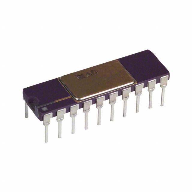
| 描述 | IC 4-20MA I-TRANSMITTER 14-SOIC电流灵敏放大器 4-20mA Crnt Trnsmtr w/Sensor Exc & Lin |
| 产品分类 | |
| 品牌 | Texas Instruments |
| 产品手册 | |
| 产品图片 |
|
| rohs | 符合RoHS无铅 / 符合限制有害物质指令(RoHS)规范要求 |
| 产品系列 | 放大器 IC,电流灵敏放大器,Texas Instruments XTR105U- |
| 数据手册 | |
| 产品型号 | XTR105U |
| 产品目录页面 | |
| 产品种类 | 电流灵敏放大器 |
| 供应商器件封装 | 14-SO |
| 共模抑制比—最小值 | 100 dB |
| 包装 | 管件 |
| 单位重量 | 129.400 mg |
| 单电源电压 | 7.5 V to 36 V |
| 商标 | Texas Instruments |
| 安装类型 | 表面贴装 |
| 安装风格 | SMD/SMT |
| 封装 | Tube |
| 封装/外壳 | 14-SOIC(0.154",3.90mm 宽) |
| 封装/箱体 | SOIC-14 |
| 工厂包装数量 | 50 |
| 接口 | 3 线 |
| 最大工作温度 | + 85 C |
| 最小工作温度 | - 40 C |
| 标准包装 | 50 |
| 电流-电源 | 20mA |
| 电源电压-最大 | 36 V |
| 电源电压-最小 | 7.5 V |
| 电源电流 | 0.8 mA |
| 类型 | 电流发送器 |
| 系列 | XTR105 |
| 输入类型 | 差分 |
| 输入补偿电压 | 0.1 mV |
| 输出类型 | 电压 |


- 商务部:美国ITC正式对集成电路等产品启动337调查
- 曝三星4nm工艺存在良率问题 高通将骁龙8 Gen1或转产台积电
- 太阳诱电将投资9.5亿元在常州建新厂生产MLCC 预计2023年完工
- 英特尔发布欧洲新工厂建设计划 深化IDM 2.0 战略
- 台积电先进制程称霸业界 有大客户加持明年业绩稳了
- 达到5530亿美元!SIA预计今年全球半导体销售额将创下新高
- 英特尔拟将自动驾驶子公司Mobileye上市 估值或超500亿美元
- 三星加码芯片和SET,合并消费电子和移动部门,撤换高东真等 CEO
- 三星电子宣布重大人事变动 还合并消费电子和移动部门
- 海关总署:前11个月进口集成电路产品价值2.52万亿元 增长14.8%


PDF Datasheet 数据手册内容提取
XTR105 XTR105 XTR105 SBOS061B – FEBRUARY 1997 – REVISED AUGUST 2004 4-20mA CURRENT TRANSMITTER with Sensor Excitation and Linearization FEATURES APPLICATIONS (cid:1) LOW UNADJUSTED ERROR (cid:1) INDUSTRIAL PROCESS CONTROL (cid:1) TWO PRECISION CURRENT SOURCES: 800µA each (cid:1) FACTORY AUTOMATION (cid:1) LINEARIZATION (cid:1) SCADA REMOTE DATA ACQUISITION (cid:1) 2- OR 3-WIRE RTD OPERATION (cid:1) REMOTE TEMPERATURE AND PRESSURE (cid:1) LOW OFFSET DRIFT: 0.4µV/°C TRANSDUCERS (cid:1) LOW OUTPUT CURRENT NOISE: 30nA PP (cid:1) HIGH PSR: 110dB minimum Pt100 NONLINEARITY CORRECTION USING XTR105 (cid:1) HIGH CMR: 86dB minimum 5 (cid:1) WIDE SUPPLY RANGE: 7.5V to 36V 4 (cid:1) DIP-14 AND SO-14 PACKAGES %) 3 DESCRIPTION y ( Uncorrected arit 2 RTD Nonlinearity e n The XTR105 is a monolithic 4-20mA, 2-wire current transmit- nli No 1 ter with two precision current sources. It provides complete Corrected Nonlinearity current excitation for platinum RTD temperature sensors and 0 bridges, instrumentation amplifiers, and current output cir- cuitry on a single integrated circuit. −1 −200°C +850°C Versatile linearization circuitry provides a 2nd-order correc- Process Temperature (°C) tion to the RTD, typically achieving a 40:1 improvement in linearity. I = 0.8mA Instrumentation amplifier gain can be configured for a wide R range of temperature or pressure measurements. Total un- IR = 0.8mA VLIN adjusted error of the complete current transmitter is low V REG 7.5V to 36V enough to permit use without adjustment in many applica- + V PS tions. This includes zero output current drift, span drift, and nonlinearity. The XTR105 operates on loop power-supply 4-20 mA voltages down to 7.5V. RTD RG XTR105 VO The XTR105 is available in DIP-14 and SO-14 surface- mount packages and is specified for the –40°C to +85°C R L industrial temperature range. – Please be aware that an important notice concerning availability, standard warranty, and use in critical applications of Texas Instruments semiconductor products and disclaimers thereto appears at the end of this data sheet. All trademarks are the property of their respective owners. PRODUCTION DATA information is current as of publication date. Copyright © 1997-2004, Texas Instruments Incorporated Products conform to specifications per the terms of Texas Instruments standard warranty. Production processing does not necessarily include testing of all parameters. www.ti.com
ABSOLUTE MAXIMUM RATINGS(1) ELECTROSTATIC Power Supply, V+ (referenced to the IO pin)......................................40V DISCHARGE SENSITIVITY Input Voltage, V , V (referenced to the I pin)....................0V to V+ IN+ IN– O Storage Temperature Range.........................................–55°C to +125°C This integrated circuit can be damaged by ESD. Texas Instru- Lead Temperature (soldering, 10s)...............................................+300°C ments recommends that all integrated circuits be handled with Output Current Limit................................................................Continuous Junction Temperature....................................................................+165°C appropriate precautions. Failure to observe proper handling and installation procedures can cause damage. NOTE: (1) Stresses above those listed under “Absolute Maximum Ratings” may cause permanent damage to the device. Exposure to absolute maximum ESD damage can range from subtle performance degrada- conditions for extended periods may affect device reliability. tion to complete device failure. Precision integrated circuits may be more susceptible to damage because very small parametric changes could cause the device not to meet its published specifications. PACKAGE/ORDERING INFORMATION(1) SPECIFIED PACKAGE TEMPERATURE PACKAGE ORDERING TRANSPORT PRODUCT PACKAGE-LEAD DESIGNATOR RANGE MARKING NUMBER MEDIA, QUANTITY XTR105 DIP-14 N –40°C to +85°C XTR105PA XTR105PA Rails, 25 " " " " XTR105P XTR105P Rails, 25 XTR105 SO-14 Surface-Mount D –40°C to +85°C XTR105UA XTR105UA Rails, 58 " " " " XTR105UA XTR105UA/2K5 Tape and Reel, 2500 XTR105 SO-14 Surface-Mount D –40°C to +85°C XTR105U XTR105U Rails, 58 " " " " XTR105U XTR105U/2K5 Tape and Reel, 2500 NOTE: (1) For the most current package and ordering information, see the Package Option Addendum located at the end of this data sheet. FUNCTIONAL BLOCK DIAGRAM PIN CONFIGURATION Top View DIP and SO VLIN IR1 12 1 IR2 14 VREG V+ 800µA 800µA 11 I 1 14 I R1 R2 10 VI+N 13 5.1V VI–N 2 13 VI+N 4 R 3 12 V G LIN R1kLΩIN 100µA 9B Q1 RG 4 11 VREG RG NC 5 10 V+ 3 E I = 100µA +VIN 8 IRET 6 9 B (Base) VI–N 2 RG I 7 8 E (Emitter) O 975Ω 25Ω NC = No Internal Connection 7 IO = 4mA + VIN •( R4 0 G ) 6 IRET XTR105 2 www.ti.com SBOS061B
ELECTRICAL CHARACTERISTICS At T = +25°C, V+= 24V, and TIP29C external transistor, unless otherwise noted. A XTR105P, U XTR105PA, UA PARAMETER CONDITIONS MIN TYP MAX MIN TYP MAX UNITS OUTPUT Output Current Equation I = V • (40/R ) + 4mA, V in Volts, R in Ω A Output Current, Specified Range 4 O IN G 20 IN ✻ G ✻ mA Over-Scale Limit 24 27 30 ✻ ✻ ✻ mA Under-Scale Limit I = 0V 1.8 2.2 2.6 ✻ ✻ ✻ mA REG ZERO OUTPUT(1) V = 0V, R = ∞ 4 ✻ mA IN G Initial Error ±5 ±25 ✻ ±50 µA vs Temperature ±0.07 ±0.5 ✻ ±0.9 µA/°C vs Supply Voltage, V+ V+ = 7.5V to 36V 0.04 0.2 ✻ ✻ µA/V vs Common-Mode Voltage V = 1.25V to 3.5V(2) 0.02 ✻ µA/V CM vs V Output Current 0.3 ✻ µA/mA REG Noise, 0.1Hz to 10Hz 0.03 ✻ µA PP SPAN Span Equation (transconductance) S = 40/R ✻ A/V G Initial Error(3) Full-Scale (V ) = 50mV ±0.05 ±0.2 ✻ ±0.4 % IN vs Temperature(3) ±3 ±25 ✻ ✻ ppm/°C Nonlinearity, Ideal Input(4) Full-Scale (V ) = 50mV 0.003 0.01 ✻ ✻ % IN INPUT(5) Offset Voltage V = 2V ±50 ±100 ✻ ±250 µV CM vs Temperature ±0.4 ±1.5 ✻ ±3 µV/°C vs Supply Voltage, V+ V+ = 7.5V to 36V ±0.3 ±3 ✻ ✻ µV/V vs Common-Mode Voltage, V = 1.25V to 3.5V(2) ±10 ±50 ✻ ±100 µV/V CM RTI (CMRR) Common-Mode Input Range(2) 1.25 3.5 ✻ ✻ V Input Bias Current 5 25 ✻ 50 nA vs Temperature 20 ✻ pA/°C Input Offset Current ±0.2 ±3 ✻ ±10 nA vs Temperature 5 ✻ pA/°C Impedance, Differential 0.1 || 1 ✻ GΩ || pF Common-Mode 5 || 10 ✻ GΩ || pF Noise, 0.1Hz to 10Hz 0.6 ✻ µV PP CURRENT SOURCES V = 2V(6) O Current 800 ✻ µA Accuracy ±0.05 ±0.2 ✻ ±0.4 % vs Temperature ±15 ±35 ✻ ±75 ppm/°C vs Power Supply, V+ V+ = 7.5V to 36V ±10 ±25 ✻ ✻ ppm/V Matching ±0.02 ±0.1 ✻ ±0.2 % vs Temperature ±3 ±15 ✻ ±30 ppm/°C vs Power Supply, V+ V+ = 7.5V to 36V 1 10 ✻ ✻ ppm/V Compliance Voltage, Positive (V+)– 3 (V+) – 2.5 ✻ ✻ V Negative(2) 0 –0.2 ✻ ✻ V Output Impedance 150 ✻ MΩ Noise, 0.1Hz to 10Hz 0.003 ✻ µA PP V (2) 5.1 ✻ V REG Accuracy ±0.02 ±0.1 ✻ ✻ V vs Temperature ±0.2 ✻ mV/°C vs Supply Voltage, V+ 1 ✻ mV/V Output Current ±1 ✻ mA Output Impedance 75 ✻ Ω LINEARIZATION R (internal) 1 ✻ kΩ LIN Accuracy ±0.2 ±0.5 ✻ ±1 % vs Temperature ±25 ±100 ✻ ✻ ppm/°C POWER SUPPLY Specified +24 ✻ V Voltage Range +7.5 +36 ✻ ✻ V TEMPERATURE RANGE Specification, T to T –40 +85 ✻ ✻ °C MIN MAX Operating –55 +125 ✻ ✻ °C Storage –55 +125 ✻ ✻ °C Thermal Resistance, θ JA DIP-14 80 ✻ °C/W SO-14 Surface-Mount 100 ✻ °C/W ✻ Specification same as XTR105P and XTR105U. NOTES:(1) Describes accuracy of the 4mA low-scale offset current. Does not include input amplifier effects. Can be trimmed to zero. (2) Voltage measured with respect to I pin. RET (3) Does not include initial error or TCR of gain-setting resistor, R . G (4) Increasing the full-scale input range improves nonlinearity. (5) Does not include Zero Output initial error. (6) Current source output voltage with respect to I pin. RET XTR105 3 SBOS061B www.ti.com
TYPICAL CHARACTERISTICS At T = +25°C and V+ = 24V, unless otherwise noted. A TRANSCONDUCTANCE vs FREQUENCY STEP RESPONSE 50 mA/V) 40 RG = 500Ω RG = 125Ω 20mA RG = 2kΩ g o L ce (20 30 A/div RG = 125Ω n m ucta 20 R = 2kΩ 4 d G n co 4mA ns 10 a Tr 0 100 1k 10k 100k 1M 25µs/div Frequency (Hz) COMMON-MODE REJECTION vs FREQUENCY POWER-SUPPLY REJECTION vs FREQUENCY 110 140 Full-Scale Input = 50mV 100 e Rejection (dB) 987000 RG = 125Ω Rejection (dB) 11208000 RG = 2kΩ RG = 125Ω mmon-Mod 654000 RG = 2kΩ wer Supply 6400 o o C P 20 30 20 0 10 100 1k 10k 100k 1M 10 100 1k 10k 100k 1M Frequency (Hz) Frequency (Hz) OVER-SCALE CURRENT vs TEMPERATURE UNDER-SCALE CURRENT vs TEMPERATURE 29 2.40 With External Transistor 28 mA) mA) 2.35 Over-Scale Current ( 222765 V+ = 36V V+ = 24V V+ = 7.5V Under-Scale Current ( 222...322050 24 V+ = 7.5V to 36V 23 2.15 –75 –50 –25 0 25 50 75 100 125 –75 –50 –25 0 25 50 75 100 125 Temperature (°C) Temperature (°C) XTR105 4 www.ti.com SBOS061B
TYPICAL CHARACTERISTICS (Cont.) At T = +25°C and V+= 24V, unless otherwise noted. A INPUT VOLTAGE AND CURRENT ZERO OUTPUT AND REFERENCE NOISE DENSITY vs FREQUENCY CURRENT NOISE vs FREQUENCY 10k 10k 10k Hz) Hz) Zero Output Current √oise (nV/ 1k 1k √oise (fA/ √A/Hz) 1k N N p Voltage 100 Current Noise 100 Current Noise ( 100 Input Input Reference Current Voltage Noise 10 10 10 1 10 100 1k 10k 100k 1 10 100 1k 10k 100k Frequency (Hz) Frequency (Hz) INPUT BIAS AND OFFSET CURRENT ZERO OUTPUT CURRENT ERROR vs TEMPERATURE vs TEMPERATURE 25 4 nA) A) 2 ent ( 20 or (µ 0 Offset Curr 15 +IB Current Err ––24 Bias and 10 –IB o Output ––68 put 5 I Zer –10 n OS I 0 –12 –75 –50 –25 0 25 50 75 100 125 –75 –50 –25 0 25 50 75 100 125 Temperature (°C) Temperature (°C) INPUT OFFSET VOLTAGE DRIFT ZERO OUTPUT DRIFT PRODUCTION DISTRIBUTION PRODUCTION DISTRIBUTION 50 40 Typical Production Distribution 45 Typical Production Distribution of Packaged Units. 35 of Packaged Units. 40 %) 35 %) 30 Units ( 30 Units ( 25 Percent of 221505 Percent of 211050 10 0.1% 0.02% 5 5 0 0 0.2 0.4 0.6 0.8 1.0 1.2 1.4 1.6 1.8 2.0 2.2 2.4 2.6 2.8 3.0 025050075100125150175200225250275300325350375400425450475500 Input Offset Voltage Drift (µV/°C) 0.0.0.0.0.0.0.0.0.0.0.0.0.0.0.0.0.0.0.0. Zero Output Drift (µA/°C) XTR105 5 SBOS061B www.ti.com
TYPICAL CHARACTERISTICS (Cont.) At T = +25°C and V+= 24V, unless otherwise noted. A CURRENT SOURCE DRIFT CURRENT SOURCE MATCHING PRODUCTION DISTRIBUTION DRIFT PRODUCTION DISTRIBUTION 40 80 Typical Production Distribution Typical Production Distribution 35 of Packaged Units. 70 of Packaged Units. I AND I Included. %) 30 R1 R2 %) 60 nits ( 25 nits ( 50 U U of 20 of 40 ent 15 ent 30 erc erc P 10 P 20 0.04% 0.01% 0.07% 0.02% 5 10 0 0 5 0 5 0 5 0 5 0 5 0 5 0 5 0 5 2 4 6 8 0 2 4 6 8 0 2 4 6 8 0 1 1 2 2 3 3 4 4 5 5 6 6 7 7 1 1 1 1 1 2 2 2 2 2 3 Current Source Drift (ppm/°C) Current Source Matching Drift (ppm/°C) REFERENCE CURRENT ERROR V OUTPUT VOLTAGE vs V OUTPUT CURRENT vs TEMPERATURE REG REG 5.35 +0.05 125°C 5.30 %) 0 V Output Voltage (V)REG 5555....22115050 –55°C 25°C NZeOrTo EO: uAtpbuotv eD e1gmraAd,es eference Current Error ( –––000...011505 R 5.05 5.00 –0.20 –1.0 –0.5 0 0.5 1.0 1.5 2.0 –75 –50 –25 0 25 50 75 100 125 V Output Current (mA) Temperature (°C) REG XTR105 6 www.ti.com SBOS061B
APPLICATION INFORMATION The transfer function through the complete instrumentation amplifier and voltage-to-current converter is: Figure 1 shows the basic connection diagram for the XTR105. I = 4mA + V • (40/R ) The loop power supply, V , provides power for all circuitry. O IN G PS (V in volts, R in ohms) Output loop current is measured as a voltage across the IN G series load resistor, R . where V is the differential input voltage. L IN Two matched 0.8mA current sources drive the RTD and As evident from the transfer function, if no R is used the G zero-setting resistor, R . The instrumentation amplifier input gain is zero and the output is simply the XTR105’s zero Z of the XTR105 measures the voltage difference between the current. The value of R varies slightly for 2-wire RTD and 3- G RTD and R . The value of R is chosen to be equal to the wire RTD connections with linearization. R can be calcu- Z Z G resistance of the RTD at the low-scale (minimum) measure- lated from the equations given in Figure 1 (2-wire RTD ment temperature. R can be adjusted to achieve 4mA output connection) and Table I (3-wire RTD connection). Z at the minimum measurement temperature to correct for The I pin is the return path for all current from the current RET input offset voltage and reference current mismatch of the sources and V . The I pin allows any current used in REG RET XTR105. external circuitry to be sensed by the XTR105 and to be R provides an additional voltage drop to bias the inputs of included in the output current without causing an error. CM the XTR105 within their common-mode input range. RCM The VREG pin provides an on-chip voltage source of approxi- should be bypassed with a 0.01µF capacitor to minimize mately 5.1V and is suitable for powering external input common-mode noise. Resistor RG sets the gain of the instru- circuitry (refer to Figure 6). It is a moderately accurate mentation amplifier according to the desired temperature voltage reference—it is not the same reference used to set range. RLIN1 provides 2nd-order linearization correction to the the 800µA current references. VREG is capable of sourcing RTD, typically achieving a 40:1 improvement in linearity. An approximately 1mA of current. Exceeding 1mA may affect additional resistor is required for 3-wire RTD connections the 4mA zero output. (see Figure 3). I = 0.8mA R Possible choices for Q (see text). 1 IR = 0.8mA TYPE PACKAGE 2N4922 TO-225 TIP29C TO-220 TIP31C TO-220 12 13 VI+VNLIN IR11 IR214V 11 10 7.5V to 36V REG V+ I 4 O R G 4-20 mA 9 R(G2) XTR105 B Q1 0.01µF V O 3 + RLIN1(3) RG E 8 RL VPS IO – 2 VI–N 7 I RET RTD RZ(1) 6 I O = 4mA + VIN • ( 4R 0 ) G NOTES: (1) R = RTD resistance at minimum measured temperature. Z RCM = 1kΩ (2)RG = 2R1(R2 R+R Z–) R– 4(R2RZ) 2 1 R (R – R) 0.01µF (3)R = LIN 2 1 LIN1 2(2R – R – R ) 1 2 Z where R = RTD Resistance at (T + T )/2 1 MIN MAX R = RTD Resistance at T 2 MAX R = 1kΩ (Internal) LIN FIGURE 1. Basic 2-Wire RTD Temperature Measurement Circuit with Linearization. XTR105 7 SBOS061B www.ti.com
MEASUREMENT TEMPERATURE SPAN ∆T (°C) T 100°C 200°C 300°C 400°C 500°C 600°C 700°C 800°C 900°C 1000°C MIN –200°C 18.7/86.6 18.7/169 18.7/255 18.7/340 18.7/422 18.7/511 18.7/590 18.7/665 18.7/750 18.7/845 15000 9760 8060 6650 5620 4750 4020 3480 3090 2740 16500 11500 10000 8870 7870 7150 6420 5900 5360 4990 –100°C 60.4/80.6 60.4/162 60.4/243 60.4/324 60.4/402 60.4/487 60.4/562 60.4/649 60.4/732 27400 15400 10500 7870 6040 4990 4220 3570 3090 29400 17800 13000 10200 8660 7500 6490 5900 5360 0°C 100/78.7 100/158 100/237 100/316 100/392 100/475 100/549 100/634 33200 16200 10500 7680 6040 4870 4020 3480 35700 18700 13000 10000 8250 7150 6340 5620 100°C 137/75 137/150 137/226 137/301 137/383 137/453 137/536 31600 15400 10200 7500 5760 4750 3920 R /R Z G 34000 17800 12400 9760 8060 6810 6040 R LIN1 200°C 174/73.2 174/147 174/221 174/294 174/365 174/442 RLIN2 30900 15000 9760 7150 5620 4530 33200 17400 12100 9310 7680 6490 300°C 210/71.5 210/143 210/215 210/287 210/357 30100 14700 9530 6980 5360 32400 16500 11500 8870 7320 NOTE: The values listed in this table are 1% resistors (in Ω). 400°C 249/68.1 249/137 249/205 249/274 Exact values may be calculated from the following equa- 28700 14000 9090 6650 tions: 30900 16200 11000 8450 500°C 280/66.5 280/133 280/200 RZ = RTD resistance at minimum measured temperature. 28000 13700 8870 2(R –R )(R –R ) 30100 15400 10500 RG= 2(RZ–R1) Z 2 1 600°C 316/64.9 313/130 26700 13000 R = RLIN(R2–R1) 28700 14700 LIN1 2(2R –R –R ) 1 2 Z 700°C 348/61.9 26100 (R +R )(R –R) 27400 RLIN2= 2L(IN2R –GR –2R )1 1 2 Z 800°C 374/60.4 24900 where: R = RTD resistance at (T + T )/2 26700 1 MIN MAX R = RTD resistance at T 2 MAX R = 1kΩ (Internal) LIN EXAMPLE: The measurement range is –100°C to +200°C for a 3-wire Pt100 RTD connection. Determine the values for R , R , R , and R . Look up the values S G LIN1 LIN2 from the chart or calculate the values according to the equations provided. METHOD 1: TABLE LOOK UP For T = –100°C and ∆T = –300°C, the 1% values are: MIN R = 60.4Ω R = 10.5kΩ Z LIN1 R = 243Ω R = 13kΩ G LIN2 METHOD 2: CALCULATION Calculation of Pt100 Resistance Values Step 1: Determine R , R, and R. (according to DIN IEC 751) Z 1 2 R is the RTD resistance at the minimum measured temperature,T = –100°C. (Equation 1) Temperature range from –200°C to 0°C: Z MIN Using Equation 1 at right gives RZ = 60.25Ω (1% value is 60.4Ω). R(T) = 100 [1 + 3.90802 • 10–3 • T – 0.5802 • 10–6 • T2 – 4.27350 • 10–12 (T – 100) T3] R is the RTD resistance at the maximum measured temperature, T = 200°C. 2 MAX Using Equation 2 at right gives R2 = 175.84Ω. (Equation 2) Temperature range from 0°C to +850°C: R is the RTD resistance at the midpoint measured temperature, R = 100 (1 + 3.90802 • 10–3 • T – 0.5802 • 10–6 • T) 1 (T) 2 T = (T + T )/2 = 50°C. R is NOT the average of R and R. MID MIN MAX 1 Z 2 Using Equation 2 at right gives R = 119.40Ω. where: R is the resistance in Ω at temperature T. 1 (T) T is the temperature in °C. Step 2: Calculate R , R , and R using equations above. G LIN1 LIN2 R = 242.3Ω (1% value is 243Ω) NOTE: Most RTD manufacturers provide reference tables for RG = 10.413kΩ (1% value is 10.5kΩ) resistance values at various temperatures. LIN1 R = 12.936kΩ (1% value is 13kΩ) LIN2 TABLE I. R , R , R , and R Standard 1% Resistor Values for 3-Wire Pt100 RTD Connection with Linearization. Z G LIN1 LIN2 A negative input voltage, V , will cause the output current to Increasingly positive input voltage (greater than the full-scale IN be less than 4mA. Increasingly negative V will cause the input) will produce increasing output current according to the IN output current to limit at approximately 2.2mA. Refer to the transfer function, up to the output current limit of approxi- typical characteristic Under-Scale Current vs Temperature. mately 27mA. Refer to the typical characteristic Over-Scale Current vs Temperature. XTR105 8 www.ti.com SBOS061B
EXTERNAL TRANSISTOR It is recommended to design for V+ equal or greater than 7.5V with loop currents up to 30mA to allow for out-of-range Transistor Q conducts the majority of the signal-dependent 1 input conditions. 4-20mA loop current. Using an external transistor isolates the majority of the power dissipation from the precision input The low operating voltage (7.5V) of the XTR105 allows and reference circuitry of the XTR105, maintaining excellent operation directly from personal computer power supplies accuracy. (12V ±5%). When used with the RCV420 current loop re- ceiver (see Figure 7), the load resistor voltage drop is limited Since the external transistor is inside a feedback loop, its to 3V. characteristics are not critical. Requirements are: V = 45V CEO min, β = 40 min, and P = 800mW. Power dissipation D requirements may be lower if the loop power-supply voltage ADJUSTING INITIAL ERRORS is less than 36V. Some possible choices for Q1 are listed in Many applications require adjustment of initial errors. Input Figure 1. offset and reference current mismatch errors can be cor- The XTR105 can be operated without this external transis- rected by adjustment of the zero resistor, R . Adjusting the Z tor, however, accuracy will be somewhat degraded due to gain-setting resistor, R , corrects any errors associated with G the internal power dissipation. Operation without Q is not gain. 1 recommended for extended temperature ranges. A resistor (R = 3.3kΩ) connected between the IRET pin and the E 2- AND 3-WIRE RTD CONNECTIONS (emitter) pin may be needed for operation below 0°C with- In Figure 1, the RTD can be located remotely simply by out Q to ensure the full 20mA full-scale output, especially 1 extending the two connections to the RTD. With this remote with V+ near 7.5V. 2-wire connection to the RTD, line resistance will introduce error. This error can be partially corrected by adjusting the values of R ,R , and R . Z G LIN1 A better method for remotely located RTDs is the 3-wire RTD connection (see Figure 3). This circuit offers improved accu- racy. R ’s current is routed through a third wire to the RTD. 10 Z Assuming line resistance is equal in RTD lines 1 and 2, this V+ produces a small common-mode voltage that is rejected by 8 E the XTR105. A second resistor, R , is required for linear- LIN2 ization. XTR105 0.01µF Note that although the 2-wire and 3-wire RTD connection circuits are very similar, the gain-setting resistor, R , has G I slightly different equations: O 7 IRET 2-wire: RG= 2R1(R2+RZ)–4(R2RZ) R –R 6 2 1 For operation without an external transistor, connect a 3.3kΩ 2(R –R )(R –R ) RQ = 3.3kΩ rSeeseis tteoxr tb feotrw deisecnu psisni o6n a nd pin 8. 3-wire: RG= 2 R2Z–R11 Z of performance. where: R = RTD resistance at T Z MIN R = RTD resistance at (T + T )/2 1 MIN MAX FIGURE 2. Operation Without an External Transistor. R = RTD resistance at T 2 MAX To maintain good accuracy, at least 1% (or better) resistors LOOP POWER SUPPLY should be used for R . Table I provides standard 1% R G G The voltage applied to the XTR105, V+, is measured with resistor values for a 3-wire Pt100 RTD connection with respect to the I connection, pin 7. V+ can range from 7.5V linearization. O to 36V. The loop-supply voltage, V , will differ from the PS voltage applied to the XTR105 according to the voltage drop LINEARIZATION on the current sensing resistor, R (plus any other voltage L RTD temperature sensors are inherently (but predictably) drop in the line). nonlinear. With the addition of one or two external resistors, If a low loop-supply voltage is used, R (including the loop L R and R , it is possible to compensate for most of this wiring resistance) must be made a relatively low value to LIN1 LIN2 nonlinearity resulting in 40:1 improvement in linearity over assure that V+ remains 7.5V or greater for the maximum loop the uncompensated output. current of 20mA: See Figure 1 for a typical 2-wire RTD application with R max=(V+)–7.5V–R linearization. Resistor RLIN1 provides positive feedback and L 20mA WIRING controls linearity correction. R is chosen according to the LIN1 desired temperature range. An equation is given in Figure 1. XTR105 9 SBOS061B www.ti.com
In 3-wire RTD connections, an additional resistor, R , is ERROR ANALYSIS LIN2 required. As with the 2-wire RTD application, R provides LIN1 See Table II for how to calculate the effect various error positive feedback for linearization. R provides an offset LIN2 sources have on circuit accuracy. A sample error calculation canceling current to compensate for wiring resistance en- for a typical RTD measurement circuit (Pt100 RTD, 200°C countered in remotely located RTDs. R and R are LIN1 LIN2 measurement span) is provided. The results reveal the chosen such that their currents are equal. This makes the XTR105’s excellent accuracy, in this case 1.1% unadjusted. voltage drop in the wiring resistance to the RTD a common- Adjusting resistors R and R for gain and offset errors G Z mode signal that is rejected by the XTR105. The nearest improves circuit accuracy to 0.32%. Note that these are standard 1% resistor values for R and R should be LIN1 LIN2 worst-case errors; ensured maximum values were used in adequate for most applications. Table I provides the 1% the calculations and all errors were assumed to be positive resistor values for a 3-wire Pt100 RTD connection. (additive). The XTR105 achieves performance that is difficult If no linearity correction is desired, the V pin should be left to obtain with discrete circuitry and requires less space. LIN open. With no linearization, R = 2500 • V , where G FS V = full-scale input range. FS OPEN-CIRCUIT PROTECTION The optional transistor Q in Figure 3 provides predictable RTDs 2 behavior with open-circuit RTD connections. It assures that The text and figures thus far have assumed a Pt100 RTD. With if any one of the three RTD connections is broken, the higher resistance RTDs, the temperature range and input XTR105’s output current will go to either its high current limit voltage variation should be evaluated to ensure proper com- (≈ 27mA) or low current limit (≈ 2.2mA). This is easily mon-mode biasing of the inputs. As mentioned earlier, R can detected as an out-of-range condition. CM be adjusted to provide an additional voltage drop to bias the inputs of the XTR105 within their common-mode input range. 12 I 1 O VLIN I 14 RLIN1(1) RLIN2(1) 13 VI+N R1 IR2VRE1G1V1+0 4 R G R(G1) XTR105 B 9 Q1 0.01µF 3 R E G 8 I 2 O VI–N 7 I RET EcrQeaUtAesL alin sem raelsl icsotamnmceosn -hmeroed e RZ(1) 6 IO voltage which is rejected by the XTR105. 2 1 RCM = 1000Ω 0.01µF (R ) (R ) LINE2 LINE1 NOTES: (1) See Table I for resistor equations and RTD 2N2Q222(22) 1o%utp vuatl uceusrr.e (n2t) iQf a2n oyp otinoen aRl.T PDr ocvoindnees cptiroend iicst able broken: OPEN RTD I TERMINAL O (R ) LINE3 1 ≈ 2.2mA 2 ≈27mA Resistance in this line causes 3 3 ≈2.2mA a small common-mode voltage which is rejected by the XTR105. FIGURE 3. Remotely Located RTDs with 3-Wire Connection. XTR105 10 www.ti.com SBOS061B
SAMPLE ERROR CALCULATION RTD value at 4mA Output (R ): 100Ω RTD MIN RTD Measurement Range: 200°C Ambient Temperature Range (∆T ): 20°C A Supply Voltage Change (∆V+): 5V Common-Mode Voltage Change (∆CM): 0.1V ERROR SAMPLE (ppm of Full Scale) ERROR SOURCE ERROR EQUATION ERROR CALCULATION(1) UNADJ. ADJUST. INPUT Input Offset Voltage V /(V ) • 106 100µV/(800µA • 0.38Ω/°C • 200°C) • 106 1645 0 OS IN MAX vs Common-Mode CMRR • ∆CM/(V ) • 106 50µV/V • 0.1V/(800µA • 0.38Ω/°C • 200°C) • 106 82 82 IN MAX Input Bias Current I/I • 106 0.025µA/800µA • 106 31 0 B REF Input Offset Current I • R /(V ) • 106 3nA • 100Ω/(800µA • 0.38Ω/°C • 200°C) • 106 5 0 OS RTD MIN IN MAX Total Input Error: 1763 82 EXCITATION Current Reference Accuracy I Accuracy (%)/100% • 106 0.2%/100% • 106 2000 0 REF vs Supply (I vs V+) • ∆V+ 25ppm/V • 5V 125 125 REF Current Reference Matching I Matching (%)/100% • 800µA • 0.1%/100% • 800µA • 100Ω/(800µA • 0.38Ω/°C • 200°C) • 106 1316 0 REF R /(V ) • 106 RTD MIN IN MAX vs Supply (I Matching vs V+) • ∆V+ • 10ppm/V • 5V • 800µA • 100Ω/(800µA • 0.38Ω/°C • 200°C) 66 66 REF R /(V ) RTD MIN IN MAX Total Excitation Error: 3507 191 GAIN Span Span Error (%)/100% • 106 0.2%/100% • 106 2000 0 Nonlinearity Nonlinearity (%)/100% • 106 0.01%/100% • 106 100 100 Total Gain Error: 2100 100 OUTPUT Zero Output (I – 4mA) /16000µA • 106 25µA/16000µA • 106 1563 0 ZERO vs Supply (I vs V+) • ∆V+/16000µA • 106 0.2µA/V • 5V/16000µA • 106 63 63 ZERO Total Output Error: 1626 63 DRIFT (∆T = 20°C) A Input Offset Voltage Drift • ∆T/(V ) • 106 1.5µV/°C • 20°C/(800µA • 0.38Ω/°C • 200°C) • 106 493 493 A IN MAX Input Bias Current (typical) Drift • ∆T/800µA • 106 20pA/°C • 20°C/800µA • 106 0.5 0.5 A Input Offset Current (typical) Drift • ∆T • R /(V ) • 106 5pA/°C • 20°C • 100W/(800µA • 0.38Ω/°C • 200°C) • 106 0.2 0.2 A RTD MIN IN MAX Current Reference Accuracy Drift • ∆T 35ppm/°C • 20°C 700 700 A Current Reference Matching Drift • ∆T • 800µA • R /(V ) 15ppm/°C • 20°C • 800µA • 100Ω/(800µA • 0.38Ω/°C • 200°C) 395 395 A RTD MIN IN MAX Span Drift • ∆T 25ppm/°C • 20°C 500 500 A Zero Output Drift • ∆T/16000µA • 106 0.5µA/°C • 20°C/16000µA • 106 626 626 A Total Drift Error: 2715 2715 NOISE (0.1Hz to 10Hz, typ) Input Offset Voltage v/(V ) • 106 0.6µV/(800µA • 0.38Ω/°C • 200°C) • 106 10 10 n IN MAX Current Reference I Noise • R /(V ) • 106 3nA • 100Ω/(800µA • 0.38Ω/°C • 200°C) • 106 5 5 REF RTD MIN IN MAX Zero Output I Noise/16000µA • 106 0.03µA/16000µA • 106 2 2 ZERO Total Noise Error: 17 17 NOTE (1): All errors are min/max and referred to input unless otherwise stated. TOTAL ERROR: 11728 3168 (1.17%) (0.32%) TABLE II. Error Calculation. XTR105 11 SBOS061B www.ti.com
REVERSE-VOLTAGE PROTECTION Most surge protection zener diodes have a diode character- istic in the forward direction that will conduct excessive The XTR105’s low compliance rating (7.5V) permits the use current, possibly damaging receiving-side circuitry if the loop of various voltage protection methods without compromising connections are reversed. If a surge protection diode is used, operating range. Figure 4 shows a diode bridge circuit that a series diode or diode bridge should be used for protection allows normal operation even when the voltage connection against reversed connections. lines are reversed. The bridge causes a two diode drop (approximately 1.4V) loss in loop-supply voltage. This results in a compliance voltage of approximately 9V—satisfactory RADIO FREQUENCY INTERFERENCE for most applications. If a 1.4V drop in loop supply is too The long wire lengths of current loops invite radio frequency much, a diode can be inserted in series with the loop-supply (RF) interference. RF can be rectified by the sensitive input voltage and the V+ pin. This protects against reverse output circuitry of the XTR105 causing errors. This generally ap- connection lines with only a 0.7V loss in loop-supply voltage. pears as an unstable output current that varies with the position of loop supply or input wiring. SURGE PROTECTION If the RTD sensor is remotely located, the interference may Remote connections to current transmitters can sometimes be enter at the input terminals. For integrated transmitter as- subjected to voltage surges. It is prudent to limit the maximum semblies with short connections to the sensor, the interfer- surge voltage applied to the XTR105 to as low as practical. ence more likely comes from the current loop connections. Various zener diodes and surge clamping diodes are specially Bypass capacitors on the input reduce or eliminate this input designed for this purpose. Select a clamp diode with as low a interference. Connect these bypass capacitors to the I RET voltage rating as possible for best protection. For example, a terminal (see Figure 5). Although the dc voltage at the I RET 36V protection diode will assure proper transmitter operation terminal is not equal to 0V (at the loop supply, V ), this PS at normal loop voltages, yet will provide an appropriate level circuit point can be considered the transmitter’s “ground.” of protection against voltage surges. Characterization tests on The 0.01µF capacitor connected between V+ and I may O three production lots showed no damage to the XTR105 within help minimize output interference. loop-supply voltages up to 65V. NOTE: (1) Zener Diode 36V: 1N4753A or General Semiconductor TransorbTM 1N6286A. Use lower voltage zener diodes with loop-power supply 10 voltages less than 30V for increased protection. V+ See the Surge Protection section. 0.01µF B D(1) 1N4148 XTR105 9 1 Diodes Maximum V must be PS less than minimum E R V voltage rating of zener 8 L PS diode. I O The diode bridge causes 7 I a 1.4V loss in loop-supply RET voltage. 6 FIGURE 4. Reverse Voltage Operation and Over-Voltage Surge Protection. XTR105 12 www.ti.com SBOS061B
12 1 1kΩ 13 VI+VNLIN IR1 IR214V 11 10 REG V+ 4 R G R R LIN1 LIN2 9 RG XTR105 B 0.01µF 3 R E G 8 I 1kΩ 2 VI–N O7 I RET R Z 6 0.01µF 0.01µF RTD (1) R CM 0.01µF NOTE: (1) Bypass capacitors can be connected to either the I pin or the I pin. RET O FIGURE 5. Input Bypassing Technique with Linearization. I < 1mA REG 5V 12 V+ V 1 Type J OPA1/22335 13 VLI+INN IR1 IR214V 11 10 REG V+ 10RkFΩ 4 RG R412Ω 10RkFΩ R12G50Ω XTR105 B 9 3 R E G 8 I O 1kΩ 1/2 2 VI–N 7 OPA2335 I RET I = 4mA + (V+ – V–)40 50Ω V– 6 O IN IN RG 25Ω R = 1250Ω CM 2R (G = 1 + F = 50) R FIGURE 6. Thermocouple Low Offset, Low Drift Loop Measurement with Diode Cold Junction Compensation. XTR105 13 SBOS061B www.ti.com
12 1 1N4148 13 VI+VNLIN IR1 IR214V 11 10 +12V REG V+ 4 1µF R G R57L6IN01Ω R40G2Ω XTR105 B 9 Q1 0.01µF 1610 11 3 E 8 3 12 R G 15 VO = 0 to 5V 2 VI–N IO7 2 RCV420 13 14 Pt100 IRET 5 10600°C0° tCo RTD 1R3Z7Ω 6 IO = 4mA – 20mA 4 1µF –12V R = 1kΩ CM NOTE: A 2-wire RTD connection is shown. For remotely located RTDs, a 3-wire RTD conection is recommended. 0.01µF R becomes 383Ω, R is 8060Ω. See Figure 3 and G LIN2 Table I. FIGURE 7. ±12V Powered Transmitter/Receiver Loop. 12 RLIN1 RLIN2 13 VI+NVLINIR11 IR214VRE1G1V+10 1N4148 1µF +15V Isolated Power 4 RG 1µF 0 from PWS740 RG XTR105 B 9 Q1 0.01µF 1610 –15V 3 E 8 3 1112 RG 15 1 V+ IO RCV420 14 15 9 RZ 2 VI–NIRET 7 2 4 5 13 ISO122 10 87 0 V– O5V 6 IO = 4mA – 20mA 2 16 RTD NOTE: A 3-wire RTD connection is shown. V– For a 2-wire RTD connection eliminate RLIN2. RCM = 1kΩ 0.01µF FIGURE 8. Isolated Transmitter/Receiver Loop. XTR105 14 www.ti.com SBOS061B
1.6mA 12 1 V LIN 14 I 13 VI+N R1 IR2 V 11 10 REG V+ 4 R G 9 RG XTR105 B 3 8 R E G 2 VI–N 7 I RET 6 R = 1kΩ(1) CM NOTE: (1) Use R to adjust the CM common-mode voltage to within 1.25V to 3.5V. FIGURE 9. Bridge Input, Current Excitation. XTR105 15 SBOS061B www.ti.com
PACKAGE OPTION ADDENDUM www.ti.com 6-Feb-2020 PACKAGING INFORMATION Orderable Device Status Package Type Package Pins Package Eco Plan Lead/Ball Finish MSL Peak Temp Op Temp (°C) Device Marking Samples (1) Drawing Qty (2) (6) (3) (4/5) XTR105P ACTIVE PDIP N 14 25 Green (RoHS NIPDAU N / A for Pkg Type -40 to 85 XTR105P & no Sb/Br) A XTR105PA ACTIVE PDIP N 14 25 Green (RoHS NIPDAU N / A for Pkg Type -40 to 85 XTR105P & no Sb/Br) A XTR105U ACTIVE SOIC D 14 50 Green (RoHS NIPDAU Level-3-260C-168 HR -40 to 85 XTR105U & no Sb/Br) XTR105UA ACTIVE SOIC D 14 50 Green (RoHS NIPDAU Level-3-260C-168 HR -40 to 85 XTR105U & no Sb/Br) A XTR105UA/2K5 ACTIVE SOIC D 14 2500 Green (RoHS NIPDAU Level-3-260C-168 HR -40 to 85 XTR105U & no Sb/Br) A (1) The marketing status values are defined as follows: ACTIVE: Product device recommended for new designs. LIFEBUY: TI has announced that the device will be discontinued, and a lifetime-buy period is in effect. NRND: Not recommended for new designs. Device is in production to support existing customers, but TI does not recommend using this part in a new design. PREVIEW: Device has been announced but is not in production. Samples may or may not be available. OBSOLETE: TI has discontinued the production of the device. (2) RoHS: TI defines "RoHS" to mean semiconductor products that are compliant with the current EU RoHS requirements for all 10 RoHS substances, including the requirement that RoHS substance do not exceed 0.1% by weight in homogeneous materials. Where designed to be soldered at high temperatures, "RoHS" products are suitable for use in specified lead-free processes. TI may reference these types of products as "Pb-Free". RoHS Exempt: TI defines "RoHS Exempt" to mean products that contain lead but are compliant with EU RoHS pursuant to a specific EU RoHS exemption. Green: TI defines "Green" to mean the content of Chlorine (Cl) and Bromine (Br) based flame retardants meet JS709B low halogen requirements of <=1000ppm threshold. Antimony trioxide based flame retardants must also meet the <=1000ppm threshold requirement. (3) MSL, Peak Temp. - The Moisture Sensitivity Level rating according to the JEDEC industry standard classifications, and peak solder temperature. (4) There may be additional marking, which relates to the logo, the lot trace code information, or the environmental category on the device. (5) Multiple Device Markings will be inside parentheses. Only one Device Marking contained in parentheses and separated by a "~" will appear on a device. If a line is indented then it is a continuation of the previous line and the two combined represent the entire Device Marking for that device. (6) Lead/Ball Finish - Orderable Devices may have multiple material finish options. Finish options are separated by a vertical ruled line. Lead/Ball Finish values may wrap to two lines if the finish value exceeds the maximum column width. Addendum-Page 1
PACKAGE OPTION ADDENDUM www.ti.com 6-Feb-2020 Important Information and Disclaimer:The information provided on this page represents TI's knowledge and belief as of the date that it is provided. TI bases its knowledge and belief on information provided by third parties, and makes no representation or warranty as to the accuracy of such information. Efforts are underway to better integrate information from third parties. TI has taken and continues to take reasonable steps to provide representative and accurate information but may not have conducted destructive testing or chemical analysis on incoming materials and chemicals. TI and TI suppliers consider certain information to be proprietary, and thus CAS numbers and other limited information may not be available for release. In no event shall TI's liability arising out of such information exceed the total purchase price of the TI part(s) at issue in this document sold by TI to Customer on an annual basis. Addendum-Page 2
PACKAGE MATERIALS INFORMATION www.ti.com 14-Jul-2012 TAPE AND REEL INFORMATION *Alldimensionsarenominal Device Package Package Pins SPQ Reel Reel A0 B0 K0 P1 W Pin1 Type Drawing Diameter Width (mm) (mm) (mm) (mm) (mm) Quadrant (mm) W1(mm) XTR105UA/2K5 SOIC D 14 2500 330.0 16.4 6.5 9.0 2.1 8.0 16.0 Q1 PackMaterials-Page1
PACKAGE MATERIALS INFORMATION www.ti.com 14-Jul-2012 *Alldimensionsarenominal Device PackageType PackageDrawing Pins SPQ Length(mm) Width(mm) Height(mm) XTR105UA/2K5 SOIC D 14 2500 367.0 367.0 38.0 PackMaterials-Page2
None
None
None
IMPORTANTNOTICEANDDISCLAIMER TI PROVIDES TECHNICAL AND RELIABILITY DATA (INCLUDING DATASHEETS), DESIGN RESOURCES (INCLUDING REFERENCE DESIGNS), APPLICATION OR OTHER DESIGN ADVICE, WEB TOOLS, SAFETY INFORMATION, AND OTHER RESOURCES “AS IS” AND WITH ALL FAULTS, AND DISCLAIMS ALL WARRANTIES, EXPRESS AND IMPLIED, INCLUDING WITHOUT LIMITATION ANY IMPLIED WARRANTIES OF MERCHANTABILITY, FITNESS FOR A PARTICULAR PURPOSE OR NON-INFRINGEMENT OF THIRD PARTY INTELLECTUAL PROPERTY RIGHTS. These resources are intended for skilled developers designing with TI products. You are solely responsible for (1) selecting the appropriate TI products for your application, (2) designing, validating and testing your application, and (3) ensuring your application meets applicable standards, and any other safety, security, or other requirements. These resources are subject to change without notice. TI grants you permission to use these resources only for development of an application that uses the TI products described in the resource. Other reproduction and display of these resources is prohibited. No license is granted to any other TI intellectual property right or to any third party intellectual property right. TI disclaims responsibility for, and you will fully indemnify TI and its representatives against, any claims, damages, costs, losses, and liabilities arising out of your use of these resources. TI’s products are provided subject to TI’s Terms of Sale (www.ti.com/legal/termsofsale.html) or other applicable terms available either on ti.com or provided in conjunction with such TI products. TI’s provision of these resources does not expand or otherwise alter TI’s applicable warranties or warranty disclaimers for TI products. Mailing Address: Texas Instruments, Post Office Box 655303, Dallas, Texas 75265 Copyright © 2020, Texas Instruments Incorporated