ICGOO在线商城 > 集成电路(IC) > 接口 - 传感器和探测器接口 > XTR108EA
 Datasheet下载
- 型号: XTR108EA
- 制造商: Texas Instruments
- 库位|库存: xxxx|xxxx
- 要求:
| 数量阶梯 | 香港交货 | 国内含税 |
| +xxxx | $xxxx | ¥xxxx |
查看当月历史价格
查看今年历史价格
XTR108EA产品简介:
ICGOO电子元器件商城为您提供XTR108EA由Texas Instruments设计生产,在icgoo商城现货销售,并且可以通过原厂、代理商等渠道进行代购。 XTR108EA价格参考。Texas InstrumentsXTR108EA封装/规格:接口 - 传感器和探测器接口, 。您可以下载XTR108EA参考资料、Datasheet数据手册功能说明书,资料中有XTR108EA 详细功能的应用电路图电压和使用方法及教程。
Texas Instruments(德州仪器)的XTR108EA是一款专为传感器和探测器接口设计的信号调理集成电路。它主要用于将低电平的模拟信号(如来自传感器的微弱信号)转换为适合长距离传输的4-20mA电流信号,适用于工业自动化、过程控制等领域。

 应用场景:

1. 工业自动化与过程控制:
   - XTR108EA广泛应用于工业自动化系统中,用于连接各种传感器(如温度、压力、流量等传感器)。它能够将传感器输出的微弱电压信号转换为标准的4-20mA电流信号,便于在恶劣的工业环境中进行远距离传输,同时具有较强的抗干扰能力。

2. 压力传感器接口:
   - 在压力测量系统中,XTR108EA可以与压阻式或电容式压力传感器配合使用,提供精确的信号调理和电流输出。它可以处理传感器的非线性输出,并通过内部的可编程增益放大器(PGA)进行校准,确保输出信号的稳定性和准确性。

3. 温度传感器接口:
   - 该芯片也适用于热电阻(如RTD)或热电偶等温度传感器的接口电路。它可以通过内置的冷端补偿功能和线性化电路,确保温度测量的精度,并将结果转换为4-20mA电流信号输出。

4. 液位和流量测量:
   - 在液位和流量测量系统中,XTR108EA可以与超声波、浮球、差压等类型的液位传感器或流量计配合使用。它能够将传感器的输出信号转换为标准的4-20mA电流信号,方便与PLC、DCS等控制系统对接,实现远程监控和自动化控制。

5. 环境监测:
   - 在环境监测系统中,XTR108EA可以与气体传感器、湿度传感器等配合使用,将环境参数转换为易于传输和处理的标准电流信号,便于集中管理和数据分析。

6. 楼宇自动化:
   - 在智能建筑系统中,XTR108EA可用于连接温湿度传感器、光照传感器等设备,将采集到的数据转换为4-20mA信号,传输给中央控制系统,实现对室内环境的自动调节。

总之,XTR108EA凭借其强大的信号调理能力和稳定的电流输出特性,成为工业传感器接口应用中的理想选择。
| 参数 | 数值 |
| 产品目录 | 集成电路 (IC)半导体 |
| 描述 | IC 4-20MA 2-WIRE TRNSMTR 24-QSOP接口 - 专用 4-20mA 2Wire Trsmtr 'Smart' Prog |
| 产品分类 | |
| 品牌 | Texas Instruments |
| 产品手册 | |
| 产品图片 |
|
| rohs | 符合RoHS无铅 / 符合限制有害物质指令(RoHS)规范要求 |
| 产品系列 | 接口 IC,接口 - 专用,Texas Instruments XTR108EA- |
| 数据手册 | |
| 产品型号 | XTR108EA |
| 产品目录页面 | |
| 产品种类 | |
| 产品类型 | Current Transmitter |
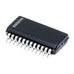
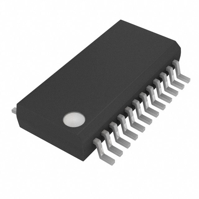
| 供应商器件封装 | 24-SSOP/QSOP |
| 其它名称 | 296-27174-5 |
| 包装 | 管件 |
| 单位重量 | 129.500 mg |
| 商标 | Texas Instruments |
| 安装类型 | 表面贴装 |
| 安装风格 | SMD/SMT |
| 封装 | Tube |
| 封装/外壳 | 24-SSOP(0.154",3.90mm 宽) |
| 封装/箱体 | SSOP-24 |
| 工作电源电压 | 4.5 V to 5.5 V |
| 工厂包装数量 | 50 |
| 接口 | 2 线 |
| 最大工作温度 | + 85 C |
| 最小工作温度 | - 40 C |
| 标准包装 | 50 |
| 电流-电源 | 20mA |
| 电源电流 | 0.5 mA |
| 类型 | 电流发送器 |
| 系列 | XTR108 |
| 输入类型 | 电压 |
| 输出类型 | 电压 |
| 配用 | /product-detail/zh/XTR108EVM/296-21214-ND/1216820 |


- 商务部:美国ITC正式对集成电路等产品启动337调查
- 曝三星4nm工艺存在良率问题 高通将骁龙8 Gen1或转产台积电
- 太阳诱电将投资9.5亿元在常州建新厂生产MLCC 预计2023年完工
- 英特尔发布欧洲新工厂建设计划 深化IDM 2.0 战略
- 台积电先进制程称霸业界 有大客户加持明年业绩稳了
- 达到5530亿美元!SIA预计今年全球半导体销售额将创下新高
- 英特尔拟将自动驾驶子公司Mobileye上市 估值或超500亿美元
- 三星加码芯片和SET,合并消费电子和移动部门,撤换高东真等 CEO
- 三星电子宣布重大人事变动 还合并消费电子和移动部门
- 海关总署:前11个月进口集成电路产品价值2.52万亿元 增长14.8%


PDF Datasheet 数据手册内容提取
XTR108 XTR108 SBOS187C – OCTOBER 2001 – REVISED JULY 2005 4-20mA, TWO-WIRE TRANSMITTER “Smart” Programmable with Signal Conditioning FEATURES DESCRIPTION (cid:1) COMPLETE TRANSMITTER + RTD The XTR108 is a “smart,” programmable, 4-20mA, two-wire LINEARIZATION transmitter designed for temperature and bridge sensors. (cid:1) TWO-WIRE, 4-20mA OUTPUT Zero, span, and linearization errors in the analog signal (cid:1) VOLTAGE OUTPUT (0.5V to 4.5V) path can be calibrated via a standard digital serial interface, eliminating manual trimming. Non-volatile external EEPROM (cid:1) ELIMINATES POTENTIOMETERS AND stores calibration settings. TRIMMING The all-analog signal path contains an input multiplexer, (cid:1) DIGITALLY CALIBRATED autozeroed programmable-gain instrumentation amplifier, dual (cid:1) 5V SUB-REGULATOR OUTPUT programmable current sources, linearization circuit, voltage (cid:1) SERIAL SPI BUS INTERFACE reference, sub-regulator, internal oscillator, control logic, and (cid:1) SSOP-24 PACKAGE an output current amplifier. Programmable level shifting compensates for sensor DC offsets. Selectable up- and down-scale output indicates out-of-range and burn- APPLICATIONS out per NAMUR NE43. Automatic reset is initiated when supply is lost. (cid:1) REMOTE RTD TRANSMITTERS Current sources, steered through the multiplexer, can be (cid:1) PRESSURE BRIDGE TRANSMITTERS used to directly excite RTD temperature sensors, pressure (cid:1) STRAIN GAGE TRANSMITTERS bridges, or other transducers. An uncommitted op amp can (cid:1) SCADA REMOTE DATA ACQUISITION be used to convert current into a voltage. The XTR108 is (cid:1) WEIGHING SYSTEMS specified for –40°C to +85°C. (cid:1) INDUSTRIAL PROCESS CONTROL EEPROM SCLK SDIO CS2 CS1 SPI and Control Circuits et s Excitation Off d n an VPS V/I-0 Linearization ai G V/I-1 4-20mA V/I-2 exer IO V/I-3 pl PGA V/I ulti V/I-4 M V/I-5 RLOAD R1 R2 R3 R4 R5 XTR108 RTD IRet Please be aware that an important notice concerning availability, standard warranty, and use in critical applications of Texas Instruments semiconductor products and disclaimers thereto appears at the end of this data sheet. SPI is a trademark of Motorola, Inc. All other trademarks are the property of their respective owners. PRODUCTION DATA information is current as of publication date. Copyright © 2001-2005, Texas Instruments Incorporated Products conform to specifications per the terms of Texas Instruments standard warranty. Production processing does not necessarily include testing of all parameters. www.ti.com
ABSOLUTE MAXIMUM RATINGS(1) ELECTROSTATIC Loop Supply Voltage, V ............................Dependent on External FET DISCHARGE SENSITIVITY PS XTR Supply Voltage, External V (Referenced to I Pin)............+5.5V S RET Input Voltage to Multiplexer (Referenced to I Pin)................0V to V This integrated circuit can be damaged by ESD. Texas Instru- RET S Output Current Limit................................................................Continuous ments recommends that all integrated circuits be handled with Storage Temperature Range.........................................–55°C to +125°C appropriate precautions. Failure to observe proper handling Junction Temperature....................................................................+165°C and installation procedures can cause damage. Lead Temperature (soldering, 10s)...............................................+300°C ESD damage can range from subtle performance degradation NOTE: (1) Stresses above these ratings may cause permanent damage. to complete device failure. Precision integrated circuits may Exposure to absolute maximum conditions for extended periods may degrade be more susceptible to damage because very small parametric device reliability. changes could cause the device not to meet its published specifications. PACKAGE/ORDERING INFORMATION(1) SPECIFIED PACKAGE TEMPERATURE PACKAGE ORDERING TRANSPORT PRODUCT PACKAGE-LEAD DESIGNATOR RANGE MARKING NUMBER MEDIA, QUANTITY XTR108EA SSOP-24 DBQ –40°C to +85°C XTR108EA XTR108EA Rails " " " " " XTR108EA/2K5 Tape and Reel, 2500 NOTE: (1) For the most current package and ordering information, see the Package Option Addendum at the end of this document, or see the TI website at www.ti.com. ELECTRICAL CHARACTERISTICS ° ° Boldface limits apply over the specified temperature range, T = –40 C to +85 C. A At T = +25°C, V = 24V, and Supertex DN2540 external depletion-mode FET transistor, unless otherwise noted, all voltages measured with respect to I pin. A PS RET XTR108EA PARAMETER CONDITIONS MIN TYP MAX UNITS V TO I TRANSFER FUNCTION I = V (Span) + 4mA IN OUT O IN Output Specified Range 4 20 mA Over-Scale Limit Resolution Digital Select: 21-28.5mA 0.5 mA Fault Over-Scale Level(1) Above Over-Scale Selected +1.0 mA Under-Scale Limit Resolution Digital Select: 2.2-3.6mA 0.2 mA Fault Under-Scale Level(1) Below Under-Scale Selected –0.4 mA Output for Zero Input Zero Error, Unadjusted V = 0V ±50 µA IN vs Temperature ±0.2 ±1.5 µA/°C vs Loop-Supply Voltage, V V = 7.5V to 24V 0.02 µA/V LOOP LOOP vs Common-Mode Voltage V = 0.2V to 3.5V ±1 µA/V CM Adjustment Resolution, Zero Input 1.8 µA/Step Adjustment Range, Zero Input ±4 mA Span(2) Span = I /V O IN Initial, Unadjusted ±1 % Drift (vs Temperature) 40 ppm/°C Span Adjustment Resolution 0.05 % Span Adjustment Range PGA + Output Amplifier(3) R = 6.34kΩ 49.3 3150 mA/V VI Nonlinearity, Ideal Input Full-Scale V = 50mV 0.01 % IN PGA Autozeroing Internal Frequency 6.5 kHz PGA Offset Voltage (RTI)(4) V = 1V ±10 ±50 µV CM vs Temperature ±0.02 µV/°C vs Supply Voltage, V V = 4.5V to 5.5V ±0.5 µV/V S S vs Common-Mode Voltage V = 0.2V to 3.5V 105 dB CM Common-Mode Input Range 0.2 V – 1.5 V S Input Bias Current 50 pA vs Temperature Doubles/10°C pA Input Offset Current 10 pA vs Temperature Doubles/10°C pA XTR108 2 www.ti.com SBOS187C
ELECTRICAL CHARACTERISTICS (Cont.) ° ° Boldface limits apply over the specified temperature range, T = –40 C to +85 C. A At T = +25°C, V = 24V, and Supertex DN2540 external depletion-mode FET transistor, unless otherwise noted, all voltages measured with respect to I pin. A PS RET XTR108EA PARAMETER CONDITIONS MIN TYP MAX UNITS PGA (Cont.) Input Impedance: Differential 30 || 6 GΩ || pF Input Impedance: Common-Mode 50 || 20 GΩ || pF Voltage Noise, 0.1Hz to 10Hz 6 µVp-p PGA Gain Gain Range Steps 6.25, 12.5, 25, 50, 100, 200, 400 6.25 400 V/V Initial Error Gain = 6.25, 12.5, 25, 50 ±0.5 ±2.5 % G = 100, 200 ±0.5 ±3 % G = 400 ±0.8 ±3.5 % vs Temperature ±30 ppm/°C Output Voltage Range(5) R = 6.34kΩ to I 0.2 4.5 V LOAD RET Typical Operating Range for 4-20mA XTR Output 0.5 to 2.5 V Capacitive Drive 200 pF Short-Circuit Current +6/–9 mA ZERO OFFSET DACS Zero-Code Output Level V = 1V, V = 0V CM IN RTO(6) of Current Amplifier R = 6.34kΩ 4.116 mA V/I RTO(6) of PGA 522 mV Coarse DAC, 256 Steps 7 Bits + Sign Adjustment Range Relative to Zero-Code Level RTO(6) of Current Amplifier –3.77 to +3.77 mA RTO(6) of PGA –470 to +470 mV Step Size RTO(6) of Current Amplifier 0.029 mA RTO(6) of PGA 3.7 mV Linearity ±0.5 LSB Fine DAC, 256 Steps Relative to Zero-Code Level 7 Bits + Sign Adjustment Range RTO(6) of Current Amplifier –236 to +236 µA RTO(6) of PGA –29.4 to +29.4 mV Step Size RTO(6) of Current Amplifier 0.0018 mA RTO(6) of PGA 0.23 mV Linearity ±1 LSB Noise, RTO(6) f = 0.1Hz to 10Hz 1.1 µAp-p CURRENT AMPLIFIER Current Gain 49 50 51 A/A Current Gain Drift 10 ppm/°C CURRENT SOURCES, I AND I REF1 REF2 Zero-Code Output Level, Each R = 12.1kΩ 480 493 510 µA SET Coarse DAC, 256 Steps 7 Bits + Sign Adjustment Range(7) –195 to +195 µA Step Size 1.54 µA Fine DAC, 256 Steps 7 Bits + Sign Adjustment Range(7) –12.2 to +12.2 µA Step Size 96 nA Linearity Coarse ±0.2 LSB Fine ±0.5 LSB vs Temperature ±35 ppm/°C Matching ±0.2 % vs Temperature ±10 ppm/°C Compliance Voltage, Positive(5) V – 2 V – 1.5 V S S Output Impedance 100 MΩ Current Noise f = 0.1Hz to 10Hz 0.015 µAp-p LINEARIZATION DAC Linearization Range, 256 Steps 8 Bits Max Linearization Coefficient ∆I /∆V , R = 15.8kΩ 0.99 µA/mV REF IN LIN Step Size 3.9 nA/mV SUB-REGULATOR, V Supply Voltage for XTR S Voltage 4.8 5.1 5.4 V vs Temperature ±50 ppm/°C vs Loop-Supply Voltage V = 7.5V to 24V ±0.03 mV/V LOOP XTR108 3 SBOS187C www.ti.com
ELECTRICAL CHARACTERISTICS (Cont.) ° ° Boldface limits apply over the specified temperature range, T = –40 C to +85 C. A At T = +25°C, V = 24V, and Supertex DN2540 external depletion-mode FET transistor, unless otherwise noted, all voltages measured with respect to I pin. A PS RET XTR108EA PARAMETER CONDITIONS MIN TYP MAX UNITS OVER- AND UNDER-SCALE LIMITING Over-Scale DAC: 16 Steps 4 Bits Adjustment Range RTO(6) of Current Amplifier R = 6.34kΩ 20.7 to 28.1 mA VI RTO(6) of PGA 2.625 to 3.563 V Step Size RTO(6) of Current Amplifier 0.49 mA RTO(6) of PGA 62.5 mV Accuracy ±10 % Under-Scale DAC: 8 Steps 3 Bits Adjustment Range RTO(6) of Current Amplifier R = 6.34kΩ 2.17 to 3.55 mA VI RTO(6) of PGA 275 to 450 mV Step Size RTO(6) of Current Amplifier 0.195 mA RTO(6) of PGA 25 mV Accuracy ±5 % VOLTAGE REFERENCE, V REF Internal Bandgap 1.193 V vs Temperature ±5 ±50 ppm/°C UNCOMMITTED OP AMP Input Offset Voltage V = 2V ±2 mV CM vs Temperature ±3 µV/°C vs Common-Mode Voltage 90 dB Open-Loop Gain 110 dB Common-Mode Input Range 0 to 3.5 V Output Voltage Range R = 10kΩ to V /2 0.2 V – 0.2 V L S S DIGITAL INPUT/OUTPUT Logic Family CMOS Logic Levels V 0 0.8 V IL V 3.5 V V IH S V I = 300µA 0.4 V OL OL V I = –300µA V – 1 V OH OH S Input Current I (CS1) 3.5 < V < V –200 –120 10 µA IH IN S I (CS1) 0 < V < 0.8 –20 –6 10 µA IL IN I , I (SCLK, DIO) 0 < V < V –20 –6 10 µA IH IL IN S INTERNAL OSCILLATOR Frequency, f 210 kHz OSC TEMPERATURE RANGE Specification –40 +85 °C Operating –55 +125 °C θ , Junction to Ambient 100 °C/W JA LOOP SUPPLY Voltage Range with Supertex DN2540 7.5 V Quiescent Current R Open, L Reg = 0, No Sensor Current(8)(9) 0.5 mA SET IN NOTES: (1) Over-scale and under-scale complies with NAMUR NE43 recommendation. (2) Span adjustment is determined by PGA gain and sensor excitation. (3) Span can be digitally adjusted in three ways: PGA gain, current reference Coarse, and current reference Fine. (4) RTI = Referred to Input. (5) Current source output voltage measured with respect to I . (6) RTO = Referred to Output. (7) Excitation DAC range sufficient to adjust span fully RET between PGA gain steps. (8) Output current into external circuitry is limited by an external MOS power FET. (9) Measured with over- and under-scale limits disabled. XTR108 4 www.ti.com SBOS187C
PIN CONFIGURATION Top View SSOP V/I-0 1 24 OPA +IN V/I-1 2 23 OPA –IN V/I-2 3 22 OPA OUT V/I-3 4 21 REF OUT V/I-4 5 20 REF IN V/I-5 6 19 R SET XTR108 C 7 18 CS1 FILTER R 8 17 SCLK LIN V 9 16 SDIO O I 10 15 CS2 IN I 11 14 V O GATE I 12 13 V RET S PIN ASSIGNMENTS PIN NAME FUNCTION V/I-0 MUX Input Channel 0 and/or I Out MUX Input to PGA and/or I to Sensor REF REF V/I-1 MUX Input Channel 1 and/or I Out MUX Input to PGA and/or I to Sensor REF REF V/I-2 MUX Input Channel 2 and/or I Out MUX Input to PGA and/or I to Sensor REF REF V/I-3 MUX Input Channel 3 and/or I Out MUX Input to PGA and/or I to Sensor REF REF V/I-4 MUX Input Channel 4 and/or I Out MUX Input to PGA and/or I to Sensor REF REF V/I-5 MUX Input Channel 5 and/or I Out MUX Input to PGA and/or I to Sensor REF REF C Filter Capacitor Filter to Reduce Chopper Noise in Autozeroing PGA FILTER R Linearization Linearization Range Adjustment Resistor LIN V PGA Output PGA Amplified Output of Differential Sensor Input O I Current Input Input to Output Current Amplifier IN I Output Current 4-20mA Current for Output Loop O I Return Current Return for All External Circuitry Current RET V Voltage Regulator Supply Voltage for XTR and External Circuitry, If Used S V Gate Voltage Gate Voltage for External MOSFET Transistor GATE CS2 Chip Select 2 Select for XTR Serial Port to External EEPROM (Output from XTR Only) SDIO Serial Data Input/Output Serial Data Input or Output SCLK Serial Clock Serial Clock CS1 Chip Select 1 Select for External µC Serial Port (Input to XTR Only) R Resistor for Reference Sets Current Reference SET REF Voltage Reference Input Voltage Reference Input to XTR IN REF Voltage Reference Output Voltage Reference Output from Internal Bandgap OUT OPA OUT Uncommitted Op Amp Output Uncommitted Op Amp Output OPA –IN Uncommitted Op Amp Negative Input Uncommitted Op Amp Negative Input OPA +IN Uncommitted Op Amp Positive Input Uncommitted Op Amp Positive Input XTR108 5 SBOS187C www.ti.com
TYPICAL CHARACTERISTICS At T = +25°C, V+ = 24V, unless otherwise noted. R = 6.34kΩ. A VI TRANSCONDUCTANCE vs FREQUENCY COMMON-MODE REJECTION vs FREQUENCY 70 90 60 G = 400 mAnductance (20log )V 5432100000 G = 50 G = 200 mAection (20log )V 8765400000 G = 6.25 G = 100 sco 0 Rej 30 an –10 G = 6.25 Tr –20 20 G = 400 –30 10 100 1k 10k 100k200k 10 100 1k 10k 100k Frequency (Hz) Frequency (Hz) I V REJECTION RATIO vs FREQUENCY I V REJECTION RATIO vs FREQUENCY ZERO LOOP REF LOOP 100 120 90 110 80 e e uctancmA/V)) 70 uctancmA/V)) 100 ndg( 60 ndg( 90 oo oo nsc20 l 50 nsc20 l a– a– 80 Tr( Tr( 40 70 30 20 60 10 100 1k 10k 10 100 1k 10k Frequency (Hz) Frequency (Hz) I vs TEMPERATURE I DRIFT AVERAGE REF OUT 492 20% 18% 16% 490 nits 14% µI (A)REF ercent of U 11820%%% 488 P 6% 4% 2% 486 0% –75 –50 –25 0 25 50 75 100 125 0 0 0 0 0 0 0 0 0 0 0 9 7 5 3 1 1 3 5 7 9 0 Temperature (°C) –0. –0. –0. –0. –0. 0. 0. 0. 0. 0. 1. I Drift (µA/°C) OUT XTR108 6 www.ti.com SBOS187C
TYPICAL CHARACTERISTICS (Cont.) At T = +25°C, V+ = 24V, unless otherwise noted. R = 6.34kΩ. A VI LARGE INPUT STEP RESPONSE LARGE INPUT STEP RESPONSE N N VI VI 20mA 20mA T U O I UT O I 4mA 4mA PGA Gain = 6.25 C = 0 PGA Gain = 6.25 C = 0.01µF FILT FILT 250µs/div 500µs/div SMALL INPUT STEP RESPONSE SMALL INPUT STEP RESPONSE VIN VIN 20mA 20mA T U UT IO O I 4mA 4mA PGA Gain = 200 C = 0 PGA Gain = 200 C = 0.01µF FILT FILT 250µs/div 500µs/div I NOISE POWER I CURRENT NOISE POWER REF ZERO 10 100 z) z) H H √ √ A/ A/ n n y ( y ( sit 1.0 sit 10 n n e e D D e e s s oi oi N N 0.1 1 1 10 100 1k 10k 1 10 100 1k 10k Frequency (Hz) Frequency (Hz) XTR108 7 SBOS187C www.ti.com
TYPICAL CHARACTERISTICS (Cont.) At T = +25°C, V+ = 24V, unless otherwise noted. R = 6.34kΩ. A VI INPUT NOISE POWER DENSITY PGA PEAK-TO-PEAK NOISE (RTI) 1000 BW: 0.1Hz to 10Hz z) H √ V sity (n 100 µV/div n 5 e 2 e D 1. s oi N C = 0.01 FILT 10 1 10 100 1k 10k 5s/div Frequency (Hz) OVERVIEW The XTR108 is a 4-20mA current-loop transmitter that allows the user to digitally adjust the gain, offset, and EE PROM linearity correction of the analog output to calibrate the SDIO sensor. The digital data for adjustment are stored in an S2 SCLK Isolation Calibration external EEPROM device. C CS1 Couplers System The analog signal path is composed of a compound multi- plexer (MUX), programmable gain instrumentation amplifier Calib (PGA), and an output current amplifier. Analog support func- GND tions include digitally controlled current sources for sensor excitation, PGA offset control, linearization, voltage refer- XTR108 ence, and voltage regulator. IO The digital interface communicates with external devices for calibration and to store the resultant data in an SPI compat- IRET RV PS ible EEPROM. A complete system is shown in Figure 1. The XTR108 serial interface is SPI compatible and only requires TX RX four connections to the calibration controller: a serial clock GND GND (SCLK), a serial data line (SDIO), a chip select line (CS1), and a ground sense line. All logic signals to the XTR108 must be referenced to the potential of the ground sense line FIGURE 1. Complete System Level Configuration with (I pin on the XTR108). RET Three Unique Ground Voltage Levels. Within this entire system there may exist three different “GND” voltage levels. In addition, the voltage difference The XTR108 also needs to communicate with the external between the I and I potential will depend on the output RET O EEPROM device independently from the calibration control- current level. It is not certain that the “GND” potential of the ler to retrieve the calibration constants during normal opera- calibration system will be at the same potential of either the tion. The XTR108 provides a second chip select function I or I potential, and therefore the isolation couplers are RET O (CS2) for the EEPROM device to facilitate this communica- shown in Figure 1. All voltages specified for the XTR108 tion. are with reference to the I pin. RET XTR108 8 www.ti.com SBOS187C
THEORY OF OPERATION If over-scale and under-scale limiting is disabled, the PGA can be used with rail-to-rail voltage output, for example, in REFERENCE applications that require a 0.5V to 4.5V voltage scale. The XTR108 has an on-board precision bandgap voltage The PGA uses advanced auto-zero circuit techniques to achieve reference with output at pin 21 (REF ). The value of the high DC precision, and reduce mismatches and errors within OUT reference is factory-trimmed to 1.193V, with a typical tem- the chip such as input offset, offset temperature drift, and low- perature drift of 5ppm/°C. Pins 21 (REF ) and 20 (REF ) frequency noise (see the input noise typical characteristic). OUT IN must be connected together to use the internal reference. The basic clock frequency of the auto-zero loop is about External circuitry, such as a voltage excited sensor or an 6.5kHz. Due to the switching nature of the auto-zero circuit, Analog-to-Digital Converter (ADC), can be connected to the the output of the PGA can have a noticeable clock feed- REF pin. The unbuffered REF is capable of sourcing through ripple in higher gains. This noise can be reduced by OUT OUT current but not sinking. the addition of a 0.01µF capacitor between pin 7 (C ) FILTER If the application necessitates, an external reference can be and the local ground, pin 12 (IRET). This creates a one-pole connected to the XTR108 REF pin, as long as the reference low-pass filter with –3dB frequency at about 1.5kHz. If IN does not exceed 1.4V. The REFIN pin has a high input wider bandwidth or faster settling time is needed, the CFILTER impedance with the input current not exceeding a few can be reduced or eliminated at the expense of higher glitch nanoamps. amplitude at the output. Please refer to the typical step response traces for settling time comparisons. INPUT MULTIPLEXER ZERO DACS The XTR108 input multiplexer is a full 6 by (2+2) cross- point switch. The current references and PGA inputs can be Two output-referred, 8-bit Digital-to-Analog Converters independently connected to any of the six external pins, (DACs) (coarse and fine with a pedestal) set the zero level of including simultaneous connections to the same pin. This the PGA output. They allow setting a desired zero-scale allows a great flexibility in the sensor excitation and input output level and compensate the initial offset at the PGA input configuration. The input pins must not be driven below the due to the sensor and resistor mismatches, sensor non-ideali- I potential or above V . ties, etc. Both coarse and fine DACs are bidirectional and RET S allow the output level to be set above or below a preset See Figure 2 for an RTD sensor connected to pin V 0 with IN pedestal. both I supplied and PGA V sensed at that pin. The REF IN+ other five input pins are used for a bank of RZ resistors that Output signals of the DACs, IZ COARSE and IZ FINE, are can be selected during the calibration process for a particular summed with the pedestal, IZ PROGRAM. Each of the DACs measurement range. has 8-bit resolution (256 steps) with 4-bit overlap between the coarse and fine DACs. This means that one LSB of the coarse DAC is equal to 16 fine LSBs, and the full-scale PROGRAMMABLE GAIN range of the fine DAC is equal to 16 coarse LSBs. This INSTRUMENTATION AMPLIFIER effectively produces 12-bit adjustment resolution. The programmable gain instrumentation amplifier has seven This overlap allows the user to set pre-calculated values voltage-gain settings in binary steps from 6.25V/V to 400V/V. before the calibration, using the coarse DAC only and adjust The input common-mode range of the PGA is 0.2V to 3.5V the zero output level with the fine DAC during the calibra- above the I potential. RET tion process see Table II for the equations for calculating the Normally, in the application for 4-20mA transmitters, the value of the output when zero differential voltage is applied PGA output voltage range should be set to VZERO = 0.5V and at the PGA input. For the adjustment range, LSB sizes, and VFS = 2.5V. Connecting a resistor (RVI = 6.34kΩ) between linearity values of the Zero DACs, please refer to the pin 9 (VO) and pin 10 (IIN) converts this voltage to the signal electrical characteristics table. for the output amplifier that produces a 4-20mA scale Note that a DAC can be set to a value that produces an current output. In this mode, the PGA voltage gain converts output below the under-scale level. In this case, the under- to an overall transconductance in the range of 50mA/V to scale limit will prevent the output from getting to the desired 3200mA/V (approximately). Table I shows the gain to value. The value of the minimum scale should not be set so transconductance relationship. low that the PGA voltage output, V , goes below its speci- O fied range of 0.2V from I . RET VOLTAGE GAIN 6.25 12.5 25 50 100 200 400 V/V ADJUSTABLE OVER-SCALE AND OUTPUT TRANSCONDUCTANCE 49 99 197 394 789 1577 3155 UNDER-SCALE LIMITING CIRCUIT mA/V The XTR108 incorporates circuitry to set adjustable limits at FULL-SCALE DIFFERENTIAL V 320 160 80 40 20 10 5 IN the output in cases when the sensor signal goes above or mV below its range. There are 16 levels for over-scale limit TABLE I. PGA Gain, Corresponding Loop Transductance adjustment (4-bit DAC) and 8 levels for the under-scale (3-bit and Input Full-Scale Differential Voltage. DAC). XTR108 9 SBOS187C www.ti.com
y LoopSuppl RLOAD + – P O O CL A m 4-20 CREG E AT G REFIN REFOUT VGate VS C IO RET I 8 0 1 R e T VoltageReferenc X b-RegulatorDriver OutputCurrentAmplifier Ω1 u 5 S Ω 5k 2. SC IIN O Ω SCLK VOUT RVI6.34k SDIO PI andol Circuits RSET Ω12.1k CS1CS2 SContr earizationCircuit RLIN Ω15.8k oC n erA Li ZD F µ 1 A +IN IREFDAC ILINDAC PGA CFILT 0.0 P O N –I A P Σ O 2 rexelpitluM 1 0 1 2 3 4 5 UT V/I- V/I- V/I- V/I- V/I- V/I- RZ5 A O RZ4 P O RZ3 RZ2 RZ1 M C R D T R FIGURE 2. XTR108 Internal Block Diagram. XTR108 10 www.ti.com SBOS187C
VOLTAGE REFERRED TO V PIN O WITH RESPECT TO I CURRENT REFERRED TO I PIN RET OUT OVERALL V = V + V + V I = I + I + I ZERO Z PROGRAM Z COARSE Z FINE ZERO Z PROGRAM Z COARSE Z FINE PROGRAM VZPROGRAM= 3.5V8REF IZPROGRAM=1785RVVRIEF COARSE DAC VZCOARSE = V8R0EF •N413 IZCOARSE = 58VRRVEIF •N413 FINE DAC VZFINE = V8R0EF •N6142 IZFINE = 58VRRVEIF •N6142 NOTE: N and N are assigned decimal values of registers 13 and 12, respectively. 13 12 TABLE II. Equations for Calculating Zero Output. The circuit is designed for compliance with NAMUR NE43 matched internal resistors determines a current gain of this recommendation for sensor interfaces. The limit levels are block. Note that the I pin is always biased below the OUT listed in Tables VII and VIII. Because of the large step sizes, substrate potential. units that use this feature should be checked if the value is critical. The under-scale limit circuit will override the Zero EXCITATION CURRENT DACS AND R RESISTOR SET DAC level if it is set lower and there is not enough sensor Two matched adjustable reference current sources are avail- offset at the PGA input. able for sensor excitation. The defining equations are given It may be necessary to disable limiting if the XTR108 is used in Table III. Both current sources are controlled simulta- in applications other than a 4-20mA transmitter, where the neously by the coarse and fine DACs with a pedestal. PGA output is between 0.5V and 4.5V. The external resistor R is used to convert the REF voltage SET into the reference current for the sensor excitation DACs. SENSOR FAULT DETECTION CIRCUIT The total current output of the DACs is split, producing two To detect sensor burnout and/or short, a set of four compara- references: I and I . Both of the current references REF1 REF2 tors is connected to the inputs of the PGA. If any of the match very closely over the full adjustment range without inputs are taken outside of the PGA’s common-mode range, mismatched differential steps. Both current reference out- the corresponding comparator sets a sensor fault flag that puts must be within the compliance range, i.e.: one reference causes the PGA output to go either to the upper or lower cannot be floated since it will change the value of the other error limit. The state of the fault condition can be read in the current source. digital form from register 3. The direction of the analog The recommended value of R is 12.1kΩ for use with SET output is set according to the “Alarm Configuration Regis- 100Ω RTD sensors. This generates I = 492µA currents REF1, 2 ter” (see Table X). The level of the output is produced as when both coarse and fine DACs are set to zero. The value follows: if the over-scale/under-scale limiting is enabled, the of the R resistor can be increased if lower reference SET error levels are: over-scale limit +2LSBs of the over-scale currents are required, i.e.: for 1000Ω RTD or a bridge DAC, about 1mA referred to IOUT or 0.125V referred to VO, sensor. of under-scale limit –2LSBs of the under-scale DAC, about 0.4mA referred to I or 0.05V referred to V . If the over- OUT O REFERENCE CURRENT scale/under-scale limiting is disabled, the PGA output volt- age will go to within 150mV of either positive or negative OVERALL IREF1, 2 = IREF PROGRAM + IREF COARSE + IREF FINE supply (VS or IRET), depending on the alarm configuration PROGRAM IREFPROGRAM= 5RVREF bit corresponding to the error condition. SET V N COARSE DAC IREFCOARSE =RREF • 6141 SET OUTPUT CURRENT AMPLIFIER + R RESISTOR VI V N To produce the 4-20mA output, the XTR108 uses a current FINE DAC IREFFINE =RREF •101204 SET amplifier with a fixed gain of 50A/A. The voltage from the NOTE: N and N are the decimal values of registers 11 and 10, PGA is converted to current by the external resistor, RVI. Pin respective11ly. 10 I , the common potential of the circuit (substrate and local RET TABLE III. Equations for Calculating the Values of Each ground), is connected to the output and inverting input of the Reference Current. amplifier. This allows collecting all external and internal supply currents, sensor return current, and leakage currents Similar to the Zero DACs, the outputs of the fine and coarse from the different parts of the system and accounting for DAC are summed together with the pedestal I . them in the output current. The current from R flows into REF PROGRAM VI Each of the excitation DACs has 8-bit resolution (256 steps) the pin I that is connected to the noninverting input and IN with 4-bit overlap between the coarse and the fine. This therefore, is at ground potential as well. The ratio of two XTR108 11 SBOS187C www.ti.com
means that one LSB of the coarse DAC is equal to 16 fine n-channel depletion-mode MOS transistor and three capaci- LSBs, and the full-scale range of the fine DAC is equal to 16 tors, see Figure 2. coarse LSBs. This effectively produces 12-bit adjustment A number of third-party suppliers make n-channel deple- resolution. This allows the user to set pre-calculated values tion-mode MOSFETs. A list of devices tested by Texas before the calibration, using the coarse DAC only and adjust Instruments, Inc. is shown in Table IV with the capacitor the reference current output level with the fine DAC during values recommended for those devices. the calibration process. MANUFACTURER MOSFET MODEL C VALUE LINEARIZATION CIRCUIT AND R RESISTOR GATE LIN Supertex DN2535, DN2540 220pF The XTR108 incorporates circuitry for correcting a second- DN3535, DN3525 1000pF order sensor nonlinearity. A current proportional to the Siliconix ND2012, ND2020 220pF voltage at the input of the PGA is added to the sensor Infineon BSP149 1000pF excitation. The R resistor is used to convert this voltage LIN TABLE IV. Recommended Gate Capacitor Values For Se- into current. By appropriately scaling this current using the lected MOSFETs. linearization DAC, parabolic sensor nonlinearity can be improved by up to a 40:1 ratio, as shown in Figure 3. The The capacitors C (0.01µF), C (2.2µF), and C linearization coefficient (ratio of the reference current change LOOP REG GATE to the input voltage) is expressed in µA/mV as follows: are required for the regulator loop stability and supply bypass. They should be placed in close proximity to the G = ∆IREF • N14 XTR108 on the PCB. An additional 1µF capacitor may be LIN V 16•R used to bypass the supply of an EEPROM chip. IN LIN If a MOSFET other than those listed in Table IV is used, the where N is the decimal value from register 14. 14 value of C should be adjusted such that there is no The recommended value of the resistor is 15.8kΩ, for use GATE overshoot of V during power-up and supply glitches. Any with 100Ω RTD sensors. This value produces a full-scale S V overshoot above 7.5V may damage the XTR108 or linearization coefficient of about 1mA/V. Please see the S deteriorate its performance. section below on using the XTR108 with an RTD tempera- ture sensor. If the sensor excitation is scaled down by LOOP VOLTAGE increasing the value of R , the value of R should be SET LIN scaled proportionally. The XTR108 transmitter minimum loop voltage can some- what be effected by the choice of the external MOSFET. The devices are tested to 7.5V compliance with Supertex DN2540; choosing other MOSFETs can change this value slightly. The maximum loop voltage is limited by the power dissipa- 5 tion on the MOSFET as well as its breakdown voltage. Possible ambient temperatures and the power dissipation 4 should be taken into account when selecting the MOSFET package. The external MOSFET can dissipate a consider- %) 3 y ( Uncorrected able amount of power when running at high loop supply. For earit 2 RTD Nonlinearity example, if VLOOP = 24V and IOUT = 20mA, the DC power nlin dissipated by the MOSFET is: No 1 Corrected P = I (V – V ) = 380mΩ Nonlinearity MOSFET OUT LOOP S 0 For a SOT-89 package soldered on an FR5 board, this will cause a 30°C rise in the temperature. The power dissipation –1 gets significantly higher when the circuit is driven into an –200°C +850°C over-scale condition. Therefore, special attention should be Process Temperature (°C) paid to removing the heat from the MOSFET, especially with small-footprint packages such as SOT-89 and TO-92. Please follow manufacturer’s recommendations about the FIGURE 3. Pt100 Nonlinearity Correction Using the XTR108. package thermal characteristics and board mounting. SUB-REGULATOR WITH EXTERNAL MOSFET UNCOMMITTED OP AMP The XTR108 is manufactured using a low-voltage CMOS For added flexibility in various applications, the XTR108 process with maximum supply voltage limited to 5.5V. For has an on-chip uncommitted operational amplifier. The op applications in a 4-20mA current loop, a special sub-regulator amp has rail-to-rail output range. The input range extends to circuit is incorporated in the device that requires an external I potential. RET XTR108 12 www.ti.com SBOS187C
The uncommitted amplifier can be used for a variety of CONTROL REGISTERS purposes, such as voltage sensor excitation, buffering the REF pin, four-wire RTD connection, or sensing the Table V shows the registers that control the analog functions OUT bridge voltage for temperature compensation. of the XTR108. POWER-GOOD/POWER-ON RESET DESCRIPTION OF CONTROL REGISTERS In case of a supply brownout condition or short interruption, Address = 0: Control Register 1 the XTR108 power-good detection circuit will initiate a chip If the RST bit is set to ‘1’ in a write operation, all the reset that will cause all registers to be reset to 0’s and a cycle registers in the XTR108 will be returned to their power-on of EEPROM read to begin. The circuit generates a reset if reset condition. The RST bit will always read as a ‘0’. CSE, V droops below 1.5V and then recovers up to the normal the checksum error bit, is read only and will be set to ‘1’ if S level. a checksum error has been detected. This bit is cleared by a reset operation or by detection of a valid checksum. The USING THE XTR108 IN VOLTAGE OUTPUT MODE remaining bits are reserved and must be set to ‘0’. Address = 3: Fault Status Register The XTR108 can be used not only in 4-20mA current loops, but also as a low-power, single-supply, "smart" sensor- This register is a read-only register. If the input voltage to conditioning chip with voltage output. In this mode, the PGA exceeds the linear range of operation, the XTR108 the I pin must be connected below ground will indicate this error condition (typically caused by a RET (–200mV < I < –25mV). This negative voltage is sensor fault) by setting the under-scale or over-scale error RET required to overcome the input offset voltage of the output level depending on the state of the Alarm Configuration current amplifier and prevent it from turning on and drawing Register (Address = 7). Information on the nature of the fault excessive current. An application circuit that generates this may be read in digital form from this register, as shown in negative voltage using the XTR108 clock output and a Table VI. The remaining bits will be set to ‘0’. simple charge pump is shown in the application section. The sub-regulator with an external MOSFET may or may not BIT FAULT MODE be used. If the circuit is powered externally, the supply F0 Negative Input Exceeds Positive Limit. voltage must be in the range of 5V ±0.5V. F1 Negative Input Exceeds Negative Limit. F2 Positive Input Exceeds Positive Limit. F3 Positive Input Exceeds Negative Limit. TABLE VI. Register 3, Fault Status Register. Instruction D7 D6 D5 D4 D3 D2 D1 D0 Read/Write R/W 0 0 0 A3 A2 A1 A0 Read/Write Operation EEPROM Mode 0 1 1 1 1 1 1 1 Assert CS2 Ignore Serial Data/A Data Bit D7 D6 D5 D4 D3 D2 D1 D0 0 RST CSE 0 0 0 0 0 0 Read/Write Control Register 1 1 0 0 0 0 0 0 0 0 Reserved 2 0 0 0 0 0 0 0 0 Reserved 3 0 0 0 0 F3 F2 F1 F0 Read Only Fault Status Register 4 0 0 0 0 0 0 0 RBD Read/Write Control Register 2 5 FD US2 US1 US0 OS3 OS2 OS1 OS0 Read/Write Over/Under-Scale Register 6 0 0 0 0 0 G2 G1 G0 Read/Write PGA Gain 7 AC7 AC6 AC5 AC4 AC3 AC2 AC1 AC0 Read/Write Alarm Config. Register 8 0 VP2 VP1 VP0 0 VN2 VN1 VN0 Read/Write PGA Input Config. Register 9 0 IB2 IB1 IB0 0 IA2 IA1 IA0 Read/Write I Output Config. Register REF 10 FG7 FG6 FG5 FG4 FG3 FG2 FG1 FG0 Read/Write Fine I Adjust Register REF 11 CG7 CG6 CG5 CG4 CG3 CG2 CG1 CG0 Read/Write Coarse I Adjust Register REF 12 FZ7 FZ6 FZ5 FZ4 FZ3 FZ2 FZ1 FZ0 Read/Write Fine Zero Adjust Register 13 CZ7 CZ6 CZ5 CZ4 CZ3 CZ2 CZ1 CZ0 Read/Write Coarse Zero Adjust Register 14 L7 L6 L5 L4 L3 L2 L1 L0 Read/Write Linearization Adjust Register 15 S7 S6 S5 S4 S3 S2 S1 S0 Read/Write Checksum Register TABLE V. Analog Control Registers. XTR108 13 SBOS187C www.ti.com
Address = 4: Control Register 2 I UNDER-SCALE O If the RBD bit is set to ‘1’, the automatic read-back from the VO UNDER-SCALE THRESHOLD US2 US1 US0 THRESHOLD R = 6.34kΩ EEPROM will be disabled after a valid checksum byte is VI received in Register 15. This bit is read from the EEPROM 0 0 0 450mV 3.55mA 0 0 1 425mV 3.35mA during a read-back by the XTR108 and allows the user to 0 1 0 400mV 3.15mA program the XTR108 to read the EEPROM data once 0 1 1 375mV 2.96mA (instead of continuously), and then disables the automatic 1 0 0 350mV 2.76mA 1 0 1 325mV 2.56mA read-back function. The XTR108 will continuously read the 1 1 0 300mV 2.37mA EEPROM if RBD is set to ‘0’. The remaining bits in this 1 1 1 275mV 2.17mA register must be set to ‘0’. TABLE VIII. Register 5, Under-Scale Threshold. Address = 5: Over- and Under-Scale Register This register sets the magnitude of the over-scale current SIGNAL PATH limit and the magnitude of the under-scale current limit. The PGA TRANSCONDUCTANCE threshold level, as shown in Table VII and VIII, is the G2 G1 G0 VOLTAGE GAIN R = 6.34kΩ VI normal analog (no error condition) output limit. If an input 0 0 0 6.25V/V 49mA/V voltage to the PGA exceeds the linear operation range, the 0 0 1 12.5V/V 99mA/V 0 1 0 25V/V 197mA/V output will be programmed to either the over-scale error 0 1 1 50V/V 394mA/V level or the under-scale error level. The over-scale error 1 0 0 100V/V 789mA/V level is 10mA greater than the over-scale threshold level. 1 0 1 200V/V 1577mA/V 1 1 0 400V/V 3155mA/V The under-scale error level is 0.4mA less than the under- 1 1 1 Reserved scale threshold level. The FD bit will disable the over-scale TABLE IX. Register 6, PGA Gains. and under-scale limiting function as well as the PGA fault indication error levels. Address = 6: PGA Gain Register BIT AC AC AC AC AC AC AC AC This register sets the gain of the programmable-gain ampli- # 7 6 5 4 3 2 1 0 V h l l h n n l h fier. The unused bits must always be set to ‘0’. The gain step INN V l h l h l h n n INP to register content is given in Table IX. NOTES: ‘h’ = input exceeds positive common-mode range, ‘l’ = input exceeds Address = 7: Alarm Configuration Register negative common-mode range, and ‘n’ = input pin is within the CM range. This register configures whether the XTR108 will go over- TABLE X. Register 7, Alarm Configuration Register. scale or under-scale for various detected fault conditions at the input of the PGA. Table X defines each of the bits. Address = 8: PGA Input Configuration Register If a bit corresponding to the particular error is set to ‘1’, the This register connects the inputs of the PGA to the various output will go over-scale when it occurs and if a bit corre- multiplexed input pins. Tables XI and XII show the relation- sponding to the particular error is set to ‘0’, the output will ship between register, contents, and PGA inputs. go under-scale. VP2 VP1 VP0 PGA POSITIVE INPUT I OVER-SCALE O 0 0 0 PGA V Connected to V/I-0 V OVER-SCALE THRESHOLD IN+ OS3 OS2 OS1 OS0 OTHRESHOLD R = 6.34kΩ 0 0 1 PGA VIN+ Connected to V/I-1 VI 0 1 0 PGA V Connected to V/I-2 IN+ 0 0 0 0 2.625V 20.7mA 0 1 1 PGA V Connected to V/I-3 IN+ 0 0 0 1 2.6875V 21.2mA 1 0 0 PGA V Connected to V/I-4 IN+ 0 0 1 0 2.75V 21.7mA 1 0 1 PGA V Connected to V/I-5 IN+ 0 0 1 1 2.8125V 22.2mA 1 1 0 Reserved 0 1 0 0 2.875V 22.7mA 1 1 1 Reserved 0 1 0 1 2.9375V 23.2mA 0 1 1 0 3.0V 23.7mA TABLE XI. Register 8, PGA Positive Input Selection. 0 1 1 1 3.0625V 24.2mA 1 0 0 0 3.125V 24.6mA 1 0 0 1 3.1875V 25.1mA VN2 VN1 VN0 PGA NEGATIVE INPUT 1 0 1 0 3.25V 25.6mA 1 0 1 1 3.3125V 26.1mA 0 0 0 PGA VIN– Connected to V/I-0 1 1 0 0 3.375V 26.6mA 0 0 1 PGA VIN– Connected to V/I-1 1 1 0 1 3.4375V 27.1mA 0 1 0 PGA VIN– Connected to V/I-2 1 1 1 0 3.5V 27.6mA 0 1 1 PGA VIN– Connected to V/I-3 1 1 1 1 3.5625V 28.1mA 1 0 0 PGA VIN– Connected to V/I-4 1 0 1 PGA V Connected to V/I-5 IN– TABLE VII. Register 5, Over-Scale Threshold. 1 1 0 Reserved 1 1 1 Reserved TABLE XII. Register 8, PGA Negative Input Selection. XTR108 14 www.ti.com SBOS187C
Address = 9: I Output Configuration Register SERIAL INTERFACE REF This register connects the reference currents to the various PROTOCOL multiplexed input pins. I connection codes are given in REF Table XIII. The XTR108 has an SPI-compatible serial interface. The data is transmitted MSB first in 8-bit bytes. The first byte is Address = 10: Fine I Adjust Register REF an instruction byte in which the first bit is a read/write flag This register sets the code to the 8-bit Fine DAC that adjusts (‘0’ = write, ‘1’ = read), the lowest four bits are the register the magnitude of both reference currents. The DAC output address and the remaining three bits are set to zero. The value has a bipolar range (for each reference current) and second, and all successive bytes, are data. During a write can be calculated using the equations in Table III. operation, the successive data bytes are written to successive registers within the XTR108. The address is automatically incremented at the completion of each byte. The SDIO line IA2 IA1 IA0 I CONNECTION REF is always an input during a write operation. During a read 0 0 0 I 1 Connected to V/I-0 REF operation, the SDIO line becomes an output during the 0 0 1 I 1 Connected to V/I-1 REF 0 1 0 I 1 Connected to V/I-2 second and successive bytes. As in the case of a write REF 0 1 1 IREF1 Connected to V/I-3 operation, the address is automatically incremented at the 1 0 0 I 1 Connected to V/I-4 REF completion of each byte. Each communication transaction is 1 0 1 I 1 Connected to V/I-5 REF 1 1 0 Reserved terminated when CS1 is de-asserted. The CS2 line remains 1 1 1 Reserved de-asserted during read and write operations. IB2 IB1 IB0 IREF CONNECTION The calibration controller also needs to be able to read from 0 0 0 I 2 Connected to V/I-0 and write to the external EEPROM device. This is accom- REF 0 0 1 IREF2 Connected to V/I-1 plished by sending a special instruction code (0x7F) to the 0 1 0 I 2 Connected to V/I-2 REF XTR108. At the completion of this instruction byte, the 0 1 1 I 2 Connected to V/I-3 REF 1 0 0 I 2 Connected to V/I-4 XTR108 will assert the CS2 line to select the EEPROM REF 1 0 1 IREF2 Connected to V/I-5 device and ignore all data on the SDIO line until CS1 is de- 1 1 0 Reserved asserted and reasserted. The CS2 line will also be de- 1 1 1 Reserved asserted when CS1 is de-asserted. This allows the calibra- TABLE XIII. Register 9, I Output Configuration. REF tion controller to communicate with the EEPROM device directly. The calibration controller then has control over the Address = 11: Coarse I Adjust Register timing required to write data to the EEPROM device. REF In normal operation, the XTR108 reads data from the EEPROM This register sets the code to the 8-bit coarse DAC that adjusts device to retrieve calibration coefficients. This is accom- the magnitude of both reference currents. The nominal value plished by the read-back controller on the XTR108. The read- for the reference current (both Coarse and Fine adjust set to ‘0’) back controller is clocked by an on-chip oscillator and pro- is I • 5. See Table III for formulas. PROGRAM vides stimulus to the EEPROM device over the SCLK, SDIO, Address = 12: Fine Zero-Adjust Register and CS2 lines to perform the read operation, while simulta- This register sets the code to the 8-bit Fine DAC that adjusts neously providing stimulus to the serial interface controller in the magnitude of the zero output currents. Equations are the XTR108. The read-back controller defaults to being active given in Table II. Negative numbers are in Binary Two’s when the XTR108 is powered on and will be continuously Complement. active unless disabled. (It will start a new read operation as Address = 13: Coarse Zero-Adjust Register soon as the previous operation is completed, see Figure 4.) A control bit (RBD) is provided to allow the XTR108 to read the This register sets the code to the 8-bit Coarse DAC that EEPROM once and then stop. adjusts the magnitude of zero-output current. See Table II for equations. Negative numbers are given in Binary Two’s The read-back controller will abort a read-back operation Complement. when the CS1 line is asserted. The calibration controller must wait at least 40µs after setting the CS1 line LOW Address = 14: Linearization Adjust Register before the first rising edge of SCLK occurs. This register sets the code to the 8-bit DAC that adjusts the For an external controller to write directly to the XTR108 magnitude of the linearization feedback current. Value is (sensor calibration operation) or load data into the EEPROM, unipolar to 255. it is necessary to interrupt the default read-back mode. For Address = 15: Checksum Register both of these modes, the SCLK direction must be reversed. This register contains the checksum byte that is used to See Figure 5 for the timing of this operation. First, the SCLK validate the data read from the EEPROM. If a write occurs line must be pulled LOW for at least 20ns (t ). Then CS1 10 to this register, and the checksum is invalid, an error condi- is set LOW. The XTR108 will set DIO to a tri-state within tion will set (CSE = ‘1’). If the checksum is valid, the error 20ns (t ) and CS2 HIGH within 50ns (t ). After a delay of 13 12 condition will be cleared (CSE = ‘0’). at least 40µs (t ), the external system will start communica- 11 If a checksum error is detected, the XTR108 will program tion with a rising edge on SCLK. itself to the lowest under-scale error level. XTR108 15 SBOS187C www.ti.com
Hi-Z SCLK t t 8 8 DIO 0 0 0 0 0 0 1 1 0 0 0 0 0 1 0 0 t 9 Instruction/Address to EEPROM Data from EEPROM CS2 FIGURE 4. Timing Diagram for the XTR108 Continuous Readback Cycle. (See Table XIV for timing key.) SCLK t 10 t 11 DIO t 13 CS2 t 12 CS1 FIGURE 5. Interrupting an XTR108 EEPROM Readback Cycle. (See Table XIV for timing key.) As long as CS1 is held LOW, the external system can write to contents which will overwrite the data just loaded. Figure 6 the EEPROM. See Figure 7 for this timing. Releasing CS1 shows read and write timing. will allow the XTR108 to resume in the read-back mode. To be compatible with SPI EEPROM devices, the XTR108 For interactive calibration operations, the first command to latches input data on the rising edge of SCLK. Output data the XTR108 should set bit 0, Register 4 (RBD). This will transitions on the falling edge of SCLK. All serial interface disable the read-back mode. It will be possible to write to the transactions must be framed by CS1. CS1 must be asserted various registers and cycle CS1. If RBD is not set, then as to start an operation, and it must be de-asserted to terminate soon as CS1 is released, the XTR108 will read the EEPROM an operation. XTR108 16 www.ti.com SBOS187C
CS1 t 7 t 1 t 5 SCLK t t 2 2 t t t 3 4 6 DIO FIGURE 6. Timing Diagram for Writing to and Reading From the XTR108 with EEPROM Readback Disabled. (See Table XIV for timing key.) SCLK DIO 0 1 1 1 1 1 1 1 Instruction to XTR108 Data to/from EEPROM CS1 t 14 CS2 FIGURE 7. Writing to and Reading From the EEPROM Device From External Controller. (See Table XIV for timing key.) SPEC DESCRIPTION MIN TYP MAX UNITS t CS1 LOW to SCLK Rising Setup Time 2.0 ns 1 t SCLK Pulse Width HIGH and LOW 100 ns 2 t DIO to SCLK Rising Setup Time 20 ns 3 t DIO to SCLK Rising Hold Time 20 ns 4 t CS1 to Last SCLK Rising Hold Time 20 ns 5 t SCLK Falling to DIO Driven Valid by XTR108 0 50 ns 6 t CS1 to DIO Tri-State 0 20 ns 7 t SCLK Pulse Width During EEPROM Readback 5 us 8 t CS2 HIGH Between Successive EEPROM Readbacks 10 us 9 t SCLK Driven LOW Before CS1 LOW When Interrupting XTR108 Readback from EEPROM 20 ns 10 t CS1 LOW to SCLK Rising Setup Time When Interrupting XTR108 EEPROM Readback 40 us 11 t CS1 Falling to CS2 HIGH 0 50 ns 12 t CS1 Falling to DIO Tri-State 0 20 ns 13 t CS1 Rising to CS2 HIGH 0 20 ns 14 XTR108 EEPROM Update Rate in Continuous Readback Mode 0.9 kHz TABLE XIV. Timing Diagram Key. XTR108 17 SBOS187C www.ti.com
EEPROM DATA STORAGE write enable instruction to be executed to write data to the EEPROM. It is unlikely that this would accidentally be The XTR108 automatically reads data from an SPI-compat- written to the EEPROM device and then be followed by a ible EEPROM device. The models 25C040 from MicroChip valid write operation. Further security can be obtained by and the AT25010 from Atmel have been tested and are using an SPI EEPROM device that has internal write-protect known to work. Equivalent devices with an SPI interface can control bits. These bits are nonvolatile and must be cleared be expected to work. The XTR108 will read data from before write operations are allowed. addresses 4 through 15 of the EEPROM. The address in the EEPROM is the same as the address for the corresponding SURGE PROTECTION data in the XTR108. The XTR108 will not write data to the Remote connections to current transmitters can sometimes EEPROM. The external calibration controller is responsible be subjected to voltage surges. It is prudent to limit the for writing data to the EEPROM. maximum surge voltage applied to the XTR108 with various zener diodes and surge-clamping diodes specially designed CHECKSUM FUNCTION for this purpose. Since the maximum voltage on the XTR108 loop is limited by the external MOSFET breakdown voltage, To validate the data from the EEPROM device, the XTR108 usually more than 200V, the requirement to the clamping calculates a checksum on the incoming serial-data stream devices are not very strict. For example, a 50V protection during each write operation. The value written to the EEPROM diode will assure proper transmitter operation at normal loop that will be transferred to register 15 during an EEPROM read voltages without significant leakage yet provide an appro- operation must be such that the sum of the data in registers 4 priate level of protection against voltage surges. In case of through 15 totals 0xFF (255). The sum is calculated by prolonged (seconds and longer) overvoltage, lower voltage performing an add/accumulate function on all of the data clamps may be used to limit the power dissipation on the bytes of a read operation. An end-around carry is used during transmitter. the add/accumulate operation. If a carry-out was generated in Most surge-protection zener diodes have a diode character- the previous add operation, it is used as a carry-in for the next istic in the forward direction that will conduct excessive add operation for the checksum operation. The following code current, possibly damaging receiving-side circuitry if the loop connections are reversed. If a surge protection diode is shows how the value of register 15 could be calculated: used, a series diode or diode bridge should be used for Sum = 0 protection against reversed connections. FOR Index = 4 TO 14 Sum = Sum + Data [Index] REVERSE-VOLTAGE PROTECTION IF Sum > 255 THEN The XTR108’s low compliance rating (7.5V) permits the Sum = Sum – 255 use of various voltage protection methods without compro- NEXT Index mising operating range. Figure 8 shows a diode bridge Data [15] = 255 – Sum circuit which allows normal operation even when the volt- age connection lines are reversed. The bridge causes a two For a test or calibration operation, it may be necessary to diode drop (approximately 1.4V) loss in loop supply volt- write to a few select registers. This may be accomplished age. This results in a compliance voltage of approximately without writing to register 15. To accomplish this, write to 9V—satisfactory for most applications. If 1.4V drop in loop the necessary registers and release CS1. There is no need to supply is too much, a diode can be inserted in series with the update register 15. loop supply voltage and the V+ pin. This protects against If the command is to disable the automatic read-back func- reverse output connection lines with only a 0.7V loss in loop tion by setting the RDB bit in register 4, it is necessary to supply voltage. rewrite the entire register set data with a correct checksum value in register 15. The automatic read-back mode will be RADIO FREQUENCY INTERFERENCE disabled upon successful checksum operation. The long wire lengths of current loops invite radio frequency The checksum error flag is also cleared when the XTR108 interference. RF energy can be rectified by the sensitive is reset (i.e.: at power ON). Write operations that do not input circuitry of the XTR108 causing errors. This generally write to the checksum register will have no effect on the appears as an unstable output current that varies with the checksum error flag. By locating the checksum register after position of loop supply or input wiring. the last configuration register and including the checksum register in the EEPROM read operation, the data is validated If the RTD sensor is remotely located, the interference may by the checksum function. enter at the input terminals. For integrated transmitter as- semblies with short connection to the sensor, the interfer- EEPROM DATA SECURITY ence more likely comes from the current loop connections. Since the data in the EEPROM directly affects the analog Bypass capacitors on the input reduce or eliminate this input output of the XTR108, the data in the EEPROM needs to be interference. Connect these bypass capacitors to the IRET secure from accidental write operations. SPI EEPROM de- terminal, see Figure 9. Although the DC voltage at the IRET vices have a write-protect function on one of the pins. An terminal is not equal to 0V (at the loop supply, VPS) this additional connection to the calibration controller would be circuit point can be considered the transmitter’s “ground.” required if the write-protect pin is used to prevent accidental The 0.01µF capacitor connected between VLOOP and IO may write operations. SPI EEPROM devices require a special help minimize output interference. XTR108 18 www.ti.com SBOS187C
NOTE: (1) Zener Diode 36V: 1N4753A or General Semiconductor TransorbTM 1N6286A. Use lower voltage zener diodes with loop power supply 10 voltages less than 30V for increased protection. V+ See “Over-Voltage Surge Protection.” 0.01µF XTR108 14 D1(1) 1DNio4d1e4s8 Maximum V must be PS less than minimum 13 R V voltage rating of zener L PS diode. I O 11 The diode bridge causes I a 1.4V loss in loop supply RET voltage. 12 FIGURE 8. Reverse Voltage and Over-Voltage Protection. RTD APPLICATION 1) For a chosen temperature range, using an industry-stan- dard polynomial set as shown in Table XVI, calculate The values to be entered into the DAC control registers are RTD values at min, max, and the middle temperatures: given by the formulas in Table XV. ( ) R ,R , andR MIN MAX MID EXCITATION CURRENT I REF 2) Calculate a relative nonlinearity B using the RTD val- V Coarse DAC code ues from above: 64•I R N11=round VRREEFF SET −320 RMID – RMAX +RMIN B = 2 V Fine DAC Code R –R MAX MIN 1024•I R N10 =round VREF SET −5120−16•N11 REF 3) Pick an external zero resistor, R closest to R . Select- Z MIN ing R greater than R will cause a voltage offset that ZERO OUTPUT I Z MIN ZERO must be corrected by the PGA zero adjustment. Coarse DAC Code 4) Calculate the linearization coefficient:: 32•I R N13 =round 5•ZVERREOF VI −140 GLIN = (0.5+B )R –(02.B5V–B )R –2B R Fine DAC Code V MAX V MIN V Z 512•I R N12 =round 5•ZVERREOF VI −2240−16•N13 If the value of GLIN is larger than GLIN MAX = (16/ R ) the external resistor R has to be changed. If LIN LIN LINEARIZATION COEFFICIENT G G is significantly smaller (> 10 times) than G LIN LIN LIN Lin DAC Code , the R value should be increased to minimize MAX LIN N =round(16•G R ) the DAC quantization errors. For 100Ω RTD sensors 14 LIN LIN the required linearization coefficients are in the range TABLE XV. Equations for DAC Code Calculation. from 0.3 to 0.6 mA/V (1/kΩ) for all measurement ranges. Therefore an external R value of 15.8kΩ is LIN This procedure allows calculation of the parameters needed good setting the full-scale G ~ = 1mA/V. For LIN MAX to calculate the DAC codes for an RTD sensors application. 1kΩ RTD’s the R should be increased proportion- LIN ally. StandardRTDPolynomials: R =R [1+At+B12+C(t−100°C)t3]for−200°C<t<0°C 5) Choose the output zero and full-scale level values, for t O instance: I = 4mA, I = 20mA. [ ] OUTMIN OUTMAX R =R 1+At+B12 for0°C<t<850°C t O A=3.9083e−3 B=−5.775e−7 C=−4.183e−12 R −baseRTDvalueat0°C(100Ωor1kΩ) O TABLE XVI. Standard RTD Descriptive Equations. XTR108 19 SBOS187C www.ti.com
6) Choose PGA gain from the available list and calculate Step 3. the initial excitation current using: • Calculate corrections using the following equations: ( ) ( ( )) ( ) IREF1,2 = IOUTMAX –I5O0U•TMAINPG•A1•–(RGMLAINX –RRMMAIXN)–RZ •RVI IREFA =50IAMEP(AGSA2(R–MIMAEXA–S1RRM)IVNI) I –I R R =R + ZERO MEAS1 VI Important: the PGA gain value should be chosen such ZA MIN 50APGAIREFA tahllaot wth reo oIRmE Ff ovra claulei birsa twiointh aind j±us3t5m%e notsf w5VithRoEFu/tR hSaEvTi ntog GLINA=(0.5+BV)RMAX–(02.5B–VBV)RMIN–2BVRZA to go to another span step. ( ) ( ( )) 7) The required DAC zero offset current value can be I –I • 1–G R –R •R calculated by: IREFB = OUTMAX OU5T0M•INA •(RLIN_A–RMAX) ZA VI PGA MAX MIN ( ) ( ) 50•A I (R –R ) ∆IREF = IREF–IREFA + IREF–IREFB IZERO =IOUTMIN – PGA RREFVI MIN Z AdjustedIREF fineDACCode:N10A =N10+round1024•V∆IREFRSET REF ( ) Example: 50•A I R –R Measurement Range: TMIN = –20°C, TMAX = 50°C; 100Ω ∆IZERO =IOUTMIN –IZERO– PGARERFBBVI MIN ZA RTD. 512•∆I R 1) RMIN = 92.16Ω, RMAX = 119.40Ω, RMID = 105.85Ω; AdjustedIZEROfineDACCode:N12A =N12+round 5•VZREERFO VI 2) Sensor relative nonlinearity: B = 0.0026; V 3) Choosing R = 90.9Ω (closest to R 2% value); Z MIN This takes into account resistor value deviations, all 4) Linearization coefficient: G = 0.3804mA/V; LIN offsets and gain errors of the coarse DACs and PGA. If 5) 4-20mA output span; the adjusted abs(N ) > 128 or abs(N ) > 128, adjust 12A 10A 6) PGA voltage gain A = 200, sensor excitation current the coarse DAC first, then recalculate the fine DAC PGA I = 368.39mA; value; REF1,2 • Update all the DAC register value, including lineariza- 7) Zero offset DAC: I = 3.268mA ZERO tion DAC. Step 4 (optional). CALIBRATION PROCEDURE FOR RTD SENSORS Measure output signal I with maximum RTD value MEAS3 Step 1 Initial parameters calculation. still connected to the input from step 2; • Using the procedure above, compute I , A , I , Step 5 (optional). REF PGA ZERO and G based on T , T , and nominal values of Compute G correction and update LinDAC register; LIN MIN MAX LIN R , R , and R . Use the equation in Table XV to Z SET VI Step 6 (optional). calculate the DAC register values. Make verification measurements at min- and max-input • Configure the input MUX, write PGA gain, reference, signal; If linearity check is needed: make a measurement at and offset DAC registers of the XTR108 with calcu- mid-scale; write EEPROM data. lated settings. Note: write G = 0 (no linearization) to LIN Step 7. XTR108 at this step; Set the desired over-scale, under-scale signal limits and Step 2 Measurement. sensor burnout indication configuration. Verify and adjust • Set RTD resistor value (or oven temperature) to mini- the over-scale and under-scale levels by applying the posi- mum scale, measure output signal IMEAS1; tive and negative overdriving differential signals to the PGA • Set RTD resistor value (or oven temperature) to maxi- inputs. mum scale, measure output signal I ; MEAS2 XTR108 20 www.ti.com SBOS187C
SAMPLE ERROR ANALYSIS assumption is made that all errors are positive and additive. As the various error sources are independent, a closer Table XVII shows a detailed computation of the error approximation to nominal performance might be to accumu- accumulation. The sample error budget is based on a typical late the errors with a root-sum-square calculation. RTD circuit (Pt100, 200°C measurement span). Note that these calculations are based on typical characteristics where no maximum or minimum characteristic is available. The SAMPLE ERROR CALCULATION RTD value at 4mA Output (R ) 100Ω: RTD Measurement Range 200°C; Ambient Temperature Range (∆T ) 20°C; Supply Voltage Change (∆V) 5V; Common- RTD MIN A + Mode Voltage Change (∆CM) 0.1V. Chosen XTR108 parameters: PGIA gain = 50; I = 518.9µA; Full-scale V = 40mW. Register 06 = 0 03; Register 11 = 0 11; Register 13 = 0 FC; Register 14 = 0 70. REF IN H H H H CALIBRATED ERROR ERROR SOURCE ERROR EQUATION SAMPLE ERROR CALCULATION (ppm of Full Scale) INPUT Input Offset Voltage Note (1) 0 vs Common Mode CMRR • ∆CM/(V ) • 106 5µV/V • 0.1V/0.04V • 106 12.5 IN MAX Input Bias Current Note (1) 0 Input Offset Current Note (1) 0 Total Input Error: 12.5 EXCITATION Current Reference Accuracy Note (1) 0 vs Common Mode ∆CM/R • R /(V ) • 106 0.1V/100MΩ • 100Ω/40mV 2.5 OUT RTD MIN IN MAX Current Reference Matching Note (1) DAC Resolution and Linearity 1LSB • R /(V ) • 106 96nA • 100Ω/40mV • 106 240 FINE RTD MIN IN MAX Total Excitation Error: 242.5 GAIN Span Note (1) 0 Nonlinearity Nonlinearity (%)/100% • 106 0.01%/100% • 106 100 Total Gain Error: 100 OUTPUT Zero Output Note (1) 0 vs Supply (I vs V) • ∆V/16mA • 106 Note (2) 6 ZERO + + DAC Resolution and Linearity 2LSB /16mA • 106 2 • 1.8µA/16mA • 106 225 FINE Total Output Error: 231 DRIFT (∆T = 20°C) A Input Offset Voltage Drift • ∆T /(V ) • 106 0.02µV/°C • 20°C/40mV • 106 10 A IN MAX Current Reference Accuracy Drift • ∆T 35ppm • 20°C 700 A Current Reference Matching Drift • ∆T • I • R /(V ) 15ppm • 20°C • 518.9µA • 100/40mV 390 A REF RTD MIN IN MAX Span Drift • ∆T 30ppm • 20°C 600 A Zero Output Drift • ∆T Note (1) 250 A Total Drift Error: 1950 NOISE (0.1Hz to 10Hz, Typ) Input Offset Voltage V /(V ) • 106 6µV/40mV • 106 150 N IN MAX Current Reference I Noise • R /(V ) • 106 0.015µA • 100Ω/40mV • 106 37.5 REF RTD MIN IN MAX Zero Output I Noise/16mA • 106 1.1µA/16mA • 106 68.5 ZERO Total Noise Error: 256 TOTAL ERROR: 2792 (1997)(3) 0.28% (0.20%)(3) NOTES: (1) Does not contribute to the output error due to calibration. (2) All errors are referred to input unless otherwise stated. (3) Calculated as root- sum–square. TABLE XVII. Sample Error Budget Calculation. XTR108 21 SBOS187C www.ti.com
APPLICATIONS Four-Wire Connection For those applications where the resistance of the lead-wires RTD CONNECTION METHODS is not equal, it may be an advantage to add a precision op Two-Wire Connection amp to a four-wire connection, see Figure 11. The voltage The simplest circuit that can be used to connect an RTD to offset and drift are error terms that degrade the operation of the XTR108 is the two-wire connection shown in Figure 9. the system. This circuit does not suffer any loss of accuracy If the RTD is separated from the XTR108 by any distance for the resistance of the RTD lead-wires. the resistance of the lead wires can cause significant error in the reading. This wire resistance is noted as R and BRIDGE SENSOR CONNECTIONS LINE1 R . If the RF filter is not required, then the PGA inputs LINE2 Fixed Voltage Excitation could be taken from the same pins as are used for the current There exists a class of sensors that are best supplied with a sources. voltage source excitation such as the bridge sensor shown in Three-Wire Connection Figure 12. The excitation voltage here is given by: It is possible to minimize the errors caused by the lead-wire resistance by connecting the RTD, see Figure 10. Operating under the assumption that the wire connecting pin 1 to the R XTR108 is the same length as the wire at pin 2, and with the VEX =VREF1+ R1 current through the RTD identical to the current through R 2 Z any error voltage caused by the lead-wire is the same on both sides. This appears as a common-mode voltage and is Uni-Directional Linearity Control subtracted by the PGA. The circuit in Figure 13 shows a bridge sensor with an The circuit in Figure 10 also shows a scheme where one excitation voltage that is adjusted to linearize the response board can be optimized for a wide range of temperatures. using the same algorithm as the RTD linearization. Consider a range of applications where there are up to five different minimum temperatures. Select R through R to Z1 Z5 be optimum for each of the minimum temperatures. The V =2•I R EX REF I configuration codes in the EEPROM can be set to select that resistor for that unique situation. 1kΩ 1 1kΩ RLINE1 er x e pl RTD RZ ulti 0.01µF 0.01µF M RLINE2 I R RET CM 2 0.01µF FIGURE 9. Two-Wire RTD Connection with RF Filter at Input Terminals. XTR108 22 www.ti.com SBOS187C
R 21 Equal line resistances here create a R 22 small common-mode voltage which is rejected by the XTR108. R 23 2 1 RLINE2 RLINE1 R24 exer pl R ulti 25 M RTD I RET RLINE3 R CM 3 Resistance in this line causes a small common-mode voltage which is rejected 0.01µF by the XTR108. FIGURE 10. Three-Wire RTD Connection with Multiple Minimum Temperature Capabilities. V S R LINE1 1 R LINE2 2 RTD R Z RLINE3 3 OPA277 exer pl ulti M RLINE4 RCM IRET 4 0.01µF FIGURE 11. Four-Wire RTD Connection. XTR108 23 SBOS187C www.ti.com
V REF R 1 R 2 er x e pl ulti M I RET FIGURE 12. Voltage Excited Bridge with Excitation Derived from V . REF V REF R 1 er x e pl ulti M I RET FIGURE 13. Voltage Excited Bridge with Uni-Directional Linearity by Control. XTR108 24 www.ti.com SBOS187C
VOLTAGE OUTPUT MODE USING SIMPLE to build this charge pump using two resistors, two capaci- CURRENT PUMP tors, and two diodes (in an SOT package). The charge pump In order for the voltage output mode of the XTR108 to uses the clock signal from the XTR108 SCLK pin to operate; operate properly, a negative voltage needs to be applied to consequently, the XTR108 must be in continuous EEPROM the I pin (–200mV < I < –25mV). For systems without read mode (register 4, bit 0). Figure 15 shows the typical RET RET a negative supply a charge pump is an easy way to generate output of this circuit (–50mV dc). this voltage. Figure 14 shows a simple and inexpensive way VOUT = −50mV BAV99 36.5kΩ OPA –IN OPA +IN CS1 CS2 SDIO SCLK 1nF 30kΩ 330pF XTR108 SPI and OPA OUT Control Circuits REFIN OSC Voltage Reference REFOUT Σ IREF DAC +5V DILAINC VGate Sub-Regulator 1 2 Driver VS −200mV < VOA+ < −25mV Zero Q1 V/I-0 DAC V/I-1 Output 0V VVV///III---234 Multiplexer PGA DSUB ACmuprrleifnietr + IQ1 = 0mA 0mV V/I-5 RZ1 RZ2 RZ3 RZ4 RZ5 Linearization 2.5kΩ 51Ω RTD Circuit IO CFILT RLIN RSET VOUT IIN IRET RCM 0.01µF 15.8kΩ 12.1kΩ VOUT FIGURE 14. Voltage Output Mode Using Simple Current Pump. 5.0V XTR108 SCLK −50mV Charge Pump Output FIGURE 15. Output Waveform of Simple Current Pump. XTR108 25 SBOS187C www.ti.com
COMMUNICATIONS WITH THE XTR108 USING A MICROCONTROLLER SCLK is driven low by the microcontroller just before When communicating with the XTR108, special care must CS1 is driven low. be taken to avoid getting a false clock. When CS1 is driven SCLK is in High Z mode (Pulled high by the pull-up low, the false clock is generated because the microcontroller in the XTR108) clock pin is in high-impedance state, which forces the clock pin to a logic high. Immediately after CS1 is driven low, the SCLK microcontroller drives the clock pin low. This sequence creates a glitch that the XTR interprets as a clock; see Figure 16. This condition can be avoided by driving the SCLK pin CS1 low just prior to applying CS1 low; see Figure 17. A series resistance should be placed between the microcontroller and the XTR108 because driving SCLK low before CS1 can FIGURE 17. Proper Method to Drive the XTR108 to Avoid create a bus contention; see Figure 18. False Clock. SCLK will be high immediately after CS1 is driven low. This is XTR108 Microcontroller V seen by the XTR108 as an CC false clock. CS1 SCLK is in High Z mode 1kΩ SCLK (Pulled high by the pull-up SCLK in the XTR108) DIO DIO SCLK CS2 CS1 CS SCLK DIO Memory FIGURE 16. False Clock. FIGURE 18. Resistor Protects XTR108 and Microcontroller During Bus Contention. XTR108 26 www.ti.com SBOS187C
PACKAGE OPTION ADDENDUM www.ti.com 24-Aug-2018 PACKAGING INFORMATION Orderable Device Status Package Type Package Pins Package Eco Plan Lead/Ball Finish MSL Peak Temp Op Temp (°C) Device Marking Samples (1) Drawing Qty (2) (6) (3) (4/5) XTR108EA ACTIVE SSOP DBQ 24 50 Green (RoHS CU NIPDAU Level-3-260C-168 HR -40 to 85 XTR108EA & no Sb/Br) XTR108EA/2K5 ACTIVE SSOP DBQ 24 2500 Green (RoHS CU NIPDAU Level-2-260C-1 YEAR -40 to 85 XTR108EA & no Sb/Br) (1) The marketing status values are defined as follows: ACTIVE: Product device recommended for new designs. LIFEBUY: TI has announced that the device will be discontinued, and a lifetime-buy period is in effect. NRND: Not recommended for new designs. Device is in production to support existing customers, but TI does not recommend using this part in a new design. PREVIEW: Device has been announced but is not in production. Samples may or may not be available. OBSOLETE: TI has discontinued the production of the device. (2) RoHS: TI defines "RoHS" to mean semiconductor products that are compliant with the current EU RoHS requirements for all 10 RoHS substances, including the requirement that RoHS substance do not exceed 0.1% by weight in homogeneous materials. Where designed to be soldered at high temperatures, "RoHS" products are suitable for use in specified lead-free processes. TI may reference these types of products as "Pb-Free". RoHS Exempt: TI defines "RoHS Exempt" to mean products that contain lead but are compliant with EU RoHS pursuant to a specific EU RoHS exemption. Green: TI defines "Green" to mean the content of Chlorine (Cl) and Bromine (Br) based flame retardants meet JS709B low halogen requirements of <=1000ppm threshold. Antimony trioxide based flame retardants must also meet the <=1000ppm threshold requirement. (3) MSL, Peak Temp. - The Moisture Sensitivity Level rating according to the JEDEC industry standard classifications, and peak solder temperature. (4) There may be additional marking, which relates to the logo, the lot trace code information, or the environmental category on the device. (5) Multiple Device Markings will be inside parentheses. Only one Device Marking contained in parentheses and separated by a "~" will appear on a device. If a line is indented then it is a continuation of the previous line and the two combined represent the entire Device Marking for that device. (6) Lead/Ball Finish - Orderable Devices may have multiple material finish options. Finish options are separated by a vertical ruled line. Lead/Ball Finish values may wrap to two lines if the finish value exceeds the maximum column width. Important Information and Disclaimer:The information provided on this page represents TI's knowledge and belief as of the date that it is provided. TI bases its knowledge and belief on information provided by third parties, and makes no representation or warranty as to the accuracy of such information. Efforts are underway to better integrate information from third parties. TI has taken and continues to take reasonable steps to provide representative and accurate information but may not have conducted destructive testing or chemical analysis on incoming materials and chemicals. TI and TI suppliers consider certain information to be proprietary, and thus CAS numbers and other limited information may not be available for release. In no event shall TI's liability arising out of such information exceed the total purchase price of the TI part(s) at issue in this document sold by TI to Customer on an annual basis. Addendum-Page 1
PACKAGE OPTION ADDENDUM www.ti.com 24-Aug-2018 Addendum-Page 2
PACKAGE MATERIALS INFORMATION www.ti.com 16-Aug-2012 TAPE AND REEL INFORMATION *Alldimensionsarenominal Device Package Package Pins SPQ Reel Reel A0 B0 K0 P1 W Pin1 Type Drawing Diameter Width (mm) (mm) (mm) (mm) (mm) Quadrant (mm) W1(mm) XTR108EA/2K5 SSOP DBQ 24 2500 330.0 16.4 6.5 9.0 2.1 8.0 16.0 Q1 PackMaterials-Page1
PACKAGE MATERIALS INFORMATION www.ti.com 16-Aug-2012 *Alldimensionsarenominal Device PackageType PackageDrawing Pins SPQ Length(mm) Width(mm) Height(mm) XTR108EA/2K5 SSOP DBQ 24 2500 367.0 367.0 38.0 PackMaterials-Page2
None
None
IMPORTANTNOTICE TexasInstrumentsIncorporated(TI)reservestherighttomakecorrections,enhancements,improvementsandotherchangestoits semiconductorproductsandservicesperJESD46,latestissue,andtodiscontinueanyproductorserviceperJESD48,latestissue.Buyers shouldobtainthelatestrelevantinformationbeforeplacingordersandshouldverifythatsuchinformationiscurrentandcomplete. TI’spublishedtermsofsaleforsemiconductorproducts(http://www.ti.com/sc/docs/stdterms.htm)applytothesaleofpackagedintegrated circuitproductsthatTIhasqualifiedandreleasedtomarket.AdditionaltermsmayapplytotheuseorsaleofothertypesofTIproductsand services. ReproductionofsignificantportionsofTIinformationinTIdatasheetsispermissibleonlyifreproductioniswithoutalterationandis accompaniedbyallassociatedwarranties,conditions,limitations,andnotices.TIisnotresponsibleorliableforsuchreproduced documentation.Informationofthirdpartiesmaybesubjecttoadditionalrestrictions.ResaleofTIproductsorserviceswithstatements differentfromorbeyondtheparametersstatedbyTIforthatproductorservicevoidsallexpressandanyimpliedwarrantiesforthe associatedTIproductorserviceandisanunfairanddeceptivebusinesspractice.TIisnotresponsibleorliableforanysuchstatements. BuyersandotherswhoaredevelopingsystemsthatincorporateTIproducts(collectively,“Designers”)understandandagreethatDesigners remainresponsibleforusingtheirindependentanalysis,evaluationandjudgmentindesigningtheirapplicationsandthatDesignershave fullandexclusiveresponsibilitytoassurethesafetyofDesigners'applicationsandcomplianceoftheirapplications(andofallTIproducts usedinorforDesigners’applications)withallapplicableregulations,lawsandotherapplicablerequirements.Designerrepresentsthat,with respecttotheirapplications,Designerhasallthenecessaryexpertisetocreateandimplementsafeguardsthat(1)anticipatedangerous consequencesoffailures,(2)monitorfailuresandtheirconsequences,and(3)lessenthelikelihoodoffailuresthatmightcauseharmand takeappropriateactions.DesigneragreesthatpriortousingordistributinganyapplicationsthatincludeTIproducts,Designerwill thoroughlytestsuchapplicationsandthefunctionalityofsuchTIproductsasusedinsuchapplications. TI’sprovisionoftechnical,applicationorotherdesignadvice,qualitycharacterization,reliabilitydataorotherservicesorinformation, including,butnotlimitedto,referencedesignsandmaterialsrelatingtoevaluationmodules,(collectively,“TIResources”)areintendedto assistdesignerswhoaredevelopingapplicationsthatincorporateTIproducts;bydownloading,accessingorusingTIResourcesinany way,Designer(individuallyor,ifDesignerisactingonbehalfofacompany,Designer’scompany)agreestouseanyparticularTIResource solelyforthispurposeandsubjecttothetermsofthisNotice. TI’sprovisionofTIResourcesdoesnotexpandorotherwisealterTI’sapplicablepublishedwarrantiesorwarrantydisclaimersforTI products,andnoadditionalobligationsorliabilitiesarisefromTIprovidingsuchTIResources.TIreservestherighttomakecorrections, enhancements,improvementsandotherchangestoitsTIResources.TIhasnotconductedanytestingotherthanthatspecifically describedinthepublisheddocumentationforaparticularTIResource. Designerisauthorizedtouse,copyandmodifyanyindividualTIResourceonlyinconnectionwiththedevelopmentofapplicationsthat includetheTIproduct(s)identifiedinsuchTIResource.NOOTHERLICENSE,EXPRESSORIMPLIED,BYESTOPPELOROTHERWISE TOANYOTHERTIINTELLECTUALPROPERTYRIGHT,ANDNOLICENSETOANYTECHNOLOGYORINTELLECTUALPROPERTY RIGHTOFTIORANYTHIRDPARTYISGRANTEDHEREIN,includingbutnotlimitedtoanypatentright,copyright,maskworkright,or otherintellectualpropertyrightrelatingtoanycombination,machine,orprocessinwhichTIproductsorservicesareused.Information regardingorreferencingthird-partyproductsorservicesdoesnotconstitutealicensetousesuchproductsorservices,orawarrantyor endorsementthereof.UseofTIResourcesmayrequirealicensefromathirdpartyunderthepatentsorotherintellectualpropertyofthe thirdparty,oralicensefromTIunderthepatentsorotherintellectualpropertyofTI. TIRESOURCESAREPROVIDED“ASIS”ANDWITHALLFAULTS.TIDISCLAIMSALLOTHERWARRANTIESOR REPRESENTATIONS,EXPRESSORIMPLIED,REGARDINGRESOURCESORUSETHEREOF,INCLUDINGBUTNOTLIMITEDTO ACCURACYORCOMPLETENESS,TITLE,ANYEPIDEMICFAILUREWARRANTYANDANYIMPLIEDWARRANTIESOF MERCHANTABILITY,FITNESSFORAPARTICULARPURPOSE,ANDNON-INFRINGEMENTOFANYTHIRDPARTYINTELLECTUAL PROPERTYRIGHTS.TISHALLNOTBELIABLEFORANDSHALLNOTDEFENDORINDEMNIFYDESIGNERAGAINSTANYCLAIM, INCLUDINGBUTNOTLIMITEDTOANYINFRINGEMENTCLAIMTHATRELATESTOORISBASEDONANYCOMBINATIONOF PRODUCTSEVENIFDESCRIBEDINTIRESOURCESOROTHERWISE.INNOEVENTSHALLTIBELIABLEFORANYACTUAL, DIRECT,SPECIAL,COLLATERAL,INDIRECT,PUNITIVE,INCIDENTAL,CONSEQUENTIALOREXEMPLARYDAMAGESIN CONNECTIONWITHORARISINGOUTOFTIRESOURCESORUSETHEREOF,ANDREGARDLESSOFWHETHERTIHASBEEN ADVISEDOFTHEPOSSIBILITYOFSUCHDAMAGES. UnlessTIhasexplicitlydesignatedanindividualproductasmeetingtherequirementsofaparticularindustrystandard(e.g.,ISO/TS16949 andISO26262),TIisnotresponsibleforanyfailuretomeetsuchindustrystandardrequirements. WhereTIspecificallypromotesproductsasfacilitatingfunctionalsafetyorascompliantwithindustryfunctionalsafetystandards,such productsareintendedtohelpenablecustomerstodesignandcreatetheirownapplicationsthatmeetapplicablefunctionalsafetystandards andrequirements.Usingproductsinanapplicationdoesnotbyitselfestablishanysafetyfeaturesintheapplication.Designersmust ensurecompliancewithsafety-relatedrequirementsandstandardsapplicabletotheirapplications.DesignermaynotuseanyTIproductsin life-criticalmedicalequipmentunlessauthorizedofficersofthepartieshaveexecutedaspecialcontractspecificallygoverningsuchuse. Life-criticalmedicalequipmentismedicalequipmentwherefailureofsuchequipmentwouldcauseseriousbodilyinjuryordeath(e.g.,life support,pacemakers,defibrillators,heartpumps,neurostimulators,andimplantables).Suchequipmentincludes,withoutlimitation,all medicaldevicesidentifiedbytheU.S.FoodandDrugAdministrationasClassIIIdevicesandequivalentclassificationsoutsidetheU.S. TImayexpresslydesignatecertainproductsascompletingaparticularqualification(e.g.,Q100,MilitaryGrade,orEnhancedProduct). Designersagreethatithasthenecessaryexpertisetoselecttheproductwiththeappropriatequalificationdesignationfortheirapplications andthatproperproductselectionisatDesigners’ownrisk.Designersaresolelyresponsibleforcompliancewithalllegalandregulatory requirementsinconnectionwithsuchselection. DesignerwillfullyindemnifyTIanditsrepresentativesagainstanydamages,costs,losses,and/orliabilitiesarisingoutofDesigner’snon- compliancewiththetermsandprovisionsofthisNotice. MailingAddress:TexasInstruments,PostOfficeBox655303,Dallas,Texas75265 Copyright©2018,TexasInstrumentsIncorporated