ICGOO在线商城 > XRA1404IG16-F
 Datasheet下载
- 型号: XRA1404IG16-F
- 制造商: Exar
- 库位|库存: xxxx|xxxx
- 要求:
| 数量阶梯 | 香港交货 | 国内含税 |
| +xxxx | $xxxx | ¥xxxx |
查看当月历史价格
查看今年历史价格
XRA1404IG16-F产品简介:
ICGOO电子元器件商城为您提供XRA1404IG16-F由Exar设计生产,在icgoo商城现货销售,并且可以通过原厂、代理商等渠道进行代购。 提供XRA1404IG16-F价格参考以及ExarXRA1404IG16-F封装/规格参数等产品信息。 你可以下载XRA1404IG16-F参考资料、Datasheet数据手册功能说明书, 资料中有XRA1404IG16-F详细功能的应用电路图电压和使用方法及教程。
| 参数 | 数值 |
| 产品目录 | 集成电路 (IC)半导体 |
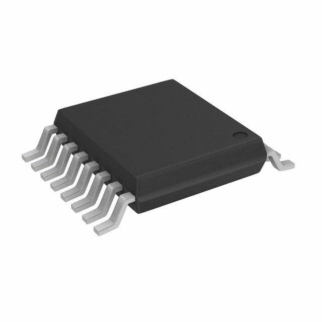
| 描述 | IC I/O EXPANDER SPI 8B 16TSSOP接口-I/O扩展器 8 Bit SPI GPIO Expander |
| 产品分类 | |
| I/O数 | 8 |
| 品牌 | Exar Corporation |
| 产品手册 | http://www.exar.com/interface/uart-and-bridging-solutions/bridging-solutions/spi-gpio-expanders/XRA1404/ |
| 产品图片 |
|
| rohs | 符合RoHS无铅 / 符合限制有害物质指令(RoHS)规范要求 |
| 产品系列 | 接口 IC,接口-I/O扩展器,Exar XRA1404IG16-F- |
| 数据手册 | http://www.exar.com/Common/Content/Document.ashx?id=20779 |
| 产品型号 | XRA1404IG16-F |
| 中断输出 | 是 |
| 产品种类 | 接口-I/O扩展器 |
| 供应商器件封装 | 16-TSSOP |
| 其它名称 | 1016-1725-5 |
| 功率耗散 | 200 mW |
| 包装 | 管件 |
| 商标 | Exar |
| 安装类型 | 表面贴装 |
| 安装风格 | SMD/SMT |
| 封装/外壳 | 16-TSSOP(0.173",4.40mm 宽) |
| 封装/箱体 | TSSOP-16 |
| 工作温度 | -40°C ~ 85°C |
| 工作温度范围 | - 40 C to + 85 C |
| 工作电源电压 | 1.65 V to 3.6 V |
| 工厂包装数量 | 95 |
| 接口 | SPI |
| 最大工作频率 | 15 MHz |
| 标准包装 | 95 |
| 特性 | - |
| 电压-电源 | 1.65 V ~ 3.6 V |
| 电流-灌/拉输出 | - |
| 输出电流 | 160 mA |
| 输出类型 | 开路漏极 |
| 频率-时钟 | 26MHz |


PDF Datasheet 数据手册内容提取
XRA1404 8-BIT SPI GPIO EXPANDER WITH INTEGRATED LEVEL SHIFTERS SEPTEMBER 2011 REV. 1.0.0 GENERAL DESCRIPTION FEATURES The XRA1404 is an 8-bit GPIO expander with an SPI • 1.65V to 3.6V operating voltage interface. After power-up, the XRA1404 has internal • Integrated level shifters 100K ohm pull-up resistors on each I/O pin that can be individually enabled. • 8 General Purpose I/Os (GPIOs) In addition, the GPIOs on the XRA1404 can • 5V tolerant inputs individually be controlled and configured. As outputs, • Maximum stand-by current of 1uA at +1.8V the GPIOs can be outputs that are high, low or in three-state mode. The three-state mode feature is • SPI bus interface useful for applications where the power is removed ■ SPI Clock Frequency up to 26MHz from the remote devices, but they may still be • Individually programmable inputs connected to the GPIO expander. ■ Internal pull-up resistors As inputs, the internal pull-up resistors can be enabled or disabled and the input polarity can be ■ Polarity inversion inverted. The interrupt can be programmed for ■ Individual interrupt enable different behaviors. The interrupts can be ■ Rising edge and/or Falling edge interrupt programmed to generate an interrupt on the rising ■ Input filter edge, falling edge or on both edges. The interrupt can be cleared if the input changes back to its original • Individually programmable outputs state or by reading the current state of the inputs. ■ Output Level Control The XRA1404 is available in 16-pin QFN and 16-pin ■ Output Three-State Control TSSOP packages. • Open-drain active low interrupt output • Active-low reset input • 3kV HBM ESD protection per JESD22-A114F • 200mA latch-up performance per JESD78B APPLICATIONS • Personal Digital Assistants (PDA) • Cellular Phones/Data Devices • Battery-Operated Devices • Global Positioning System (GPS) • Bluetooth Exar Corporation 48720 Kato Road, Fremont CA, 94538 • (510) 668-7000 • FAX (510) 668-7017 • www.exar.com
XRA1404 8-BIT SPI GPIO EXPANDER WITH INTEGRATED LEVEL SHIFTERS REV. 1.0.0 FIGURE 1. XRA1404 BLOCK DIAGRAM VCC (1.65V – 3.6V) (1.65V – 3.6V) VCCP CS# P0 P1 SCL P2 SI SPI Bus GPIO Integrated P3 Control GPIOs Level SO Interface P4 Registers Shifters P5 P6 P7 IRQ# GND ORDERING INFORMATION NUMBER OF OPERATING TEMPERATURE PART NUMBER PACKAGE DEVICE STATUS GPIOS RANGE XRA1404IL16-F QFN-16 8 -40°C to +85°C Active XRA1404IL16TR-F QFN-16 8 -40°C to +85°C Active XRA1404IG16-F TSSOP-16 8 -40°C to +85°C Active XRA1404IG16TR-F TSSOP-16 8 -40°C to +85°C Active NOTE: TR = Tape and Reel, F = Green / RoHS FIGURE 2. PIN OUT ASSIGNMENTS - XRA1404 P # C C S C C O VCC 1 16 VCCP C V V S CS# 2 15 SO 16 15 14 13 SI 1 12 SCL SI 3 14 SCL P0 2 XRA1404 11 IRQ# P0 4 XRA1404 13 IRQ# P1 3 16-Pin QFN 10 P7 P1 5 16-Pin TSSOP 12 P7 P2 4 9 P6 P2 6 11 P6 5 6 7 8 3 D 4 5 P3 7 10 P5 P N P P G GND 8 9 P4 2
XRA1404 REV. 1.0.0 8-BIT SPI GPIO EXPANDER WITH INTEGRATED LEVEL SHIFTERS PIN DESCRIPTIONS Pin Description QFN-16 TSSOP-16 NAME TYPE DESCRIPTION PIN# PIN# SPI INTERFACE SO 13 15 O SPI serial data output. SCL 12 14 I SPI serial input clock. IRQ# 11 13 OD Interrupt output (open-drain, active LOW). CS# 16 2 I SPI bus chip select. SI 1 3 I SPI serial data input. GPIOs P0 2 4 I/O General purpose I/Os P0-P7. All GPIOs are configured as inputs upon power- P1 3 5 I/O up or after a reset. P2 4 6 I/O P3 5 7 I/O P4 7 9 I/O P5 8 10 I/O P6 9 11 I/O P7 10 12 I/O ANCILLARY SIGNALS VCCP 14 16 Pwr 1.65V to 3.6V VCC supply voltage for GPIOs. VCC 15 1 Pwr 1.65V to 3.6V VCC supply voltage for SPI bus interface. GND 6 8 Pwr Power supply common, ground. GND Center - Pwr The exposed pad at the bottom surface of the package is designed for thermal Pad performance. Use of a center pad on the PCB is strongly recommended for ther- mal conductivity as well as to provide mechanical stability of the package on the PCB. The center pad is recommended to be solder masked defined with open- ing size less than or equal to the exposed thermal pad on the package bottom to prevent solder bridging to the outer leads of the device. Thermal vias must be connected to GND plane as the thermal pad of package is at GND potential. Pin type: I=Input, O=Output, I/O= Input/output, OD=Output Open Drain. 3
XRA1404 8-BIT SPI GPIO EXPANDER WITH INTEGRATED LEVEL SHIFTERS REV. 1.0.0 1.0 FUNCTIONAL DESCRIPTIONS 1.1 SPI bus Interface The SPI interface consists of four lines: serial clock (SCL), chip select (CS#), slave output (SO) and slave input (SI). The serial clock, slave output and slave input can be as fast as 26 MHz. To access the device in the SPI mode, the CS# signal is asserted by the SPI master, then the SPI master starts toggling the SCL signal with the appropriate transaction information. The first bit sent by the SPI master includes whether it is a read or write transaction and the register being accessed. See Table 1 below. TABLE 1: SPI COMMAND BYTE FORMAT BIT FUNCTION 7 Read/Write# Logic 1 = Read Logic 0 = Write 6:1 Command Byte 0 Reserved FIGURE 3. SPI WRITE SCL SI 0 0 0 A3 A2 A1 A0 X D7 D6 D5 D4 D3 D2 D1 D0 FIGURE 4. SPI READ SCL SI 1 0 0 A3 A2 A1 A0 X SO D7 D6 D5 D4 D3 D2 D1 D0 After the last read or write transaction, the SPI master will set the SCL signal back to its idle state (LOW). 4
XRA1404 REV. 1.0.0 8-BIT SPI GPIO EXPANDER WITH INTEGRATED LEVEL SHIFTERS 1.1.1 SPI Command Byte An SPI command byte is sent by the SPI master following the slave address. The command byte indicates the address offset of the register that will be accessed. Table 2 below lists the command bytes for each register. TABLE 2: COMMAND BYTE (REGISTER ADDRESS) COMMAND BYTE REGISTER NAME DESCRIPTION READ/WRITE DEFAULT VALUES 0x00 GSR - GPIO State Read-Only 0xXX 0x01 OCR - Output Control Read/Write 0xFF 0x02 PIR - Input Polarity Inversion Read/Write 0x00 0x03 GCR - GPIO Configuration Read/Write 0xFF 0x04 PUR - Input Internal Pull-up Resistor Enable/Disable Read/Write 0x00 0x05 IER - Input Interrupt Enable Read/Write 0x00 0x06 TSCR - Output Three-State Control Read/Write 0x00 0x07 ISR - Input Interrupt Status Read 0x00 0x08 REIR - Input Rising Edge Interrupt Enable Read/Write 0x00 0x09 FEIR - Input Falling Edge Interrupt Enable Read/Write 0x00 0x0A IFR - Input Filter Enable/Disable Read/Write 0xFF 1.2 Interrupts The table below summarizes the interrupt behavior of the different register settings for the XRA1404. TABLE 3: INTERRUPT GENERATION AND CLEARING GCR IER REIR FEIR IFR INTERRUPT GENERATED BY: INTERRUPT CLEARED BY: BIT BIT BIT BIT BIT 1 0 X X X No interrupts enabled (default) N/A 0 A rising or falling edge on the input Reading the GSR register or if the input changes back to its previous state (state of 1 1 0 0 1 A rising or falling edge on the input and input during last read to GSR) remains in the new state for more than 1075ns 0 A rising edge on the input Reading the GSR register 1 1 1 0 1 A rising edge on the input and remains high for more than 1075ns 0 A falling edge on the input Reading the GSR register 1 1 0 1 1 A falling edge on the input and remains low for more than 1075ns 0 A rising or falling edge on the input Reading the GSR register 1 1 1 1 1 A rising or falling edge on the input and remains in the new state for more than 1075ns 0 x x x x No interrupts in output mode N/A 5
XRA1404 8-BIT SPI GPIO EXPANDER WITH INTEGRATED LEVEL SHIFTERS REV. 1.0.0 2.0 REGISTER DESCRIPTION 2.1 GPIO State Register (GSR) - Read-Only The status of P7 - P0 can be read via this register. A read will show the current state of these pins (or the inverted state of these pins if enabled via the PIR Register). Reading this register will clear an input interrupt (see Table 3 for complete details). Reading this register will also return the last value written to the OCR register for any pins that are configured as outputs (ie. this is not the same as the state of the actual output pin since the output pin can be in three-state mode). A write to this register has no effect. The MSB of this register corresponds with P7 and the LSB of this register corresponds with P0. 2.2 Output Control Register (OCR) - Read/Write When P7 - P0 are defined as outputs, they can be controlled by writing to this register. Reading this register will return the last value written to it, however, this value may not be the actual state of the output pin since these pins can be in three-state mode. The MSB of this register corresponds with P7 and the LSB of this register corresponds with P0. 2.3 Input Polarity Inversion Register (PIR) - Read/Write When P7 - P0 are defined as inputs, this register inverts the polarity of the input value read from the Input Port Register. If the corresponding bit in this register is set to ’1’, the value of this bit in the GSR Register will be the inverted value of the input pin. If the corresponding bit in this register is set to ’0’, the value of this bit in the GSR Register will be the actual value of the input pin. The MSB of this register corresponds with P7 and the LSB of this register corresponds with P0. 2.4 GPIO Configuration Register (GCR) - Read/Write This register configures the GPIOs as inputs or outputs. After power-up and reset, the GPIOs are inputs. Setting these bits to ’0’ will enable the GPIOs as outputs. Setting these bits to ’1’ will enable the GPIOs as inputs. The MSB of this register corresponds with P7 and the LSB of this register corresponds with P0. 2.5 Input Internal Pull-up Enable/Disable Register (PUR) - Read/Write This register enables/disables the internal pull-up resistors for an input. After power-up and reset, the internal pull-up resistors are disabled for the XRA1404. Writing a ’1’ to these bits will enable the internal pull-up resistors. Writing a ’0’ to these bits will disable the internal pull-up resistors. The MSB of this register corresponds with P7 and the LSB of this register corresponds with P0. 2.6 Input Interrupt Enable Register (IER) - Read/Write This register enables/disables the interrupts for an input. After power-up and reset, the interrupts are disabled. Writing a ’1’ to these bits will enable the interrupt for the corresponding input pins. See Table 3 for complete details of the interrupt behavior for various register settings. No interrupts are generated for outputs when GCR bit is 0. The MSB of this register corresponds with P7 and the LSB of this register corresponds with P0. 2.7 Output Three-State Control Register (TSCR) - Read/Write This register can enable/disable the three-state mode of an output. Writing a ’1’ to these bits will enable the three-state mode for the corresponding output pins. The MSB of this register corresponds with P7 and the LSB of this register corresponds with P0. 2.8 Input Interrupt Status Register (ISR) - Read-Only This register reports the input pins that have generated an interrupt. See Table 3 for complete details of the interrupt behavior for various register settings. The MSB of this register corresponds with P7 and the LSB of this register corresponds with P0. 6
XRA1404 REV. 1.0.0 8-BIT SPI GPIO EXPANDER WITH INTEGRATED LEVEL SHIFTERS 2.9 Input Rising Edge Interrupt Enable Register (REIR) - Read/Write Writing a ’1’ to these bits will enable the corresponding input to generate an interrupt on the rising edge. See Table 3 for complete details of the interrupt behavior for various register settings. The MSB of this register corresponds with P7 and the LSB of this register corresponds with P0. 2.10 Input Falling Edge Interrupt Enable Register (FEIR) - Read/Write Writing a ’1’ to these bits will enable the corresponding input to generate an interrupt on the falling edge. Writing a ’1’ to these bits will make that input generate an interrupt on the rising edge only. See Table 3 for complete details of the interrupt behavior for various register settings. The MSB of this register corresponds with P7 and the LSB of this register corresponds with P0. 2.11 Input Filter Enable Register (IFR) - Read/Write By default, the input filters are enabled (IFR = 0xFF). When the input filters are enabled, any pulse that is greater than 1075ns will generate an interrupt (if enabled). Pulses that are less than 225ns will be filtered and will not generate an interrupt. Pulses in between this range may or may not generate an interrupt. Writing a ’0’ to these bits will disable the input filter for the corresponding inputs. With the input filters disabled, any change on the inputs will generate an interrupt (if enabled). See Table 3 for complete details of the interrupt behavior for various register settings. The MSB of this register corresponds with P7 and the LSB of this register corresponds with P0. 7
XRA1404 8-BIT SPI GPIO EXPANDER WITH INTEGRATED LEVEL SHIFTERS REV. 1.0.0 ABSOLUTE MAXIMUM RATINGS Power supply voltage 3.6 Volts Supply current 160 mA Ground current 200 mA External current limit of each GPIO 25 mA Total current limit for GPIO[7:0] 100 mA Total supply current sourced by all GPIOs 160 mA Operating Temperature -40o to +85oC Storage Temperature -65o to +150oC Power Dissipation 200 mW TYPICAL PACKAGE THERMAL RESISTANCE DATA (MARGIN OF ERROR: ± 15%) Thermal Resistance (16-QFN) theta-ja = 40oC/W, theta-jc = 26oC/W Thermal Resistance (16-TSSOP) theta-ja = 105oC/W, theta-jc = 20oC/W 8
XRA1404 REV. 1.0.0 8-BIT SPI GPIO EXPANDER WITH INTEGRATED LEVEL SHIFTERS ELECTRICAL CHARACTERISTICS DC ELECTRICAL CHARACTERISTICS UNLESS OTHERWISE NOTED: TA = -40O TO +85OC, VCC IS 1.65V TO 3.6V LIMITS LIMITS LIMITS SYMBOL PARAMETER 1.8V ± 10% 2.5V ± 10% 3.3V ± 10% UNITS CONDITIONS MIN MAX MIN MAX MIN MAX V Input Low Voltage -0.3 0.2 -0.3 0.5 -0.3 0.8 V Note 1 IL V Input High Voltage 1.4 5.5 1.8 5.5 2.0 5.5 V Note 1 IH V Output Low Voltage 0.4 V I = 6 mA OL OL 0.4 V I = 4 mA OL 0.4 V I = 1.5 mA OL Note 2 & Note 4 V Output Low Voltage 0.5 0.5 0.5 V I = 8 mA OL OL Note 3 V Output High Voltage 2.0 V I = -4 mA OH OL 1.8 V I = -2 mA OL 1.4 V I = -0.2 mA OL Note 2 V Output High Voltage 2.6 V I = -8 mA OH OH 1.8 V I = -8 mA OH 1.2 V I = -8 mA OH Note 3 I Input Low Leakage Current ±10 ±10 ±10 uA IL I Input High Leakage Current ±10 ±10 ±10 uA IH C Input Pin Capacitance 5 5 5 pF IN I Power Supply Current 0.5 1.0 2.0 mA Test 1 CC I Power Supply Current 0.6 1.2 2.4 mA Test 2 CC I Standby Current 1 2 5 uA Test 3 CCS RGPIO GPIO pull-up resistance 60 140 60 140 60 140 kΩ 100kΩ ± 40% NOTE: The Vcc comes from VCCP pin for the GPIOs and the VCC pin for the other signals; NOTES: 1. For SPI input signals (SI, SCL) & GPIOs, A0, A1 and A2 signals; 2. For SPI output signal SO; 3. For GPIOs; 4. For IRQ# signal; Test 1: SCL frequency is 10 MHz with internal pull-ups disabled. All GPIOs are configured as inputs. All inputs are steady at VCC or GND. Outputs are floating or in the tri-state mode. Test 2: SCL frequency is 10 MHz with internal pull-ups enabled. All GPIOs are configured as inputs. All inputs are steady at VCC or GND. Outputs are floating or in the tri-state mode. 9
XRA1404 8-BIT SPI GPIO EXPANDER WITH INTEGRATED LEVEL SHIFTERS REV. 1.0.0 Test 3: All inputs are steady at VCC or GND to minimize standby current. If internal pull-up is enabled, input voltage level should be the same as VCC. SCL and SI are at GND. CS# is at VCC. All GPIOs are configured as inputs. Outputs are left floating or in tri-state mode. AC ELECTRICAL CHARACTERISTICS - SPI-BUS TIMING SPECIFICATIONS Unless otherwise noted: TA=-40o to +85oC, Vcc=1.65V - 3.6V LIMITS LIMITS LIMITS SYMBOL PARAMETER 1.8V ± 10% 2.5V ± 10% 3.3V ± 10% UNIT CONDITIONS MIN MAX MIN MAX MIN MAX f Operating frequency 15 26 26 MHz SCL T CS# to SCL setup time 20 20 20 ns CSS T CS# to SCL hold time 20 20 20 ns CSH T SCL fall to SO valid time 100 100 100 ns C = 30 pF DO L T SI to SCL setup time 20 20 20 ns DS T SI to SCL hold time 20 20 20 ns DH T SCL period 66 38 38 ns T + T CP CH CL T SCL HIGH time 30 15 15 ns CH T SCL LOW time 30 15 15 ns CL T CS# HIGH pulse width 30 30 30 ns CSW T SPI input pin interrupt clear 200 200 200 ns D13 NOTE: The Vcc comes from the VCC pin. 10
XRA1404 REV. 1.0.0 8-BIT SPI GPIO EXPANDER WITH INTEGRATED LEVEL SHIFTERS FIGURE 5. SPI-BUS TIMING CS# ... TCSH TCSS TCL TCH TCSH TCSW SCLK ... TDH TDS SI ... TDO TTR ... SO FIGURE 6. READ INPUT PORT TO CLEAR GPIO INT CS# SCL SI 1 0 0 A3 A2 A1 A0 X SO D7 D6 D5 D4 D3 D2 D1 D0 TD13 INT# 11
XRA1404 8-BIT SPI GPIO EXPANDER WITH INTEGRATED LEVEL SHIFTERS REV. 1.0.0 PACKAGE DIMENSIONS (16 PIN QFN - 3 X 3 X 0.9 mm) θ Note: the actual center pad is metallic and the size (D2) is device-dependent with a typical tolerance of 0.3mm Note: The control dimension is in millimeter. INCHES MILLIMETERS SYMBOL MIN MAX MIN MAX A 0.031 0.039 0.80 1.00 A1 0.000 0.002 0.00 0.05 A3 0.000 0.008 0.00 0.20 D 0.118 BSC 3.00 BSC D2 0.063 0.071 1.60 1.80 b 0.010 0.014 0.25 0.35 e 0.020 BSC 0.50 BSC L 0.012 0.020 0.30 0.50 θ 0 14o 0 14o k 0.008 - 0.20 - 12
XRA1404 REV. 1.0.0 8-BIT SPI GPIO EXPANDER WITH INTEGRATED LEVEL SHIFTERS PACKAGE DIMENSIONS (16 PIN TSSOP - 4.4 mm) Note: The control dimension is in millimeter. INCHES MILLIMETERS SYMBOL MIN MAX MIN MAX A 0.031 0.047 0.80 1.20 A1 0.002 0.006 0.05 0.15 A2 0.031 0.037 0.80 0.95 b 0.007 0.012 0.19 0.30 C 0.004 0.008 0.09 0.2 D 0.193 0.201 4.90 5.10 E 0.240 0.264 6.30 6.60 E1 0.169 0.177 4.30 4.50 e 0.0256 BSC 0.65 BSC L 0.018 0.030 0.45 0.75 α 0° 8° 0° 8° 13
XRA1404 8-BIT SPI GPIO EXPANDER WITH INTEGRATED LEVEL SHIFTERS REV. 1.0.0 REVISION HISTORY DATE REVISION DESCRIPTION September 2011 1.0.0 Final Datasheet. NOTICE EXAR Corporation reserves the right to make changes to the products contained in this publication in order to improve design, performance or reliability. EXAR Corporation assumes no responsibility for the use of any circuits described herein, conveys no license under any patent or other right, and makes no representation that the circuits are free of patent infringement. Charts and schedules contained here in are only for illustration purposes and may vary depending upon a user’s specific application. While the information in this publication has been carefully checked; no responsibility, however, is assumed for inaccuracies. EXAR Corporation does not recommend the use of any of its products in life support applications where the failure or malfunction of the product can reasonably be expected to cause failure of the life support system or to significantly affect its safety or effectiveness. Products are not authorized for use in such applications unless EXAR Corporation receives, in writing, assurances to its satisfaction that: (a) the risk of injury or damage has been minimized; (b) the user assumes all such risks; (c) potential liability of EXAR Corporation is adequately protected under the circumstances. Copyright 2011 EXAR Corporation Datasheet September 2011. Send your UART technical inquiry with technical details to hotline: uarttechsupport@exar.com. Reproduction, in part or whole, without the prior written consent of EXAR Corporation is prohibited. 14