ICGOO在线商城 > 分立半导体产品 > 二极管 - 齐纳 - 单 > MMSZ2V7T1G
 Datasheet下载
- 型号: MMSZ2V7T1G
- 制造商: ON Semiconductor
- 库位|库存: xxxx|xxxx
- 要求:
| 数量阶梯 | 香港交货 | 国内含税 |
| +xxxx | $xxxx | ¥xxxx |
查看当月历史价格
查看今年历史价格
MMSZ2V7T1G产品简介:
ICGOO电子元器件商城为您提供MMSZ2V7T1G由ON Semiconductor设计生产,在icgoo商城现货销售,并且可以通过原厂、代理商等渠道进行代购。 MMSZ2V7T1G价格参考¥0.19-¥1.67。ON SemiconductorMMSZ2V7T1G封装/规格:二极管 - 齐纳 - 单, Zener Diode 2.7V 500mW ±5% Surface Mount SOD-123。您可以下载MMSZ2V7T1G参考资料、Datasheet数据手册功能说明书,资料中有MMSZ2V7T1G 详细功能的应用电路图电压和使用方法及教程。
MMSZ2V7T1G是ON Semiconductor(安森美半导体)生产的一款单个齐纳二极管,其主要应用场景如下:

 1. 电压稳压
MMSZ2V7T1G的齐纳击穿电压为2.7V,适用于需要稳定电压的电路中。它可以在电源波动较大的情况下,保持输出电压的稳定性,广泛应用于低压稳压电路、参考电压源等场合。例如,在传感器模块、微控制器供电电路中,它可以作为参考电压源,确保系统的电压稳定。

 2. 过压保护
该二极管可以用于防止电路中的瞬态高压对敏感元件造成损坏。当输入电压超过设定的齐纳电压时,齐纳二极管会导通,将多余的电流分流到地,从而保护后续电路。这种应用常见于电源输入端、通信接口等容易受到电压冲击的地方。

 3. 信号箝位
在模拟信号处理电路中,MMSZ2V7T1G可以用作信号箝位器件,限制信号的峰值电压,防止信号超出允许范围。例如,在音频放大器、射频电路中,它可以确保信号不会因为过大的幅度而失真或损坏电路。

 4. 温度补偿
由于齐纳二极管的击穿电压会随温度变化,MMSZ2V7T1G也可以用于温度补偿电路中。通过与其他温度敏感元件配合,它可以抵消温度变化对电路性能的影响,确保电路在不同环境温度下依然能够正常工作。

 5. 电源监控与复位电路
在一些嵌入式系统中,MMSZ2V7T1G可以用于电源监控电路,检测电源电压是否低于某个阈值,并触发复位信号。这种应用常见于单片机、DSP等处理器的复位电路中,确保系统在电源异常时能够自动重启。

总之,MMSZ2V7T1G凭借其稳定的齐纳电压特性,广泛应用于各种需要电压稳压、过压保护、信号箝位和温度补偿的电路中,尤其适合低压、小电流的应用场景。
| 参数 | 数值 |
| 产品目录 | |
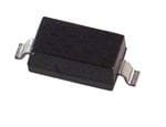
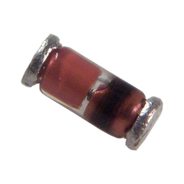
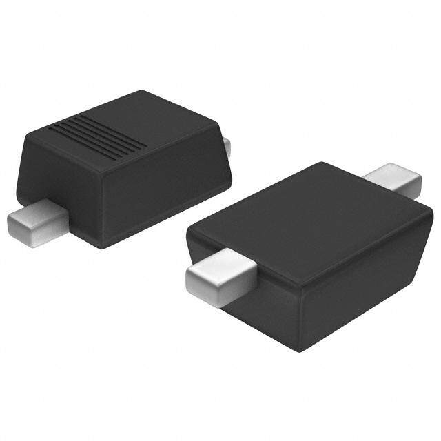
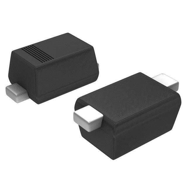
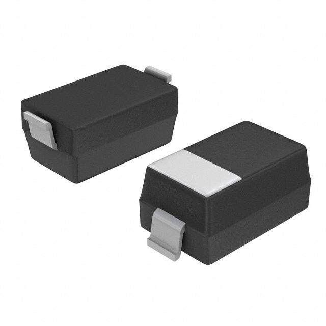
| 描述 | DIODE ZENER 2.7V 500MW SOD123 |
| 产品分类 | 单二极管/齐纳 |
| 品牌 | ON Semiconductor |
| 数据手册 | |
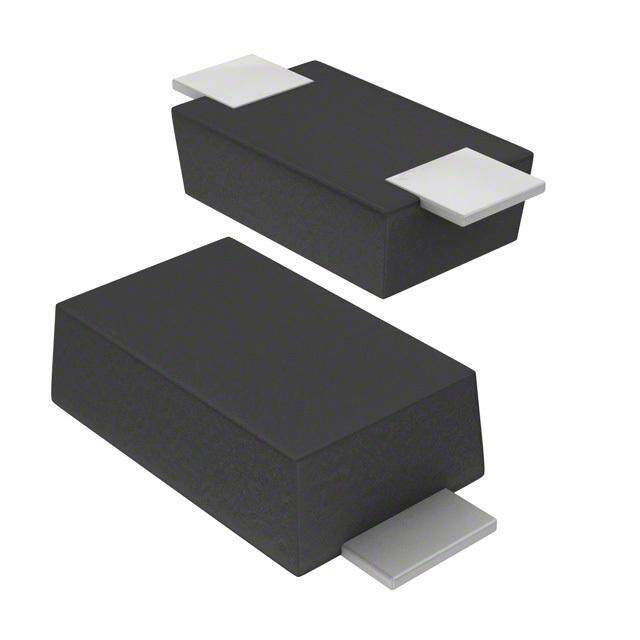
| 产品图片 |
|
| 产品型号 | MMSZ2V7T1G |
| PCN组件/产地 | |
| PCN设计/规格 | |
| rohs | 无铅 / 符合限制有害物质指令(RoHS)规范要求 |
| 产品系列 | - |
| 不同If时的电压-正向(Vf) | 900mV @ 10mA |
| 不同 Vr时的电流-反向漏电流 | 20µA @ 1V |
| 供应商器件封装 | SOD-123 |
| 其它名称 | MMSZ2V7T1GOSCT |
| 功率-最大值 | 500mW |
| 包装 | 剪切带 (CT) |
| 安装类型 | 表面贴装 |
| 容差 | ±5% |
| 封装/外壳 | SOD-123 |
| 工作温度 | -55°C ~ 150°C |
| 标准包装 | 1 |
| 电压-齐纳(标称值)(Vz) | 2.7V |
| 阻抗(最大值)(Zzt) | 100 欧姆 |


- 商务部:美国ITC正式对集成电路等产品启动337调查
- 曝三星4nm工艺存在良率问题 高通将骁龙8 Gen1或转产台积电
- 太阳诱电将投资9.5亿元在常州建新厂生产MLCC 预计2023年完工
- 英特尔发布欧洲新工厂建设计划 深化IDM 2.0 战略
- 台积电先进制程称霸业界 有大客户加持明年业绩稳了
- 达到5530亿美元!SIA预计今年全球半导体销售额将创下新高
- 英特尔拟将自动驾驶子公司Mobileye上市 估值或超500亿美元
- 三星加码芯片和SET,合并消费电子和移动部门,撤换高东真等 CEO
- 三星电子宣布重大人事变动 还合并消费电子和移动部门
- 海关总署:前11个月进口集成电路产品价值2.52万亿元 增长14.8%


PDF Datasheet 数据手册内容提取
MMSZxxxT1G Series, SZMMSZxxxT1G Series Zener Voltage Regulators 500 mW SOD−123 Surface Mount Three complete series of Zener diodes are offered in the convenient, http://onsemi.com surface mount plastic SOD−123 package. These devices provide a convenient alternative to the leadless 34−package style. Features 500 mW Rating on FR−4 or FR−5 Board Wide Zener Reverse Voltage Range − 2.4 V to 56 V Package Designed for Optimal Automated Board Assembly SOD−123 CASE 425 Small Package Size for High Density Applications STYLE 1 ESD Rating of Class 3 (> 16 kV) per Human Body Model AEC−Q101 Qualified and PPAP Capable SZ Prefix for Automotive and Other Applications Requiring Unique 1 2 Site and Control Change Requirements Cathode Anode Pb−Free Packages are Available* MARKING DIAGRAM Mechanical Characteristics CASE: Void-free, transfer-molded, thermosetting plastic case FINISH: Corrosion resistant finish, easily Solderable 1 xx M (cid:2) MAXIMUM CASE TEMPERATURE FOR SOLDERING PURPOSES: (cid:2) 260C for 10 Seconds POLARITY: Cathode indicated by polarity band FLAMMABILITY RATING: UL 94 V−0 xx = Device Code M = Date Code (cid:2) = Pb−Free Package MAXIMUM RATINGS (Note: Microdot may be in either location) Rating Symbol Max Unit Total Power Dissipation on FR−5 Board, PD ORDERING INFORMATION (Note 1) @ TL = 75C 500 mW Derated above 75C 6.7 mW/C Device Package Shipping† Thermal Resistance, Junction−to−Ambient R(cid:2)JA 340 C/W MMSZxxxT1G SOD−123 3,000 / (Note 2) (Pb−Free) Tape & Reel Thermal Resistance, Junction−to−Lead R(cid:2)JL 150 C/W SZMMSZxxxT1G SOD−123 3,000 / (Note 2) (Pb−Free) Tape & Reel MMSZxxxT3G SOD−123 10,000 / Junction and Storage Temperature Range TJ, Tstg −55 to +150 C (Pb−Free) Tape & Reel Stresses exceeding Maximum Ratings may damage the device. Maximum Ratings are stress ratings only. Functional operation above the Recommended SZMMSZxxxT3G SOD−123 10,000 / Operating Conditions is not implied. Extended exposure to stresses above the (Pb−Free) Tape & Reel Recommended Operating Conditions may affect device reliability. †For information on tape and reel specifications, 1. FR−5 = 3.5 X 1.5 inches. including part orientation and tape sizes, please 2. Thermal Resistance measurement obtained via infrared Scan Method. refer to our Tape and Reel Packaging Specifications Brochure, BRD8011/D. DEVICE MARKING INFORMATION See specific marking information in the device marking column of the Electrical Characteristics table on page 2 of this data sheet. *For additional information on our Pb−Free strategy and soldering details, please download the ON Semiconductor Soldering and Mounting Techniques Reference Manual, SOLDERRM/D. Semiconductor Components Industries, LLC, 2012 1 Publication Order Number: January, 2012 − Rev. 11 MMSZ2V4T1/D
MMSZxxxT1G Series, SZMMSZxxxT1G Series ELECTRICAL CHARACTERISTICS (TA = 25C unless I otherwise noted, VF = 0.95 V Max. @ IF = 10 mA) IF Symbol Parameter VZ Reverse Zener Voltage @ IZT IZT Reverse Current ZZT Maximum Zener Impedance @ IZT VZ VR V IR Reverse Leakage Current @ VR IIRZTVF VR Reverse Voltage IF Forward Current VF Forward Voltage @ IF Zener Voltage Regulator ELECTRICAL CHARACTERISTICS (TA = 25C unless otherwise noted, VF = 0.9 V Max. @ IF = 10 mA) VZ1 (Volts) ZZT1 VZ2 (Volts) ZZT2 Max Reverse (Notes 3 and 4) (Note 5) (Notes 3 and 4) (Note 5) Leakage Current Device @ IZT1 = 5 mA @ IZT2 = 1 mA IR @ VR Device* Marking Min Nom Max (cid:2) Min Max (cid:2) (cid:3)A Volts MMSZ2V4T1G T1 2.28 2.4 2.52 100 1.7 2.1 600 50 1 MMSZ2V7T1G T2 2.57 2.7 2.84 100 1.9 2.4 600 20 1 MMSZ3V0T1G T3 2.85 3.0 3.15 95 2.1 2.7 600 10 1 MMSZ3V3T1G T4 3.14 3.3 3.47 95 2.3 2.9 600 5 1 MMSZ3V6T1G T5 3.42 3.6 3.78 90 2.7 3.3 600 5 1 MMSZ3V9T1G U1 3.71 3.9 4.10 90 2.9 3.5 600 3 1 MMSZ4V3T1G U2 4.09 4.3 4.52 90 3.3 4.0 600 3 1 MMSZ4V7T1G U3 4.47 4.7 4.94 80 3.7 4.7 500 3 2 MMSZ5V1T1G U4 4.85 5.1 5.36 60 4.2 5.3 480 2 2 MMSZ5V6T1G/T3G U5 5.32 5.6 5.88 40 4.8 6.0 400 1 2 MMSZ6V2T1G V1 5.89 6.2 6.51 10 5.6 6.6 150 3 4 MMSZ6V8T1G V2 6.46 6.8 7.14 15 6.3 7.2 80 2 4 MMSZ7V5T1G V3 7.13 7.5 7.88 15 6.9 7.9 80 1 5 MMSZ8V2T1G V4 7.79 8.2 8.61 15 7.6 8.7 80 0.7 5 MMSZ9V1T1G V5 8.65 9.1 9.56 15 8.4 9.6 100 0.5 6 MMSZ10T1G A1 9.50 10 10.50 20 9.3 10.6 150 0.2 7 MMSZ11T1G A2 10.45 11 11.55 20 10.2 11.6 150 0.1 8 MMSZ12T1G A3 11.40 12 12.60 25 11.2 12.7 150 0.1 8 MMSZ13T1G A4 12.35 13 13.65 30 12.3 14.0 170 0.1 8 MMSZ15T1G A5 14.25 15 15.75 30 13.7 15.5 200 0.05 10.5 MMSZ16T1G X1 15.20 16 16.80 40 15.2 17.0 200 0.05 11.2 MMSZ18T1G/T3G X2 17.10 18 18.90 45 16.7 19.0 225 0.05 12.6 MMSZ20T1G X3 19.00 20 21.00 55 18.7 21.1 225 0.05 14 MMSZ22T1G X4 20.90 22 23.10 55 20.7 23.2 250 0.05 15.4 MMSZ24T1G X5 22.80 24 25.20 70 22.7 25.5 250 0.05 16.8 3. The type numbers shown have a standard tolerance of 5% on the nominal Zener Voltage. 4. Tolerance and Voltage Designation: Zener Voltage (VZ) is measured with the Zener Current applied for PW = 1 ms. 5. ZZT and ZZK are measured by dividing the AC voltage drop across the device by the AC current applied. The specified limits are for IZ(AC) = 0.1 IZ(DC), with the AC frequency = 1 kHz. *Include SZ-prefix devices where applicable. http://onsemi.com 2
MMSZxxxT1G Series, SZMMSZxxxT1G Series ELECTRICAL CHARACTERISTICS (TA = 25C unless otherwise noted, VF = 0.9 V Max. @ IF = 10 mA) VZ1 (Volts) ZZT1 VZ2 (Volts) ZZT2 Max Reverse (Notes 6 and 7) (Note 8) (Notes 6 and 7) (Note 8) Leakage Current @ IZT2 = Device @ IZT1 = 2 mA @ IZT2 = 0.1 mA 0.5 mA IR @ VR Device* Marking Min Nom Max (cid:2) Min Max (cid:2) (cid:3)A Volts MMSZ27T1G/T3G Y1 25.65 27 28.35 80 25 28.9 300 0.05 18.9 MMSZ30T1G Y2 28.50 30 31.50 80 27.8 32 300 0.05 21 MMSZ33T1G Y3 31.35 33 34.65 80 30.8 35 325 0.05 23.1 MMSZ36T1G Y4 34.20 36 37.80 90 33.8 38 350 0.05 25.2 MMSZ39T1G Y5 37.05 39 40.95 130 36.7 41 350 0.05 27.3 MMSZ43T1G Z1 40.85 43 45.15 150 39.7 46 375 0.05 30.1 MMSZ47T1G Z2 44.65 47 49.35 170 43.7 50 375 0.05 32.9 MMSZ51T1G Z3 48.45 51 53.55 180 47.6 54 400 0.05 35.7 MMSZ56T1G Z4 53.20 56 58.80 200 51.5 60 425 0.05 39.2 6. The type numbers shown have a standard tolerance of 5% on the nominal Zener Voltage. 7. Tolerance and Voltage Designation: Zener Voltage (VZ) is measured with the Zener Current applied for PW = 1 ms. 8. ZZT and ZZK are measured by dividing the AC voltage drop across the device by the AC current applied. The specified limits are for IZ(AC) = 0.1 IZ(DC), with the AC frequency = 1 kHz. *Include SZ-prefix devices where applicable. http://onsemi.com 3
MMSZxxxT1G Series, SZMMSZxxxT1G Series TYPICAL CHARACTERISTICS 8 100 C) C) mV/ 7 TYPICAL TC VALUES mV/ TFYOPRI CMAMLS TZCx xVxATL1UGE SSERIES, NT ( 6 FSOZMR MMSMZSxxZxxTx1xTG1 SGE SREIERSIES, NT ( SZMMSZxxxT1G SERIES E 5 E CI CI FFI 4 VZ @ IZT FFI VZ @ IZT E E O 3 O C C E E 10 R 2 R U U T T A 1 A R R E E P 0 P M M E −1 E T T , Z , Z V −2 V −3 1 2 3 4 5 6 7 8 9 10 11 12 10 100 VZ, NOMINAL ZENER VOLTAGE (V) VZ, NOMINAL ZENER VOLTAGE (V) Figure 1. Temperature Coefficients Figure 2. Temperature Coefficients (Temperature Range −55C to +150C) (Temperature Range −55C to +150C) 1.2 1000 1.0 ATTS) RWEACVTEAFNOGRUML, ATRA = 25C W R ( 0.8 PD versus TL E 100 W O P 0.6 E PD versus TA RG U S 0.4 K 10 A E P 0.2 , pk P 0 1 0 25 50 75 100 125 150 0.1 1 10 100 1000 T, TEMPERATURE (C) PW, PULSE WIDTH (ms) Figure 3. Steady State Power Derating Figure 4. Maximum Nonrepetitive Surge Power 1000 1000 TJ = 25C 75 V (MMSZ5267BT1G) ) IfZ =(A 1C )k H= z0.1 IZ(DC) A) 91 V (MMSZ5270BT1G) DANCE ( 100 IZ = 1 mA RENT (m 100 MPE 5 mA CUR C I D MI 20 mA AR A W DYN 10 OR 10 , ZT , FF Z I 150C 75C 25C 0C 1 1 1 10 100 0.4 0.5 0.6 0.7 0.8 0.9 1.0 1.1 1.2 VZ, NOMINAL ZENER VOLTAGE VF, FORWARD VOLTAGE (V) Figure 5. Effect of Zener Voltage on Figure 6. Typical Forward Voltage Zener Impedance http://onsemi.com 4
MMSZxxxT1G Series, SZMMSZxxxT1G Series TYPICAL CHARACTERISTICS 1000 1000 TA = 25C A) 0 V BIAS 100 T ( 1 V BIAS N E 10 E (pF) 100 CURR 1 CAPACITANC 10 B50IA%S O AFT VZ NOM , LEAKAGE R0.00.11 +150C C, I0.001 +25C −55C 0.0001 1 0.00001 1 10 100 0 10 20 30 40 50 60 70 80 90 VZ, NOMINAL ZENER VOLTAGE (V) VZ, NOMINAL ZENER VOLTAGE (V) Figure 7. Typical Capacitance Figure 8. Typical Leakage Current 100 100 TA = 25C TA = 25C mA) 10 mA) 10 T ( T ( N N E E R R R R U 1 U 1 C C R R E E N N E E Z Z , Z 0.1 , Z0.1 I I 0.01 0.01 0 2 4 6 8 10 12 10 30 50 70 90 VZ, ZENER VOLTAGE (V) VZ, ZENER VOLTAGE (V) Figure 9. Zener Voltage versus Zener Current Figure 10. Zener Voltage versus Zener Current (V Up to 12 V) (12 V to 91 V) Z http://onsemi.com 5
MMSZxxxT1G Series, SZMMSZxxxT1G Series PACKAGE DIMENSIONS SOD−123 CASE 425−04 ISSUE G D A NOTES: 1.DIMENSIONING AND TOLERANCING PER ANSI A1 Y14.5M, 1982. 2.CONTROLLING DIMENSION: INCH. ÂÂÂ1 Â MILLIMETERS INCHES ÂÂÂÂ DIM MIN NOM MAX MIN NOM MAX A 0.94 1.17 1.35 0.037 0.046 0.053 A1 0.00 0.05 0.10 0.000 0.002 0.004 b 0.51 0.61 0.71 0.020 0.024 0.028 HE E c --- --- 0.15 --- --- 0.006 D 1.40 1.60 1.80 0.055 0.063 0.071 E 2.54 2.69 2.84 0.100 0.106 0.112 HE 3.56 3.68 3.86 0.140 0.145 0.152 L 0.25 --- --- 0.010 --- --- (cid:4) 0 --- 10 0 --- 10 2 (cid:4) STYLE 1: PIN 1. CATHODE b L 2. ANODE C SOLDERING FOOTPRINT* 0.91 0.036 ÉÉ ÉÉ 1.22 ÉÉ ÉÉ 0.048 ÉÉ ÉÉ 2.36 0.093 4.19 0.165 (cid:2) (cid:3) mm SCALE 10:1 inches *For additional information on our Pb−Free strategy and soldering details, please download the ON Semiconductor Soldering and Mounting Techniques Reference Manual, SOLDERRM/D. ON Semiconductor and are registered trademarks of Semiconductor Components Industries, LLC (SCILLC). SCILLC reserves the right to make changes without further notice to any products herein. SCILLC makes no warranty, representation or guarantee regarding the suitability of its products for any particular purpose, nor does SCILLC assume any liability arising out of the application or use of any product or circuit, and specifically disclaims any and all liability, including without limitation special, consequential or incidental damages. “Typical” parameters which may be provided in SCILLC data sheets and/or specifications can and do vary in different applications and actual performance may vary over time. All operating parameters, including “Typicals” must be validated for each customer application by customer’s technical experts. SCILLC does not convey any license under its patent rights nor the rights of others. SCILLC products are not designed, intended, or authorized for use as components in systems intended for surgical implant into the body, or other applications intended to support or sustain life, or for any other application in which the failure of the SCILLC product could create a situation where personal injury or death may occur. Should Buyer purchase or use SCILLC products for any such unintended or unauthorized application, Buyer shall indemnify and hold SCILLC and its officers, employees, subsidiaries, affiliates, and distributors harmless against all claims, costs, damages, and expenses, and reasonable attorney fees arising out of, directly or indirectly, any claim of personal injury or death associated with such unintended or unauthorized use, even if such claim alleges that SCILLC was negligent regarding the design or manufacture of the part. SCILLC is an Equal Opportunity/Affirmative Action Employer. This literature is subject to all applicable copyright laws and is not for resale in any manner. PUBLICATION ORDERING INFORMATION LITERATURE FULFILLMENT: N. American Technical Support: 800−282−9855 Toll Free ON Semiconductor Website: www.onsemi.com Literature Distribution Center for ON Semiconductor USA/Canada P.O. Box 5163, Denver, Colorado 80217 USA Europe, Middle East and Africa Technical Support: Order Literature: http://www.onsemi.com/orderlit Phone: 303−675−2175 or 800−344−3860 Toll Free USA/Canada Phone: 421 33 790 2910 Fax: 303−675−2176 or 800−344−3867 Toll Free USA/Canada Japan Customer Focus Center For additional information, please contact your local Email: orderlit@onsemi.com Phone: 81−3−5817−1050 Sales Representative http://onsemi.com MMSZ2V4T1/D 6
Mouser Electronics Authorized Distributor Click to View Pricing, Inventory, Delivery & Lifecycle Information: O N Semiconductor: MMSZ10T1 MMSZ10T3 MMSZ10T3G MMSZ11T1 MMSZ12T1 MMSZ12T3G MMSZ13T1 MMSZ15T1 MMSZ15T1G MMSZ15T3G MMSZ16T1 MMSZ18T1 MMSZ20T1 MMSZ22T1 MMSZ22T3G MMSZ24T1 MMSZ27T1 MMSZ27T3 MMSZ2V4T1 MMSZ2V4T3G MMSZ2V7T1 MMSZ2V7T1G MMSZ2V7T3G MMSZ30T1 MMSZ33T1 MMSZ33T3G MMSZ36T1 MMSZ39T1 MMSZ3V0T1 MMSZ3V3T1 MMSZ3V3T3 MMSZ3V6T1 MMSZ3V6T3G MMSZ3V9T1 MMSZ43T1 MMSZ47T3G MMSZ4V3T1 MMSZ4V7T1 MMSZ4V7T3 MMSZ4V7T3G MMSZ51T1 MMSZ56T1 MMSZ5V1T1 MMSZ5V1T1G MMSZ5V1T3 MMSZ5V1T3G MMSZ5V6T1 MMSZ6V2T1 MMSZ6V8T1 MMSZ6V8T3G MMSZ7V5T1 MMSZ8V2T1 MMSZ8V2T3 MMSZ8V2T3G MMSZ9V1T1 MMSZ9V1T3 SZMMSZ5V1T1G