ICGOO在线商城 > 集成电路(IC) > 接口 - I/O 扩展器 > XRA1201PIG24-F

 Datasheet下载
- 型号: XRA1201PIG24-F
- 制造商: Exar
- 库位|库存: xxxx|xxxx
- 要求:
| 数量阶梯 | 香港交货 | 国内含税 |
| +xxxx | $xxxx | ¥xxxx |
查看当月历史价格
查看今年历史价格
XRA1201PIG24-F产品简介:
ICGOO电子元器件商城为您提供XRA1201PIG24-F由Exar设计生产,在icgoo商城现货销售,并且可以通过原厂、代理商等渠道进行代购。 XRA1201PIG24-F价格参考。ExarXRA1201PIG24-F封装/规格:接口 - I/O 扩展器, I/O Expander 16 I²C, SMBus 400kHz 24-TSSOP。您可以下载XRA1201PIG24-F参考资料、Datasheet数据手册功能说明书,资料中有XRA1201PIG24-F 详细功能的应用电路图电压和使用方法及教程。
MaxLinear, Inc. 的 XRA1201PIG24-F 是一款接口 I/O 扩展器,广泛应用于需要高效、灵活的 GPIO(通用输入输出)扩展和信号管理的场景。以下是其主要应用场景:

 1. 工业自动化
   - 在工业控制系统中,XRA1201PIG24-F 可用于扩展 PLC(可编程逻辑控制器)或嵌入式设备的 GPIO 接口,支持更多的传感器、执行器或其他外设连接。
   - 提供高可靠性信号传输,适用于恶劣环境下的工业通信。

 2. 智能家居与物联网 (IoT)
   - 该器件可用于智能家居网关或 IoT 网关中,扩展连接各种传感器(如温度、湿度、光照等)和控制模块(如继电器、LED 指示灯等)。
   - 支持多路输入/输出控制,满足智能照明、安防监控等应用需求。

 3. 消费电子
   - 在消费类电子产品中(如电视、机顶盒、音频设备等),XRA1201PIG24-F 可用于扩展按键检测、状态指示灯控制等功能。
   - 提供低功耗设计,适合便携式或电池供电设备。

 4. 汽车电子
   - 在车载系统中,这款 I/O 扩展器可以用于车身控制模块(BCM)、信息娱乐系统或 ADAS(高级驾驶辅助系统)中,扩展对开关、按钮、指示灯等的控制能力。
   - 其高抗干扰性能确保在复杂电磁环境下稳定运行。

 5. 医疗设备
   - 医疗仪器中常需要精确的信号采集与控制,XRA1201PIG24-F 可用于扩展患者监护仪、呼吸机等设备的 I/O 功能。
   - 支持多种工作模式,适应不同的医疗应用场景。

 6. 通信设备
   - 在路由器、交换机或其他网络设备中,该芯片可用于扩展端口状态监测、电源管理等功能。
   - 提供灵活的配置选项,简化开发流程。

 核心优势:
- 低功耗:适合对能效要求较高的应用。
- 宽电压范围:兼容多种电源环境。
- 高集成度:减少 PCB 占用面积,降低系统复杂性。
- 多种通信接口:支持 SPI/I²C 等主流协议,便于与主控 MCU 配合使用。

总之,XRA1201PIG24-F 凭借其高性能和灵活性,成为众多需要 I/O 扩展解决方案的应用领域的理想选择。
| 参数 | 数值 |
| 产品目录 | 集成电路 (IC)半导体 |
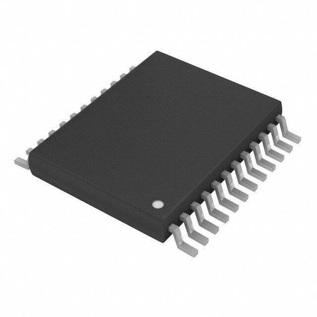
| 描述 | IC I/O EXPANDER I2C 16B 24TSSOP接口-I/O扩展器 16 Bit I2C SMBus GPIO Expander |
| 产品分类 | |
| I/O数 | 16 |
| 品牌 | Exar Corporation |
| 产品手册 | http://www.exar.com/interface/uart-and-bridging-solutions/bridging-solutions/i2c-gpio-expanders/XRA1201/ |
| 产品图片 |
|
| rohs | 符合RoHS无铅 / 符合限制有害物质指令(RoHS)规范要求 |
| 产品系列 | 接口 IC,接口-I/O扩展器,Exar XRA1201PIG24-F- |
| 数据手册 | http://www.exar.com/Common/Content/Document.ashx?id=20780 |
| 产品型号 | XRA1201PIG24-F |
| 中断输出 | 是 |
| 产品种类 | 接口-I/O扩展器 |
| 供应商器件封装 | 24-TSSOP |
| 其它名称 | 1016-1711 |
| 功率耗散 | 200 mW |
| 包装 | 管件 |
| 商标 | Exar |
| 安装类型 | 表面贴装 |
| 安装风格 | SMD/SMT |
| 封装/外壳 | 24-TSSOP(0.173",4.40mm 宽) |
| 封装/箱体 | TSSOP-24 |
| 工作温度 | -40°C ~ 85°C |
| 工作温度范围 | - 40 C to + 85 C |
| 工作电源电压 | 1.65 V to 3.6 V |
| 工厂包装数量 | 62 |
| 接口 | I²C, SMBus |
| 接口类型 | I2C, SMBus |
| 最大工作频率 | 100 kHz |
| 标准包装 | 62 |
| 特性 | - |
| 电压-电源 | 1.65 V ~ 3.6 V |
| 电流-灌/拉输出 | - |
| 输出电流 | 160 mA |
| 输出类型 | 开路漏极 |
| 频率-时钟 | 400kHz |


- 商务部:美国ITC正式对集成电路等产品启动337调查
- 曝三星4nm工艺存在良率问题 高通将骁龙8 Gen1或转产台积电
- 太阳诱电将投资9.5亿元在常州建新厂生产MLCC 预计2023年完工
- 英特尔发布欧洲新工厂建设计划 深化IDM 2.0 战略
- 台积电先进制程称霸业界 有大客户加持明年业绩稳了
- 达到5530亿美元!SIA预计今年全球半导体销售额将创下新高
- 英特尔拟将自动驾驶子公司Mobileye上市 估值或超500亿美元
- 三星加码芯片和SET,合并消费电子和移动部门,撤换高东真等 CEO
- 三星电子宣布重大人事变动 还合并消费电子和移动部门
- 海关总署:前11个月进口集成电路产品价值2.52万亿元 增长14.8%


PDF Datasheet 数据手册内容提取
XRA1201/1201P 16-BIT I2C/SMBUS GPIO EXPANDER SEPTEMBER 2011 REV. 1.0.0 GENERAL DESCRIPTION FEATURES The XRA1201/1201P is a 16-bit GPIO expander with • 1.65V to 3.6V operating voltage an I2C/SMBus interface. After power-up, the • 16 General Purpose I/Os (GPIOs) XRA1201 has internal 100K ohm pull-up resistors on • 5V tolerant inputs each I/O pin that can be individually enabled. The XRA1201P has the internal pull-up resistors enabled • Maximum stand-by current of 1uA at +1.8V upon power-up in case it is necessary for the inputs • I2C/SMBus bus interface to be in a known state. In addition, the GPIOs on the XRA1201/1201P can ■ I2C clock frequency up to 400kHz individually be controlled and configured. As outputs, ■ Noise filter on SDA and SCL inputs the GPIOs can be outputs that are high, low or in ■ Up to 32 I2C Slave Addresses three-state mode. The three-state mode feature is useful for applications where the power is removed • Individually programmable inputs from the remote devices, but they may still be ■ Internal pull-up resistors connected to the GPIO expander. ■ Polarity inversion As inputs, the internal pull-up resistors can be ■ Individual interrupt enable enabled or disabled and the input polarity can be ■ Rising edge and/or Falling edge interrupt inverted. The interrupt can be programmed for different behaviors. The interrupts can be ■ Input filter programmed to generate an interrupt on the rising • Individually programmable outputs edge, falling edge or on both edges. The interrupt ■ Output Level Control can be cleared if the input changes back to its original state or by reading the current state of the inputs. ■ Output Three-State Control The XRA1201/1201P are enhanced versions of other • Open-drain active low interrupt output 16-bit GPIO expanders with an I2C/SMBus interface. • Pin and software compatible with PCA9535, The XRA1201 is pin and software compatible with the TCA9535, MAX7312 (XRA1201) PCA9535, TCA9535 and MAX7312. The XRA1201P • Pin and software compatible with CAT9555, is pin and software compatible with the CAT9555, PCA9555, TCA9555, MAX7311 and MAX7318 PCA9555, TCA9555, MAX7311 and MAX7318. (XRA1201P) The XRA1201/1201P are available in 24-pin QFN • 3kV HBM ESD protection per JESD22-A114F and 24-pin TSSOP packages. • 200mA latch-up performance per JESD78B APPLICATIONS • Personal Digital Assistants (PDA) • Cellular Phones/Data Devices • Battery-Operated Devices • Global Positioning System (GPS) • Bluetooth Exar Corporation 48720 Kato Road, Fremont CA, 94538 • (510) 668-7000 • FAX (510) 668-7017 • www.exar.com
XRA1201/1201P 16-BIT I2C/SMBUS GPIO EXPANDER REV. 1.0.0 FIGURE 1. XRA1201 BLOCK DIAGRAM VCC (1.65V – 3.6V) P0 P1 P2 P3 GPIOs P4 P5 SCL P6 SDA P7 I2C/ GPIO A2 SMBus Control A1 Interface Registers A0 P8 P9 IRQ# P10 P11 GPIOs P12 P13 P14 GND P15 ORDERING INFORMATION NUMBER OF OPERATING TEMPERATURE PART NUMBER PACKAGE DEVICE STATUS GPIOS RANGE XRA1201IL24-F QFN-24 16 -40°C to +85°C Active XRA1201IL24TR-F QFN-24 16 -40°C to +85°C Active XRA1201PIL24-F QFN-24 16 -40°C to +85°C Active XRA1201PIL24TR-F QFN-24 16 -40°C to +85°C Active XRA1201IG24-F TSSOP-24 16 -40°C to +85°C Active XRA1201IG24TR-F TSSOP-24 16 -40°C to +85°C Active XRA1201PIG24-F TSSOP-24 16 -40°C to +85°C Active XRA1201PIG24TR-F TSSOP-24 16 -40°C to +85°C Active NOTE: TR = Tape and Reel, F = Green / RoHS FIGURE 2. PIN OUT ASSIGNMENTS IRQ# 1 24 VCC A2 A1 IRQ# VCC SDA SCL AA21 32 2223 SSDCAL 242322 21 20 19 P0 4 21 A0 P0 1 18 A0 P1 2 XRA1201/ 17 P15 P1 5 XRA1201/ 20 P15 P2 3 XRA1201P 16 P14 P2 6 XRA1201P 19 P14 P3 4 24-Pin QFN 15 P13 P3 7 T2S4S-POinP 18 P13 P4 5 14 P12 P4 8 17 P12 P5 6 13 P11 7 8 9 10 11 12 P5 9 16 P11 P6 P7 GND P8 P9 P10 P6 10 15 P10 P7 11 14 P9 GND 12 13 P8 2
XRA1201/1201P REV. 1.0.0 16-BIT I2C/SMBUS GPIO EXPANDER PIN DESCRIPTIONS Pin Description QFN-24 TSSOP-24 NAME TYPE DESCRIPTION PIN# PIN# I2C INTERFACE SDA 20 23 I/O I2C-bus data input/output (open-drain). SCL 19 22 I I2C-bus serial input clock. IRQ# 22 1 OD Interrupt output (open-drain, active LOW). A0 18 21 I These pins select the I2C slave address. See Table 1. A1 23 2 I A2 24 3 I GPIOs P0 1 4 I/O General purpose I/Os P0-P7. All GPIOs are configured as inputs upon power- P1 2 5 I/O up or after a reset. After power-up or reset, the internal pull-up resistors are P2 3 6 I/O enabled for the XRA1201P. The internal pull-up resistors are disabled for the XRA1201. P3 4 7 I/O P4 5 8 I/O P5 6 9 I/O P6 7 10 I/O P7 8 11 I/O P8 10 13 I/O General purpose I/O P8-P15. All GPIOs are configured as inputs upon power- P9 11 14 I/O up or after a reset. After power-up or reset, the internal pull-up resistors are P10 12 15 I/O enabled for the XRA1201P. The internal pull-up resistors are disabled for the XRA1201. P11 13 16 I/O P12 14 17 I/O P13 15 18 I/O P14 16 19 I/O P15 17 20 I/O ANCILLARY SIGNALS VCC 21 24 Pwr 1.65V to 3.6V VCC supply voltage. GND 9 12 Pwr Power supply common, ground. GND Center - Pwr The exposed pad at the bottom surface of the package is designed for thermal Pad performance. Use of a center pad on the PCB is strongly recommended for ther- mal conductivity as well as to provide mechanical stability of the package on the PCB. The center pad is recommended to be solder masked defined with open- ing size less than or equal to the exposed thermal pad on the package bottom to prevent solder bridging to the outer leads of the device. Thermal vias must be connected to GND plane as the thermal pad of package is at GND potential. Pin type: I=Input, O=Output, I/O= Input/output, OD=Output Open Drain. 3
XRA1201/1201P 16-BIT I2C/SMBUS GPIO EXPANDER REV. 1.0.0 1.0 FUNCTIONAL DESCRIPTIONS 1.1 I2C-bus Interface The I2C-bus interface is compliant with the Standard-mode and Fast-mode I2C-bus specifications. The I2C-bus interface consists of two lines: serial data (SDA) and serial clock (SCL). In the Standard-mode, the serial clock and serial data can go up to 100 kbps and in the Fast-mode, the serial clock and serial data can go up to 400 kbps. The first byte sent by an I2C-bus master contains a start bit (SDA transition from HIGH to LOW when SCL is HIGH), 7-bit slave address and whether it is a read or write transaction. The next byte is the sub-address that contains the address of the register to access. The XRA120x responds to each write with an acknowledge (SDA driven LOW by XRA1201/1201P for one clock cycle when SCL is HIGH). The last byte sent by an I2C- bus master contains a stop bit (SDA transition from LOW to HIGH when SCL is HIGH). See Figures 3 - 5 below. For complete details, see the I2C-bus specifications. FIGURE 3. I2C START AND STOP CONDITIONS SDA SCL S P START condition STOP condition FIGURE 4. MASTER WRITES TO SLAVE SLAVE COMMAND DATA S W A A A P ADDRESS BYTE BYTE White block: host to XRA120x Grey block: XRA120x to host FIGURE 5. MASTER READS FROM SLAVE SLAVE COMMAND SLAVE S W A A S R A nDATA A LAST DATA NA P ADDRESS BYTE ADDRESS White block: host to XRA120x Grey block: XRA120x to host 4
XRA1201/1201P REV. 1.0.0 16-BIT I2C/SMBUS GPIO EXPANDER 1.1.1 I2C-bus Addressing There could be many devices on the I2C-bus. To distinguish itself from the other devices on the I2C-bus, the XRA1201/1201P has up to 32 I2C slave addresses using the A2-A0 address lines. Table 1 below shows the different addresses that can be selected. TABLE 1: I2C ADDRESS MAP A2 A1 A0 I2C ADDRESS GND SCL GND 0x20 (0010 000X) GND SCL VCC 0x22 (0010 001X) GND SDA GND 0x24 (0010 010X) GND SDA VCC 0x26 (0010 011X) VCC SCL GND 0x28 (0010 100X) VCC SCL VCC 0x2A (0010 101X) VCC SDA GND 0x2C (0010 110X) VCC SDA VCC 0x2E (0010 111X) GND SCL SCL 0x30 (0011 000X) GND SCL SDA 0x32 (0011 001X) GND SDA SCL 0x34 (0011 010X) GND SDA SDA 0x36 (0011 011X) VCC SCL SCL 0x38 (0011 100X) VCC SCL SDA 0x3A (0011 101X) VCC SDA SCL 0x3C (0011 110X) VCC SDA SDA 0x3E (0011 111X) GND GND GND 0x40 (0100 000X) GND GND VCC 0x42 (0100 001X) GND VCC GND 0x44 (0100 010X) GND VCC VCC 0x46 (0100 011X) VCC GND GND 0x48 (0100 100X) VCC GND VCC 0x4A (0100 101X) VCC VCC GND 0x4C (0100 110X) VCC VCC VCC 0x4E (0100 111X) GND GND SCL 0x50 (0101 000X) GND GND SDA 0x52 (0101 001X) GND VCC SCL 0x54 (0101 010X) GND VCC SDA 0x56 (0101 011X) VCC GND SCL 0x58 (0101 100X) VCC GND SDA 0x5A (0101 101X) VCC VCC SCL 0x5C (0101 110X) VCC VCC SDA 0x5E (0101 111X) 5
XRA1201/1201P 16-BIT I2C/SMBUS GPIO EXPANDER REV. 1.0.0 1.1.2 I2C Read and Write A read or write transaction is determined by bit-0 of the slave address. If bit-0 is ’0’, then it is a write transaction. If bit-0 is ’1’, then it is a read transaction. 1.1.3 I2C Command Byte An I2C command byte is sent by the I2C master following the slave address. The command byte indicates the address offset of the register that will be accessed. Table 2 below lists the command bytes for each register. TABLE 2: I2C COMMAND BYTE (REGISTER ADDRESS) COMMAND BYTE REGISTER NAME DESCRIPTION READ/WRITE DEFAULT VALUES 0x00 GSR1 - GPIO State for P0-P7 Read-Only 0xXX 0x01 GSR2 - GPIO State for P8-P15 Read-Only 0xXX 0x02 OCR1 - Output Control for P0-P7 Read/Write 0xFF 0x03 OCR2 - Output Control for P8-P15 Read/Write 0xFF 0x04 PIR1 - Input Polarity Inversion for P0-P7 Read/Write 0x00 0x05 PIR2 - Input Polarity Inversion for P8-P15 Read/Write 0x00 0x06 GCR1 - GPIO Configuration for P0-P7 Read/Write 0xFF 0x07 GCR2 - GPIO Configuration for P8-P15 Read/Write 0xFF 0x08 PUR1 - Input Internal Pull-up Resistor Enable/Disable for P0-P7 Read/Write 0x00 (XRA1201) 0xFF (XRA1201P) 0x09 PUR2 - Input Internal Pull-up Resistor Enable/Disable for P8-P15 Read/Write 0x00 (XRA1201) 0xFF (XRA1201P) 0x0A IER1 - Input Interrupt Enable for P0-P7 Read/Write 0x00 0x0B IER2 - Input Interrupt Enable for P8-P15 Read/Write 0x00 0x0C TSCR1 - Output Three-State Control for P0-P7 Read/Write 0x00 0x0D TSCR2 - Output Three-State Control for P8-P15 Read/Write 0x00 0x0E ISR1 - Input Interrupt Status for P0-P7 Read 0x00 0x0F ISR2 - Input Interrupt Status for P8-P15 Read 0x00 0x10 REIR1 - Input Rising Edge Interrupt Enable for P0-P7 Read/Write 0x00 0x11 REIR2 - Input Rising Edge Interrupt Enable for P8-P15 Read/Write 0x00 0x12 FEIR1 - Input Falling Edge Interrupt Enable for P0-P7 Read/Write 0x00 0x13 FEIR2 - Input Falling Edge Interrupt Enable for P8-P15 Read/Write 0x00 0x14 IFR1 - Input Filter Enable/Disable for P0-P7 Read/Write 0xFF 0x15 IFR2 - Input Filter Enable/Disable for P8-P15 Read/Write 0xFF 6
XRA1201/1201P REV. 1.0.0 16-BIT I2C/SMBUS GPIO EXPANDER 1.2 Interrupts The table below summarizes the interrupt behavior of the different register settings for the XRA1201/1201P. TABLE 3: INTERRUPT GENERATION AND CLEARING GCR IER REIR FEIR IFR INTERRUPT GENERATED BY: INTERRUPT CLEARED BY: BIT BIT BIT BIT BIT 1 0 X X X No interrupts enabled (default) N/A 0 A rising or falling edge on the input Reading the GSR register or if the input changes back to its previous state (state of 1 1 0 0 1 A rising or falling edge on the input and input during last read to GSR) remains in the new state for more than 1075ns 0 A rising edge on the input Reading the GSR register 1 1 1 0 1 A rising edge on the input and remains high for more than 1075ns 0 A falling edge on the input Reading the GSR register 1 1 0 1 1 A falling edge on the input and remains low for more than 1075ns 0 A rising or falling edge on the input Reading the GSR register 1 1 1 1 1 A rising or falling edge on the input and remains in the new state for more than 1075ns 0 x x x x No interrupts in output mode N/A 7
XRA1201/1201P 16-BIT I2C/SMBUS GPIO EXPANDER REV. 1.0.0 2.0 REGISTER DESCRIPTION 2.1 GPIO State Register 1 (GSR1) - Read-Only The status of P7 - P0 can be read via this register. A read will show the current state of these pins (or the inverted state of these pins if enabled via the PIR Register). Reading this register will clear an input interrupt (see Table 3 for complete details). Reading this register will also return the last value written to the OCR register for any pins that are configured as outputs (ie. this is not the same as the state of the actual output pin since the output pin can be in three-state mode). A write to this register has no effect. The MSB of this register corresponds with P7 and the LSB of this register corresponds with P0. 2.2 GPIO State Register 2 (GSR2) - Read-Only The status of P15 - P8 can be read via this register. A read will show the current state of these pins (or the inverted state of these pins if enabled via the PIR Register). Reading this register will clear an input interrupt (see Table 3 for complete details). Reading this register will also return the last value written to the OCR register for any pins that are configured as outputs (ie. this is not the same as the state of the actual output pin since the output pin can be in three-state mode). A write to this register has no effect. The MSB of this register corresponds with P15 and the LSB of this register corresponds with P8. 2.3 Output Control Register 1 (OCR1) - Read/Write When P7 - P0 are defined as outputs, they can be controlled by writing to this register. Reading this register will return the last value written to it, however, this value may not be the actual state of the output pin since these pins can be in three-state mode. The MSB of this register corresponds with P7 and the LSB of this register corresponds with P0. 2.4 Output Control Register 2 (OCR2) - Read/Write When P15 - P8 are defined as outputs, they can be controlled by writing to this register. Reading this register will return the last value written to it, however, this value may not be the actual state of the output pin since these pins can be in three-state mode. The MSB of this register corresponds with P15 and the LSB of this register corresponds with P8. 2.5 Input Polarity Inversion Register 1 (PIR1) - Read/Write When P7 - P0 are defined as inputs, this register inverts the polarity of the input value read from the Input Port Register. If the corresponding bit in this register is set to ’1’, the value of this bit in the GSR Register will be the inverted value of the input pin. If the corresponding bit in this register is set to ’0’, the value of this bit in the GSR Register will be the actual value of the input pin. The MSB of this register corresponds with P7 and the LSB of this register corresponds with P0. 2.6 Input Polarity Inversion Register 2 (PIR2) - Read/Write When P15 - P8 are defined as inputs, this register inverts the polarity of the input value read from the Input Port Register. If the corresponding bit in this register is set to ’1’, the value of this bit in the GSR Register will be the inverted value of the input pin. If the corresponding bit in this register is set to ’0’, the value of this bit in the GSR Register will be the actual value of the input pin. The MSB of this register corresponds with P15 and the LSB of this register corresponds with P8. 2.7 GPIO Configuration Register 1 (GCR1) - Read/Write This register configures the GPIOs as inputs or outputs. After power-up and reset, the GPIOs are inputs. Setting these bits to ’0’ will enable the GPIOs as outputs. Setting these bits to ’1’ will enable the GPIOs as inputs. The MSB of this register corresponds with P7 and the LSB of this register corresponds with P0. 2.8 GPIO Configuration Register 2 (GCR2) - Read/Write This register configures the GPIOs as inputs or outputs. After power-up and reset, the GPIOs are inputs. Setting these bits to ’0’ will enable the GPIOs as outputs. Setting these bits to ’1’ will enable the GPIOs as inputs. The MSB of this register corresponds with P15 and the LSB of this register corresponds with P8. 8
XRA1201/1201P REV. 1.0.0 16-BIT I2C/SMBUS GPIO EXPANDER 2.9 Input Internal Pull-up Enable/Disable Register 1 (PUR1) - Read/Write This register enables/disables the internal pull-up resistors for an input. After power-up and reset, the internal pull-up resistors are disabled for the XRA1201. Writing a ’1’ to these bits will enable the internal pull-up resistors. After power-up and reset, the internal pull-up resistors are enabled for the XRA1201P. Writing a ’0’ to these bits will disable the internal pull-up resistors. The MSB of this register corresponds with P7 and the LSB of this register corresponds with P0. 2.10 Input Internal Pull-up Enable/Disable Register 2 (PUR2) - Read/Write This register enables/disables the internal pull-up resistors for an input. After power-up and reset, the internal pull-up resistors are disabled for the XRA1201. Writing a ’1’ to these bits will enable the internal pull-up resistors. After power-up and reset, the internal pull-up resistors are enabled for the XRA1201P. Writing a ’0’ to these bits will disable the internal pull-up resistors. The MSB of this register corresponds with P15 and the LSB of this register corresponds with P8. 2.11 Input Interrupt Enable Register 1 (IER1) - Read/Write This register enables/disables the interrupts for an input. After power-up and reset, the interrupts are disabled. Writing a ’1’ to these bits will enable the interrupt for the corresponding input pins. See Table 3 for complete details of the interrupt behavior for various register settings. No interrupts are generated for outputs when GCR bit is 0. The MSB of this register corresponds with P7 and the LSB of this register corresponds with P0. 2.12 Input Interrupt Enable Register 2 (IER2) - Read/Write This register enables/disables the interrupts for an input. After power-up and reset, the interrupts are disabled. Writing a ’1’ to these bits will enable the interrupt for the corresponding input pins. See Table 3 for complete details of the interrupt behavior for various register settings. No interrupts are generated for outputs when GCR bit is 0. The MSB of this register corresponds with P15 and the LSB of this register corresponds with P8. 2.13 Output Three-State Control Register 1 (TSCR1) - Read/Write This register can enable/disable the three-state mode of an output. Writing a ’1’ to these bits will enable the three-state mode for the corresponding output pins. The MSB of this register corresponds with P7 and the LSB of this register corresponds with P0. 2.14 Output Three-State Control Register 2 (TSCR2) - Read/Write This register can enable/disable the three-state mode of an output. Writing a ’1’ to these bits will enable the three-state mode for the corresponding output pins. The MSB of this register corresponds with P15 and the LSB of this register corresponds with P8. 2.15 Input Interrupt Status Register 1 (ISR1) - Read-Only This register reports the input pins that have generated an interrupt. See Table 3 for complete details of the interrupt behavior for various register settings. The MSB of this register corresponds with P7 and the LSB of this register corresponds with P0. 2.16 Input Interrupt Status Register 2 (ISR2) - Read-Only This register reports the input pins that have generated an interrupt. See Table 3 for complete details of the interrupt behavior for various register settings. The MSB of this register corresponds with P15 and the LSB of this register corresponds with P8. 9
XRA1201/1201P 16-BIT I2C/SMBUS GPIO EXPANDER REV. 1.0.0 2.17 Input Rising Edge Interrupt Enable Register 1 (REIR1) - Read/Write Writing a ’1’ to these bits will enable the corresponding input to generate an interrupt on the rising edge. See Table 3 for complete details of the interrupt behavior for various register settings. The MSB of this register corresponds with P7 and the LSB of this register corresponds with P0. 2.18 Input Rising Edge Interrupt Enable Register 2 (REIR2) - Read/Write Writing a ’1’ to these bits will enable the corresponding input to generate an interrupt on the rising edge. See Table 3 for complete details of the interrupt behavior for various register settings. The MSB of this register corresponds with P15 and the LSB of this register corresponds with P8. 2.19 Input Falling Edge Interrupt Enable Register 1 (FEIR1) - Read/Write Writing a ’1’ to these bits will enable the corresponding input to generate an interrupt on the falling edge. Writing a ’1’ to these bits will make that input generate an interrupt on the rising edge only. See Table 3 for complete details of the interrupt behavior for various register settings. The MSB of this register corresponds with P7 and the LSB of this register corresponds with P0. 2.20 Input Falling Edge Interrupt Enable Register 2 (FEIR2) - Read/Write Writing a ’1’ to these bits will enable the corresponding input to generate an interrupt on the falling edge. Writing a ’1’ to these bits will make that input generate an interrupt on the rising edge only. See Table 3 for complete details of the interrupt behavior for various register settings. The MSB of this register corresponds with P15 and the LSB of this register corresponds with P8. 2.21 Input Filter Enable Register 1 (IFR1) - Read/Write By default, the input filters are enabled (IFR = 0xFF). When the input filters are enabled, any pulse that is greater than 1075ns will generate an interrupt (if enabled). Pulses that are less than 225ns will be filtered and will not generate an interrupt. Pulses in between this range may or may not generate an interrupt. Writing a ’0’ to these bits will disable the input filter for the corresponding inputs. With the input filters disabled, any change on the inputs will generate an interrupt (if enabled). See Table 3 for complete details of the interrupt behavior for various register settings. The MSB of this register corresponds with P7 and the LSB of this register corresponds with P0. 2.22 Input Filter Enable Register 2 (IFR2) - Read/Write By default, the input filters are enabled (IFR = 0xFF). When the input filters are enabled, any pulse that is greater than 1075ns will generate an interrupt (if enabled). Pulses that are less than 225ns will be filtered and will not generate an interrupt. Pulses in between this range may or may not generate an interrupt. Writing a ’0’ to these bits will disable the input filter for the corresponding inputs. With the input filters disabled, any change on the inputs will generate an interrupt (if enabled). See Table 3 for complete details of the interrupt behavior for various register settings. The MSB of this register corresponds with P15 and the LSB of this register corresponds with P8. 10
XRA1201/1201P REV. 1.0.0 16-BIT I2C/SMBUS GPIO EXPANDER ABSOLUTE MAXIMUM RATINGS Power supply voltage 3.6 Volts Supply current 160 mA Ground current 200 mA External current limit of each GPIO 25 mA Total current limit for GPIO[15:8] and GPIO[7:0] 100 mA Total current limit for GPIO[15:0] 200 mA Total supply current sourced by all GPIOs 160 mA Operating Temperature -40o to +85oC Storage Temperature -65o to +150oC Power Dissipation 200 mW TYPICAL PACKAGE THERMAL RESISTANCE DATA (MARGIN OF ERROR: ± 15%) Thermal Resistance (24-QFN) theta-ja = 38oC/W, theta-jc = 26oC/W Thermal Resistance (24-TSSOP) theta-ja = 84oC/W, theta-jc = 16oC/W 11
XRA1201/1201P 16-BIT I2C/SMBUS GPIO EXPANDER REV. 1.0.0 ELECTRICAL CHARACTERISTICS DC ELECTRICAL CHARACTERISTICS UNLESS OTHERWISE NOTED: TA = -40O TO +85OC, VCC IS 1.65V TO 3.6V LIMITS LIMITS LIMITS SYMBOL PARAMETER 1.8V ± 10% 2.5V ± 10% 3.3V ± 10% UNITS CONDITIONS MIN MAX MIN MAX MIN MAX V Input Low Voltage -0.3 0.3VCC -0.3 0.3VCC -0.3 0.3VCC V Note 1 IL V Input Low Voltage -0.3 0.2 -0.3 0.5 -0.3 0.8 V Note 2 IL V Input High Voltage 1.3 VCC 1.8 VCC 2.3 VCC V Note 1 IH V Input High Voltage 1.4 5.5 1.8 5.5 2.0 5.5 V Note 2 IH V Output Low Voltage 0.4 V I = 3 mA OL OL 0.4 V I = 3 mA OL 0.4 V I = 3 mA OL Note 3 V Output Low Voltage 0.5 0.5 0.5 V I = 8 mA OL OL Note 4 V Output Low Voltage 0.4 V I = 6 mA OL OL 0.4 V I = 4 mA OL 0.4 V I = 1.5 mA OL Note 5 V Output High Voltage 2.6 V I = -8 mA OH OH 1.8 V I = -8 mA OH 1.2 V I = -8 mA OH Note 4 I Input Low Leakage Current ±10 ±10 ±10 uA IL I Input High Leakage Current ±10 ±10 ±10 uA IH C Input Pin Capacitance 5 5 5 pF IN I Power Supply Current 50 100 200 uA Test 1 CC I Power Supply Current 150 250 500 uA Test 2 CC I Standby Current 1 2 5 uA Test 3 CCS RGPIO GPIO pull-up resistance 60 140 60 140 60 140 kΩ 100kΩ ± 40% NOTES: 1. For I2C input signals (SDA, SCL); 2. For GPIOs, A0, A1 and A2 signals; 3. For I2C output signal SDA; 4. For GPIOs; 5. For IRQ# signal; 12
XRA1201/1201P REV. 1.0.0 16-BIT I2C/SMBUS GPIO EXPANDER Test 1: SCL frequency is 400 KHz with internal pull-ups disabled. All GPIOs are configured as inputs. All inputs are steady at VCC or GND. Outputs are floating or in the tri-state mode. Test 2: SCL frequency is 400 KHz with internal pull-ups enabled. All GPIOs are configured as inputs. All inputs are steady at VCC or GND. Outputs are floating or in the tri-state mode. Test 3: All inputs are steady at VCC or GND to minimize standby current. If internal pull-up is enabled, input voltage level should be the same as VCC. All GPIOs are configured as inputs. SCL and SDA are at VCC. Outputs are left floating or in tri-state mode. AC ELECTRICAL CHARACTERISTICS Unless otherwise noted: TA=-40o to +85oC, Vcc=1.65V - 3.6V STANDARD MODE FAST MODE SYMBOL PARAMETER I2C-BUS I2C-BUS UNIT MIN MAX MIN MAX f Operating frequency 0 100 0 400 kHz SCL T Bus free time between STOP and START 4.7 1.3 µs BUF T START condition hold time 4.0 0.6 µs HD;STA T START condition setup time 4.7 0.6 µs SU;STA T Data hold time 0 0 ns HD;DAT T Data valid acknowledge 0.6 0.6 µs VD;ACK T SCL LOW to data out valid 0.6 0.6 ns VD;DAT T Data setup time 250 150 ns SU;DAT T Clock LOW period 4.7 1.3 µs LOW T Clock HIGH period 4.0 0.6 µs HIGH T Clock/data fall time 300 300 ns F T Clock/data rise time 1000 300 ns R T Pulse width of spikes tolerance 50 50 ns SP TD1 I2C-bus GPIO output valid 0.2 0.2 µs TD4 I2C input pin interrupt valid 4 4 µs TD5 I2C input pin interrupt clear 4 4 µs T SCL delay after reset 3 3 µs D15 13
XRA1201/1201P 16-BIT I2C/SMBUS GPIO EXPANDER REV. 1.0.0 FIGURE 6. I2C-BUS TIMING DIAGRAM START Bit 7 Bit 0 STOP Bit 6 Acknowledge Protocol condition MSB LSB condition (A6) (A) (S) (A7) (R/W) (P) TSU;STA TLOW THIGH 1/F SCL SCL T F TBUF TR TSP SDA THD;STA TSU;DAT THD;DAT TVD;DAT TVD;ACK TSU;STO FIGURE 7. WRITE TO OUTPUT SLAVE COMMAND SDA W A A DATA A ADDRESS BYTE TD1 GPIOn FIGURE 8. GPIO PIN INTERRUPT ACK from slave ACK from slave ACK from master SLAVE COMMAND SLAVE SDA W A A S R A DATA A P ADDRESS BYTE ADDRESS INT# TD4 TD5 Px 14
XRA1201/1201P REV. 1.0.0 16-BIT I2C/SMBUS GPIO EXPANDER PACKAGE DIMENSIONS (24 PIN QFN - 4 X 4 X 0.9 mm) θ Note: the actual center pad is metallic and the size (D2) is device-dependent with a typical tolerance of 0.3mm Note: The control dimension is in millimeter. INCHES MILLIMETERS SYMBOL MIN MAX MIN MAX A - 0.039 - 1.00 A1 0.000 0.002 0.00 0.05 A3 0.006 0.010 0.15 0.25 θ 0 14o 0 14o D 0.154 0.161 3.90 4.10 D2 0.087 0.102 2.20 2.60 b 0.007 0.012 0.18 0.30 e 0.020 BSC 0.50 BSC L 0.012 0.020 0.30 0.50 k 0.008 - 0.20 - 15
XRA1201/1201P 16-BIT I2C/SMBUS GPIO EXPANDER REV. 1.0.0 PACKAGE DIMENSIONS (24 PIN TSSOP - 4.4 mm) Note: The control dimension is in millimeter. INCHES MILLIMETERS SYMBOL MIN MAX MIN MAX A 0.031 0.047 0.80 1.20 A1 0.002 0.006 0.05 0.15 A2 0.031 0.041 0.80 1.05 b 0.007 0.012 0.19 0.30 C 0.004 0.008 0.09 0.2 D 0.303 0.311 7.70 7.90 E 0.240 0.264 6.10 6.70 E1 0.169 0.177 4.30 4.50 e 0.0256 BSC 0.65 BSC L 0.018 0.030 0.45 0.75 α 0° 8° 0° 8° 16
XRA1201/1201P REV. 1.0.0 16-BIT I2C/SMBUS GPIO EXPANDER REVISION HISTORY DATE REVISION DESCRIPTION September 2011 1.0.0 Final Datasheet. NOTICE EXAR Corporation reserves the right to make changes to the products contained in this publication in order to improve design, performance or reliability. EXAR Corporation assumes no responsibility for the use of any circuits described herein, conveys no license under any patent or other right, and makes no representation that the circuits are free of patent infringement. Charts and schedules contained here in are only for illustration purposes and may vary depending upon a user’s specific application. While the information in this publication has been carefully checked; no responsibility, however, is assumed for inaccuracies. EXAR Corporation does not recommend the use of any of its products in life support applications where the failure or malfunction of the product can reasonably be expected to cause failure of the life support system or to significantly affect its safety or effectiveness. Products are not authorized for use in such applications unless EXAR Corporation receives, in writing, assurances to its satisfaction that: (a) the risk of injury or damage has been minimized; (b) the user assumes all such risks; (c) potential liability of EXAR Corporation is adequately protected under the circumstances. Copyright 2011 EXAR Corporation Datasheet September 2011. Send your UART technical inquiry with technical details to hotline: uarttechsupport@exar.com. Reproduction, in part or whole, without the prior written consent of EXAR Corporation is prohibited. 17