ICGOO在线商城 > 集成电路(IC) > 接口 - I/O 扩展器 > PCA9703PW,118
 Datasheet下载
- 型号: PCA9703PW,118
- 制造商: NXP Semiconductors
- 库位|库存: xxxx|xxxx
- 要求:
| 数量阶梯 | 香港交货 | 国内含税 |
| +xxxx | $xxxx | ¥xxxx |
查看当月历史价格
查看今年历史价格
PCA9703PW,118产品简介:
ICGOO电子元器件商城为您提供PCA9703PW,118由NXP Semiconductors设计生产,在icgoo商城现货销售,并且可以通过原厂、代理商等渠道进行代购。 PCA9703PW,118价格参考¥7.25-¥9.40。NXP SemiconductorsPCA9703PW,118封装/规格:接口 - I/O 扩展器, I/O Expander 16 (Input Only) SPI Serial 5MHz 24-TSSOP。您可以下载PCA9703PW,118参考资料、Datasheet数据手册功能说明书,资料中有PCA9703PW,118 详细功能的应用电路图电压和使用方法及教程。
PCA9703PW 是 NXP Semiconductors 生产的一款 I/O 扩展器,属于接口 - I/O 扩展器类别。该器件的主要应用场景包括以下方面:

1. 多路输入/输出扩展:PCA9703PW 提供了 8 位双向 I/O 端口扩展功能,适用于需要额外 GPIO(通用输入输出)的应用场景。例如,在嵌入式系统中,当主控制器的 I/O 引脚不足时,可以使用 PCA9703PW 来扩展引脚数量。

2. I2C 总线通信:该芯片通过 I2C 总线与主控制器进行通信,支持标准模式(100 kHz)和快速模式(400 kHz)。这使得它非常适合用于多设备共享同一 I2C 总线的系统中,例如工业控制、家用电器和消费电子设备。

3. 低功耗设计:PCA9703PW 的低功耗特性使其成为电池供电设备的理想选择,例如便携式设备、无线传感器节点或远程监控系统。

4. 状态监测与控制:在工业自动化和楼宇控制系统中,PCA9703PW 可用于监测开关状态、按钮输入或其他数字信号,并将这些信息传递给主控制器。同时,它也可以用于驱动 LED 指示灯、继电器或小型电机等外设。

5. 汽车电子应用:由于其高可靠性和宽工作电压范围(2.3V 至 5.5V),PCA9703PW 在汽车电子领域也有广泛应用,例如车内照明控制、仪表盘指示灯管理以及各种传感器接口。

6. 消费电子产品:在消费类电子产品中,如电视遥控器、智能家居设备和游戏控制器,PCA9703PW 可以用来扩展按键输入或连接外部设备。

总之,PCA9703PW 凭借其灵活性、低功耗和易于集成的特点,广泛应用于需要高效 I/O 扩展的各种电子系统中。
| 参数 | 数值 |
| 产品目录 | 集成电路 (IC)半导体 |
| 描述 | IC SHIFT REG SPI GPI 24TSSOP接口 - 专用 18V TOLERANT SPI 16B GPI W/MASKABLE INT |
| 产品分类 | |
| 品牌 | NXP Semiconductors |
| 产品手册 | |
| 产品图片 |
|
| rohs | 符合RoHS无铅 / 符合限制有害物质指令(RoHS)规范要求 |
| 产品系列 | 接口 IC,接口 - 专用,NXP Semiconductors PCA9703PW,118- |
| 数据手册 | |
| 产品型号 | PCA9703PW,118 |
| PCN封装 | |
| 产品种类 | |
| 产品类型 | SPI 16-bit GPI |
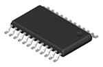
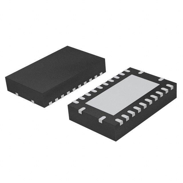
| 供应商器件封装 | 24-TSSOP |
| 其它名称 | 568-5114-2 |
| 包装 | 带卷 (TR) |
| 商标 | NXP Semiconductors |
| 安装类型 | 表面贴装 |
| 安装风格 | SMD/SMT |
| 封装 | Reel |
| 封装/外壳 | 24-TSSOP(0.173",4.40mm 宽) |
| 封装/箱体 | TSSOP-24 |
| 工作电源电压 | 4.5 V to 5.5 V |
| 工厂包装数量 | 2500 |
| 应用 | 自动 |
| 接口 | SPI 串行 |
| 最大工作温度 | + 125 C |
| 最小工作温度 | - 40 C |
| 标准包装 | 2,500 |
| 特色产品 | http://www.digikey.com/cn/zh/ph/NXP/I2C.html |
| 电压-电源 | 4.5 V ~ 5.5 V |
| 电源电压-最大 | 5.5 V |
| 电源电流 | 1 uA |
| 系列 | PCA9702 |


- 商务部:美国ITC正式对集成电路等产品启动337调查
- 曝三星4nm工艺存在良率问题 高通将骁龙8 Gen1或转产台积电
- 太阳诱电将投资9.5亿元在常州建新厂生产MLCC 预计2023年完工
- 英特尔发布欧洲新工厂建设计划 深化IDM 2.0 战略
- 台积电先进制程称霸业界 有大客户加持明年业绩稳了
- 达到5530亿美元!SIA预计今年全球半导体销售额将创下新高
- 英特尔拟将自动驾驶子公司Mobileye上市 估值或超500亿美元
- 三星加码芯片和SET,合并消费电子和移动部门,撤换高东真等 CEO
- 三星电子宣布重大人事变动 还合并消费电子和移动部门
- 海关总署:前11个月进口集成电路产品价值2.52万亿元 增长14.8%


PDF Datasheet 数据手册内容提取
PCA9703 18 V tolerant SPI 16-bit GPI with maskable INT Rev. 4 — 5 September 2014 Product data sheet 1. General description The PCA9703 is a low power 18V tolerant SPI General Purpose Input (GPI) shift register designed to monitor the status of switch inputs. It generates an interrupt when one or more of the switch inputs change state but allows selected inputs to not generate interrupts using the interrupt masking feature. The input level is recognized as a HIGH when it is greater than 0.8V and as a LOW when it is less than 0.55V (minimum DD DD LOW threshold of 2.5V at 5V node). The PCA9703 can monitor up to 16switch inputs. The falling edge of the CS pin samples the input port status and clears the interrupt. When CS is LOW, the rising edge of the SCLK loads the shift register and shifts the value out of the shift register. The serial input is sampled on the falling edge of SCLK. The contents of the shift register are loaded into the interrupt mask register of the device on the rising edge of CS. Each of the input ports has a 18V breakdown ESD protection circuit, which dumps the ESD/overvoltage current to ground. When used with a series resistor (minimum 100k), the input can connect to a 12V battery and support double battery, reverse battery, 27V jump start and 40V load dump conditions in automotive applications. Higher voltages can be tolerated on the inputs depending on the series resistor used to limit the input current. The INT_EN pin is used to both enable the GPI pins and to enable the INT output pin to minimize battery drain in cyclically supplied pull-up or pull-down applications. The SDIN pull-down prevents floating nodes when the device is used in daisy-chain applications. With both the high breakdown voltage and high ESD, this device is useful for both automotive (AEC-Q100 compliance available) and mobile applications. 2. Features and benefits 16 general purpose input ports 18V tolerant input ports with 100k external series resistor Input LOW threshold 0.55V with minimum of 2.5V at V =4.5V DD DD Open-drain interrupt output Interrupt enable pin (INT_EN) disables GPI pins and interrupt output Interrupt-masking feature allows no interrupt generation from selected inputs V range: 4.5V to 5.5V DD I is very low 2.5A maximum DD SPI serial interface with speeds up to 5MHz SPI supports daisy-chain connection for large switch numbers AEC-Q100 compliance available
PCA9703 NXP Semiconductors 18 V tolerant SPI 16-bit GPI with maskable INT ESD protection exceeds 5kV HBM per JESD22-A114 and 1000V CDM per JESD22-C101 Latch-up testing is done to JEDEC Standard JESD78 which exceeds 100mA Operating temperature range: 40Cto+125C Offered in TSSOP24 and HWQFN24 packages 3. Applications Automotive Body control modules Electronic control units (for example, for body controller) Switch monitoring SBC wake pin extension Industrial equipment Cellular telephones Emergency lighting 4. Ordering information Table 1. Ordering info rmation Type number Topside Package marking Name Description Version PCA9703HF 9703 HWQFN24 plastic thermal enhanced veryvery thin quad flat package; SOT994-1 noleads; 24 terminals; body 440.75mm PCA9703PW PCA9703PW TSSOP24 plastic thin shrink small outline package; 24leads; SOT355-1 bodywidth4.4mm PCA9703PW/Q900[1] PCA9703PW TSSOP24 plastic thin shrink small outline package; 24leads; SOT355-1 bodywidth4.4mm [1] PCA9703PW/Q900 is AEC-Q100 compliant. Contact i2c.support@nxp.com for PPAP. PCA9703 All information provided in this document is subject to legal disclaimers. © NXP B.V. 2014. All rights reserved. Product data sheet Rev. 4 — 5 September 2014 2 of 28
PCA9703 NXP Semiconductors 18 V tolerant SPI 16-bit GPI with maskable INT 5. Block diagram VDD INT PCA9703 INT_EN IN0 INPUT DFF0 R R E E T T S S IN1 INPUT DFF1 GI GI E E R R K T S F A HI M S SDOUT SDIN IN15 INPUT DFF15 SCLK INPUT CS STATUS REGISTER 20 μA VSS 002aae021 Fig 1. Block diagram of PCA9703 6. Pinning information 6.1 Pinning N T itnedrmexin aarle 1a INT_E INT SDOU VDD SDIN SCLK SDOIUNTT 12 2243 VSDDDIN 24 23 22 21 20 19 INT_EN 3 22 SCLK IN0 1 18 CS IN0 4 21 CS IN1 2 17 IN15 IN1 5 20 IN15 IN2 3 16 IN14 IN2 6 PCA9703PW 19 IN14 PCA9703HF IN3 4 15 IN13 IN3 7 PCA9703PW/Q900 18 IN13 IN4 5 14 IN12 IN4 8 17 IN12 IN5 6 13 IN11 IN5 9 16 IN11 7 8 9 10 11 12 IN6 10 15 IN10 IN7 11 14 IN9 6 7 S 8 9 0 IN IN VS IN IN N1 002aae024 VSS 12 13 IN8 I Transparent top view 002aae023 Fig 2. Pin configuration for HWQFN24 Fig 3. Pin configuration for TSSOP24 PCA9703 All information provided in this document is subject to legal disclaimers. © NXP B.V. 2014. All rights reserved. Product data sheet Rev. 4 — 5 September 2014 3 of 28
PCA9703 NXP Semiconductors 18 V tolerant SPI 16-bit GPI with maskable INT 6.2 Pin description Table 2. Pin description Symbol Pin Type Description TSSOP24 HWQFN24 SDOUT 1 22 output 3-state serial data output; normally high-impedance INT 2 23 output open-drain interrupt output (activeLOW) INT_EN 3 24 input GPI pin enable and interrupt output enable 1 = GPI pin and interrupt output are enabled 0 = GPI pin and interrupt output are disabled and interrupt output is high-impedance IN0 4 1 input input port0 IN1 5 2 input input port1 IN2 6 3 input input port2 IN3 7 4 input input port3 IN4 8 5 input input port4 IN5 9 6 input input port5 IN6 10 7 input input port6 IN7 11 8 input input port7 V 12 9[1] ground ground supply SS IN8 13 10 input input port8 IN9 14 11 input input port9 IN10 15 12 input input port10 IN11 16 13 input input port11 IN12 17 14 input input port12 IN13 18 15 input input port13 IN14 19 16 input input port14 IN15 20 17 input input port15 CS 21 18 input chip select (activeLOW) SCLK 22 19 input serial input clock SDIN 23 20 input serial data input (20A pull-down) V 24 21 supply supply voltage DD [1] HWQFN24 package die supply ground is connected to both V pin and exposed center pad. V pin must SS SS be connected to supply ground for proper device operation. For enhanced thermal, electrical, and board level performance, the exposed pad needs to be soldered to the board using a corresponding thermal pad on the board and for proper heat conduction through the board, thermal vias need to be incorporated in the PCB in the thermal pad region. PCA9703 All information provided in this document is subject to legal disclaimers. © NXP B.V. 2014. All rights reserved. Product data sheet Rev. 4 — 5 September 2014 4 of 28
PCA9703 NXP Semiconductors 18 V tolerant SPI 16-bit GPI with maskable INT 7. Functional description PCA9703 is a 16-bit General Purpose Input (GPI) with an open-drain interrupt output designed to monitor switch status. By putting an external 100k series resistor at the input port, the device allows the input to tolerate momentary double 12V battery, reverse battery, 27V jump start or 40V load dump conditions. The interrupt output is asserted when an input port status changes, the input is not masked and the interrupt output is enabled. The open-drain interrupt output is enabled when INT_EN is HIGH and disabled when INT_EN is LOW. The INT_EN also enables the GPI pins when it is HIGH. In cyclically supplied pull-up or pull-down applications, the GPI pull-ups or pull-downs should be active before the INT_EN is taken HIGH and the INT output should only be sampled after transient conditions have settled. Additionally, interrupts can be disabled in software by using the interrupt mask feature. The input port status is accessed via the 4-wire SPI interface. Upon power-up, the power-upreset cell clears all the registers, resulting in all zeros in both the input status register and the interrupt mask register. Since a zero in the interrupt mask register masks the interrupt from that pin, there will not be any interrupts generated. After power-up it is necessary to access the PCA9703 through the SPI pins in order to activate the interrupt for any GPI pins. When the PCA9703 is read over the SPI wires, the input conditions are clocked into the input status register on the CS falling edge. Since the inputs and the input status register now match, no interrupt is generated and any pre-existing interrupt is cleared. The input status register data is parallel loaded into the shift register on the first rising edge of the SCLK. The serial input data is captured on the opposite clock edge so that there is a 1⁄ clock cycle hold time. The set-up time is 2 diminished by the propagation time so the SCLK falling edge to rising edge must be long enough to provide sufficient set-up time. Successive clock cycles on the SCLK pin clock the data out of the PCA9703 and new data from the SDIN into the shift register. There is no limit to the number of clock cycles that can be applied with the CS LOW, however sufficient clock cycles should be used to both shift out all of the GPI data and shift in the new interrupt mask data to the correct position with the MSB first before the CS rising edge. For cyclic switch bias applications the switch bias should be applied first, then after the input voltage is settled the general purpose inputs are switched on by taking the INT_EN HIGH. This also enables the interrupt output, which will only indicate an interrupt if the GPI data does not match the input status register on a bit that is enabled by the interrupt mask register value. If an interrupt is generated, the pull-up or pull-down source should remain active and the INT_EN should remain active and the SPI pins are used to update the input status register and read the data out. They are also used to store the new interrupt mask on the rising edge of CS. After the SPI transaction is complete the INT_EN is taken LOW to turn the inputs off and disable the INT output. Then the GPI pull-ups or pull-downs can be turned off. The GPI pins are specifically designed so that any ESD/overstress current flows to ground, not V . They are also specifically designed so that if the input voltage DD returns to the same value after pull-up or pull-down bias cycling as before the input pull-up or pull-down bias cycling, before the input is enabled it will be detected as the same state. If the Input Status register is read when INT_EN is LOW, the input state at the INT_EN transition will be output regardless of the actual input levels since the GPI pins are turned off. PCA9703 All information provided in this document is subject to legal disclaimers. © NXP B.V. 2014. All rights reserved. Product data sheet Rev. 4 — 5 September 2014 5 of 28
PCA9703 NXP Semiconductors 18 V tolerant SPI 16-bit GPI with maskable INT If the V falls below the 4.5V minimum specified supply voltage, the input threshold will DD move down since they are a function of the V voltage. The input status register and the DD interrupt mask register retain their values to below V =2.0V and power-down can only DD be used to generate a power-up reset if the V falls below 0.2V before returning to the DD operating range. Multiple PCA9703 devices can be serially connected for monitoring a large number of switches by connecting the SDOUT of one device to the SDIN of the next device. SCLK and CS must be common among all devices and interrupt outputs may be tied together. No external logic is necessary because all the devices’ interrupt outputs are open-drain that function as ‘wired-AND’ and can simply be connected together to a single pull-up resistor. 7.1 SPI bus operation The PCA9703 interfaces with the controller via the 4-wire SPI bus that is comprised of the following signals: chip select (CS), serial clock (SCLK), serial data in (SDIN), and serial data out (SDOUT). To access the device, the controller asserts CS LOW, then sends SCLK and SDIN. When reading is complete and the interrupt mask data is in place, the controller de-asserts CS. See Figure4 for register access timing. 7.1.1 CS - chip select The CS pin is the device chip select and is an activeLOW input. The falling edge of CS captures the input port status in the input status register. If the interrupt output is asserted, the falling edge of CS will clear the interrupt. When CS is LOW, the SPI interface is active. When CS transitions HIGH the interrupt mask is stored and when CS is HIGH, the SPI interface is disabled. 7.1.2 SCLK - serial clock input SCLK is the serial clock input to the device. It should be LOW and remain LOW during the falling and rising edge of CS. When CS is LOW, the first rising edge of SCLK parallel loads the shift register from the input status register. The subsequent rising edges on SCLK serially shifts data out from the shift register. The falling edge of SCLK samples the data on SDIN. 7.1.3 SDIN - serial data input SDIN is the serial data input port. The data is sampled into the shift register on the falling edge of SCLK. SDIN is only active when CS is LOW. This input has a 20A pull-down current source to prevent the SDIN node from floating when CS is HIGH. 7.1.4 SDOUT - serial data output SDOUT is the serial data output signal. SDOUT is high-impedance when CS is HIGH and switches to low-impedance after CS goes LOW. When CS is LOW, after the first rising edge of SCLK the most significant bit in the shift register is presented on SDOUT. Subsequent rising edges of SCLK shift the remaining data from the shift register onto SDOUT. PCA9703 All information provided in this document is subject to legal disclaimers. © NXP B.V. 2014. All rights reserved. Product data sheet Rev. 4 — 5 September 2014 6 of 28
PCA9703 NXP Semiconductors 18 V tolerant SPI 16-bit GPI with maskable INT 7.1.5 Register access timing Figure4 shows the waveforms of the device operation. Initially CS is HIGH and SCLK is LOW. On the falling edge of CS, input port status, DATA[n:0] is captured into the input status register, and subsequently the first rising edge of SCLK parallel loads the shift register. The falling edge of SCLK samples the data on the SDIN. The MSB from the shift register is valid and available on the SDOUT after the first rising edge of SCLK. sample SDIN CS SCLK SDIN MSB in MSB − 1 in LSB in high-impedance SDOUT MSB out MSB − 1 out LSB out shift DATA[15:0] register input status DATA[15:0] register interrupt mask register 002aae286 DATA[15:0] is data on the input pins, IN[15:0]. Shaded areas indicate active but invalid data. Fig 4. Register access timing 7.1.6 Software reset operation Software reset will be activated by writing all zeroes into the shift register. This is identical to having an interrupt mask value of 0X00. Such an operation will reset the device, clear the input status register to zero and set the interrupt output to HIGH (no interrupt). 7.2 Interrupt output INT is the open-drain interrupt output and is activeLOW. A pull-up resistor of approximately 10k is recommended. A user-defined interrupt mask bit pattern is shifted into the shift register via SDIN. The value of bits in the mask pattern will determine which input pins will cause an interrupt. Any bit that is =0 will disable the input pin corresponding to that bit position from generating an interrupt. Interrupts will be enabled for bits having value =1. The mask bit pattern is not automatically aligned with the desired input pins. It is the responsibility of the programmer to shift the correct number of (mask) bits to the correct positions into the shift PCA9703 All information provided in this document is subject to legal disclaimers. © NXP B.V. 2014. All rights reserved. Product data sheet Rev. 4 — 5 September 2014 7 of 28
PCA9703 NXP Semiconductors 18 V tolerant SPI 16-bit GPI with maskable INT register. The interrupt mask bit pattern must be positioned into the shift register prior to the CS rising edge. Misaligned mask pattern will result in unexpected activation of the interrupt signal. The interrupt output is asserted when the input status is changed, and the interrupt mask bit corresponding to the input pin that caused the change is unmasked (bit value=1), and is cleared on the falling edge of CS or when the input port status matches the input status register. When there are multiple devices, the INT outputs may be tied together to a single pull-up. Table3 illustrates the state of the interrupt output versus the state of the input port and input status register. The interrupt output is asserted when the input port and input status register differ. Table 3. Interrupt output function truth table H=HIGH; L=LOW; X=don’t care INT_EN Input port status Input status register[1] INT output[2] Mask bit = 1 Mask bit = 0 (unmasked) (masked) H L L H H H L H L H H H L L H H H H H H L X X H H [1] Input status register is the value or content of the D flip-flops. [2] Logic states shown for INT pin assumes 10k pull-up resistor. 7.3 Interrupt enable INT_EN is the interrupt output enable input and the general purpose input enable input. It is an activeHIGH input. When the INT_EN pin is LOW the GPI pins are turned off and the input state is saved to minimize power loss when the input pull-ups or pull-downs are cycled and the INT output is disabled. The cycled pull-ups or pull-downs should be active sufficiently long before the INT_EN is taken active that the GPI pin voltage is completely settled to prevent false or transient interrupt signals. 7.4 General Purpose Inputs The General Purpose Inputs (GPI) are designed to behave like a typical input in the 0V to 5.5V range, but are also designed to have low leakage currents at elevated voltages. The input structure allows for elevated voltages to be applied through a series resistor. The series resistor is required when the input voltage is above 5.5V. The series resistor is required for two reasons: first, to prevent damage to the input avalanche diode, and second, to prevent the ESD protection circuitry from creating an excessive current flow. The ESD protection circuitry includes a latch-back style device, which provides excellent ESD protection during assembly or typical 5.5V applications. The series resistor limits the current flowing into the part and provides additional ESD protection. The limited current prevents the ESD latch-back device from latching back to a low voltage, which would cause excessive current flow and damage the part when the input voltage is above 5.5V. PCA9703 All information provided in this document is subject to legal disclaimers. © NXP B.V. 2014. All rights reserved. Product data sheet Rev. 4 — 5 September 2014 8 of 28
PCA9703 NXP Semiconductors 18 V tolerant SPI 16-bit GPI with maskable INT The minimum required series resistance for applications with input voltages above 5.5V is 100k. For applications requiring an applied voltage above 27V, Equation1 is recommended to determine the series resistor. Failure to include the appropriate input series resistor may result in product failure and will void the warranty. voltage applied–17 V R = ------------------------------------------------------------ (1) s I I The series resistor should be place physically as close as possible to the connected input to reduce the effective node capacitance. The input response time is effected by the RC time constant of the series resistor and the input node capacitance. 7.4.1 V , V and switching points IL IH A minimum LOW threshold of 2.5V is guaranteed for the logical switching points for the inputs. See Figure5 for details. VI HIGH VDD 0.8VDD VIH VIL hysteresis 0.55VDD minimum = 0.04VDD possible ground shift LOW 0 V 002aae101 Fig 5. Logic level thresholds The V is specified as a maximum of 0.55V and is 2.5V at 4.5VV . This means IL DD DD that if the user applies 2.5V or less to the input (with V =4.5V), or as the voltage DD passes this threshold, they will always see a LOW. The V is specified as a minimum of 0.8V . This means that if the user applies 3.6V IH DD or more to the input (with V =4.5V), or as the voltage passes this threshold, they will DD always see a HIGH. PCA9703 All information provided in this document is subject to legal disclaimers. © NXP B.V. 2014. All rights reserved. Product data sheet Rev. 4 — 5 September 2014 9 of 28
PCA9703 NXP Semiconductors 18 V tolerant SPI 16-bit GPI with maskable INT 8. Application design-in information 8.1 General application 4.5 V to 5.5 V 18 V 1.5 kΩ 100 kΩ IN0 VDD 10 kΩ relay INT CS CONTROLLER SCLK 18 V OR SDIN PROCESSOR SDOUT 100 kΩ IN1 INT_EN 180 V PCA9703 open 500 kΩ IN2 50 kΩ 5 V 10 kΩ IN15 VSS 002aae026 Fig 6. Typical application 8.2 Automotive application Supports: • 12V battery (8V to 16V) • Double battery (16V to 32V) • Reverse battery (8V to 16V) • Jump start (27V for 60seconds) • Load dump (40V) PCA9703 All information provided in this document is subject to legal disclaimers. © NXP B.V. 2014. All rights reserved. Product data sheet Rev. 4 — 5 September 2014 10 of 28
PCA9703 NXP Semiconductors 18 V tolerant SPI 16-bit GPI with maskable INT 8.2.1 SBC wake port extension with cyclic biasing System Basis Chips (SBC) offer many functions needed for in-vehicle networking solutions. Some of the features built into SBC are: • Transceivers (HS-CAN, LIN 2.0) • Scalable voltage regulators • Watchdog timers; wake-up function • Fail-safe function For more information on SBC, refer to www.nxp.com/products/interface_and_connectivity/system_basis_chips/. 8.2.1.1 UJA106x with PCA9703, standby V3 alternate PVR100AD-B5V0 UJA106x IN0 INT WAKE IN1 INT_EN V2 V1 GND PCA9703 VDD CS SDIN VCC IN15 SDOUT SCLK CSN VSS MOSI μC MISO SCLK GND 002aae027 Fig 7. UJA106x with PCA9703 with supplied microcontroller (standby) • PCA9703 fits to SBC UJA106x and UJA107xA family • PCA9703 can be powered by V1 of SBC • Extends the SBC with 16 additional wake inputs • C can be set to stop-mode during standby to save ECU standby current. SBC with GPI periodically monitors the wake inputs – Cyclic bias via V3 – Very low system current consumption even with clamped switches – Interrupt enable control via V2 PCA9703 All information provided in this document is subject to legal disclaimers. © NXP B.V. 2014. All rights reserved. Product data sheet Rev. 4 — 5 September 2014 11 of 28
PCA9703 NXP Semiconductors 18 V tolerant SPI 16-bit GPI with maskable INT 8.2.1.2 UJA107xA with PCA9703, standby and sleep alternate PDTA114E BAT 10 kΩ WBIAS V1 10 kΩ UJA107xA alternate 1 kΩ 1 kΩ 1 kΩ PDTA144E 47 kΩ WAKE1 47 kΩ WAKE2 VDD RSTN V1 GND PCA9703 10 kΩ 100 kΩ INT IN0 INT_EN 100 kΩ 10 kΩ IN1 CS VCC SDIN SDOUT CSN 100 kΩ IN15 VSS SCLK MOSI μC MISO SCLK GND 002aae029 Fig 8. UJA107xA with PCA9703 with supplied microcontroller (standby) alternate PDTA114E BAT 10 kΩ alternate 6.8 kΩ 10 kΩ WBIAS PVR100AD-B5V0 UJA107xA F alternate PDTA144E 1 kΩ 1 kΩ 1 kΩ n 70 47 kΩ WAKE1 4 47 kΩ WAKE2 VDD 10 kΩ RSTN PCA9703 10 kΩ alternate V1 GND PDTC144T 100 kΩ INT IN0 INT_EN 47 kΩ 100 kΩ 10 kΩ IN1 CS VCC SDIN SDOUT CSN 100 kΩ IN15 VSS SCLK MOSI μC MISO SCLK GND 002aae972 Fig 9. UJA107xA with PCA9703 with supplied microcontroller (sleep) • UJA107xA SBC provides WBIAS pin for cyclic biasing of the inputs • Compatible with UJA107xA based ASSPs PCA9703 All information provided in this document is subject to legal disclaimers. © NXP B.V. 2014. All rights reserved. Product data sheet Rev. 4 — 5 September 2014 12 of 28
PCA9703 NXP Semiconductors 18 V tolerant SPI 16-bit GPI with maskable INT 8.2.2 Application examples including switches to battery BAT BAT switch bias switch bias IN0 IN0 IN1 IN1 PCA9703 PCA9703 clamp 15 IN15 IN15 002aae030 002aae031 Fig 10. Clamp 15 (ignition) detection Fig 11. Switches to battery and ground with cyclicbiasing 9. Limiting values Table 4. Limiting valu es In accordance with the Absolute Maximum Rating System (IEC 60134). T =40Cto+125C, unless otherwise specified. amb Symbol Parameter Conditions Min Max Unit V supply voltage 0.5 +6.0 V DD I input current IN[15:0] pins with series resistor and [1] - 350 A I V >5.5V I V input voltage GPI pins IN[15:0]; no series resistor [1] 0.5 +6 V I SPI pins 0.5 +6 V T storage temperature 65 +150 C stg T maximum junction temperature operating - 125 C j(max) [1] With GPI external series resistors, the inputs support double battery, reverse battery and load dump conditions. During double battery or load dump the input pin will drain slightly higher leakage current until the input drops to 18V. For more detail of leakage current specification, please refer to Table 5 “Static characteristics”. See Section7.4 for series resistor requirements. PCA9703 All information provided in this document is subject to legal disclaimers. © NXP B.V. 2014. All rights reserved. Product data sheet Rev. 4 — 5 September 2014 13 of 28
PCA9703 NXP Semiconductors 18 V tolerant SPI 16-bit GPI with maskable INT 10. Static characteristics Table 5. Static charac teristics V =4.5V to 5.5V; V =0V; T =40Cto+125C; unless otherwise specified. DD SS amb Symbol Parameter Conditions Min Typ Max Unit Supply V supply voltage 4.5 5.0 5.5 V DD I supply current V =5.5V; input=5Vor18V; - 1.0 2.5 A DD DD INT_EN=V DD V power-on reset voltage [1] - 1.8 2.2 V POR General Purpose Inputs (IN0 to IN15) V LOW-level input voltage [2] - - 0.55V V IL DD V HIGH-level input voltage 0.8V - - V IH DD V hysteresis voltage V = 4.5 V - 70 - mV hys DD I input current GPI recommended maximum current; [3] - - 100 A I V >5.5V; with series resistor R I s I HIGH-level input current each input; V =V 1 - +1 A IH I DD I input leakage current V =17V; 100k series resistor 1 - +1 A LI I C input capacitance V =V orV - 2.0 5.0 pF i I SS DD Interrupt output (INT) I LOW-level output current V =4.5V; V =0.4V 6 - - mA OL DD OL I HIGH-level output current V =V 1 - +1 A OH OH DD C output capacitance - 2 5 pF o SPI and control (SDOUT, SDIN, SCLK, CS, INT_EN) V LOW-level input voltage - - 0.3V V IL DD V HIGH-level input voltage 0.7V - 5.5 V IH DD I HIGH-level input current SDIN; V =V =5.5V - 20 40 A IH I DD I LOW-level output current SDOUT; V =0.4V; V =4.5V 5 - - mA OL OL DD I HIGH-level output current SDOUT; V =V 0.5V; V =4.5V 5 11 - mA OH OH DD DD C input capacitance V =V orV - 2 5 pF i I SS DD C output capacitance SDOUT; CS=V - 4 6 pF o DD [1] VDD must be lowered to 0.2V for at least 5s in order to reset device. [2] Minimum V is 2.5V at V =4.5V. IL DD [3] For GPI pin voltages > 5.5V, see Section7.4. PCA9703 All information provided in this document is subject to legal disclaimers. © NXP B.V. 2014. All rights reserved. Product data sheet Rev. 4 — 5 September 2014 14 of 28
PCA9703 NXP Semiconductors 18 V tolerant SPI 16-bit GPI with maskable INT 11. Dynamic characteristics Table 6. Dynamic cha racteristics V =4.5V to 5.5V; V =0V; T =40Cto+125C; unless otherwise specified. DD SS amb Symbol Parameter Conditions Min Typ Max Unit f maximum input clock frequency - - 5 MHz max t rise time SDOUT; 10% to 90% at 5V - 35 60 ns r t fall time SDOUT; 90% to 10% at 5V - 25 50 ns f t pulse width HIGH SCLK 50 - - ns WH t pulse width LOW SCLK 50 - - ns WL t SPI enable lead time CS falling edge to SCLKrising edge 50 - - ns SPILEAD t SPI enable lag time SCLK falling edge to CSrising edge 50 - - ns SPILAG t SDIN set-up time SDIN to SCLKfallingedge 20 - - ns su(SDIN) t SDIN hold time from SCLK falling edge 30 - - ns h(SDIN) t SDOUT enable time from CS LOW to - - 55 ns en(SDOUT) SDOUTlow-impedance; Figure15 t SDOUT disable time from rising edge of CS to SDOUT - - 85 ns dis(SDOUT) high-impedance; Figure15 t SDOUT valid time from rising edge of SCLK; Figure16 - - 55 ns v(SDOUT) t SCLK set-up time SCLK falling to CS falling 50 - - ns su(SCLK) t SCLK hold time SCLK rising after CS rising 50 - - ns h(SCLK) t power-on reset pulse time time before CS is active - - 250 ns POR afterV >V DD POR t interrupt release time after CS going LOW; Figure17 - - 500 ns rel(int) t valid time on pin INT after INn changes or INT_EN - 200 800 ns v(INT) goesHIGH CS tsu(SCLK) tSPILEAD tWH tWL tSPILAG th(SCLK) SCLK 50 % 50 % tsu(SDIN) th(SDIN) SDIN MSB in ten(SDOUT) tv(SDOUT) tdis(SDOUT) high-impedance SDOUT MSB out trel(int) INT 002aac428 Fig 12. Timing diagram PCA9703 All information provided in this document is subject to legal disclaimers. © NXP B.V. 2014. All rights reserved. Product data sheet Rev. 4 — 5 September 2014 15 of 28
PCA9703 NXP Semiconductors 18 V tolerant SPI 16-bit GPI with maskable INT 2.5 V VDD VPOR 0 V CS SCLK SDOUT MSB out MSB − 1 tPOR 002aad158 Fig 13. AC waveform for t timing POR CS INn STATE 0 STATE 1 STATE 0 INT_EN tv(INT) tv(INT) INT trel(int) trel(int) 002aaf294 Fig 14. AC waveform for INT timing PCA9703 All information provided in this document is subject to legal disclaimers. © NXP B.V. 2014. All rights reserved. Product data sheet Rev. 4 — 5 September 2014 16 of 28
PCA9703 NXP Semiconductors 18 V tolerant SPI 16-bit GPI with maskable INT 12. Test information VDD open VDD RL 10 kΩ VI VO PULSE DUT GENERATOR RT C50L pF 10 kΩ 002aac580 Fig 15. Test circuitry for enable/disable times, SDOUT (t and t ) en(SDOUT) dis(SDOUT) VDD VI VO PULSE DUT GENERATOR RT C50L pF 002aac581 Fig 16. Test circuitry for switching times, SDOUT (t ) v(SDOUT) VDD VDD RL 10 kΩ VI VO PULSE DUT GENERATOR RT C50L pF 002aac582 Fig 17. Test circuitry for switching times, INT R =load resistance. L C =load capacitance includes jig and probe capacitance. L R =termination resistance should be equal to the output impedance Z of the pulse T o generators. PCA9703 All information provided in this document is subject to legal disclaimers. © NXP B.V. 2014. All rights reserved. Product data sheet Rev. 4 — 5 September 2014 17 of 28
PCA9703 NXP Semiconductors 18 V tolerant SPI 16-bit GPI with maskable INT 13. Package outline (cid:55)(cid:54)(cid:54)(cid:50)(cid:51)(cid:21)(cid:23)(cid:29)(cid:3)(cid:83)(cid:79)(cid:68)(cid:86)(cid:87)(cid:76)(cid:70)(cid:3)(cid:87)(cid:75)(cid:76)(cid:81)(cid:3)(cid:86)(cid:75)(cid:85)(cid:76)(cid:81)(cid:78)(cid:3)(cid:86)(cid:80)(cid:68)(cid:79)(cid:79)(cid:3)(cid:82)(cid:88)(cid:87)(cid:79)(cid:76)(cid:81)(cid:72)(cid:3)(cid:83)(cid:68)(cid:70)(cid:78)(cid:68)(cid:74)(cid:72)(cid:30)(cid:3)(cid:21)(cid:23)(cid:3)(cid:79)(cid:72)(cid:68)(cid:71)(cid:86)(cid:30)(cid:3)(cid:69)(cid:82)(cid:71)(cid:92)(cid:3)(cid:90)(cid:76)(cid:71)(cid:87)(cid:75)(cid:3)(cid:23)(cid:17)(cid:23)(cid:3)(cid:80)(cid:80)(cid:3) (cid:54)(cid:50)(cid:55)(cid:22)(cid:24)(cid:24)(cid:16)(cid:20)(cid:3) (cid:39)(cid:3) (cid:40)(cid:3) (cid:36)(cid:3) (cid:59)(cid:3) (cid:70)(cid:3) (cid:92)(cid:3) (cid:43)(cid:3)(cid:40)(cid:3) (cid:89)(cid:3)(cid:48)(cid:3) (cid:36)(cid:3) (cid:61)(cid:3) (cid:21)(cid:23)(cid:3) (cid:20)(cid:22)(cid:3) (cid:52)(cid:3) (cid:36)(cid:3)(cid:21)(cid:3) (cid:11)(cid:36)(cid:3)(cid:22)(cid:3)(cid:3)(cid:12)(cid:3) (cid:36)(cid:3) (cid:83)(cid:76)(cid:81)(cid:3)(cid:20)(cid:3)(cid:76)(cid:81)(cid:71)(cid:72)(cid:91)(cid:3) (cid:36)(cid:3)(cid:20)(cid:3) (cid:537)(cid:3) (cid:47)(cid:3)(cid:83)(cid:3) (cid:47)(cid:3) (cid:20)(cid:3) (cid:20)(cid:21)(cid:3) (cid:71)(cid:72)(cid:87)(cid:68)(cid:76)(cid:79)(cid:3)(cid:59)(cid:3) (cid:90)(cid:3)(cid:48)(cid:3) (cid:72)(cid:3) (cid:69)(cid:3)(cid:83)(cid:3) (cid:19)(cid:3) (cid:21)(cid:17)(cid:24)(cid:3) (cid:24)(cid:3)(cid:80)(cid:80)(cid:3) (cid:86)(cid:70)(cid:68)(cid:79)(cid:72)(cid:3) (cid:39)(cid:44)(cid:48)(cid:40)(cid:49)(cid:54)(cid:44)(cid:50)(cid:49)(cid:54)(cid:3)(cid:11)(cid:80)(cid:80)(cid:3)(cid:68)(cid:85)(cid:72)(cid:3)(cid:87)(cid:75)(cid:72)(cid:3)(cid:82)(cid:85)(cid:76)(cid:74)(cid:76)(cid:81)(cid:68)(cid:79)(cid:3)(cid:71)(cid:76)(cid:80)(cid:72)(cid:81)(cid:86)(cid:76)(cid:82)(cid:81)(cid:86)(cid:12)(cid:3)(cid:3) (cid:56)(cid:49)(cid:44)(cid:55)(cid:3) (cid:80)(cid:36)(cid:68)(cid:91)(cid:3)(cid:17)(cid:3) (cid:36)(cid:3)(cid:20)(cid:3) (cid:36)(cid:3)(cid:21)(cid:3) (cid:36)(cid:3)(cid:22)(cid:3) (cid:69)(cid:3)(cid:83)(cid:3) (cid:70)(cid:3) (cid:39)(cid:3)(cid:11)(cid:20)(cid:12)(cid:3) (cid:40)(cid:3)(cid:11)(cid:21)(cid:12)(cid:3) (cid:72)(cid:3) (cid:43)(cid:3)(cid:40)(cid:3) (cid:47)(cid:3) (cid:47)(cid:3)(cid:83)(cid:3) (cid:52)(cid:3) (cid:89)(cid:3) (cid:90)(cid:3) (cid:92)(cid:3) (cid:61)(cid:3)(cid:11)(cid:20)(cid:12)(cid:3) (cid:537)(cid:3) (cid:19)(cid:17)(cid:20)(cid:24)(cid:3) (cid:19)(cid:17)(cid:28)(cid:24)(cid:3) (cid:19)(cid:17)(cid:22)(cid:19)(cid:3) (cid:19)(cid:17)(cid:21)(cid:3) (cid:26)(cid:17)(cid:28)(cid:3) (cid:23)(cid:17)(cid:24)(cid:3) (cid:25)(cid:17)(cid:25)(cid:3) (cid:19)(cid:17)(cid:26)(cid:24)(cid:3) (cid:19)(cid:17)(cid:23)(cid:3) (cid:19)(cid:17)(cid:24)(cid:3) (cid:27)(cid:3)(cid:82)(cid:3) (cid:80)(cid:80)(cid:3) (cid:20)(cid:17)(cid:20)(cid:3) (cid:19)(cid:17)(cid:19)(cid:24)(cid:3) (cid:19)(cid:17)(cid:27)(cid:19)(cid:3) (cid:19)(cid:17)(cid:21)(cid:24)(cid:3) (cid:19)(cid:17)(cid:20)(cid:28)(cid:3) (cid:19)(cid:17)(cid:20)(cid:3) (cid:26)(cid:17)(cid:26)(cid:3) (cid:23)(cid:17)(cid:22)(cid:3) (cid:19)(cid:17)(cid:25)(cid:24)(cid:3) (cid:25)(cid:17)(cid:21)(cid:3) (cid:20)(cid:3) (cid:19)(cid:17)(cid:24)(cid:19)(cid:3) (cid:19)(cid:17)(cid:22)(cid:3) (cid:19)(cid:17)(cid:21)(cid:3) (cid:19)(cid:17)(cid:20)(cid:22)(cid:3) (cid:19)(cid:17)(cid:20)(cid:3) (cid:19)(cid:17)(cid:21)(cid:3) (cid:19)(cid:3)(cid:82)(cid:3) (cid:49)(cid:82)(cid:87)(cid:72)(cid:86)(cid:3) (cid:20)(cid:17)(cid:3)(cid:51)(cid:79)(cid:68)(cid:86)(cid:87)(cid:76)(cid:70)(cid:3)(cid:82)(cid:85)(cid:3)(cid:80)(cid:72)(cid:87)(cid:68)(cid:79)(cid:3)(cid:83)(cid:85)(cid:82)(cid:87)(cid:85)(cid:88)(cid:86)(cid:76)(cid:82)(cid:81)(cid:86)(cid:3)(cid:82)(cid:73)(cid:3)(cid:19)(cid:17)(cid:20)(cid:24)(cid:3)(cid:80)(cid:80)(cid:3)(cid:80)(cid:68)(cid:91)(cid:76)(cid:80)(cid:88)(cid:80)(cid:3)(cid:83)(cid:72)(cid:85)(cid:3)(cid:86)(cid:76)(cid:71)(cid:72)(cid:3)(cid:68)(cid:85)(cid:72)(cid:3)(cid:81)(cid:82)(cid:87)(cid:3)(cid:76)(cid:81)(cid:70)(cid:79)(cid:88)(cid:71)(cid:72)(cid:71)(cid:17)(cid:3) (cid:21)(cid:17)(cid:3)(cid:51)(cid:79)(cid:68)(cid:86)(cid:87)(cid:76)(cid:70)(cid:3)(cid:76)(cid:81)(cid:87)(cid:72)(cid:85)(cid:79)(cid:72)(cid:68)(cid:71)(cid:3)(cid:83)(cid:85)(cid:82)(cid:87)(cid:85)(cid:88)(cid:86)(cid:76)(cid:82)(cid:81)(cid:86)(cid:3)(cid:82)(cid:73)(cid:3)(cid:19)(cid:17)(cid:21)(cid:24)(cid:3)(cid:80)(cid:80)(cid:3)(cid:80)(cid:68)(cid:91)(cid:76)(cid:80)(cid:88)(cid:80)(cid:3)(cid:83)(cid:72)(cid:85)(cid:3)(cid:86)(cid:76)(cid:71)(cid:72)(cid:3)(cid:68)(cid:85)(cid:72)(cid:3)(cid:81)(cid:82)(cid:87)(cid:3)(cid:76)(cid:81)(cid:70)(cid:79)(cid:88)(cid:71)(cid:72)(cid:71)(cid:17)(cid:3) (cid:50)(cid:56)(cid:55)(cid:47)(cid:44)(cid:49)(cid:40)(cid:3) (cid:3)(cid:53)(cid:40)(cid:41)(cid:40)(cid:53)(cid:40)(cid:49)(cid:38)(cid:40)(cid:54)(cid:3) (cid:40)(cid:56)(cid:53)(cid:50)(cid:51)(cid:40)(cid:36)(cid:49)(cid:3) (cid:44)(cid:54)(cid:54)(cid:56)(cid:40)(cid:3)(cid:39)(cid:36)(cid:55)(cid:40)(cid:3) (cid:57)(cid:40)(cid:53)(cid:54)(cid:44)(cid:50)(cid:49)(cid:3) (cid:3)(cid:44)(cid:40)(cid:38)(cid:3) (cid:3)(cid:45)(cid:40)(cid:39)(cid:40)(cid:38)(cid:3) (cid:3)(cid:45)(cid:40)(cid:44)(cid:55)(cid:36)(cid:3) (cid:51)(cid:53)(cid:50)(cid:45)(cid:40)(cid:38)(cid:55)(cid:44)(cid:50)(cid:49)(cid:3) (cid:28)(cid:28)(cid:16)(cid:20)(cid:21)(cid:16)(cid:21)(cid:26)(cid:3) (cid:3)(cid:54)(cid:50)(cid:55)(cid:22)(cid:24)(cid:24)(cid:16)(cid:20)(cid:3) (cid:3)(cid:48)(cid:50)(cid:16)(cid:20)(cid:24)(cid:22)(cid:3) (cid:19)(cid:22)(cid:16)(cid:19)(cid:21)(cid:16)(cid:20)(cid:28)(cid:3) Fig 18. Package outline SOT355-1 (TSSOP24) PCA9703 All information provided in this document is subject to legal disclaimers. © NXP B.V. 2014. All rights reserved. Product data sheet Rev. 4 — 5 September 2014 18 of 28
PCA9703 NXP Semiconductors 18 V tolerant SPI 16-bit GPI with maskable INT (cid:43)(cid:58)(cid:52)(cid:41)(cid:49)(cid:21)(cid:23)(cid:29)(cid:3)(cid:83)(cid:79)(cid:68)(cid:86)(cid:87)(cid:76)(cid:70)(cid:3)(cid:87)(cid:75)(cid:72)(cid:85)(cid:80)(cid:68)(cid:79)(cid:3)(cid:72)(cid:81)(cid:75)(cid:68)(cid:81)(cid:70)(cid:72)(cid:71)(cid:3)(cid:89)(cid:72)(cid:85)(cid:92)(cid:3)(cid:89)(cid:72)(cid:85)(cid:92)(cid:3)(cid:87)(cid:75)(cid:76)(cid:81)(cid:3)(cid:84)(cid:88)(cid:68)(cid:71)(cid:3)(cid:73)(cid:79)(cid:68)(cid:87)(cid:3)(cid:83)(cid:68)(cid:70)(cid:78)(cid:68)(cid:74)(cid:72)(cid:30)(cid:3)(cid:81)(cid:82)(cid:3)(cid:79)(cid:72)(cid:68)(cid:71)(cid:86)(cid:30)(cid:3) (cid:21)(cid:23)(cid:3)(cid:87)(cid:72)(cid:85)(cid:80)(cid:76)(cid:81)(cid:68)(cid:79)(cid:86)(cid:30)(cid:3)(cid:69)(cid:82)(cid:71)(cid:92)(cid:3)(cid:23)(cid:3)(cid:91)(cid:3)(cid:23)(cid:3)(cid:91)(cid:3)(cid:19)(cid:17)(cid:26)(cid:24)(cid:3)(cid:80)(cid:80) (cid:54)(cid:50)(cid:55)(cid:28)(cid:28)(cid:23)(cid:16)(cid:20) (cid:39) (cid:37) (cid:36) (cid:87)(cid:72)(cid:85)(cid:80)(cid:76)(cid:81)(cid:68)(cid:79)(cid:3)(cid:20)(cid:3) (cid:76)(cid:81)(cid:71)(cid:72)(cid:91)(cid:3)(cid:68)(cid:85)(cid:72)(cid:68) (cid:40) (cid:36) (cid:36)(cid:20) (cid:70) (cid:71)(cid:72)(cid:87)(cid:68)(cid:76)(cid:79)(cid:3)(cid:59) (cid:72)(cid:20) (cid:20)(cid:18)(cid:21)(cid:3)(cid:72) (cid:38) (cid:0)(cid:3)(cid:89) (cid:48) (cid:38) (cid:36) (cid:37) (cid:72) (cid:69) (cid:0)(cid:3)(cid:90)(cid:48) (cid:38) (cid:92)(cid:20)(cid:38) (cid:92) (cid:26) (cid:20)(cid:21) (cid:47) (cid:20)(cid:22) (cid:25) (cid:72) (cid:40)(cid:75) (cid:72)(cid:21) (cid:20)(cid:18)(cid:21)(cid:3)(cid:72) (cid:20) (cid:20)(cid:27) (cid:87)(cid:72)(cid:85)(cid:80)(cid:76)(cid:81)(cid:68)(cid:79)(cid:3)(cid:20)(cid:3) (cid:76)(cid:81)(cid:71)(cid:72)(cid:91)(cid:3)(cid:68)(cid:85)(cid:72)(cid:68) (cid:21)(cid:23) (cid:20)(cid:28) (cid:59) (cid:39)(cid:75) (cid:19) (cid:21)(cid:17)(cid:24) (cid:24)(cid:3)(cid:80)(cid:80) (cid:86)(cid:70)(cid:68)(cid:79)(cid:72) (cid:39)(cid:44)(cid:48)(cid:40)(cid:49)(cid:54)(cid:44)(cid:50)(cid:49)(cid:54)(cid:3)(cid:11)(cid:80)(cid:80)(cid:3)(cid:68)(cid:85)(cid:72)(cid:3)(cid:87)(cid:75)(cid:72)(cid:3)(cid:82)(cid:85)(cid:76)(cid:74)(cid:76)(cid:81)(cid:68)(cid:79)(cid:3)(cid:71)(cid:76)(cid:80)(cid:72)(cid:81)(cid:86)(cid:76)(cid:82)(cid:81)(cid:86)(cid:12) (cid:56)(cid:49)(cid:44)(cid:55) (cid:80)(cid:36)(cid:11)(cid:68)(cid:20)(cid:91)(cid:12)(cid:3) (cid:36)(cid:20) (cid:69) (cid:70) (cid:39)(cid:11)(cid:20)(cid:12) (cid:39)(cid:75) (cid:40)(cid:11)(cid:20)(cid:12) (cid:40)(cid:75) (cid:72) (cid:72)(cid:20) (cid:72)(cid:21) (cid:47) (cid:89) (cid:90) (cid:92) (cid:92)(cid:20) (cid:19)(cid:17)(cid:19)(cid:24)(cid:3) (cid:19)(cid:17)(cid:22)(cid:19)(cid:3) (cid:23)(cid:17)(cid:20)(cid:3) (cid:21)(cid:17)(cid:21)(cid:24)(cid:3) (cid:23)(cid:17)(cid:20)(cid:3) (cid:21)(cid:17)(cid:21)(cid:24)(cid:3) (cid:19)(cid:17)(cid:24)(cid:3) (cid:80)(cid:80) (cid:19)(cid:17)(cid:27) (cid:19)(cid:17)(cid:21) (cid:19)(cid:17)(cid:24) (cid:21)(cid:17)(cid:24) (cid:21)(cid:17)(cid:24) (cid:19)(cid:17)(cid:20) (cid:19)(cid:17)(cid:19)(cid:24) (cid:19)(cid:17)(cid:19)(cid:24) (cid:19)(cid:17)(cid:20) (cid:19)(cid:17)(cid:19)(cid:19) (cid:19)(cid:17)(cid:20)(cid:27) (cid:22)(cid:17)(cid:28) (cid:20)(cid:17)(cid:28)(cid:24) (cid:22)(cid:17)(cid:28) (cid:20)(cid:17)(cid:28)(cid:24) (cid:19)(cid:17)(cid:22) (cid:49)(cid:82)(cid:87)(cid:72)(cid:3) (cid:20)(cid:17)(cid:3)(cid:51)(cid:79)(cid:68)(cid:86)(cid:87)(cid:76)(cid:70)(cid:3)(cid:82)(cid:85)(cid:3)(cid:80)(cid:72)(cid:87)(cid:68)(cid:79)(cid:3)(cid:83)(cid:85)(cid:82)(cid:87)(cid:85)(cid:88)(cid:86)(cid:76)(cid:82)(cid:81)(cid:86)(cid:3)(cid:82)(cid:73)(cid:3)(cid:19)(cid:17)(cid:19)(cid:26)(cid:24)(cid:3)(cid:80)(cid:80)(cid:3)(cid:80)(cid:68)(cid:91)(cid:76)(cid:80)(cid:88)(cid:80)(cid:3)(cid:83)(cid:72)(cid:85)(cid:3)(cid:86)(cid:76)(cid:71)(cid:72)(cid:3)(cid:68)(cid:85)(cid:72)(cid:3)(cid:81)(cid:82)(cid:87)(cid:3)(cid:76)(cid:81)(cid:70)(cid:79)(cid:88)(cid:71)(cid:72)(cid:71)(cid:17) (cid:50)(cid:56)(cid:55)(cid:47)(cid:44)(cid:49)(cid:40)(cid:3) (cid:53)(cid:40)(cid:41)(cid:40)(cid:53)(cid:40)(cid:49)(cid:38)(cid:40)(cid:54) (cid:40)(cid:56)(cid:53)(cid:50)(cid:51)(cid:40)(cid:36)(cid:49)(cid:3) (cid:44)(cid:54)(cid:54)(cid:56)(cid:40)(cid:3)(cid:39)(cid:36)(cid:55)(cid:40) (cid:57)(cid:40)(cid:53)(cid:54)(cid:44)(cid:50)(cid:49) (cid:44)(cid:40)(cid:38) (cid:45)(cid:40)(cid:39)(cid:40)(cid:38) (cid:45)(cid:40)(cid:44)(cid:55)(cid:36) (cid:51)(cid:53)(cid:50)(cid:45)(cid:40)(cid:38)(cid:55)(cid:44)(cid:50)(cid:49) (cid:19)(cid:26)(cid:16)(cid:19)(cid:21)(cid:16)(cid:19)(cid:26)(cid:3) (cid:54)(cid:50)(cid:55)(cid:28)(cid:28)(cid:23)(cid:16)(cid:20) (cid:16)(cid:3)(cid:16)(cid:3)(cid:16) (cid:48)(cid:50)(cid:16)(cid:21)(cid:21)(cid:19) (cid:16)(cid:3)(cid:16)(cid:3)(cid:16) (cid:19)(cid:26)(cid:16)(cid:19)(cid:22)(cid:16)(cid:19)(cid:22) Fig 19. Package outline SOT994-1 (HWQFN24) PCA9703 All information provided in this document is subject to legal disclaimers. © NXP B.V. 2014. All rights reserved. Product data sheet Rev. 4 — 5 September 2014 19 of 28
PCA9703 NXP Semiconductors 18 V tolerant SPI 16-bit GPI with maskable INT 14. Soldering of SMD packages This text provides a very brief insight into a complex technology. A more in-depth account of soldering ICs can be found in Application Note AN10365 “Surface mount reflow soldering description”. 14.1 Introduction to soldering Soldering is one of the most common methods through which packages are attached to Printed Circuit Boards (PCBs), to form electrical circuits. The soldered joint provides both the mechanical and the electrical connection. There is no single soldering method that is ideal for all IC packages. Wave soldering is often preferred when through-hole and Surface Mount Devices (SMDs) are mixed on one printed wiring board; however, it is not suitable for fine pitch SMDs. Reflow soldering is ideal for the small pitches and high densities that come with increased miniaturization. 14.2 Wave and reflow soldering Wave soldering is a joining technology in which the joints are made by solder coming from a standing wave of liquid solder. The wave soldering process is suitable for the following: • Through-hole components • Leaded or leadless SMDs, which are glued to the surface of the printed circuit board Not all SMDs can be wave soldered. Packages with solder balls, and some leadless packages which have solder lands underneath the body, cannot be wave soldered. Also, leaded SMDs with leads having a pitch smaller than ~0.6mm cannot be wave soldered, due to an increased probability of bridging. The reflow soldering process involves applying solder paste to a board, followed by component placement and exposure to a temperature profile. Leaded packages, packages with solder balls, and leadless packages are all reflow solderable. Key characteristics in both wave and reflow soldering are: • Board specifications, including the board finish, solder masks and vias • Package footprints, including solder thieves and orientation • The moisture sensitivity level of the packages • Package placement • Inspection and repair • Lead-free soldering versus SnPb soldering 14.3 Wave soldering Key characteristics in wave soldering are: • Process issues, such as application of adhesive and flux, clinching of leads, board transport, the solder wave parameters, and the time during which components are exposed to the wave • Solder bath specifications, including temperature and impurities PCA9703 All information provided in this document is subject to legal disclaimers. © NXP B.V. 2014. All rights reserved. Product data sheet Rev. 4 — 5 September 2014 20 of 28
PCA9703 NXP Semiconductors 18 V tolerant SPI 16-bit GPI with maskable INT 14.4 Reflow soldering Key characteristics in reflow soldering are: • Lead-free versus SnPb soldering; note that a lead-free reflow process usually leads to higher minimum peak temperatures (see Figure20) than a SnPb process, thus reducing the process window • Solder paste printing issues including smearing, release, and adjusting the process window for a mix of large and small components on one board • Reflow temperature profile; this profile includes preheat, reflow (in which the board is heated to the peak temperature) and cooling down. It is imperative that the peak temperature is high enough for the solder to make reliable solder joints (a solder paste characteristic). In addition, the peak temperature must be low enough that the packages and/or boards are not damaged. The peak temperature of the package depends on package thickness and volume and is classified in accordance with Table7 and8 Table 7. SnPb eutectic process (from J-STD-020D) Package thickness (mm) Package reflow temperature (C) Volume (mm3) < 350 350 < 2.5 235 220 2.5 220 220 Table 8. Lead-free process (from J-STD-020D) Package thickness (mm) Package reflow temperature (C) Volume (mm3) < 350 350 to 2000 > 2000 < 1.6 260 260 260 1.6 to 2.5 260 250 245 > 2.5 250 245 245 Moisture sensitivity precautions, as indicated on the packing, must be respected at all times. Studies have shown that small packages reach higher temperatures during reflow soldering, see Figure20. PCA9703 All information provided in this document is subject to legal disclaimers. © NXP B.V. 2014. All rights reserved. Product data sheet Rev. 4 — 5 September 2014 21 of 28
PCA9703 NXP Semiconductors 18 V tolerant SPI 16-bit GPI with maskable INT maximum peak temperature = MSL limit, damage level temperature minimum peak temperature = minimum soldering temperature peak temperature time 001aac844 MSL: Moisture Sensitivity Level Fig 20. Temperature profiles for large and small components For further information on temperature profiles, refer to Application Note AN10365 “Surface mount reflow soldering description”. PCA9703 All information provided in this document is subject to legal disclaimers. © NXP B.V. 2014. All rights reserved. Product data sheet Rev. 4 — 5 September 2014 22 of 28
PCA9703 NXP Semiconductors 18 V tolerant SPI 16-bit GPI with maskable INT 15. Soldering: PCB footprints (cid:41)(cid:82)(cid:82)(cid:87)(cid:83)(cid:85)(cid:76)(cid:81)(cid:87)(cid:3)(cid:76)(cid:81)(cid:73)(cid:82)(cid:85)(cid:80)(cid:68)(cid:87)(cid:76)(cid:82)(cid:81)(cid:3)(cid:73)(cid:82)(cid:85)(cid:3)(cid:85)(cid:72)(cid:73)(cid:79)(cid:82)(cid:90)(cid:3)(cid:86)(cid:82)(cid:79)(cid:71)(cid:72)(cid:85)(cid:76)(cid:81)(cid:74)(cid:3)(cid:82)(cid:73)(cid:3)(cid:55)(cid:54)(cid:54)(cid:50)(cid:51)(cid:21)(cid:23)(cid:3)(cid:83)(cid:68)(cid:70)(cid:78)(cid:68)(cid:74)(cid:72) (cid:54)(cid:50)(cid:55)(cid:22)(cid:24)(cid:24)(cid:16)(cid:20) (cid:43)(cid:91) (cid:42)(cid:91) (cid:51)(cid:21) (cid:11)(cid:19)(cid:17)(cid:20)(cid:21)(cid:24)(cid:12) (cid:11)(cid:19)(cid:17)(cid:20)(cid:21)(cid:24)(cid:12) (cid:43)(cid:92) (cid:42)(cid:92) (cid:37)(cid:92) (cid:36)(cid:92) (cid:38) (cid:39)(cid:21)(cid:3)(cid:11)(cid:23)(cid:91)(cid:12) (cid:51)(cid:20) (cid:39)(cid:20) (cid:42)(cid:72)(cid:81)(cid:72)(cid:85)(cid:76)(cid:70)(cid:3)(cid:73)(cid:82)(cid:82)(cid:87)(cid:83)(cid:85)(cid:76)(cid:81)(cid:87)(cid:3)(cid:83)(cid:68)(cid:87)(cid:87)(cid:72)(cid:85)(cid:81)(cid:3) (cid:53)(cid:72)(cid:73)(cid:72)(cid:85)(cid:3)(cid:87)(cid:82)(cid:3)(cid:87)(cid:75)(cid:72)(cid:3)(cid:83)(cid:68)(cid:70)(cid:78)(cid:68)(cid:74)(cid:72)(cid:3)(cid:82)(cid:88)(cid:87)(cid:79)(cid:76)(cid:81)(cid:72)(cid:3)(cid:71)(cid:85)(cid:68)(cid:90)(cid:76)(cid:81)(cid:74)(cid:3)(cid:73)(cid:82)(cid:85)(cid:3)(cid:68)(cid:70)(cid:87)(cid:88)(cid:68)(cid:79)(cid:3)(cid:79)(cid:68)(cid:92)(cid:82)(cid:88)(cid:87) (cid:86)(cid:82)(cid:79)(cid:71)(cid:72)(cid:85)(cid:3)(cid:79)(cid:68)(cid:81)(cid:71) (cid:82)(cid:70)(cid:70)(cid:88)(cid:83)(cid:76)(cid:72)(cid:71)(cid:3)(cid:68)(cid:85)(cid:72)(cid:68) (cid:39)(cid:44)(cid:48)(cid:40)(cid:49)(cid:54)(cid:44)(cid:50)(cid:49)(cid:54)(cid:3)(cid:76)(cid:81)(cid:3)(cid:80)(cid:80) (cid:51)(cid:20) (cid:51)(cid:21) (cid:36)(cid:92) (cid:37)(cid:92) (cid:38) (cid:39)(cid:20) (cid:39)(cid:21) (cid:42)(cid:91) (cid:42)(cid:92) (cid:43)(cid:91) (cid:43)(cid:92) (cid:19)(cid:17)(cid:25)(cid:24)(cid:19) (cid:19)(cid:17)(cid:26)(cid:24)(cid:19) (cid:26)(cid:17)(cid:21)(cid:19)(cid:19) (cid:23)(cid:17)(cid:24)(cid:19)(cid:19) (cid:20)(cid:17)(cid:22)(cid:24)(cid:19) (cid:19)(cid:17)(cid:23)(cid:19)(cid:19) (cid:19)(cid:17)(cid:25)(cid:19)(cid:19) (cid:27)(cid:17)(cid:21)(cid:19)(cid:19) (cid:24)(cid:17)(cid:22)(cid:19)(cid:19) (cid:27)(cid:17)(cid:25)(cid:19)(cid:19) (cid:26)(cid:17)(cid:23)(cid:24)(cid:19) (cid:86)(cid:82)(cid:87)(cid:22)(cid:24)(cid:24)(cid:16)(cid:20)(cid:66)(cid:73)(cid:85) Fig 21. PCB footprint for SOT355-1 (TSSOP24); reflow soldering PCA9703 All information provided in this document is subject to legal disclaimers. © NXP B.V. 2014. All rights reserved. Product data sheet Rev. 4 — 5 September 2014 23 of 28
PCA9703 NXP Semiconductors 18 V tolerant SPI 16-bit GPI with maskable INT (cid:41)(cid:82)(cid:82)(cid:87)(cid:83)(cid:85)(cid:76)(cid:81)(cid:87)(cid:3)(cid:76)(cid:81)(cid:73)(cid:82)(cid:85)(cid:80)(cid:68)(cid:87)(cid:76)(cid:82)(cid:81)(cid:3)(cid:73)(cid:82)(cid:85)(cid:3)(cid:85)(cid:72)(cid:73)(cid:79)(cid:82)(cid:90)(cid:3)(cid:86)(cid:82)(cid:79)(cid:71)(cid:72)(cid:85)(cid:76)(cid:81)(cid:74)(cid:3)(cid:82)(cid:73)(cid:3)(cid:43)(cid:57)(cid:52)(cid:41)(cid:49)(cid:21)(cid:23)(cid:3)(cid:83)(cid:68)(cid:70)(cid:78)(cid:68)(cid:74)(cid:72) (cid:54)(cid:50)(cid:55)(cid:28)(cid:28)(cid:23)(cid:16)(cid:20) (cid:43)(cid:91) (cid:42)(cid:91) (cid:39) (cid:51) (cid:19)(cid:17)(cid:19)(cid:21)(cid:24) (cid:19)(cid:17)(cid:19)(cid:21)(cid:24) (cid:38) (cid:11)(cid:19)(cid:17)(cid:20)(cid:19)(cid:24)(cid:12) (cid:54)(cid:51)(cid:91) (cid:81)(cid:54)(cid:51)(cid:91) (cid:54)(cid:51)(cid:92) (cid:82)(cid:87) (cid:43)(cid:92) (cid:42)(cid:92) (cid:92)(cid:3)(cid:87) (cid:54)(cid:47)(cid:92) (cid:37)(cid:92) (cid:36)(cid:92) (cid:51) (cid:81)(cid:54)(cid:51)(cid:92) (cid:54) (cid:54)(cid:51)(cid:91)(cid:3)(cid:87)(cid:82)(cid:87) (cid:54)(cid:47)(cid:91) (cid:37)(cid:91) (cid:36)(cid:91) (cid:42)(cid:72)(cid:81)(cid:72)(cid:85)(cid:76)(cid:70)(cid:3)(cid:73)(cid:82)(cid:82)(cid:87)(cid:83)(cid:85)(cid:76)(cid:81)(cid:87)(cid:3)(cid:83)(cid:68)(cid:87)(cid:87)(cid:72)(cid:85)(cid:81)(cid:3) (cid:53)(cid:72)(cid:73)(cid:72)(cid:85)(cid:3)(cid:87)(cid:82)(cid:3)(cid:87)(cid:75)(cid:72)(cid:3)(cid:83)(cid:68)(cid:70)(cid:78)(cid:68)(cid:74)(cid:72)(cid:3)(cid:82)(cid:88)(cid:87)(cid:79)(cid:76)(cid:81)(cid:72)(cid:3)(cid:71)(cid:85)(cid:68)(cid:90)(cid:76)(cid:81)(cid:74)(cid:3)(cid:73)(cid:82)(cid:85)(cid:3)(cid:68)(cid:70)(cid:87)(cid:88)(cid:68)(cid:79)(cid:3)(cid:79)(cid:68)(cid:92)(cid:82)(cid:88)(cid:87) (cid:86)(cid:82)(cid:79)(cid:71)(cid:72)(cid:85)(cid:3)(cid:79)(cid:68)(cid:81)(cid:71) (cid:86)(cid:82)(cid:79)(cid:71)(cid:72)(cid:85)(cid:3)(cid:83)(cid:68)(cid:86)(cid:87)(cid:72)(cid:3)(cid:71)(cid:72)(cid:83)(cid:82)(cid:86)(cid:76)(cid:87) (cid:86)(cid:82)(cid:79)(cid:71)(cid:72)(cid:85)(cid:3)(cid:79)(cid:68)(cid:81)(cid:71)(cid:3)(cid:83)(cid:79)(cid:88)(cid:86)(cid:3)(cid:86)(cid:82)(cid:79)(cid:71)(cid:72)(cid:85)(cid:3)(cid:83)(cid:68)(cid:86)(cid:87)(cid:72) (cid:82)(cid:70)(cid:70)(cid:88)(cid:83)(cid:76)(cid:72)(cid:71)(cid:3)(cid:68)(cid:85)(cid:72)(cid:68) (cid:81)(cid:54)(cid:51)(cid:91) (cid:81)(cid:54)(cid:51)(cid:92) (cid:21) (cid:21) (cid:39)(cid:76)(cid:80)(cid:72)(cid:81)(cid:86)(cid:76)(cid:82)(cid:81)(cid:86)(cid:3)(cid:76)(cid:81)(cid:3)(cid:80)(cid:80) (cid:51) (cid:36)(cid:91) (cid:36)(cid:92) (cid:37)(cid:91) (cid:37)(cid:92) (cid:38) (cid:39) (cid:54)(cid:47)(cid:91) (cid:54)(cid:47)(cid:92) (cid:54)(cid:51)(cid:91)(cid:3)(cid:87)(cid:82)(cid:87) (cid:54)(cid:51)(cid:92)(cid:3)(cid:87)(cid:82)(cid:87) (cid:54)(cid:51)(cid:91) (cid:54)(cid:51)(cid:92) (cid:42)(cid:91) (cid:42)(cid:92) (cid:43)(cid:91) (cid:43)(cid:92) (cid:19)(cid:17)(cid:24)(cid:19)(cid:19) (cid:24)(cid:17)(cid:19)(cid:19)(cid:19) (cid:24)(cid:17)(cid:19)(cid:19)(cid:19) (cid:22)(cid:17)(cid:21)(cid:19)(cid:19) (cid:22)(cid:17)(cid:21)(cid:19)(cid:19) (cid:19)(cid:17)(cid:28)(cid:19)(cid:19) (cid:19)(cid:17)(cid:21)(cid:23)(cid:19) (cid:21)(cid:17)(cid:20)(cid:19)(cid:19) (cid:21)(cid:17)(cid:20)(cid:19)(cid:19) (cid:20)(cid:17)(cid:21)(cid:19)(cid:19) (cid:20)(cid:17)(cid:21)(cid:19)(cid:19) (cid:19)(cid:17)(cid:23)(cid:24)(cid:19) (cid:19)(cid:17)(cid:23)(cid:24)(cid:19) (cid:23)(cid:17)(cid:22)(cid:19)(cid:19) (cid:23)(cid:17)(cid:22)(cid:19)(cid:19) (cid:24)(cid:17)(cid:21)(cid:24)(cid:19) (cid:24)(cid:17)(cid:21)(cid:24)(cid:19) (cid:19)(cid:26)(cid:16)(cid:19)(cid:28)(cid:16)(cid:21)(cid:23)(cid:3) (cid:44)(cid:86)(cid:86)(cid:88)(cid:72)(cid:3)(cid:71)(cid:68)(cid:87)(cid:72) (cid:86)(cid:82)(cid:87)(cid:28)(cid:28)(cid:23)(cid:16)(cid:20)(cid:66)(cid:73)(cid:85) (cid:19)(cid:28)(cid:16)(cid:19)(cid:25)(cid:16)(cid:20)(cid:24) Fig 22. PCB footprint for SOT994-1 (HWQFN24); reflow soldering PCA9703 All information provided in this document is subject to legal disclaimers. © NXP B.V. 2014. All rights reserved. Product data sheet Rev. 4 — 5 September 2014 24 of 28
PCA9703 NXP Semiconductors 18 V tolerant SPI 16-bit GPI with maskable INT 16. Abbreviations Table 9. Abbreviations Acronym Description ASSP Application Specific Standard Product CAN Controller Area Network CDM Charged-Device Model DUT Device Under Test ECU Electronic Control Unit ESD ElectroStatic Discharge GPI General Purpose Input HBM Human Body Model HS-CAN High-Speed Controller Area Network LIN Local Interconnect Network MSB Most Significant Bit PCB Printed-Circuit Board PPAP Production Part Approval Process RC Resistor-Capacitor network SBC System Basis Chip SPI Serial Peripheral Interface C microcontroller 17. Revision history Table 10. Revision history Document ID Release date Data sheet status Change notice Supersedes PCA9703 v.4 20140905 Product data sheet - PCA9703 v.3 Modifications: • Table5, V : Updated conditions, min, typ and unit. Removed table note [3]. Aligned to hys characterization data, no change to device. • Removed references to hysteresis in Section2, Figure5, Section7.4.1. PCA9703 v.3 20140317 Product data sheet - PCA9703 v.2 PCA9703 v.2 20120614 Product data sheet - PCA9703 v.1 PCA9703 v.1 20100223 Product data sheet - - PCA9703 All information provided in this document is subject to legal disclaimers. © NXP B.V. 2014. All rights reserved. Product data sheet Rev. 4 — 5 September 2014 25 of 28
PCA9703 NXP Semiconductors 18 V tolerant SPI 16-bit GPI with maskable INT 18. Legal information 18.1 Data sheet status Document status[1][2] Product status[3] Definition Objective [short] data sheet Development This document contains data from the objective specification for product development. Preliminary [short] data sheet Qualification This document contains data from the preliminary specification. Product [short] data sheet Production This document contains the product specification. [1] Please consult the most recently issued document before initiating or completing a design. [2] The term ‘short data sheet’ is explained in section “Definitions”. [3] The product status of device(s) described in this document may have changed since this document was published and may differ in case of multiple devices. The latest product status information is available on the Internet at URLhttp://www.nxp.com. 18.2 Definitions Suitability for use in automotive applications — This NXP Semiconductors product has been qualified for use in automotive applications. Unless otherwise agreed in writing, the product is not designed, Draft — The document is a draft version only. The content is still under authorized or warranted to be suitable for use in life support, life-critical or internal review and subject to formal approval, which may result in safety-critical systems or equipment, nor in applications where failure or modifications or additions. NXP Semiconductors does not give any malfunction of an NXP Semiconductors product can reasonably be expected representations or warranties as to the accuracy or completeness of to result in personal injury, death or severe property or environmental information included herein and shall have no liability for the consequences of damage. NXP Semiconductors and its suppliers accept no liability for use of such information. inclusion and/or use of NXP Semiconductors products in such equipment or Short data sheet — A short data sheet is an extract from a full data sheet applications and therefore such inclusion and/or use is at the customer's own with the same product type number(s) and title. A short data sheet is intended risk. for quick reference only and should not be relied upon to contain detailed and Applications — Applications that are described herein for any of these full information. For detailed and full information see the relevant full data products are for illustrative purposes only. NXP Semiconductors makes no sheet, which is available on request via the local NXP Semiconductors sales representation or warranty that such applications will be suitable for the office. In case of any inconsistency or conflict with the short data sheet, the specified use without further testing or modification. full data sheet shall prevail. Customers are responsible for the design and operation of their applications Product specification — The information and data provided in a Product and products using NXP Semiconductors products, and NXP Semiconductors data sheet shall define the specification of the product as agreed between accepts no liability for any assistance with applications or customer product NXP Semiconductors and its customer, unless NXP Semiconductors and design. It is customer’s sole responsibility to determine whether the NXP customer have explicitly agreed otherwise in writing. In no event however, Semiconductors product is suitable and fit for the customer’s applications and shall an agreement be valid in which the NXP Semiconductors product is products planned, as well as for the planned application and use of deemed to offer functions and qualities beyond those described in the customer’s third party customer(s). Customers should provide appropriate Product data sheet. design and operating safeguards to minimize the risks associated with their applications and products. 18.3 Disclaimers NXP Semiconductors does not accept any liability related to any default, damage, costs or problem which is based on any weakness or default in the customer’s applications or products, or the application or use by customer’s Limited warranty and liability — Information in this document is believed to third party customer(s). Customer is responsible for doing all necessary be accurate and reliable. However, NXP Semiconductors does not give any testing for the customer’s applications and products using NXP representations or warranties, expressed or implied, as to the accuracy or Semiconductors products in order to avoid a default of the applications and completeness of such information and shall have no liability for the the products or of the application or use by customer’s third party consequences of use of such information. NXP Semiconductors takes no customer(s). NXP does not accept any liability in this respect. responsibility for the content in this document if provided by an information source outside of NXP Semiconductors. Limiting values — Stress above one or more limiting values (as defined in the Absolute Maximum Ratings System of IEC60134) will cause permanent In no event shall NXP Semiconductors be liable for any indirect, incidental, damage to the device. Limiting values are stress ratings only and (proper) punitive, special or consequential damages (including - without limitation - lost operation of the device at these or any other conditions above those given in profits, lost savings, business interruption, costs related to the removal or the Recommended operating conditions section (if present) or the replacement of any products or rework charges) whether or not such Characteristics sections of this document is not warranted. Constant or damages are based on tort (including negligence), warranty, breach of repeated exposure to limiting values will permanently and irreversibly affect contract or any other legal theory. the quality and reliability of the device. Notwithstanding any damages that customer might incur for any reason Terms and conditions of commercial sale — NXP Semiconductors whatsoever, NXP Semiconductors’ aggregate and cumulative liability towards products are sold subject to the general terms and conditions of commercial customer for the products described herein shall be limited in accordance with the Terms and conditions of commercial sale of NXP Semiconductors. sale, as published at http://www.nxp.com/profile/terms, unless otherwise agreed in a valid written individual agreement. In case an individual Right to make changes — NXP Semiconductors reserves the right to make agreement is concluded only the terms and conditions of the respective changes to information published in this document, including without agreement shall apply. NXP Semiconductors hereby expressly objects to limitation specifications and product descriptions, at any time and without applying the customer’s general terms and conditions with regard to the notice. This document supersedes and replaces all information supplied prior purchase of NXP Semiconductors products by customer. to the publication hereof. PCA9703 All information provided in this document is subject to legal disclaimers. © NXP B.V. 2014. All rights reserved. Product data sheet Rev. 4 — 5 September 2014 26 of 28
PCA9703 NXP Semiconductors 18 V tolerant SPI 16-bit GPI with maskable INT No offer to sell or license — Nothing in this document may be interpreted or Translations — A non-English (translated) version of a document is for construed as an offer to sell products that is open for acceptance or the grant, reference only. The English version shall prevail in case of any discrepancy conveyance or implication of any license under any copyrights, patents or between the translated and English versions. other industrial or intellectual property rights. Export control — This document as well as the item(s) described herein 18.4 Trademarks may be subject to export control regulations. Export might require a prior authorization from competent authorities. Notice: All referenced brands, product names, service names and trademarks are the property of their respective owners. 19. Contact information For more information, please visit: http://www.nxp.com For sales office addresses, please send an email to: salesaddresses@nxp.com PCA9703 All information provided in this document is subject to legal disclaimers. © NXP B.V. 2014. All rights reserved. Product data sheet Rev. 4 — 5 September 2014 27 of 28
PCA9703 NXP Semiconductors 18 V tolerant SPI 16-bit GPI with maskable INT 20. Contents 1 General description. . . . . . . . . . . . . . . . . . . . . . 1 18.3 Disclaimers . . . . . . . . . . . . . . . . . . . . . . . . . . 26 2 Features and benefits . . . . . . . . . . . . . . . . . . . . 1 18.4 Trademarks . . . . . . . . . . . . . . . . . . . . . . . . . . 27 3 Applications. . . . . . . . . . . . . . . . . . . . . . . . . . . . 2 19 Contact information . . . . . . . . . . . . . . . . . . . . 27 4 Ordering information. . . . . . . . . . . . . . . . . . . . . 2 20 Contents. . . . . . . . . . . . . . . . . . . . . . . . . . . . . . 28 5 Block diagram . . . . . . . . . . . . . . . . . . . . . . . . . . 3 6 Pinning information. . . . . . . . . . . . . . . . . . . . . . 3 6.1 Pinning . . . . . . . . . . . . . . . . . . . . . . . . . . . . . . . 3 6.2 Pin description . . . . . . . . . . . . . . . . . . . . . . . . . 4 7 Functional description . . . . . . . . . . . . . . . . . . . 5 7.1 SPI bus operation. . . . . . . . . . . . . . . . . . . . . . . 6 7.1.1 CS - chip select . . . . . . . . . . . . . . . . . . . . . . . . 6 7.1.2 SCLK - serial clock input . . . . . . . . . . . . . . . . . 6 7.1.3 SDIN - serial data input. . . . . . . . . . . . . . . . . . . 6 7.1.4 SDOUT - serial data output . . . . . . . . . . . . . . . 6 7.1.5 Register access timing. . . . . . . . . . . . . . . . . . . 7 7.1.6 Software reset operation. . . . . . . . . . . . . . . . . . 7 7.2 Interrupt output. . . . . . . . . . . . . . . . . . . . . . . . . 7 7.3 Interrupt enable . . . . . . . . . . . . . . . . . . . . . . . . 8 7.4 General Purpose Inputs . . . . . . . . . . . . . . . . . . 8 7.4.1 V , V and switching points. . . . . . . . . . . . . . . 9 IL IH 8 Application design-in information . . . . . . . . . 10 8.1 General application. . . . . . . . . . . . . . . . . . . . . 10 8.2 Automotive application. . . . . . . . . . . . . . . . . . 10 8.2.1 SBC wake port extension with cyclic biasing . 11 8.2.1.1 UJA106x with PCA9703, standby. . . . . . . . . . 11 8.2.1.2 UJA107xA with PCA9703, standby and sleep 12 8.2.2 Application examples including switches to battery. . . . . . . . . . . . . . . . . . . . . . . . . . . . . . . 13 9 Limiting values. . . . . . . . . . . . . . . . . . . . . . . . . 13 10 Static characteristics. . . . . . . . . . . . . . . . . . . . 14 11 Dynamic characteristics. . . . . . . . . . . . . . . . . 15 12 Test information. . . . . . . . . . . . . . . . . . . . . . . . 17 13 Package outline. . . . . . . . . . . . . . . . . . . . . . . . 18 14 Soldering of SMD packages . . . . . . . . . . . . . . 20 14.1 Introduction to soldering. . . . . . . . . . . . . . . . . 20 14.2 Wave and reflow soldering. . . . . . . . . . . . . . . 20 14.3 Wave soldering. . . . . . . . . . . . . . . . . . . . . . . . 20 14.4 Reflow soldering. . . . . . . . . . . . . . . . . . . . . . . 21 15 Soldering: PCB footprints. . . . . . . . . . . . . . . . 23 16 Abbreviations. . . . . . . . . . . . . . . . . . . . . . . . . . 25 17 Revision history. . . . . . . . . . . . . . . . . . . . . . . . 25 18 Legal information. . . . . . . . . . . . . . . . . . . . . . . 26 18.1 Data sheet status . . . . . . . . . . . . . . . . . . . . . . 26 18.2 Definitions. . . . . . . . . . . . . . . . . . . . . . . . . . . . 26 Please be aware that important notices concerning this document and the product(s) described herein, have been included in section ‘Legal information’. © NXP B.V. 2014. All rights reserved. For more information, please visit: http://www.nxp.com For sales office addresses, please send an email to: salesaddresses@nxp.com Date of release: 5 September 2014 Document identifier: PCA9703
Mouser Electronics Authorized Distributor Click to View Pricing, Inventory, Delivery & Lifecycle Information: N XP: PCA9703PW,112 PCA9703PW,118 PCA9703PW/Q900,118