ICGOO在线商城 > 集成电路(IC) > 嵌入式 - CPLD(复杂可编程逻辑器件) > XC9536XL-10VQG64C
 Datasheet下载
- 型号: XC9536XL-10VQG64C
- 制造商: Xilinx
- 库位|库存: xxxx|xxxx
- 要求:
| 数量阶梯 | 香港交货 | 国内含税 |
| +xxxx | $xxxx | ¥xxxx |
查看当月历史价格
查看今年历史价格
XC9536XL-10VQG64C产品简介:
ICGOO电子元器件商城为您提供XC9536XL-10VQG64C由Xilinx设计生产,在icgoo商城现货销售,并且可以通过原厂、代理商等渠道进行代购。 XC9536XL-10VQG64C价格参考。XilinxXC9536XL-10VQG64C封装/规格:嵌入式 - CPLD(复杂可编程逻辑器件), 。您可以下载XC9536XL-10VQG64C参考资料、Datasheet数据手册功能说明书,资料中有XC9536XL-10VQG64C 详细功能的应用电路图电压和使用方法及教程。
Xilinx Inc. 的 XC9536XL-10VQG64C 是一款复杂可编程逻辑器件(CPLD),属于嵌入式系统中的重要组成部分。它具有高集成度、低功耗和灵活性等特点,适用于多种应用场景。

 1. 工业控制
在工业自动化领域,XC9536XL-10VQG64C 可用于实现复杂的控制逻辑。例如,在PLC(可编程逻辑控制器)中,它可以处理传感器输入、执行逻辑运算并输出控制信号,确保生产设备的高效运行。其低功耗特性使其适合长时间稳定工作,减少维护成本。

 2. 通信设备
通信系统中,XC9536XL-10VQG64C 可以用于协议转换、信号处理等任务。它能够快速响应外部信号变化,提供实时数据处理能力,适用于网络接口卡、路由器和交换机等设备。此外,其灵活的配置能力使得它可以适应不同通信标准的变化需求。

 3. 消费电子
在消费电子产品中,XC9536XL-10VQG64C 可用于实现各种功能模块的接口桥接。例如,在智能家居设备中,它可以连接不同的传感器和执行器,实现智能化控制。其小尺寸封装(VQG64)使得它非常适合应用于空间有限的便携式设备中。

 4. 汽车电子
汽车电子系统中,XC9536XL-10VQG64C 可用于车身控制模块(BCM)、发动机控制单元(ECU)等关键部件。它能够处理多个传感器输入,并根据预设逻辑输出控制信号,确保车辆的安全性和可靠性。此外,其抗干扰能力强,能够在恶劣的电磁环境中稳定工作。

 5. 医疗设备
医疗设备对可靠性和安全性要求极高,XC9536XL-10VQG64C 在此领域也有广泛应用。它可以用于生命体征监测仪、监护设备等,处理来自传感器的数据,进行实时分析和报警。其低功耗和高稳定性使得它能够在电池供电的情况下长时间工作,确保患者的安全。

总之,XC9536XL-10VQG64C 凭借其高性能、低功耗和灵活性,广泛应用于工业控制、通信设备、消费电子、汽车电子和医疗设备等多个领域,为各种嵌入式系统提供了可靠的解决方案。
| 参数 | 数值 |
| 产品目录 | 集成电路 (IC) |
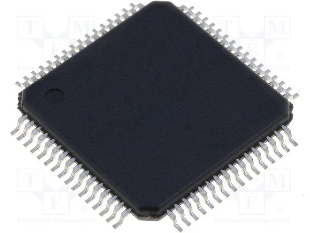
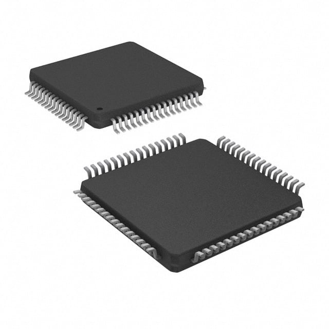
| 描述 | IC CPLD 36MC 10NS 64VQFP |
| 产品分类 | |
| I/O数 | 36 |
| 品牌 | Xilinx Inc |
| 数据手册 | |
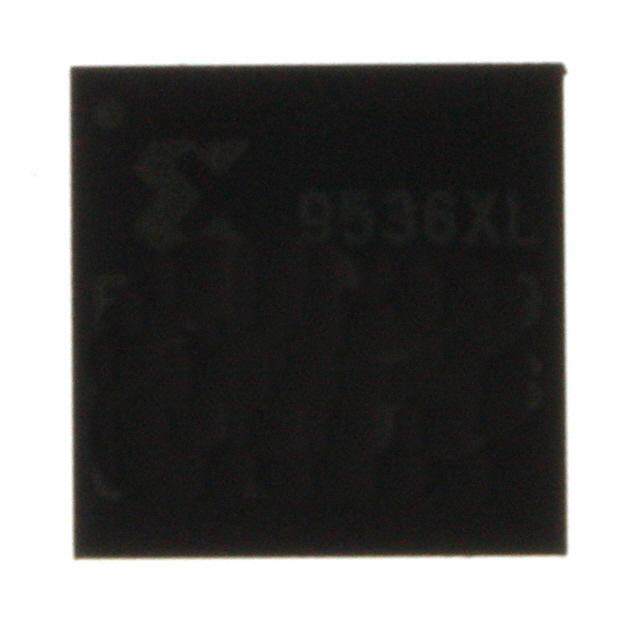
| 产品图片 |
|
| 产品型号 | XC9536XL-10VQG64C |
| rohs | 无铅 / 符合限制有害物质指令(RoHS)规范要求 |
| 产品系列 | XC9500XL |
| 产品目录页面 | |
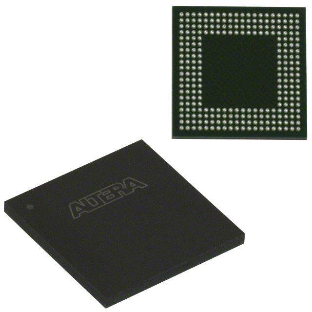
| 供应商器件封装 | 64-VQFP(10x10) |
| 其它名称 | 122-1435 |
| 包装 | 托盘 |
| 可编程类型 | 系统内可编程(最少 10,000 次编程/擦除循环) |
| 安装类型 | 表面贴装 |
| 宏单元数 | 36 |
| 封装/外壳 | 64-TQFP |
| 工作温度 | 0°C ~ 70°C |
| 延迟时间tpd(1)最大值 | 10.0ns |
| 栅极数 | 800 |
| 标准包装 | 160 |
| 电源电压-内部 | 3 V ~ 3.6 V |
| 逻辑元件/块数 | 2 |


- 商务部:美国ITC正式对集成电路等产品启动337调查
- 曝三星4nm工艺存在良率问题 高通将骁龙8 Gen1或转产台积电
- 太阳诱电将投资9.5亿元在常州建新厂生产MLCC 预计2023年完工
- 英特尔发布欧洲新工厂建设计划 深化IDM 2.0 战略
- 台积电先进制程称霸业界 有大客户加持明年业绩稳了
- 达到5530亿美元!SIA预计今年全球半导体销售额将创下新高
- 英特尔拟将自动驾驶子公司Mobileye上市 估值或超500亿美元
- 三星加码芯片和SET,合并消费电子和移动部门,撤换高东真等 CEO
- 三星电子宣布重大人事变动 还合并消费电子和移动部门
- 海关总署:前11个月进口集成电路产品价值2.52万亿元 增长14.8%

PDF Datasheet 数据手册内容提取
0 XC9536XL High Performance R CPLD DS058 (v1.9) April 3, 2007 Product Specification 0 0 Features 54V18 Function Blocks, providing 800 usable gates with propagation delays of 5ns. See Figure2 for architecture • 5 ns pin-to-pin logic delays • System frequency up to 178 MHz overview. • 36 macrocells with 800 usable gates Power Estimation • Available in small footprint packages Power dissipation in CPLDs can vary substantially depend- - 44-pin PLCC (34 user I/O pins) ing on the system frequency, design application and output - 44-pin VQFP (34 user I/O pins) loading. To help reduce power dissipation, each macrocell - 48-pin CSP (36 user I/O pins) in a XC9500XL device may be configured for low-power - 64-pin VQFP (36 user I/O pins) mode (from the default high-performance mode). In addi- - Pb-free available for all packages tion, unused product-terms and macrocells are automati- • Optimized for high-performance 3.3V systems cally deactivated by the software to further conserve power. - Low power operation For a general estimate of I , the following equation may be CC - 5V tolerant I/O pins accept 5 V, 3.3V, and 2.5V used: signals I (mA) = MC (0.175*PT + 0.345) + MC (0.052*PT CC HS HS LP LP - 3.3V or 2.5V output capability + 0.272) + 0.04 * MC (MC +MC )* f TOG HS LP - Advanced 0.35 micron feature size CMOS where: FastFLASH™ technology MC = # macrocells in high-speed configuration • Advanced system features HS PT = average number of high-speed product terms - In-system programmable HS per macrocell - Superior pin-locking and routability with MC = # macrocells in low power configuration FastCONNECT™ II switch matrix LP - Extra wide 54-input Function Blocks PTLP = average number of low power product terms per - Up to 90 product-terms per macrocell with macrocell individual product-term allocation f = maximum clock frequency - Local clock inversion with three global and one MCTOG = average % of flip-flops toggling per clock product-term clocks (~12%) - Individual output enable per output pin This calculation was derived from laboratory measurements - Input hysteresis on all user and boundary-scan pin of an XC9500XL part filled with 16-bit counters and allowing inputs a single output (the LSB) to be enabled. The actual I CC - Bus-hold circuitry on all user pin inputs value varies with the design application and should be veri- - Full IEEE Standard 1149.1 boundary-scan (JTAG) fied during normal system operation. Figure1 shows the • Fast concurrent programming above estimation in a graphical form. For a more detailed • Slew rate control on individual outputs discussion of power consumption in this device, see Xilinx • Enhanced data security features • Excellent quality and reliability - Endurance exceeding 10,000 program/erase cycles - 20 year data retention - ESD protection exceeding 2,000V • Pin-compatible with 5V-core XC9536 device in the 44-pin PLCC package and the 48-pin CSP package WARNING: Programming temperature range of T = 0° C to +70° C A Description The XC9536XL is a 3.3V CPLD targeted for high-perfor- mance, low-voltage applications in leading-edge communi- cations and computing systems. It is comprised of two © 2006 Xilinx, Inc. All rights reserved. All Xilinx trademarks, registered trademarks, patents, and disclaimers are as listed at http://www.xilinx.com/legal.htm. All other trademarks and registered trademarks are the property of their respective owners. All specifications are subject to change without notice. DS058 (v1.9) April 3, 2007 www.xilinx.com 1 Product Specification
XC9536XL High Performance CPLD R application note XAPP114, “Understanding XC9500XL CPLD Power.” 70 60 A) 50 P erform a n c e 178 MHz (mCC 40 Hig h Typical I 30 L o w P o w er 125 MHz 20 10 0 50 100 150 200 250 Clock Frequency (MHz) DS058_01_121501 Figure 1: Typical I vs. Frequency for XC9536XL CC 3 JTAG JTAG Port 1 In-System Programming Controller Controller 54 Function I/O 18 Block 1 Macrocells I/O 1 to 18 I/O I/O atrix 54 Function M 18 Block 2 h c Macrocells I/O wit 1 to 18 S Blocks T II I/O C E N I/O N O C I/O st a F I/O 3 I/O/GCK 1 I/O/GSR 2 I/O/GTS DS058_02_081500 Figure 2: XC9536XL Architecture Function Block outputs (indicated by the bold line) drive the I/O Blocks directly. 2 www.xilinx.com DS058 (v1.9) April 3, 2007 Product Specification
R XC9536XL High Performance CPLD Absolute Maximum Ratings(2) Symbol Description Value Units V Supply voltage relative to GND –0.5 to 4.0 V CC V Input voltage relative to GND(1) –0.5 to 5.5 V IN V Voltage applied to 3-state output(1) –0.5 to 5.5 V TS T Storage temperature (ambient)(3) –65 to +150 oC STG T Junction temperature +150 oC J Notes: 1. Maximum DC undershoot below GND must be limited to either 0.5V or 10 mA, whichever is easier to achieve. During transitions, the device pins may undershoot to –2.0 V or overshoot to +7.0V, provided this over- or undershoot lasts less than 10 ns and with the forcing current being limited to 200 mA. External I/O voltage may not exceed V by 4.0V. CCINT 2. Stresses beyond those listed under Absolute Maximum Ratings may cause permanent damage to the device. These are stress ratings only, and functional operation of the device at these or any other conditions beyond those listed under Operating Conditions is not implied. Exposure to Absolute Maximum Ratings conditions for extended periods of time may affect device reliability. 3. For soldering guidelines and thermal considerations, see the Device Packaging information on the Xilinx website. For Pb-free packages, see XAPP427. Recommended Operation Conditions Symbol Parameter Min Max Units V Supply voltage for internal logic Commercial T = 0oC to 70oC 3.0 3.6 V CCINT A and input buffers Industrial T = –40oC to +85oC 3.0 3.6 V A V Supply voltage for output drivers for 3.3V operation 3.0 3.6 V CCIO Supply voltage for output drivers for 2.5V operation 2.3 2.7 V V Low-level input voltage 0 0.80 V IL V High-level input voltage 2.0 5.5 V IH V Output voltage 0 V V O CCIO Quality and Reliability Characteristics Symbol Parameter Min Max Units T Data Retention 20 - Years DR N Program/Erase Cycles (Endurance) 10,000 - Cycles PE V Electrostatic Discharge (ESD) 2,000 - Volts ESD DC Characteristic Over Recommended Operating Conditions Symbol Parameter Test Conditions Min Max Units V Output high voltage for 3.3V outputs I = –4.0 mA 2.4 - V OH OH Output high voltage for 2.5V outputs I = –500 μA 90% V - V OH CCIO V Output low voltage for 3.3V outputs I = 8.0 mA - 0.4 V OL OL Output low voltage for 2.5V outputs I = 500 μA - 0.4 V OL I Input leakage current V = Max; V = GND or V - ±10 μA IL CC IN CC I I/O high-Z leakage current V = Max; V = GND or V - ±10 μA IH CC IN CC I I/O high-Z leakage current V = Max; V = Max; - ±10 μA IH CC CCIO V = GND or 3.6V IN V Min < V < 5.5V - ±50 μA CC IN C I/O capacitance V = GND; f = 1.0 MHz - 10 pF IN IN I Operating supply current V = GND, No load; f = 1.0 MHz 10 (Typical) mA CC IN (low power mode, active) DS058 (v1.9) April 3, 2007 www.xilinx.com 3 Product Specification
XC9536XL High Performance CPLD R AC Characteristics XC9536XL-5 XC9536XL-7 XC9536XL-10 Symbol Parameter Min Max Min Max Min Max Units T I/O to output valid - 5.0 - 7.5 - 10.0 ns PD T I/O setup time before GCK 3.7 - 4.8 - 6.5 - ns SU T I/O hold time after GCK 0 - 0 - 0 - ns H T GCK to output valid - 3.5 - 4.5 - 5.8 ns CO f Multiple FB internal operating frequency - 178.6 - 125 - 100 MHz SYSTEM T I/O setup time before p-term clock input 1.7 - 1.6 - 2.1 - ns PSU T I/O hold time after p-term clock input 2.0 - 3.2 - 4.4 - ns PH T P-term clock output valid - 5.5 - 7.7 - 10.2 ns PCO T GTS to output valid - 4.0 - 5.0 - 7.0 ns OE T GTS to output disable - 4.0 - 5.0 - 7.0 ns OD T Product term OE to output enabled - 7.0 - 9.5 - 11.0 ns POE T Product term OE to output disabled - 7.0 - 9.5 - 11.0 ns POD T GSR to output valid - 10.0 - 12.0 - 14.5 ns AO T P-term S/R to output valid - 10.5 - 12.6 - 15.3 ns PAO T GCK pulse width (High or Low) 2.8 - 4.0 - 4.5 - ns WLH T Asynchronous preset/reset pulse width (High or Low) 5.0 - 6.5 - 7.0 - ns APRPW T P-term clock pulse width (High or Low) 5.0 - 6.5 - 7.0 - ns PLH VTEST R1 Output Type VCCIO VTEST R1 R2 CL Device Output 3.3V 3.3V 320 Ω 360 Ω 35 pF 2.5V 2.5V 250 Ω 660 Ω 35 pF R2 CL DS058_03_081500 Figure 3: AC Load Circuit 4 www.xilinx.com DS058 (v1.9) April 3, 2007 Product Specification
R XC9536XL High Performance CPLD Internal Timing Parameters XC9536XL-5 XC9536XL-7 XC9536XL-10 Symbol Parameter Min Max Min Max Min Max Units Buffer Delays T Input buffer delay - 1.5 - 2.3 - 3.5 ns IN T GCK buffer delay - 1.1 - 1.5 - 1.8 ns GCK T GSR buffer delay - 2.0 - 3.1 - 4.5 ns GSR T GTS buffer delay - 4.0 - 5.0 - 7.0 ns GTS T Output buffer delay - 2.0 - 2.5 - 3.0 ns OUT T Output buffer enable/disable delay - 0 - 0 - 0 ns EN Product Term Control Delays T Product term clock delay - 1.6 - 2.4 - 2.7 ns PTCK T Product term set/reset delay - 1.0 - 1.4 - 1.8 ns PTSR T Product term 3-state delay - 5.5 - 7.2 - 7.5 ns PTTS Internal Register and Combinatorial Delays T Combinatorial logic propagation delay - 0.5 - 1.3 - 1.7 ns PDI T Register setup time 2.3 - 2.6 - 3.0 - ns SUI T Register hold time 1.4 - 2.2 - 3.5 - ns HI T Register clock enable setup time 2.3 - 2.6 - 3.0 - ns ECSU T Register clock enable hold time 1.4 - 2.2 - 3.5 - ns ECHO T Register clock to output valid time - 0.4 - 0.5 - 1.0 ns COI T Register async. S/R to output delay - 6.0 - 6.4 - 7.0 ns AOI T Register async. S/R recover before clock 5.0 7.5 10.0 ns RAI T Internal logic delay - 1.0 - 1.4 - 1.8 ns LOGI T Internal low power logic delay - 5.0 - 6.4 - 7.3 ns LOGILP Feedback Delays T Fast CONNECT II feedback delay - 1.9 - 3.5 - 4.2 ns F Time Adders T Incremental product term allocator delay - 0.7 - 0.8 - 1.0 ns PTA T Slew-rate limited delay - 3.0 - 4.0 - 4.5 ns SLEW DS058 (v1.9) April 3, 2007 www.xilinx.com 5 Product Specification
XC9536XL High Performance CPLD R XC9536XL I/O Pins(2) Function Macro- BScan Function Macro- BScan Block cell PC44 VQ44 CS48 VQ64 Order Block cell PC44 VQ44 CS48 VQ64 Order 1 1 2 40 D6 9 105 2 1 1 39 D7 8 51 1 2 3 41 C7 10 102 2 2 44 38 E5 7 48 1 3 5(1) 43(1) B7(1) 15(1) 99 2 3 42(1) 36(1) E6(1) 5(1) 45 1 4 4 42 C6 11 96 2 4 43 37 E7 6 42 1 5 6(1) 44(1) B6(1) 16(1) 93 2 5 40(1) 34(1) F6(1) 2(1) 39 1 6 8 2 A6 19 90 2 6 39(1) 33(1) G7(1) 64(1) 36 1 7 7(1) 1(1) A7(1) 17(1) 87 2 7 38 32 G6 63 33 1 8 9 3 C5 20 84 2 8 37 31 F5 62 30 1 9 11 5 B5 22 81 2 9 36 30 G5 61 27 1 10 12 6 A4 24 78 2 10 35 29 F4 60 24 1 11 13 7 B4 25 75 2 11 34 28 G4 57 21 1 12 14 8 A3 27 72 2 12 33 27 E3 56 18 1 13 18 12 B2 33 69 2 13 29 23 F2 50 15 1 14 19 13 B1 35 66 2 14 28 22 G1 48 12 1 15 20 14 C2 36 63 2 15 27 21 F1 45 9 1 16 22 16 C3 38 60 2 16 26 20 E2 44 6 1 17 24 18 D2 42 57 2 17 25 19 E1 43 3 1 18 - - D3 39 54 2 18 - - E4 49 0 Notes: 1. Global control pin. 2. The pin-outs are the same for Pb-free versions of packages. XC9536XL Global, JTAG and Power Pins(1) Pin Type PC44 VQ44 CS48 VQ64 I/O/GCK1 5 43 B7 15 I/O/GCK2 6 44 B6 16 I/O/GCK3 7 1 A7 17 I/O/GTS1 42 36 E6 5 I/O/GTS2 40 34 F6 2 I/O/GSR 39 33 G7 64 TCK 17 11 A1 30 TDI 15 9 B3 28 TDO 30 24 G2 53 TMS 16 10 A2 29 V 3.3V 21, 41 15, 35 C1, F7 3, 37 CCINT V 2.5V/3.3V 32 26 G3 55 CCIO GND 10, 23, 31 4, 17, 25 A5, D1, F3 21, 41, 54 No Connects - - C4, D4 1, 4, 12, 13, 14, 18, 23, 26, 31, 32, 34, 40, 46, 47, 51, 52, 58, 59 Notes: 1. The pin-outs are the same for Pb-free versions of packages. 6 www.xilinx.com DS058 (v1.9) April 3, 2007 Product Specification
R XC9536XL High Performance CPLD Device Part Marking and Ordering Combination Information R Device Type XC95xxxXL Package TQ144 This line not Speed 7C related to device part number Operating Range 1 Sample package with part marking. Notes: 1. Due to the small size of chip scale packages, part marking on these packages does not follow the above sample and the complete part number cannot be included in the marking. Part marking on chip scale packages by line: · Line 1 = X (Xilinx logo), then truncated part number (no XC), i.e., 95xxxXL. · Line 2 = Not related to device part number. · Line 3 = Not related to device part number. · Line 4 = Package code, speed, operating temperature, three digits not related to part number. Package codes: C1 = CS48, C2 = CSG48. Speed Device Ordering and (pin-to-pin Pkg. No. of Operating Part Marking Number delay) Symbol Pins Package Type Range(1) XC9536XL-5PC44C 5 ns PC44 44-pin Plastic Lead Chip Carrier (PLCC) C XC9536XL-5VQ44C 5 ns VQ44 44-pin Quad Flat Pack (VQFP) C XC9536XL-5CS48C 5 ns CS48 48-ball Chip Scale Package (CSP) C XC9536XL-5VQ64C 5 ns VQ64 64-pin Quad Flat Pack (VQFP) C XC9536XL-7PC44C 7.5 ns PC44 44-pin Plastic Lead Chip Carrier (PLCC) C XC9536XL-7VQ44C 7.5 ns VQ44 44-pin Quad Flat Pack (VQFP) C XC9536XL-7CS48C 7.5 ns CS48 48-ball Chip Scale Package (CSP) C XC9536XL-7VQ64C 7.5 ns VQ64 64-pin Quad Flat Pack (VQFP) C XC9536XL-7PC44I 7.5 ns PC44 44-pin Plastic Lead Chip Carrier (PLCC) I XC9536XL-7VQ44I 7.5 ns VQ44 44-pin Quad Flat Pack (VQFP) I XC9536XL-7CS48I 7.5 ns CS48 48-ball Chip Scale Package (CSP) I XC9536XL-7VQ64I 7.5 ns VQ64 64-pin Quad Flat Pack (VQFP) I XC9536XL-10PC44C 10 ns PC44 44-pin Plastic Lead Chip Carrier (PLCC) C XC9536XL-10VQ44C 10 ns VQ44 44-pin Quad Flat Pack (VQFP) C XC9536XL-10CS48C 10 ns CS48 48-ball Chip Scale Package (CSP) C XC9536XL-10VQ64C 10 ns VQ64 64-pin Quad Flat Pack (VQFP) C XC9536XL-10PC44I 10 ns PC44 44-pin Plastic Lead Chip Carrier (PLCC) I XC9536XL-10VQ44I 10 ns VQ44 44-pin Quad Flat Pack (VQFP) I XC9536XL-10CS48I 10 ns CS48 48-ball Chip Scale Package (CSP) I XC9536XL-10VQ64I 10 ns VQ64 64-pin Quad Flat Pack (VQFP) I XC9536XL-5PCG44C 5 ns PCG44 44-pin Plastic Lead Chip Carrier (PLCC); Pb-free C XC9536XL-5VQG44C 5 ns VQG44 44-pin Quad Flat Pack (VQFP); Pb-free C DS058 (v1.9) April 3, 2007 www.xilinx.com 7 Product Specification
XC9536XL High Performance CPLD R Speed Device Ordering and (pin-to-pin Pkg. No. of Operating Part Marking Number delay) Symbol Pins Package Type Range(1) XC9536XL-5CSG48C 5 ns CSG48 48-ball Chip Scale Package (CSP); Pb-free C XC9536XL-5VQG64C 5 ns VQG64 64-pin Quad Flat Pack (VQFP); Pb-free C XC9536XL-7PCG44C 7.5 ns PCG44 44-pin Plastic Lead Chip Carrier (PLCC); Pb-free C XC9536XL-7VQG44C 7.5 ns VQG44 44-pin Quad Flat Pack (VQFP); Pb-free C XC9536XL-7CSG48C 7.5 ns CSG48 48-ball Chip Scale Package (CSP); Pb-free C XC9536XL-7VQG64C 7.5 ns VQG64 64-pin Quad Flat Pack (VQFP); Pb-free C XC9536XL-7PCG44I 7.5 ns PCG44 44-pin Plastic Lead Chip Carrier (PLCC); Pb-free I XC9536XL-7VQG44I 7.5 ns VQG44 44-pin Quad Flat Pack (VQFP); Pb-free I XC9536XL-7CSG48I 7.5 ns CSG48 48-ball Chip Scale Package (CSP); Pb-free I XC9536XL-7VQG64I 7.5 ns VQG64 64-pin Quad Flat Pack (VQFP); Pb-free I XC9536XL-10PCG44C 10 ns PCG44 44-pin Plastic Lead Chip Carrier (PLCC); Pb-free C XC9536XL-10VQG44C 10 ns VQG44 44-pin Quad Flat Pack (VQFP); Pb-free C XC9536XL-10CSG48C 10 ns CSG48 48-ball Chip Scale Package (CSP); Pb-free C XC9536XL-10VQG64C 10 ns VQG64 64-pin Quad Flat Pack (VQFP); Pb-free C XC9536XL-10PCG44I 10 ns PCG44 44-pin Plastic Lead Chip Carrier (PLCC); Pb-free I XC9536XL-10VQG44I 10 ns VQG44 44-pin Quad Flat Pack (VQFP); Pb-free I XC9536XL-10CSG48I 10 ns CSG48 48-ball Chip Scale Package (CSP); Pb-free I XC9536XL-10VQG64I 10 ns VQG64 64-pin Quad Flat Pack (VQFP); Pb-free I Notes: 1. C = Commercial: T = 0° to +70°C; I = Industrial: T = –40° to +85°C. A A Standard Example: X C 9 5 3 6XL - 4 TQ 144 C Pb-Free Example: X C 9 5 3 6XL -4 TQ G 144 C Device Device Speed Grade Speed Grade Package Type Package Type Number of Pins Pb-Free Temperature Range Number of Pins Temperature Range 8 www.xilinx.com DS058 (v1.9) April 3, 2007 Product Specification
R XC9536XL High Performance CPLD Warranty Disclaimer THESE PRODUCTS ARE SUBJECT TO THE TERMS OF THE XILINX LIMITED WARRANTY WHICH CAN BE VIEWED AT http://www.xilinx.com/warranty.htm. THIS LIMITED WARRANTY DOES NOT EXTEND TO ANY USE OF THE PRODUCTS IN AN APPLICATION OR ENVIRONMENT THAT IS NOT WITHIN THE SPECIFICATIONS STATED ON THE THEN-CURRENT XILINX DATA SHEET FOR THE PRODUCTS. PRODUCTS ARE NOT DESIGNED TO BE FAIL-SAFE AND ARE NOT WARRANTED FOR USE IN APPLICATIONS THAT POSE A RISK OF PHYSICAL HARM OR LOSS OF LIFE. USE OF PRODUCTS IN SUCH APPLICATIONS IS FULLY AT THE RISK OF CUSTOMER SUBJECT TO APPLICABLE LAWS AND REGULATIONS. Further Reading The following Xilinx links go to relevant XC9500XL CPLD documentation, including XAPP111, Using the XC9500XL Timing Model, and XAPP784, Bulletproof CPLD Design Practices. Simply click on the link and scroll down. Data Sheets, Application Notes, and White Papers. Packaging Revision History The following table shows the revision history for this document. Date Version Revision 09/28/98 1.0 Initial Xilinx release. 08/28/00 1.1 Added VQ44 package. 06/20/02 1.2 Updated I equation, page 1. Removed -4 device. Added industrial availability to -7 CC device. Added additional I test conditions and measurements to DC Characteristics table. IH 06/18/03 1.3 Updated T from 260 to 220oC. Added Device Part Marking and updated Ordering SOL Information. 08/21/03 1.4 Updated Package Device Marking Pin 1 orientation. 07/15/04 1.5 Added Pb-free documentation 09/15/04 1.6 Added T specification to AC Characteristics. APRPW 07/15/05 1.7 Move to Product Specification 03/22/06 1.8 Add Warranty Disclaimer. 04/03/07 1.9 Add programming temperature range warning on page 1. DS058 (v1.9) April 3, 2007 www.xilinx.com 9 Product Specification
XC9536XL High Performance CPLD R 10 www.xilinx.com DS058 (v1.9) April 3, 2007 Product Specification