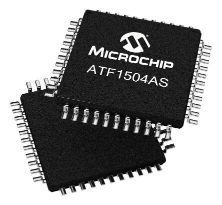
ICGOO在线商城 > 集成电路(IC) > 嵌入式 - CPLD(复杂可编程逻辑器件) > ATF1504AS-10AU44
 Datasheet下载
- 型号: ATF1504AS-10AU44
- 制造商: Atmel
- 库位|库存: xxxx|xxxx
- 要求:
| 数量阶梯 | 香港交货 | 国内含税 |
| +xxxx | $xxxx | ¥xxxx |
查看当月历史价格
查看今年历史价格
ATF1504AS-10AU44产品简介:
ICGOO电子元器件商城为您提供ATF1504AS-10AU44由Atmel设计生产,在icgoo商城现货销售,并且可以通过原厂、代理商等渠道进行代购。 ATF1504AS-10AU44价格参考。AtmelATF1504AS-10AU44封装/规格:嵌入式 - CPLD(复杂可编程逻辑器件), 。您可以下载ATF1504AS-10AU44参考资料、Datasheet数据手册功能说明书,资料中有ATF1504AS-10AU44 详细功能的应用电路图电压和使用方法及教程。
Microchip Technology的ATF1504AS-10AU44是一款嵌入式CPLD(复杂可编程逻辑器件),适用于多种场景,尤其适合需要灵活逻辑控制和小型化设计的应用。以下是其主要应用场景:

 1. 工业自动化
   - 在工业控制系统中,用于实现信号调理、协议转换或接口扩展。
   - 可用作简单的状态机控制器,管理传感器输入和执行器输出。

 2. 通信设备
   - 实现数据包处理、信号同步或时钟分频等功能。
   - 用于设计小型化的通信接口模块,例如UART到SPI/parallel的桥接。

 3. 消费电子
   - 提供定制化的逻辑功能,例如按键矩阵扫描、LED驱动或显示控制。
   - 在音频/视频设备中,用于格式转换或信号路由。

 4. 汽车电子
   - 用于CAN总线或其他车载网络的信号处理。
   - 实现简单的故障诊断逻辑或传感器信号预处理。

 5. 医疗设备
   - 用于小型医疗仪器中的信号采集与处理,例如心率监测仪或血糖仪。
   - 提供低功耗的逻辑控制解决方案。

 6. 嵌入式系统
   - 作为微控制器的辅助逻辑,扩展GPIO或实现特定功能。
   - 用于设计启动加载器或配置外围设备。

 7. 测试与测量
   - 在测试设备中,用于生成测试信号或捕获数据。
   - 实现触发逻辑或同步多个测试通道。

 特点总结:
- 小型封装:44引脚TQFP封装,适合空间受限的设计。
- 低功耗:适合电池供电设备。
- 灵活性:通过编程实现各种组合逻辑和时序逻辑。
- 可靠性:适用于恶劣环境下的工业和汽车应用。

这款CPLD特别适合对成本敏感且逻辑规模较小的应用场合,能够快速实现定制化功能,缩短开发周期。
| 参数 | 数值 |
| 产品目录 | 集成电路 (IC)半导体 |
| 描述 | IC CPLD 64MC 10NS 44TQFPCPLD - 复杂可编程逻辑器件 CPLD 64 MACROCELL w/ISP STD PWR 5V |
| 产品分类 | |
| I/O数 | 32 |
| 品牌 | Atmel |
| 产品手册 | |
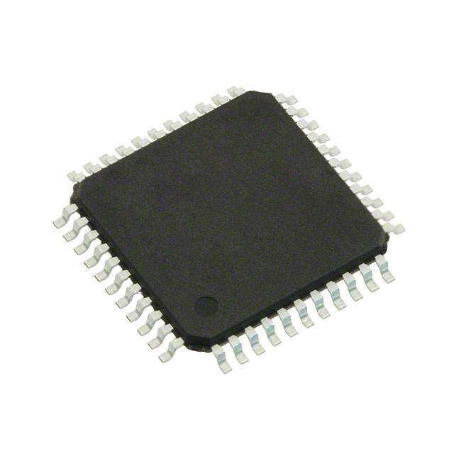
| 产品图片 |
|
| rohs | 符合RoHS无铅 / 符合限制有害物质指令(RoHS)规范要求 |
| 产品系列 | 嵌入式处理器和控制器,CPLD - 复杂可编程逻辑器件,Atmel ATF1504AS-10AU44ATF15xx |
| 数据手册 | |
| 产品型号 | ATF1504AS-10AU44 |
| 产品 | ATF1504AS |
| 产品目录页面 | |
| 产品种类 | CPLD - 复杂可编程逻辑器件 |
| 供应商器件封装 | 44-TQFP(10x10) |
| 其它名称 | ATF1504AS10AU44 |
| 包装 | 托盘 |
| 可编程类型 | 系统内可编程(最少 10,000 次编程/擦除循环) |
| 商标 | Atmel |
| 大电池数量 | 64 |
| 存储类型 | EEPROM |
| 安装类型 | 表面贴装 |
| 安装风格 | SMD/SMT |
| 宏单元数 | 64 |
| 封装/外壳 | 44-TQFP |
| 封装/箱体 | TQFP-44 |
| 工作温度 | -40°C ~ 85°C |
| 工作电源电压 | 5 V |
| 工作电源电流 | 130 mA |
| 工厂包装数量 | 160 |
| 延迟时间 | 10 ns |
| 延迟时间tpd(1)最大值 | 10.0ns |
| 最大工作温度 | + 85 C |
| 最大工作频率 | 125 MHz |
| 最小工作温度 | - 40 C |
| 栅极数 | - |
| 栅极数量 | 1500 |
| 标准包装 | 160 |
| 每个宏指令的积项数 | 5 |
| 电源电压-内部 | 4.5 V ~ 5.5 V |
| 电源电压-最大 | 5.5 V |
| 电源电压-最小 | 4.5 V |
| 输入/输出端数量 | 32 |
| 逻辑元件/块数 | - |
| 逻辑数组块数量——LAB | - |
| 配用 | /product-detail/zh/ATF15XX-DK3/ATF15XX-DK3-ND/1008628 |


- 商务部:美国ITC正式对集成电路等产品启动337调查
- 曝三星4nm工艺存在良率问题 高通将骁龙8 Gen1或转产台积电
- 太阳诱电将投资9.5亿元在常州建新厂生产MLCC 预计2023年完工
- 英特尔发布欧洲新工厂建设计划 深化IDM 2.0 战略
- 台积电先进制程称霸业界 有大客户加持明年业绩稳了
- 达到5530亿美元!SIA预计今年全球半导体销售额将创下新高
- 英特尔拟将自动驾驶子公司Mobileye上市 估值或超500亿美元
- 三星加码芯片和SET,合并消费电子和移动部门,撤换高东真等 CEO
- 三星电子宣布重大人事变动 还合并消费电子和移动部门
- 海关总署:前11个月进口集成电路产品价值2.52万亿元 增长14.8%


PDF Datasheet 数据手册内容提取
ATF1504AS and ATF1504ASL High-performance Complex Programmable Logic Device DATASHEET Features High-density, High-performance, Electrically-erasable Complex Programmable Logic Device ̶ 64 Macrocells ̶ 5 Product Terms per Macrocell, Expandable up to 40 per Macrocell ̶ 44, 84, 100 Pins ̶ 7.5ns Maximum Pin-to-pin Delay ̶ Registered Operation up to 125MHz ̶ Enhanced Routing Resources In-System Programmability (ISP) via JTAG Flexible Logic Macrocell ̶ D/T/Latch Configurable Flip-flops ̶ Global and Individual Register Control Signals ̶ Global and Individual Output Enable ̶ Programmable Output Slew Rate ̶ Programmable Output Open Collector Option ̶ Maximum Logic Utilization by Burying a Register with a COM Output Advanced Power Management Features ̶ Automatic μA Standby for “L” Version ̶ Pin-controlled 1mA Standby Mode ̶ Programmable Pin-keeper Circuits on Inputs and I/Os ̶ Reduced-power Feature per Macrocell Available in Commercial and Industrial Temperature Ranges Available in 44-lead and 84-lead PLCC; 44-lead and 100-lead TQFP Advanced EE Technology ̶ 100% Tested ̶ Completely Reprogrammable ̶ 10,000 Program/Erase Cycles ̶ 20 Year Data Retention ̶ 2000V ESD Protection ̶ 200mA Latch-up Immunity JTAG Boundary-scan Testing to IEEE Std. 1149.1-1990 and 1149.1a-1993 Supported PCI-compliant 3.3V or 5.0V I/O Pins Security Fuse Feature Green (Pb/Halide-free/RoHS Compliant) Package Options Atmel-0950P-CPLD-ATF1504AS(L)-Datasheet_032014
Enhanced Features Improved Connectivity (Additional Feedback Routing, Alternate Input Routing) Output Enable Product Terms Transparent — Latch Mode Combinatorial Output with Registered Feedback within Any Macrocell Three Global Clock Pins ITD (Input Transition Detection) Circuits on Global Clocks, Inputs, and I/O Fast Registered Input from Product Term Programmable “Pin-keeper” Option V Power-up Reset Option CC Pull-up Option on JTAG Pins TMS and TDI Advanced Power Management Features ̶ Edge-controlled Power-down “L” ̶ Individual Macrocell Power Option ̶ Disable ITD on Global Clocks, Inputs, and I/O Description The Atmel ®ATF1504AS(L) is a high-performance, high-density Complex Programmable Logic Device (CPLD) which utilizes the Atmel proven electrically-erasable memory technology. With 64 logic macrocells and up to 68 inputs, it easily integrates logic from several TTL, SSI, MSI, LSI, and classic PLDs. The ATF1504AS(L) enhanced routing switch matrices increases usable gate count and the odds of successful pin-locked design modifications. The ATF1504AS(L) has up to 68 bi-directional I/O pins and four dedicated input pins, depending on the type of device package selected. Each dedicated pin can also serve as a global control signal, register clock, register reset, or output enable. Each of these control signals can be selected for use individually within each macrocell. Each of the 64 macrocells generates a buried feedback which goes to the global bus. Each input and I/O pin also feeds into the global bus. The switch matrix in each logic block then selects 40 individual signals from the global bus. Each macrocell also generates a foldback logic term which goes to a regional bus. Cascade logic between macrocells in the ATF1504AS(L) allows fast, efficient generation of complex logic functions. The ATF1504AS(L) contains four such logic chains; each capable of creating sum term logic with a fan-in of up to 40 product terms. The ATF1504AS(L) macrocell, shown in Figure 1, is flexible enough to support highly-complex logic functions operating at high speed. The macrocell consists of five sections: Product Terms and Product Term Select Multiplexer OR/XOR/CASCADE Logic Flip-flop Output Select and Enable Logic Array Inputs 2 ATF1504AS(L) [DATASHEET] Atmel-0950P-CPLD-ATF1504AS(L)-Datasheet_032014
Figure 1. ATF1504AS(L) Macrocell ATF1504AS(L) [DATASHEET] 3 Atmel-0950P-CPLD-ATF1504AS(L)-Datasheet_032014
1. Pin Configurations and Pinouts Figure 1-1. Pinouts 44-lead TQFP 44-lead PLCC (Top View) (Top View) I/OI/OI/OVCCGCLK2/OE2/IGCLR/II/OE1GCLK1/IGNDGCLK3/I/OI/O I/OI/OI/OVCCGCLK2/OE2/IGCLR/IOE1/IGCLK1/IGNDGCLK3/I/OI/O 4443424140393837363534 TDI/I/O 7654321444342414039 I/O I/O/TDI 1 33 I/O I/O 8 38 I/O/TDO I/O 2 32 I/O/TDO I/O 9 37 I/O I/O 3 31 I/O GND 10 36 I/O GND 4 30 I/O PD1/I/O 11 35 VCC PD1/I/O 5 29 VCC I/O 12 34 I/O I/O 6 28 I/O I/O/TMS 13 33 I/O TMS/I/O 7 27 I/O I/O 14 32 I/O/TCK I/O 8 26 I/O/TCK VCC 15 31 I/O VCC 9 25 I/O I/O 16 30 GND I/O 10 24 GND I/O 17 29 I/O I/O 11 23 I/O 1819202122232425262728 12I/O13I/O14I/O15I/O16GND17VCC18I/O19D2/I/O20I/O21I/O22I/O I/OI/OI/OI/OGNDVCCI/OPD2/I/OI/OI/OI/O P 84-lead PLCC 100-lead TQFP (Top View) (Top View) I/O 1211I/O10I/O9I/O8I/O7GND6I/O5I/O4I/O3VCCINT2GCLK2/OE2/I1I/GCLR84I/OE183GCLK1/I82GND81GCLK3/I/O80I/O79I/O78VCCIO771/O76I/O75I/O74 I/O I/OI/OI/OI/OI/OGNDI/OI/OI/OVCCINTINPUT/OE2/GCLK2INPUT/GCLRINPUT/OE1INPUT/GCLK1GNDI/O/GCLK3I/OI/OVCCIOI/OI/OI/ONCNCI/O IV/OC/CTIDOI 1134 7732 IG/OND 100999897969594939291908988878685848382818079787776 I/O 15 71 I/O/TDO NC 1 75 I/O I/O 16 70 I/O NC 2 74 GND I/O 17 69 I/O VCCIO 3 73 I/O/TDO I/O 18 68 I/O I/O/TDI 4 72 NC GND 19 67 I/O NC 5 71 I/O I/O/PD1 20 66 VCCIO I/O 6 70 NC I/O 21 65 I/O NC 7 69 I/O I/O 22 64 I/O I/O 8 68 I/O I/O/TMS 23 63 I/O I/O 9 67 I/O I/O 24 62 I/O/TCK I/O 10 66 VCCIO I/O 25 61 I/O GND 11 65 I/O VCCIO 26 60 I/O I/O/PD1 12 64 I/O I/O 27 59 GND I/O 13 63 I/O I/O 28 58 I/O I/O 14 62 I/O/TCK I/O 29 57 I/O I/O/TMS 15 61 I/O I/O 30 56 I/O I/O 16 60 I/O I/O 31 55 I/O I/O 17 59 GND GND 32 54 I/O VCCIO 18 58 I/O 333435363738394041424344454647484950515253 I/O 19 57 I/O I/O 20 56 I/O I/OI/OI/OI/OI/OVCCIOI/OI/OI/OGNDVCCINTI/OI/OI/O/PD2GNDI/OI/OI/OI/OI/OVCCIO NII//OOC 222123 555543 NIN/OCC NC 24 52 I/O I/O 25 51 VCCIO 26272829303132333435363738394041424344454647484950 GNDNCNCI/OI/OI/OI/OI/OVCCIOI/OI/OI/OGNDVCCINTI/OI/OI/O/PD2GNDI/OI/OI/OI/OI/ONCNC Note: Drawings are not to scale. 4 ATF1504AS(L) [DATASHEET] Atmel-0950P-CPLD-ATF1504AS(L)-Datasheet_032014
2. Block Diagram Figure 2-1. Block Diagram Logic Block A gional dbacks Macrocells ReFol 1 to 16 I/O Pins hx Logic Block D SwitcMatri I/O Pins S) U B S K C A L B A D OBUSEE LBF Logic Block B G d Logic Block C n I/O Pins a I/O Pins S T U P N 5] 2] R Output (I R 2] 5] E[0: K[0: LEA ESnwaitbclhe LEA K[0: E[0: O C C C C O G G G Matrix G G G I/O (MC64)/GCLK3 Global Clock GCK[0:2] Mux INPUT/GCLK1 OE1/INPUT INPUT/OE2/GCLK2 Global Clock GCLEAR Mux INPUT/GCLR Unused product terms are automatically disabled by the compiler to decrease power consumption. A security fuse, when programmed, protects the contents of the ATF1504AS(L). Two bytes (16 bits) of User Signature are accessible to the user for purposes such as storing project name, part number, revision, or date. The User Signature is accessible regardless of the state of the security fuse. The ATF1504AS(L) device is an In-System Programmable (ISP) device. It uses the industry-standard 4-pin JTAG interface (IEEE Std. 1149.1), and is fully-compliant with JTAG’s Boundary-scan Description Language (BSDL). ISP allows the device to be programmed without removing it from the printed circuit board. In addition to simplifying the manufacturing flow, ISP also allows design modifications to be made in the field via software. ATF1504AS(L) [DATASHEET] 5 Atmel-0950P-CPLD-ATF1504AS(L)-Datasheet_032014
3. Macrocell Sections Table 3-1. Macrocell Sections Section Description Each ATF1504AS(L) macrocell has five product terms. Each product term receives as its possible inputs all signals from both the global bus and regional bus. Product Terms and The Product Term Select Multiplexer (PTMUX) allocates the five product terms as needed Select Mux to the macrocell logic gates and control signals. The PTMUX programming is determined by the design compiler, which selects the optimum macrocell configuration. The ATF1504AS(L) logic structure is designed to efficiently support all types of logic. Within a single macrocell, all the product terms can be routed to the OR gate, creating a 5-input AND/OR sum term. With the addition of the CASIN from neighboring macrocells, this can be expanded to as many as 40 product terms with a little small additional delay. The macrocell’s XOR gate allows efficient implementation of compare and arithmetic OR/XOR/CASCADE Logic functions. One input to the XOR comes from the OR sum term. The other XOR input can be a product term or a fixed high-level or low-level. For combinatorial outputs, the fixed level input allows polarity selection. For registered functions, the fixed levels allow DeMorgan minimization of product terms. The XOR gate is also used to emulate T-type and JK-type flip-flops. The ATF1504AS(L) flip-flop has very flexible data and control functions. The data input can come from either the XOR gate, from a separate product term, or directly from the I/O pin. Selecting the separate product term allows creation of a buried registered feedback within a combinatorial output macrocell. (This feature is automatically implemented by the fitter software). In addition to D, T, JK, and SR operation, the flip-flop can also be configured as a flow-through latch. In this mode, data passes through when the clock is high and is latched when the clock is low. Flip-flop The clock itself can either be one of the Global CLK Signals (GCK[0:2]) or an individual product term. The flip-flop changes state on the clock’s rising edge. When the GCK signal is used as the clock, one of the macrocell product terms can be selected as a clock enable. When the clock enable function is active and the enable signal (product term) is low, all clock edges are ignored. The flip-flop’s Asynchronous Reset signal (AR) can either be the Global Clear (GCLEAR), a product term, or always off. AR can also be a logic OR of GCLEAR with a product term. The Asynchronous Preset (AP) can be a product term or always off. The ATF1504AS(L) macrocell output can be selected as registered or combinatorial. The buried feedback signal can be either combinatorial or registered signal regardless of whether the output is combinatorial or registered. The output enable multiplexer (MOE) controls the output enable signals. Any buffer can be Output Select and Enable permanently enabled for simple output operation. Buffers can also be permanently disabled to allow use of the pin as an input. In this configuration all the macrocell resources are still available, including the buried feedback, expander, and CASCADE logic. The output enable for each macrocell can be selected as either of the two dedicated OE input pins as an I/O pin configured as an input, or as an individual product term. The global bus contains all input and I/O pin signals, as well as, the buried feedback signal from all 64 macrocells. The switch matrix in each logic block receives as its possible inputs Global Bus/Switch Matrix all signals from the global bus. Under software control, up to 40 of these signals can be selected as inputs to the logic block. Each macrocell also generates a foldback product term. This signal goes to the regional bus and is available to four macrocells. The foldback is an inverse polarity of one of the Foldback Bus macrocell’s product terms. The sixteen foldback terms in each region allow generation of high fan-in sum terms (up to sixteen product terms) with a nominal additional delay. 6 ATF1504AS(L) [DATASHEET] Atmel-0950P-CPLD-ATF1504AS(L)-Datasheet_032014
4. Programmable Pin-keeper Option for Inputs and I/Os The ATF1504AS(L) offers the option of programming all input and I/O pins so the pin-keeper circuits can be utilized. When any pin is driven high or low and then subsequently left floating, it will stay at that previous high-level or low-level. This circuitry prevents unused input and I/O lines from floating to intermediate voltage levels, which causes unnecessary power consumption and system noise. The keeper circuits eliminate the need for external pull-up resistors and eliminate their DC power consumption. Figure 4-1. Input Diagram V CC Input 100K ESD Protection Circuit Programmable Option Figure 4-2. I/O Diagram VCC OE Data I/O VCC 100K Programmable Option ATF1504AS(L) [DATASHEET] 7 Atmel-0950P-CPLD-ATF1504AS(L)-Datasheet_032014
5. Speed/Power Management The ATF1504AS(L) has several built-in speed and power management features. The ATF1504AS(L) contains circuitry which automatically puts the device into a low-power standby mode when no logic transitions are occurring. This not only reduces power consumption during inactive periods, but also provides proportional power savings for most applications running at system speeds below 5MHz. This feature may be selected as a device option. To further reduce power, each ATF1504AS(L) macrocell has a Reduced Power bit feature. This feature allows individual macrocells to be configured for maximum power savings. This feature may be selected as a design option. All ATF1504AS(L) have an optional power-down mode. In this mode, current drops to below 10mA. When the power-down option is selected, either PD1 or PD2 pins (or both) can be used to power-down the part. The power- down option is selected in the design source file. When enabled, the device goes into power-down when either PD1 or PD2 is high. In the power-down mode, all internal logic signals are latched and held, as are any enabled outputs. All pin transitions are ignored until the PD pin is brought low. When the power-down feature is enabled, the PD1 or PD2 pin cannot be used as a logic input or output; however, the pin’s macrocell may still be used to generate buried foldback and cascade logic signals. All power-down AC characteristic parameters are computed from external input or I/O pins, with Reduced Power bit turned on. For macrocells in reduced-power mode (Reduced Power bit turned on), the reduced-power adder, t , RPA must be added to the AC parameters, which include the data paths t , t , t , t , t , and t . LAD LAC IC ACL ACH SEXP The ATF1504AS(L) macrocell also has an option whereby the power can be reduced on a per macrocell basis. By enabling this power-down option, macrocells that are not used in an application can be turned-down, thereby reducing the overall power consumption of the device. Each output also has individual slew rate control. This may be used to reduce system noise by slowing down outputs that do not need to operate at maximum speed. Outputs default to slow switching, and may be specified as fast switching in the design file. 6. Design Software Support ATF1504AS(L) designs are supported by several industry-standard third-party tools. Automated fitters allow logic synthesis using a variety of high level description languages and formats. 7. Power-up Reset The ATF1504AS(L) is designed with a power-up reset, a feature critical for state machine initialization. At a point delayed slightly from V crossing V , all registers will be initialized, and the state of each output will CC RST depend on the polarity of its buffer. However, due to the asynchronous nature of reset and uncertainty of how V actually rises in the system, the following conditions are required: CC The V rise must be monotonic, CC After reset occurs, all input and feedback setup times must be met before driving the clock pin high, and, The clock must remain stable during T . D The ATF1504AS(L) has two options for the hysteresis about the reset level, V , Small and Large. During the RST fitting process users may configure the device with the Power-up Reset hysteresis set to Large or Small. Atmel POF2JED users may select the Large option by including the flag “-power_reset” on the command line after “filename.POF”. To allow the registers to be properly reinitialized with the Large hysteresis option selected, the following condition is added: If V falls below 2.0V, it must shut off completely before the device is turned on again. CC When the Large hysteresis option is active, I is reduced by several hundred micro amps as well. CC 8 ATF1504AS(L) [DATASHEET] Atmel-0950P-CPLD-ATF1504AS(L)-Datasheet_032014
8. Security Fuse Usage A single fuse is provided to prevent unauthorized copying of the ATF1504AS(L) fuse patterns. Once programmed, fuse verify is inhibited; however, the 16-bit User Signature remains accessible. 9. Programming ATF1504AS(L) devices are In-System Programmable (ISP) devices utilizing the 4-pin JTAG protocol. This capability eliminates package handling normally required for programming and facilitates rapid design iterations and field changes. Atmel provides ISP hardware and software to allow programming of the ATF1504AS(L) via the PC. ISP is performed by using either a download cable or a comparable board tester or a simple microprocessor interface. To facilitate ISP programming by the Automated Test Equipment (ATE) vendors. Serial Vector Format (SVF) files can be created by Atmel provided software utilities. ATF1504AS(L) devices can also be programmed using standard third-party programmers. With third-party programmer, the JTAG ISP port can be disabled thereby allowing four additional I/O pins to be used for logic. Contact your local Atmel representatives or Atmel PLD applications for details. 10. ISP Programming Protection The ATF1504AS(L) has a special feature which locks the device and prevents the inputs and I/O from driving if the programming process is interrupted for any reason. The inputs and I/O default to high-Z state during such a condition. In addition, the pin-keeper option preserves the former state during device programming if this circuit were previously programmed on the device. This prevents disturbing the operation of other circuits in the system while the ATF1504AS(L) is being programmed via ISP. All ATF1504AS(L) devices are initially shipped in the erased state thereby making them ready to use for ISP. Note: For more information refer to the “Designing for In-System Programmability with Atmel CPLDs” application note. ATF1504AS(L) [DATASHEET] 9 Atmel-0950P-CPLD-ATF1504AS(L)-Datasheet_032014
11. Electrical Characteristics 11.1 Absolute Maximum Ratings* Temperature Under Bias . . . . . . . . . . . . . . . .-40°C to +85°C *Notice: Stresses beyond those listed under “Absolute Maximum Ratings” may cause permanent Storage Temperature. . . . . . . . . . . . . . . . . .-65°C to +150°C damage to the device. This is a stress rating only and functional operation of the device at Voltage on Any Pin with these or any other conditions beyond those Respect to Ground. . . . . . . . . . . . . . . . . . . .-2.0V to +7.0V(1) indicated in the operational sections of this specification is not implied. Exposure to Voltage on Input Pins with Respect to Ground During Programming. . . . . . . . .-2.0V to +14.0V(1) absolute maximum rating conditions for extended periods may affect device reliability. Programming Voltage with Respect to Ground. . . . . . . . . . . . . . . . . . .-2.0V to +14.0V(1) Note: 1. Minimum voltage is -0.60VDC, which may undershoot to -2.0V for pulses of less than 20ns. Maximum output pin voltage is V + 0.75VDC, which may overshoot to 7.0V for pulses of less than 20ns. CC 11.2 Pin Capacitance Table 11-1. Pin Capacitance(1) Typ Max Units Conditions C 8 10 pF V = 0V; f = 1MHz IN IN C 8 10 pF V = 0V; f = 1MHz I/O OUT Note: 1. Typical values for nominal supply voltage. This parameter is only sampled and is not 100% tested. The OGI pin (high-voltage pin during programming) has a maximum capacitance of 12pF. 11.3 DC and AC Operating Conditions Table 11-2. DC and AC Operating Conditions Commercial Industrial Operating Temperature (Ambient) 0C to 70C -40C to 85C V or V (5.0V) Power Supply 5.0V± 5% 5.0V± 10% CCINT CCIO V (3.3V) Power Supply 3.0V to 3.6V 3.0V to 3.6V CCIO 10 ATF1504AS(L) [DATASHEET] Atmel-0950P-CPLD-ATF1504AS(L)-Datasheet_032014
11.4 DC Characteristics Table 11-3. DC Characteristics Symbol Parameter Condition Min Typ Max Units Input or I/O Low I V = V -2 -10 μA IL Leakage Current IN CC Input or I/O High I 2 10 IH Leakage Current Tri-state Output I V = V or GND -40 40 μA OZ Off-state Current O CC Com. 105 mA Std Mode Ind. 130 mA Power Supply Current, V = Max I CC CC1 Standby V = 0, V IN CC Com. 10 μA “L” Mode Ind. 10 μA Power Supply Current, V = Max I CC “PD” Mode 1 10 mA CC2 Power-down Mode V = 0, V IN CC Com 85 ma Current in Reduced-power V = Max I (2) CC Std Power CC3 Mode V = 0, V IN CC Ind 105 Com. 4.75 5.25 V V Supply Voltage 5.0V Device Output CCIO Ind. 4.50 5.50 V V Supply Voltage 3.3V Device Output 3.00 3.60 V CCIO V Input Low Voltage -0.30 0.80 V IL V Input High Voltage 2.00 V + 0.3 V IH CCIO Com. 0.45 V V = V or V Output Low Voltage (TTL) IN IH IL V = Min, I = 12mA CCIO OL Ind. V OL Com. 0.20 V V = V or V Output Low Voltage (CMOS) IN IH IL V = Min, I = 0.1mA CC OL Ind. 0.20 V V = V or V V Output High Voltage (TTL) IN IH IL 2.4 V OH V = Min, I = -4.0mA CCIO OH Notes: 1. Not more than one output at a time should be shorted. Duration of short circuit test should not exceed 30s. 2. When macrocell reduced-power feature is enabled. ATF1504AS(L) [DATASHEET] 11 Atmel-0950P-CPLD-ATF1504AS(L)-Datasheet_032014
11.5 AC Characteristics Table 11-4. AC Characteristics(1)(2) -7 -10 -25 Symbol Parameter Min Max Min Max Min Max Units Input or Feedback to t 7.5 10 25 ns PD1 Non-registered Output I/O Input or Feedback to t 7 9 25 ns PD2 Non-registered Feedback t Global Clock Setup Time 6 7 20 ns SU t Global Clock Hold Time 0 0 0 ns H Global Clock Setup Time of t 3 3 5 ns FSU Fast Input Global Clock Hold Time of t 0.5 0.5 2 ns FH Fast Input t Global Clock to Output Delay 4.5 5 13 ns COP t Global Clock High Time 3 4 7 ns CH t Global Clock Low Time 3 4 7 ns CL t Array Clock Setup Time 3 3 5 ns ASU t Array Clock Hold Time 2 3 6 ns AH t Array Clock Output Delay 7.5 10 25 ns ACOP t Array Clock High Time 3 4 10 ns ACH t Array Clock Low Time 3 4 10 ns ACL t Minimum Clock Global Period 8 10 22 ns CNT Maximum Internal Global f 125 100 50 MHz CNT Clock Frequency t Minimum Array Clock Period 8 10 22 ns ACNT Maximum Internal Array f 125 100 50 MHz ACNT Clock Frequency f Maximum Clock Frequency 166.7 125 60 MHz MAX t Input Pad and Buffer Delay 0.5 0.5 2 ns IN t I/O Input Pad and Buffer Delay 0.5 0.5 2 ns IO t Fast Input Delay 1 1 2 ns FIN t Foldback Term Delay 4 5 12 ns SEXP t Cascade Logic Delay 0.8 0.8 1.2 ns PEXP t Logic Array Delay 3 5 8 ns LAD Notes: 1. See ordering information for valid part numbers. 2. The t parameter must be added to the t , t ,t , t , and t parameters for macrocells running in RPA LAD LAC TIC ACL SEXP the reduced-power mode. 12 ATF1504AS(L) [DATASHEET] Atmel-0950P-CPLD-ATF1504AS(L)-Datasheet_032014
Table 11-4. AC Characteristics(1)(2) (Continued) -7 -10 -25 Symbol Parameter Min Max Min Max Min Max Units t Logic Control Delay 3 5 8 ns LAC t Internal Output Enable Delay 2 2 4 ns IOE Output Buffer and Pad Delay t (Slow slew rate = OFF; 2 1.5 6 ns OD1 V = 5.0V; C = 35pF) CCIO L Output Buffer and Pad Delay t (Slow slew rate = OFF; 2.5 2.0 7 ns OD2 V = 3.3V; C = 35pF) CCIO L Output Buffer and Pad Delay t (Slow slew rate = ON; 5 5.5 10 ns OD3 V = 5.0V or 3.3V; C = 35pF) CCIO L Output Buffer Enable Delay t (Slow slew rate = OFF; 4.0 5.0 10 ns ZX1 V = 5.0V; C = 35pF) CCIO L Output Buffer Enable Delay t (Slow slew rate = OFF; 4.5 5.5 10 ns ZX2 V = 3.3V; C = 35pF) CCIO L Output Buffer Enable Delay t (Slow slew rate = ON; 9 9 12 ns ZX3 V = 5.0V/3.3V; C = 35pF) CCIO L Output Buffer Disable Delay t 4 5 8 ns XZ (C = 5pF) L t Register Setup Time 3 3 6 ns SU t Register Hold Time 2 3 6 ns H t Register Setup Time of Fast Input 3 3 3 ns FSU t Register Hold Time of Fast Input 0.5 0.5 2.5 ns FH t Register Delay 1 2 2 ns RD t Combinatorial Delay 1 2 2 ns COMB t Array Clock Delay 3 5 8 ns IC t Register Enable Time 3 5 8 ns EN t Global Control Delay 1 1 1 ns GLOB t Register Preset Time 2 3 6 ns PRE t Register Clear Time 2 3 6 ns CLR t Switch Matrix Delay 1 1 2 ns UIM t Reduced-power Adder(2) 10 11 15 ns RPA Notes: 1. See ordering information for valid part numbers. 2. The t parameter must be added to the t , t ,t , t , and t parameters for macrocells running in RPA LAD LAC TIC ACL SEXP the reduced-power mode. ATF1504AS(L) [DATASHEET] 13 Atmel-0950P-CPLD-ATF1504AS(L)-Datasheet_032014
12. Timing Model Figure 12-1. Timing Model Internal Output Enable Delay tIOE Global Control Delay DIneplauyt tGLOB Cascade Logic RDegeilsatyer tIN Logic Array Delay tSU Output Switch Delay tPEXP tH Delay MtaUItMrix tLAD ttPCRLRE ttOODD12 Register Control tRD tOD3 DtteLtEIAClNaCy InpuFttFa DIsNetlay tttCFFSHOUMB ttttXZZZXXXZ123 Foldback Term Delay I/O tSEXP Delay tIO 12.1 Input Test Waveforms and Measurement Levels Figure 12-2. Input Test Waveforms and Measurement Levels 3.0V AC AC Driving 1.5V Measurement Levels Level 0.0V Note: t , t = 1.5ns typical R F 12.2 Output AC Test Loads Figure 12-3. Output AC Test Loads 5.0V R1 = 464Ω Output Pin R2 = 250Ω CL = 35pF 14 ATF1504AS(L) [DATASHEET] Atmel-0950P-CPLD-ATF1504AS(L)-Datasheet_032014
12.3 Power-down Mode The ATF1504AS(L) includes an optional pin-controlled power-down feature. When this mode is enabled, the PD pin acts as the power-down pin. When the PD pin is high, the device supply current is reduced to less than 10mA. During power-down, all output data and internal logic states are latched internally and held; therefore, all registered and combinatorial output data remain valid. Any outputs that were in a high-Z state at the onset will remain at high-Z. During power-down, all input signals except the power-down pin are blocked. Input and I/O hold latches remain active to ensure pins do not float to indeterminate levels, further reducing system power. The power-down mode feature is enabled in the logic design file or as a fitted or translated s/w option. Designs using the power-down pin may not use the PD pin as a logic array input; however, all other PD pin macrocell resources may still be used, including the buried feedback and foldback product term array inputs. 12.3.1 Power-down AC Characteristics Table 12-1. Power-down AC Characteristics(1)(2) -7 -10 -15 -20 -25 Symbol Parameter Min Max Min Max Min Max Min Max Min Max Units t Valid I, I/O before PD High 7 10 15 20 25 ns IVDH t Valid OE(2) before PD High 7 10 15 20 25 ns GVDH t Valid Clock(2) before PD High 7 10 15 20 25 ns CVDH t I, I/O Don’t Care after PD High 12 15 25 30 35 ns DHIX t OE(2) Don’t Care after PD High 12 15 25 30 35 ns DHGX t Clock(2) Don’t Care after PD High 12 15 25 30 35 ns DHCX t PD Low to Valid I, I/O 1 1 1 1 1 μs DLIV t PD Low to Valid OE (Pin or Term) 1 1 1 1 1 μs DLGV t PD Low to Valid Clock (Pin or Term) 1 1 1 1 1 μs DLCV t PD Low to Valid Output 1 1 1 1 1 μs DLOV Notes: 1. For slow slew outputs, add t . SSO 2. Pin or product term. 3. Includes t due to reduced power bit enabled. RPA ATF1504AS(L) [DATASHEET] 15 Atmel-0950P-CPLD-ATF1504AS(L)-Datasheet_032014
13. JTAG-BST/ISP Overview The JTAG boundary-scan testing is controlled by the Test Access Port (TAP) controller in the ATF1504AS(L). The boundary-scan technique involves the inclusion of a shift-register stage (contained in a boundary-scan cell) adjacent to each component so signals at component boundaries can be controlled and observed using scan testing principles. Each input pin and I/O pin has its own Boundary-Scan Cell (BSC) in order to support boundary scan testing. The ATF1504AS(L) does not currently include a Test Reset (TRST) input pin because the TAP controller is automatically reset at power-up. The five JTAG modes supported include: SAMPLE/PRELOAD EXTEST BYPASS IDCODE HIGHZ The ATF1504AS(L) ISP can fully be described using JTAG’s BSDL as described in IEEE Standard 1149.1b. This allows ATF1504AS(L) programming to be described and implemented using any one of the third-party development tools supporting this standard. The ATF1504AS(L) has the option of using four JTAG-standard I/O pins for boundary-scan testing (BST) and in-System Programming (ISP) purposes. The ATF1504AS(L) is programmable through the four JTAG pins using the IEEE standard JTAG programming protocol established by IEEE Standard 1149.1 using 5V TTL-level programming signals from the ISP interface for in-system programming. The JTAG feature is a programmable option. If JTAG (BST or ISP) is not needed, then the four JTAG control pins are available as I/O pins. 14. JTAG Boundary-Scan Cell (BSC) Testing The ATF1504AS(L) contains up to 68 I/O pins and four input pins depending on the device type and package type selected. Each input pin and I/O pin has its own BSC in order to support boundary-scan testing as described in detail by IEEE Standard 1149.1. A typical BSC consists of three capture registers or scan registers and up to two update registers. There are two types of BSCs, one for input or I/O pin and one for the macrocells. The BSCs in the device are chained together through the capture registers. Input to the capture register chain is fed in from the TDI pin while the output is directed to the TDO pin. Capture registers are used to capture active device data signals, to shift data in, and out of the device, and to load data into the update registers. Control signals are generated internally by the JTAG TAP controller. The BSC configuration for the input and I/O pins and macrocells are shown below. Figure 14-1. BSC Configuration for Input and I/O Pins (Except JTAG TAP Pins) Dedicated Input To Internal Logic 0 D Q TDO 1 Capture Registers Clock Shift TDI (From Next Register) Note: The ATF1504AS(L) has pull-up option on TMS and TDI pins. This feature is selected as a design option. 16 ATF1504AS(L) [DATASHEET] Atmel-0950P-CPLD-ATF1504AS(L)-Datasheet_032014
Figure 14-2. BSC Configuration for Macrocell Pin BSC TDO 0 D Q Pin 1 Capture DR TDI Clock Shift TDO OEJ 0 1 0 D Q D Q 1 OUTJ 0 1 Pin 0 D Q D Q 1 Capture Update DR DR TDI Mode Shift Clock Macrocell BSC ATF1504AS(L) [DATASHEET] 17 Atmel-0950P-CPLD-ATF1504AS(L)-Datasheet_032014
15. PCI Compliance The ATF1504AS(L) supports the growing need in the industry to support the new Peripheral Component Interconnect (PCI) interface standard in PCI-based designs and specifications. The PCI interface calls for high current drivers, which are much larger than the traditional TTL drivers. In general, PLDs and FPGAs parallel outputs to support the high current load required by the PCI interface. The ATF1504AS(L) allows this without contributing to system noise while delivering low output-to-output skew. Having a programmable high drive option is also possible without increasing output delay or pin capacitance. Figure 15-1. PCI Voltage-to-current Curves for Figure 15-2. PCI Voltage-to-current Curves for +5.0V Signaling in Pull-up Mode +5.0V Signaling in Pull-down Mode Pull Up Pull Down VCC VCC e Test Point e AC drive g g a a point olt olt V V 2.4 2.2 DC DC drive point drive point 1.4 AC drive 0.55 point Test Point -2 -44 Current (mA)-178 3,6 95 Current (mA)380 Table 15-1. PCI DC Characteristics Symbol Parameter Conditions Min Max Units V Supply Voltage 4.75 5.25 V CC V Input High Voltage 2.0 V + 0.5 V IH CC V Input Low Voltage -0.5 0.8 V IL I Input High Leakage Current V = 2.7V 70 μA IH IN I Input Low Leakage Current V = 0.5V -70 μA IL IN V Output High Voltage I = -2mA 2.4 V OH OUT V Output Low Voltage I = 3mA, 6mA 0.55 V OL OUT C Input Pin Capacitance 10 pF IN C CLK Pin Capacitance 12 pF CLK C IDSEL Pin Capacitance 8 pF IDSEL L Pin Inductance 20 nH PIN Note: 1. Leakage current is with pin-keeper off. 18 ATF1504AS(L) [DATASHEET] Atmel-0950P-CPLD-ATF1504AS(L)-Datasheet_032014
Table 15-2. PCI AC Characteristics Symbol Parameter Conditions Min Max Units 0 < V 1.4 -44 mA OUT Switching 1.4 < V < 2.4 -44+(V - 1.4)/0.024 mA OUT OUT I Current High OH(AC) (Test High) 3.1 < VOUT < VCC Equation A mA V = 3.1V -142 μA OUT V >2.2V 95 mA OUT Switching 2.2 > V > 0 V /0.023 mA OUT OUT I Current Low OL(AC) (Test Point) 0.1 > VOUT > 0 Equation B mA V = 0.71 206 mA OUT I Low Clamp Current -5 < V -1 -25+(V + 1)/0.015 mA CL IN IN SLEW Output Rise Slew Rate 0.4V to 2.4V load 0.5 3 V/ns R SLEW Output Fall Slew Rate 2.4V to 0.4V load 0.5 3 V/ns F Notes: 1. Equation A: I = 11.9 (V - 5.25) * (V + 2.45) for V > V > 3.1V. OH OUT OUT CC OUT 2. Equation B: I = 78.5 * V * (4.4 - V ) for 0V < V < 0.71V. OL OUT OUT OUT ATF1504AS(L) [DATASHEET] 19 Atmel-0950P-CPLD-ATF1504AS(L)-Datasheet_032014
16. Pinouts 16.1 ATF1504AS(L) Dedicated Pinouts 44-lead 44-lead 84-lead 100-lead Dedicated Pin TQFP J-lead J-lead TQFP INPUT/OE2/GCLK2 40 2 2 90 INPUT/GCLR 39 1 1 89 INPUT/OE1 38 44 84 88 INPUT/GCLK1 37 43 83 87 I/O /GCLK3 35 41 81 85 I/O/PD (1,2) 5, 19 11, 25 20, 46 12, 42 I/O/TDI (JTAG) 1 7 14 4 I/O/TMS (JTAG) 7 13 23 15 I/O/TCK (JTAG) 26 32 62 62 I/O/TDO (JTAG) 32 38 71 73 GND 4, 16, 24, 36 10, 22, 30, 42 7, 19, 32, 42, 47, 59, 72, 82 11, 26, 38, 43, 59, 74, 86, 95 V 9, 17, 29, 41 3, 15, 23, 35 3, 43 39, 91 CCINT V — — 13, 26, 38, 53, 66, 78 3, 18, 34, 51, 66, 82 CCIO 1, 2, 5, 7, 22, 24, 27, 28, 49, N/C — — — 50, 53, 55, 70, 72, 77, 78 # of Signal Pins 36 36 68 68 # User I/O Pins 32 32 64 64 Note: OE (1, 2) . . . . . . . . . . . . . Global OE Pins GCLR . . . . . . . . . . . . . . . Global Clear Pin GCLK (1, 2, 3). . . . . . . . . Global Clock Pins PD (1, 2) . . . . . . . . . . . . . Power-down pins TDI, TMS, TCK, TDO . . . JTAG pins used for boundary-scan testing or in-system programming GND . . . . . . . . . . . . . . . . Ground Pins V . . . . . . . . . . . . . . . V pins for the device (+5V - Internal) CCINT CC V . . . . . . . . . . . . . . . . V pins for output drivers (for I/O pins) (+5V or 3.3V - I/Os) CCIO CC 20 ATF1504AS(L) [DATASHEET] Atmel-0950P-CPLD-ATF1504AS(L)-Datasheet_032014
16.2 ATF1504AS(L) I/O Pinouts 44-lead 44-lead 84-lead 100-lead 44-lead 44-lead 84-lead 100-lead MC PLC PLCC TQFP PLCC TQFP MC PLC PLCC TQFP PLCC TQFP 1 A 12 6 22 14 33 C 24 18 44 40 2 A — — 21 13 34 C — — 45 41 3 A/PD1 11 5 20 12 35 C/PD2 25 19 46 42 4 A 9 3 18 10 36 C 26 20 48 44 5 A 8 2 17 9 37 C 27 21 49 45 6 A — — 16 8 38 C — — 50 46 7 A — — 15 6 39 C — — 51 47 8/TDI A 7 1 14 4 40 C 28 22 52 48 9 A — — 12 100 41 C 29 23 54 52 10 A — — 11 99 42 C — — 55 54 11 A 6 44 10 98 43 C — — 56 56 12 A — — 9 97 44 C — — 57 57 13 A — — 8 96 45 C — — 58 58 14 A 5 43 6 94 46 C 31 25 60 60 15 A — — 5 93 47 C — — 61 61 16 A 4 42 4 92 48/TCK C 32 26 62 62 17 B 21 15 41 37 49 D 33 27 63 63 18 B — — 40 36 50 D — — 64 64 19 B 20 14 39 35 51 D 34 28 65 65 20 B 19 13 37 33 52 D 36 30 67 67 21 B 18 12 36 32 53 D 37 31 68 68 22 B — — 35 31 54 D — — 69 69 23 B — — 34 30 55 D — — 70 71 24 B 17 11 33 29 56/TDO D 38 32 71 73 25 B 16 10 31 25 57 D 39 33 73 75 26 B — — 30 23 58 D — — 74 76 27 B — — 29 21 59 D — — 75 79 28 B — — 28 20 60 D — — 76 80 29 B — — 27 19 61 D — — 77 81 30 B 14 8 25 17 62 D 40 34 79 83 31 B — — 24 16 63 D — — 80 84 32/TMS B 13 7 23 15 64 D/GCLK3 41 35 81 85 ATF1504AS(L) [DATASHEET] 21 Atmel-0950P-CPLD-ATF1504AS(L)-Datasheet_032014
22 ATF1504AS(L) [DATASHEET] Atmel-0950P-CPLD-ATF1504AS(L)-Datasheet_032014
ATF1504AS(L) [DATASHEET] 23 Atmel-0950P-CPLD-ATF1504AS(L)-Datasheet_032014
24 ATF1504AS(L) [DATASHEET] Atmel-0950P-CPLD-ATF1504AS(L)-Datasheet_032014
17. Ordering Information 17.1 Green Package Options (Pb/Halide-free/RoHS Compliant) t t f PD CO1 MAX (ns) (ns) (MHz) Ordering Code Package Operation Range ATF1504AS-7AX44 44A Commercial 7.5 4.5 166.7 ATF1504AS-7JX44 44J (0C to 70C) ATF1504AS-7AX100 100A ATF1504AS-10AU44 44A Industrial ATF1504AS-10JU44 44J 10 5 125 (-40C to +85C) ATF1504AS-10AU100 100A ATF1504AS-10JU84 84J ATF1504ASL-25AU44 44A Industrial 25 15 70 ATF1504ASL-25JU44 44J (-40C to +85C) ATF1504ASL-25AU100 100A Package Type 44A 44-lead, Thin Plastic Gull Wing Quad Flatpack Package (TQFP) 44J 44-lead, Plastic J-leaded Chip Carrier (PLCC) 84J 84-lead, Plastic J-leaded Chip Carrier (PLCC) 100A 100-lead, 14 x 14mm body, Thin Profile Plastic Quad Flat Package (TQFP) ATF1504AS(L) [DATASHEET] 25 Atmel-0950P-CPLD-ATF1504AS(L)-Datasheet_032014
18. Packaging Information 18.1 44A — 44-lead TQFP D1 D e E E1 b BOTTOM VIEW TOP VIEW C 0°~7° A1 A2 A L SIDE VIEW COMMON DIMENSIONS (Unit of Measure = mm) SYMBOL MIN NOM MAX NOTE A – – 1.20 A1 0.05 – 0.15 A2 0.95 1.00 1.05 D 11.75 12.00 12.25 D1 9.90 10.00 10.10 Note 2 E 11.75 12.00 12.25 E1 9.90 10.00 10.10 Note 2 Notes: 1. This package conforms to JEDEC reference MS-026, Variation ACB. B 0.30 – 0.45 2. Dimensions D1 and E1 do not include mold protrusion. Allowable C 0.09 – 0.20 protrusion is 0.25 mm per side. Dimensions D1 and E1 are maximum plastic body size dimensions including mold mismatch. L 0.45 – 0.75 3. Lead coplanarity is 0.10 mm maximum. e 0.80 TYP 1/10/13 TITLE GPC DRAWING NO. REV. 44A, 44-lead 10.0 x 10.0x1.0 mm Body, 0.80 mm Package Drawing Contact: Lead Pitch, Thin Profile Plastic Quad Flat AIX 44A D packagedrawings@atmel.com Package (TQFP) 26 ATF1504AS(L) [DATASHEET] Atmel-0950P-CPLD-ATF1504AS(L)-Datasheet_032014
18.2 44J — 44-lead PLCC 1.14(0.045) X 45° 1.14(0.045) X 45° PIN NO. 1 0.318(0.0125) IDENTIFIER 0.191(0.0075) E1 E B1 D2/E2 B e A2 D1 A1 D A 0.51(0.020)MAX 45° MAX (3X) COMMON DIMENSIONS (Unit of Measure = mm) SYMBOL MIN NOM MAX NOTE A 4.191 – 4.572 A1 2.286 – 3.048 A2 0.508 – – D 17.399 – 17.653 D1 16.510 – 16.662 Note 2 E 17.399 – 17.653 Notes: 1. This package conforms to JEDEC reference MS-018, Variation AC. E1 16.510 – 16.662 Note 2 2. Dimensions D1 and E1 do not include mold protrusion. Allowable protrusion is .010"(0.254 mm) per side. Dimension D1 D2/E2 14.986 – 16.002 and E1 include mold mismatch and are measured at the extreme B 0.660 – 0.813 material condition at the upper or lower parting line. 3. Lead coplanarity is 0.004" (0.102 mm) maximum. B1 0.330 – 0.533 e 1.270 TYP 10/04/01 TITLE DRAWING NO. REV. Package Drawing Contact: 44J, 44-lead, Plastic J-leaded Chip Carrier (PLCC) 44J B packagedrawings@atmel.com ATF1504AS(L) [DATASHEET] 27 Atmel-0950P-CPLD-ATF1504AS(L)-Datasheet_032014
18.3 84J — 84-lead PLCC 1.14(0.045) X 45° 1.14(0.045) X 45° PIN NO. 1 0.318(0.0125) IDENTIFIER 0.191(0.0075) E1 E B1 D2/E2 B e A2 D1 A1 D A 0.51(0.020)MAX 45° MAX (3X) COMMON DIMENSIONS (Unit of Measure = mm) SYMBOL MIN NOM MAX NOTE A 4.191 – 4.572 A1 2.286 – 3.048 A2 0.508 – – D 30.099 – 30.353 D1 29.210 – 29.413 Note 2 Notes: 1. This package conforms to JEDEC reference MS-018, Variation AF. E 30.099 – 30.353 2. Dimensions D1 and E1 do not include mold protrusion. E1 29.210 – 29.413 Note 2 Allowable protrusion is .010"(0.254 mm) per side. Dimension D1 and E1 include mold mismatch and are measured at the extreme D2/E2 27.686 – 28.702 material condition at the upper or lower parting line. B 0.660 – 0.813 3. Lead coplanarity is 0.004" (0.102 mm) maximum. B1 0.330 – 0.533 e 1.270 TYP 10/04/01 TITLE DRAWING NO. REV. Package Drawing Contact: 84J, 84-lead, Plastic J-leaded Chip Carrier (PLCC) 84J B packagedrawings@atmel.com 28 ATF1504AS(L) [DATASHEET] Atmel-0950P-CPLD-ATF1504AS(L)-Datasheet_032014
18.4 100A — 100-lead TQFP D1 D e E E1 b Bottom View Top View A2 C 0°~7° COMMON DIMENSIONS (Unit of Measure = mm) L A A SYMBOL MIN NOM MAX NOTE 1 A – – 1.20 Side View A1 0.05 – 0.15 A2 0.95 1.00 1.05 D 16.00 BSC D1 14.00 BSC Note 2 E 16.00 BSC E1 14.00 BSC Note 2 Notes: 1. This package conforms to JEDEC reference MS-026, b 0.17 0.22 0.27 Variation AED. 2. Dimensions D1 and E1 do not include mold protrusion. C 0.09 – 0.20 Allowable protrusion is 0.25 mm per side. Dimensions D1 L 0.45 0.60 0.75 and E1 are maximum plastic body size dimensions including mold mismatch. e 0.50 TYP 3. Lead coplanarity is 0.10 mm maximum. 09/26/11 TITLE GPC DRAWING NO. REV. 100A, 100-lead 14.0 x 14.0 x 1.0 mm Body, 0.50 mm Package Drawing Contact: Lead Pitch, Thin Profile Plastic Quad Flat AAD 100A D packagedrawings@atmel.com Package (TQFP) ATF1504AS(L) [DATASHEET] 29 Atmel-0950P-CPLD-ATF1504AS(L)-Datasheet_032014
19. Revision History Doc. Rev. Date Comments Add ATF1504AS-7AX100 ordering code. 0950P 03/2014 Remove 68-pin PLCC and 100-pin PQFP packages and -15 and -20ns speed grades. Update template, logo, and disclaimer page. 0950O 07/2006 Add Green package options. 30 ATF1504AS(L) [DATASHEET] Atmel-0950P-CPLD-ATF1504AS(L)-Datasheet_032014
X X X X X X Atmel Corporation 1600 Technology Drive, San Jose, CA 95110 USA T: (+1)(408) 441.0311 F: (+1)(408) 436.4200 | www.atmel.com © 2014 Atmel Corporation. / Rev.: Atmel-0950P-CPLD-ATF1504AS(L)-Datasheet_032014. Atmel®, Atmel logo and combinations thereof, and others are registered trademarks or trademarks of Atmel Corporation or its subsidiaries. Other terms and product names may be trademarks of others. DISCLAIMER: The information in this document is provided in connection with Atmel products. No license, express or implied, by estoppel or otherwise, to any intellectual property right is granted by this document or in connection with the sale of Atmel products. EXCEPT AS SET FORTH IN THE ATMEL TERMS AND CONDITIONS OF SALES LOCATED ON THE ATMEL WEBSITE, ATMEL ASSUMES NO LIABILITY WHATSOEVER AND DISCLAIMS ANY EXPRESS, IMPLIED OR STATUTORY WARRANTY RELATING TO ITS PRODUCTS INCLUDING, BUT NOT LIMITED TO, THE IMPLIED WARRANTY OF MERCHANTABILITY, FITNESS FOR A PARTICULAR PURPOSE, OR NON-INFRINGEMENT. IN NO EVENT SHALL ATMEL BE LIABLE FOR ANY DIRECT, INDIRECT, CONSEQUENTIAL, PUNITIVE, SPECIAL OR INCIDENTAL DAMAGES (INCLUDING, WITHOUT LIMITATION, DAMAGES FOR LOSS AND PROFITS, BUSINESS INTERRUPTION, OR LOSS OF INFORMATION) ARISING OUT OF THE USE OR INABILITY TO USE THIS DOCUMENT, EVEN IF ATMEL HAS BEEN ADVISED OF THE POSSIBILITY OF SUCH DAMAGES. Atmel makes no representations or warranties with respect to the accuracy or completeness of the contents of this document and reserves the right to make changes to specifications and products descriptions at any time without notice. Atmel does not make any commitment to update the information contained herein. Unless specifically provided otherwise, Atmel products are not suitable for, and shall not be used in, automotive applications. Atmel products are not intended, authorized, or warranted for use as components in applications intended to support or sustain life. SAFETY-CRITICAL, MILITARY, AND AUTOMOTIVE APPLICATIONS DISCLAIMER: Atmel products are not designed for and will not be used in connection with any applications where the failure of such products would reasonably be expected to result in significant personal injury or death (“Safety-Critical Applications”) without an Atmel officer's specific written consent. Safety-Critical Applications include, without limitation, life support devices and systems, equipment or systems for the operation of nuclear facilities and weapons systems. Atmel products are not designed nor intended for use in military or aerospace applications or environments unless specifically designated by Atmel as military-grade. Atmel products are not designed nor intended for use in automotive applications unless specifically designated by Atmel as automotive-grade.
Mouser Electronics Authorized Distributor Click to View Pricing, Inventory, Delivery & Lifecycle Information: M icrochip: ATF1504AS-10JC44 ATF1504AS-15JI44 ATF1504AS-7AC44 ATF1504AS-10JI44 ATF1504AS-10AC44 ATF1504AS-10AC100 ATF1504AS-15AC100 ATF1504AS15AI100 ATF1504AS-10AI100 ATF1504AS-10AU100 ATF1504AS-10AU44 ATF1504AS-10JC84 ATF1504AS-10JI84 ATF1504AS-10JU44 ATF1504AS-10JU84 ATF1504AS-15AC44 ATF1504AS-15JC44 ATF1504AS-15JC84 ATF1504AS-15JI68 ATF1504AS-15JI84 ATF1504AS-15QC100 ATF1504AS-15QI100 ATF1504AS-7AC100 ATF1504AS-7AX100 ATF1504AS-7AX44 ATF1504AS-7JC68 ATF1504AS-7JC84 ATF1504AS-7QC100 ATF1504ASL-20AC100 ATF1504ASL-20AC44 ATF1504ASL-20JC44 ATF1504ASL-20JC68 ATF1504ASL-20JC84 ATF1504ASL-20QC100 ATF1504ASL-25AI100 ATF1504ASL-25AI44 ATF1504ASL-25AU100 ATF1504ASL-25AU44 ATF1504ASL-25JI44 ATF1504ASL-25JI68 ATF1504ASL-25JI84 ATF1504ASL-25JU44 ATF1504AS-15AI100 ATF1504AS-7JX44 ATF1504AS-15JC68 ATF1504AS-10JI68 ATF1504AS-10JC68 ATF1504ASL-25AU44-T