ICGOO在线商城 > 集成电路(IC) > 嵌入式 - FPGA(现场可编程门阵列) > XC6SLX150T-3CSG484C
 Datasheet下载
- 型号: XC6SLX150T-3CSG484C
- 制造商: Xilinx
- 库位|库存: xxxx|xxxx
- 要求:
| 数量阶梯 | 香港交货 | 国内含税 |
| +xxxx | $xxxx | ¥xxxx |
查看当月历史价格
查看今年历史价格
XC6SLX150T-3CSG484C产品简介:
ICGOO电子元器件商城为您提供XC6SLX150T-3CSG484C由Xilinx设计生产,在icgoo商城现货销售,并且可以通过原厂、代理商等渠道进行代购。 XC6SLX150T-3CSG484C价格参考。XilinxXC6SLX150T-3CSG484C封装/规格:嵌入式 - FPGA(现场可编程门阵列), 。您可以下载XC6SLX150T-3CSG484C参考资料、Datasheet数据手册功能说明书,资料中有XC6SLX150T-3CSG484C 详细功能的应用电路图电压和使用方法及教程。
Xilinx Inc.(赛灵思公司)生产的XC6SLX150T-3CSG484C属于Spartan-6系列FPGA(现场可编程门阵列),是一款高性能、低功耗的嵌入式器件。其应用场景广泛,尤其适合对成本和性能有平衡需求的领域。以下是该型号FPGA的主要应用场景:

 1. 工业自动化
   - 应用:运动控制、机器人、PLC(可编程逻辑控制器)、工业通信协议(如EtherCAT、Profinet)。
   - 特点:XC6SLX150T具有丰富的I/O资源和灵活的逻辑单元,能够实现复杂的实时控制和数据处理任务。

 2. 通信设备
   - 应用:小型基站、无线通信模块、网络接口卡(NIC)。
   - 特点:支持高速串行接口(如GTX收发器),可用于数据传输速率要求较高的场景。

 3. 消费电子
   - 应用:高清视频处理、图像识别、多媒体播放器。
   - 特点:集成DSP Slice(数字信号处理模块),适合处理音频、视频等多媒体信号。

 4. 医疗设备
   - 应用:医学成像(如超声波、CT扫描)、患者监护系统。
   - 特点:提供高可靠性与低延迟的数据处理能力,满足医疗设备对精度和实时性的要求。

 5. 汽车电子
   - 应用:高级驾驶辅助系统(ADAS)、车载信息娱乐系统。
   - 特点:支持多种传感器数据融合,具备良好的环境适应性和稳定性。

 6. 航空航天与国防
   - 应用:导航系统、雷达信号处理、加密通信。
   - 特点:具备抗辐射选型(部分产品线),适用于苛刻环境下的关键任务。

 7. 测试与测量
   - 应用:数据采集系统、信号发生器、示波器。
   - 特点:支持高速数据采集和处理,同时具备灵活的用户自定义功能。

 总结
XC6SLX150T-3CSG484C凭借其强大的逻辑资源(约15万逻辑单元)、内置块RAM、DSP Slice以及丰富的外设接口,成为许多嵌入式系统的理想选择。它特别适合需要高效数据处理、复杂算法实现以及多协议支持的应用场景。此外,其较低的成本和功耗也使其在中端市场具有显著的竞争优势。
| 参数 | 数值 |
| 产品目录 | 集成电路 (IC) |
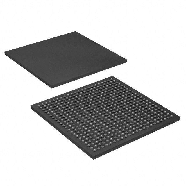
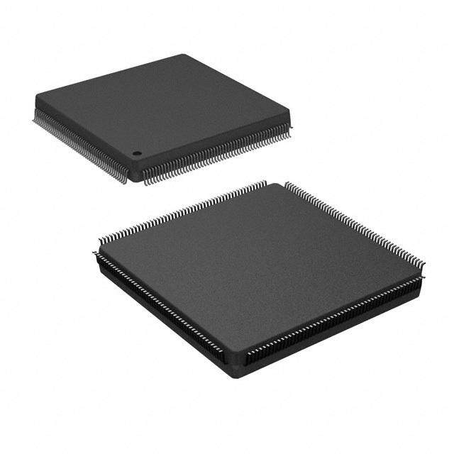
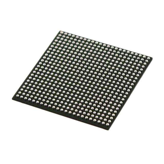
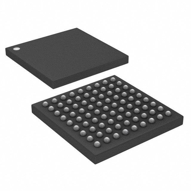
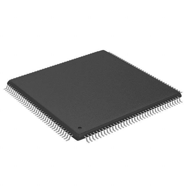
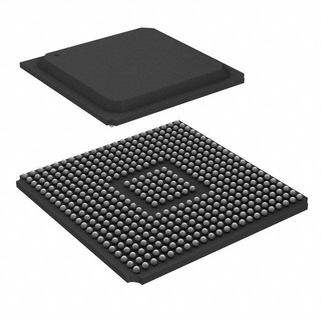
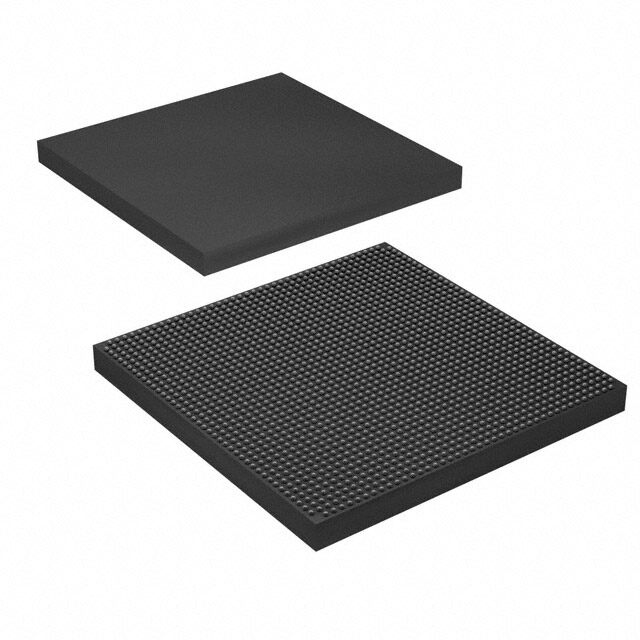
| 描述 | IC FPGA 296 I/O 484CSPBGA |
| 产品分类 | |
| I/O数 | 296 |
| LAB/CLB数 | 11519 |
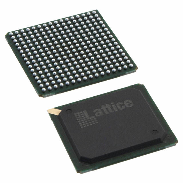
| 品牌 | Xilinx Inc |
| 数据手册 | |
| 产品图片 |
|
| 产品型号 | XC6SLX150T-3CSG484C |
| PCN设计/规格 | |
| rohs | 无铅 / 符合限制有害物质指令(RoHS)规范要求 |
| 产品系列 | Spartan® 6 LXT |
| 供应商器件封装 | 484-CSPBGA(19x19) |
| 其它名称 | 122-1792 |
| 安装类型 | 表面贴装 |
| 封装/外壳 | 484-FBGA,CSPBGA |
| 工作温度 | 0°C ~ 85°C |
| 总RAM位数 | 4939776 |
| 栅极数 | - |
| 标准包装 | 84 |
| 电压-电源 | 1.14 V ~ 1.26 V |
| 逻辑元件/单元数 | 147443 |


- 商务部:美国ITC正式对集成电路等产品启动337调查
- 曝三星4nm工艺存在良率问题 高通将骁龙8 Gen1或转产台积电
- 太阳诱电将投资9.5亿元在常州建新厂生产MLCC 预计2023年完工
- 英特尔发布欧洲新工厂建设计划 深化IDM 2.0 战略
- 台积电先进制程称霸业界 有大客户加持明年业绩稳了
- 达到5530亿美元!SIA预计今年全球半导体销售额将创下新高
- 英特尔拟将自动驾驶子公司Mobileye上市 估值或超500亿美元
- 三星加码芯片和SET,合并消费电子和移动部门,撤换高东真等 CEO
- 三星电子宣布重大人事变动 还合并消费电子和移动部门
- 海关总署:前11个月进口集成电路产品价值2.52万亿元 增长14.8%


PDF Datasheet 数据手册内容提取
89 Spartan-6 FPGA Data Sheet: DC and Switching Characteristics DS162 (v3.1.1) January 30, 2015 Product Specification Spartan-6 FPGA Electrical Characteristics Spartan®-6 LX and LXT FPGAs are available in various speed grades, with -3 having the highest performance. The DC and AC electrical parameters of the Automotive XA Spartan-6 FPGAs and Defense-grade Spartan-6Q FPGAs devices are equivalent to the commercial specifications except where noted. The timing characteristics of the commercial (XC) -2 speed grade industrial device are the same as for a -2 speed grade commercial device. The -2Q and -3Q speed grades are exclusively for the expanded (Q) temperature range. The timing characteristics are equivalent to those shown for the -2 and -3 speed grades for the Automotive and Defense-grade devices. Spartan-6FPGA DC and AC characteristics are specified for commercial (C), industrial (I), and expanded (Q) temperature ranges. Only selected speed grades and/or devices might be available in the industrial or expanded temperature ranges for Automotive and Defense-grade devices. References to device names refer to all available variations of that part number (for example, LX75 could denote XC6SLX75, XA6SLX75, or XQ6SLX75). The Spartan-6 FPGA -3N speed grade designates devices that do not support MCB functionality. All supply voltage and junction temperature specifications are representative of worst-case conditions. The parameters included are common to popular designs and typical applications. Available device and package combinations can be found at: (cid:129) DS160: Spartan-6 Family Overview (cid:129) DS170: Automotive XA Spartan-6 Family Overview (cid:129) DS172: Defense-Grade Spartan-6Q Family Overview This Spartan-6 FPGA data sheet, part of an overall set of documentation on the Spartan-6 family of FPGAs, is available on the Xilinx website at http://www.xilinx.com/support/documentation/spartan-6.htm. Spartan-6 FPGA DC Characteristics Table 1: Absolute Maximum Ratings(1) Symbol Description Units V Internal supply voltage relative to GND –0.5 to 1.32 V CCINT V Auxiliary supply voltage relative to GND –0.5 to 3.75 V CCAUX V Output drivers supply voltage relative to GND –0.5 to 3.75 V CCO V Key memory battery backup supply (LX75, LX75T, LX100, LX100T, LX150, and LX150T only) –0.5 to 4.05 V BATT External voltage supply for eFUSE programming (LX75, LX75T, LX100, LX100T, LX150, and –0.5 to 3.75 V V FS LX150T only)(2) V Input reference voltage –0.5 to 3.75 V REF © 2009–2015 Xilinx, Inc. XILINX, the Xilinx logo, Virtex, Zynq, Artix, Kintex, Spartan, ISE, and other designated brands included herein are trademarks of Xilinx in the United States and other countries. All other trademarks are the property of their respective owners. DS162 (v3.1.1) January 30, 2015 www.xilinx.com Product Specification 1
Spartan-6 FPGA Data Sheet: DC and Switching Characteristics Table 1: Absolute Maximum Ratings(1) (Cont’d) Symbol Description Units DC –0.60 to 4.10 V Commercial 20% overshoot duration –0.75 to 4.25 V 8% overshoot duration(5) –0.75 to 4.40 V DC –0.60 to 3.95 V All user and dedicated Industrial 20% overshoot duration –0.75 to 4.15 V I/Os 4% overshoot duration(5) –0.75 to 4.40 V DC –0.60 to 3.95 V Expanded (Q) 20% overshoot duration –0.75 to 4.15 V I/O input voltage or voltage 4% overshoot duration(5) –0.75 to 4.40 V V and V (3) applied to 3-state output, IN TS relative to GND(4) 20% overshoot duration –0.75 to 4.35 V Commercial 15% overshoot duration(5) –0.75 to 4.40 V 10% overshoot duration –0.75 to 4.45 V 20% overshoot duration –0.75 to 4.25 V Restricted to maximum of 100 user Industrial 10% overshoot duration –0.75 to 4.35 V I/Os 8% overshoot duration(5) –0.75 to 4.40 V 20% overshoot duration –0.75 to 4.25 V Expanded (Q) 10% overshoot duration –0.75 to 4.35 V 8% overshoot duration(5) –0.75 to 4.40 V T Storage temperature (ambient) –65to150 °C STG Maximum soldering temperature(6) +260 °C (TQG144, CPG196, CSG225, CSG324, CSG484, and FTG256) T SOL Maximum soldering temperature(6) (Pb-free packages: FGG484, FGG676, and FGG900) +250 °C Maximum soldering temperature(6) (Pb packages: CS484, FT256, FG484, FG676, and FG900) +220 °C T Maximum junction temperature(6) +125 °C j Notes: 1. Stresses beyond those listed under Absolute Maximum Ratings might cause permanent damage to the device. These are stress ratings only, and functional operation of the device at these or any other conditions beyond those listed under Operating Conditions is not implied. Exposure to Absolute Maximum Ratings conditions for extended periods of time might affect device reliability. 2. When programming eFUSE, V ≤V . Requires up to 40mA current. For read mode, V can be between GND and 3.45V. FS CCAUX FS 3. I/O absolute maximum limit applied to DC and AC signals. Overshoot duration is the percentage of a data period that the I/O is stressed beyond 3.45V. 4. For I/O operation, refer to UG381: Spartan-6 FPGA SelectIO Resources User Guide. 5. Maximum percent overshoot duration to meet 4.40V maximum. 6. T is the maximum soldering temperature for component bodies. For soldering guidelines and thermal considerations, SOL see UG385: Spartan-6 FPGA Packaging and Pinout Specification. DS162 (v3.1.1) January 30, 2015 www.xilinx.com Product Specification 2
Spartan-6 FPGA Data Sheet: DC and Switching Characteristics Table 2: Recommended Operating Conditions(1) Symbol Description Min Typ Max Units -3, -3N, -2 Standard performance(2) 1.14 1.2 1.26 V V Internal supply voltage relative to GND -3, -2 Extended performance(2) 1.2 1.23 1.26 V CCINT -1L Standard performance(2) 0.95 1.0 1.05 V V =2.5V(5) 2.375 2.5 2.625 V CCAUX V (3)(4) Auxiliary supply voltage relative to GND CCAUX V =3.3V 3.15 3.3 3.45 V CCAUX V (6)(7)(8) Output supply voltage relative to GND 1.1 – 3.45 V CCO Commercial temperature (C) –0.5 – 4.0 V All I/O standards Industrial temperature (I) –0.5 – 3.95 V VIN Input voltage relative to GND (except PCI) Expanded (Q) temperature –0.5 – 3.95 V PCI I/O standard(9) –0.5 – V +0.5 V CCO Maximum current through pin using PCI I/O standard Commercial (C) and – – 10 mA when forward biasing the clamp diode.(9) Industrial temperature (I) I (10) IN Expanded (Q) temperature – – 7 mA Maximum current through pin when forward biasing the ground clamp diode. – – 10 mA Battery voltage relative to GND, T =0°C to +85°C V (11) j 1.0 – 3.6 V BATT (LX75, LX75T, LX100, LX100T, LX150, and LX150T only) Commercial (C) range 0 – 85 °C T Junction temperature operating range Industrial temperature (I) range –40 – 100 °C j Expanded (Q) temperature range –40 – 125 °C Notes: 1. All voltages are relative to ground. 2. See Interface Performances for Memory Interfaces in Table25. The extended performance range is specified for designs not using the standard V voltage range. The standard V voltage range is used for: CCINT CCINT (cid:129) Designs that do not use an MCB (cid:129) LX4 devices (cid:129) Devices in the TQG144 or CPG196 packages (cid:129) Devices with the -3N speed grade 3. Recommended maximum voltage droop for V is 10mV/ms. CCAUX 4. During configuration, if V is 1.8V, then V must be 2.5V. CCO_2 CCAUX 5. The -1L devices require V =2.5V when using the LVDS_25, LVDS_33, BLVDS_25, LVPECL_25, RSDS_25, RSDS_33, PPDS_25, CCAUX and PPDS_33 I/O standards on inputs. LVPECL_33 is not supported in the -1L devices. 6. Configuration data is retained even if V drops to 0V. CCO 7. Includes V of 1.2V, 1.5V, 1.8V, 2.5V, and 3.3V. CCO 8. For PCI systems, the transmitter and receiver should have common supplies for V . CCO 9. Devices with a -1L speed grade do not support Xilinx PCI IP. 10. Do not exceed a total of 100mA per bank. 11. V is required to maintain the battery backed RAM (BBR) AES key when V is not applied. Once V is applied, V can be BATT CCAUX CCAUX BATT unconnected. When BBR is not used, Xilinx recommends connecting to V or GND. However, V can be unconnected. CCAUX BATT DS162 (v3.1.1) January 30, 2015 www.xilinx.com Product Specification 3
Spartan-6 FPGA Data Sheet: DC and Switching Characteristics Table 3: eFUSE Programming Conditions(1) Symbol Description Min Typ Max Units V (2) External voltage supply 3.2 3.3 3.4 V FS I V supply current – – 40 mA FS FS V Auxiliary supply voltage relative to GND 3.2 3.3 3.45 V CCAUX R (3) External resistor from R pin to GND 1129 1140 1151 Ω FUSE FUSE V Internal supply voltage relative to GND 1.14 1.2 1.26 V CCINT t Temperature range 15 – 85 °C j Notes: 1. These specifications apply during programming of the eFUSE AES key. Programming is only supported through JTAG.The AES key is only supported in the following devices: LX75, LX75T, LX100, LX100T, LX150, and LX150T. 2. When programming eFUSE, V must be less than or equal to V . When not programming or when eFUSE is not used, Xilinx FS CCAUX recommends connecting V to GND. However, V can be between GND and 3.45V. FS FS 3. An R resistor is required when programming the eFUSE AES key. When not programming or when eFUSE is not used, Xilinx FUSE recommends connecting the R pin to V or GND. However, R can be unconnected. FUSE CCAUX FUSE DS162 (v3.1.1) January 30, 2015 www.xilinx.com Product Specification 4
Spartan-6 FPGA Data Sheet: DC and Switching Characteristics Table 4: DC Characteristics Over Recommended Operating Conditions Symbol Description Min Typ Max Units V Data retention V voltage (below which configuration data might be lost) 0.8 – – V DRINT CCINT V Data retention V voltage (below which configuration data might be lost) 2.0 – – V DRAUX CCAUX V leakage current per pin for commercial (C) and industrial (I) devices –10 – 10 µA REF I REF V leakage current per pin for expanded (Q) devices –15 – 15 µA REF Input or output leakage current per pin (sample-tested) for commercial (C) and industrial –10 – 10 µA I (I) devices L Input or output leakage current per pin (sample-tested) for expanded (Q) devices –15 – 15 µA All pins except PROGRAM_B, DONE, and –20 – 20 µA Leakage current on pins during hot JTAG pins when HSWAPEN=1 I HS socketing with FPGA unpowered PROGRAM_B, DONE, and JTAG pins, or other I + µA HS(HSWAPEN = 1) pins when HSWAPEN=0 I RPU C (1) Die input capacitance at the pad – – 10 pF IN Pad pull-up (when selected) @ V =0V, V =3.3V or V =3.3V 200 – 500 µA IN CCO CCAUX Pad pull-up (when selected) @ V =0V, V =2.5V or V =2.5V 120 – 350 µA IN CCO CCAUX I Pad pull-up (when selected) @ V =0V, V =1.8V 60 – 200 µA RPU IN CCO Pad pull-up (when selected) @ V =0V, V =1.5V 40 – 150 µA IN CCO Pad pull-up (when selected) @ V =0V, V =1.2V 12 – 100 µA IN CCO Pad pull-down (when selected) @ V =V , V =3.3V 200 – 550 µA IN CCO CCAUX I RPD Pad pull-down (when selected) @ V =V , V =2.5V 140 – 400 µA IN CCO CCAUX I (2) Battery supply current – – 150 nA BATT R (3) Resistance of optional input differential termination circuit, V =3.3V – 100 – Ω DT CCAUX Thevenin equivalent resistance of programmable input termination to V 23 25 55 Ω CCO (UNTUNED_SPLIT_25) for commercial (C) and industrial (I) devices Thevenin equivalent resistance of programmable input termination to V 20 25 55 Ω CCO (UNTUNED_SPLIT_25) for expanded (Q) devices Thevenin equivalent resistance of programmable input termination to V 39 50 72 Ω CCO (UNTUNED_SPLIT_50) for commercial (C) and industrial (I) devices R (5) IN_TERM Thevenin equivalent resistance of programmable input termination to V 32 50 74 Ω CCO (UNTUNED_SPLIT_50) for expanded (Q) devices Thevenin equivalent resistance of programmable input termination to V 56 75 109 Ω CCO (UNTUNED_SPLIT_75) for commercial (C) and industrial (I) devices Thevenin equivalent resistance of programmable input termination to V 47 75 115 Ω CCO (UNTUNED_SPLIT_75) for expanded (Q) devices Thevenin equivalent resistance of programmable output termination (UNTUNED_25) 11 25 52 Ω R Thevenin equivalent resistance of programmable output termination (UNTUNED_50) 21 50 96 Ω OUT_TERM Thevenin equivalent resistance of programmable output termination(UNTUNED_75) 29 75 145 Ω Notes: 1. The C measurement represents the die capacitance at the pad, not including the package. IN 2. Maximum value specified for worst case process at 25°C. LX75, LX75T, LX100, LX100T, LX150, and LX150T only. 3. Refer to IBIS models for R variation and for values at V =2.5V. IBIS values for R are valid for all temperature ranges. DT CCAUX DT 4. V is not required for data retention. The minimum V for power-on reset and configuration is 1.65V. CCO2 CCO2 5. Termination resistance to a V /2 level. CCO DS162 (v3.1.1) January 30, 2015 www.xilinx.com Product Specification 5
Spartan-6 FPGA Data Sheet: DC and Switching Characteristics Quiescent Current Typical values for quiescent supply current are specified at nominal voltage, 25°C junction temperatures (T). Quiescent j supply current is specified by speed grade for Spartan-6 devices. Xilinx recommends analyzing static power consumption using the Xilinx Power Estimator (XPE) tool (download at http://www.xilinx.com/power) for conditions other than those specified in Table5. Table 5: Typical Quiescent Supply Current Speed Grade Symbol Description Device Units -3 -3N -2 -1L I Quiescent V supply current LX4 4.0 4.0 4.0 2.4 mA CCINTQ CCINT LX9 4.0 4.0 4.0 2.4 mA LX16 6.0 6.0 6.0 4.0 mA LX25 11.0 11.0 11.0 6.6 mA LX25T 11.0 11.0 11.0 N/A mA LX45 15.0 15.0 15.0 9.0 mA LX45T 15.0 15.0 15.0 N/A mA LX75 29.0 29.0 29.0 17.4 mA LX75T 29.0 29.0 29.0 N/A mA LX100 36.0 36.0 36.0 21.6 mA LX100T 36.0 36.0 36.0 N/A mA LX150 51.0 51.0 51.0 31.0 mA LX150T 51.0 51.0 51.0 N/A mA I Quiescent V supply current LX4 1.0 1.0 1.0 1.0 mA CCOQ CCO LX9 1.0 1.0 1.0 1.0 mA LX16 2.0 2.0 2.0 2.0 mA LX25 2.0 2.0 2.0 2.0 mA LX25T 2.0 2.0 2.0 N/A mA LX45 3.0 3.0 3.0 3.0 mA LX45T 3.0 3.0 3.0 N/A mA LX75 4.0 4.0 4.0 4.0 mA LX75T 4.0 4.0 4.0 N/A mA LX100 5.0 5.0 5.0 5.0 mA LX100T 5.0 5.0 5.0 N/A mA LX150 7.0 7.0 7.0 7.0 mA LX150T 7.0 7.0 7.0 N/A mA DS162 (v3.1.1) January 30, 2015 www.xilinx.com Product Specification 6
Spartan-6 FPGA Data Sheet: DC and Switching Characteristics Table 5: Typical Quiescent Supply Current (Cont’d) Speed Grade Symbol Description Device Units -3 -3N -2 -1L I Quiescent V supply current LX4 2.5 2.5 2.5 2.5 mA CCAUXQ CCAUX LX9 2.5 2.5 2.5 2.5 mA LX16 3.0 3.0 3.0 3.0 mA LX25 4.0 4.0 4.0 4.0 mA LX25T 4.0 4.0 4.0 N/A mA LX45 5.0 5.0 5.0 5.0 mA LX45T 5.0 5.0 5.0 N/A mA LX75 7.0 7.0 7.0 7.0 mA LX75T 7.0 7.0 7.0 N/A mA LX100 9.0 9.0 9.0 9.0 mA LX100T 9.0 9.0 9.0 N/A mA LX150 12.0 12.0 12.0 12.0 mA LX150T 12.0 12.0 12.0 N/A mA Notes: 1. Typical values are specified at nominal voltage, 25°C junction temperatures (Tj). Industrial (I) grade devices have the same typical values as commercial (C) grade devices at 25°C, but higher values at 100°C. Use the XPE tool to calculate 100°C values. Nominal V is 1.20V; CCINT use the XPE tool to calculate 1.23V values for the nominal V of the extended performance range. CCINT 2. Typical values are for blank configured devices with no output current loads, no active input pull-up resistors, all I/O pins are 3-state and floating. 3. If differential signaling is used, more accurate quiescent current estimates can be obtained by using the Xilinx Power Estimator (XPE) or Xilinx Power Analyzer (XPA) tools. Table 6: Power Supply Ramp Time Symbol Description Speed Grade Ramp Time Units V Internal supply voltage ramp time -3, -3N, -2 0.20 to 50.0 ms CCINTR -1L 0.20 to 40.0 ms V (1) Output drivers bank 2 supply voltage ramp time All 0.20 to 50.0 ms CCO2 V Auxiliary supply voltage ramp time All 0.20 to 50.0 ms CCAUXR Notes: 1. The minimum V for power-on reset and configuration is 1.65V. CCO2 2. Spartan-6 FPGAs require a certain amount of supply current during power-on to insure proper device initialization. The actual current consumed depends on the power-on ramp rate of the power supply. Use the Xilinx Power Estimator (XPE) or Xilinx Power Analyzer (XPA) tools to estimate current drain on these supplies. Spartan-6 devices do not have a required power-on sequence. DS162 (v3.1.1) January 30, 2015 www.xilinx.com Product Specification 7
Spartan-6 FPGA Data Sheet: DC and Switching Characteristics SelectIO™ Interface DC Input and Output Levels Table 7: Recommended Operating Conditions for User I/Os Using Single-Ended Standards V for Drivers(1) V for Inputs CCO REF I/O Standard V, Min V, Nom V, Max V, Min V, Nom V, Max LVTTL 3.0 3.3 3.45 LVCMOS33 3.0 3.3 3.45 LVCMOS25 2.3 2.5 2.7 LVCMOS18 1.65 1.8 1.95 LVCMOS18_JEDEC 1.65 1.8 1.95 LVCMOS15 1.4 1.5 1.6 LVCMOS15_JEDEC 1.4 1.5 1.6 LVCMOS12 1.1 1.2 1.3 V is not used for these I/O standards REF LVCMOS12_JEDEC 1.1 1.2 1.3 PCI33_3(2) 3.0 3.3 3.45 PCI66_3(2) 3.0 3.3 3.45 I2C 2.7 3.0 3.45 SMBUS 2.7 3.0 3.45 SDIO 3.0 3.3 3.45 MOBILE_DDR 1.7 1.8 1.9 HSTL_I 1.4 1.5 1.6 0.68 0.75 0.9 HSTL_II 1.4 1.5 1.6 0.68 0.75 0.9 HSTL_III 1.4 1.5 1.6 – 0.9 – HSTL_I_18 1.7 1.8 1.9 0.8 0.9 1.1 HSTL_II_18 1.7 1.8 1.9 – 0.9 – HSTL_III_18 1.7 1.8 1.9 – 1.1 – SSTL3_I 3.0 3.3 3.45 1.3 1.5 1.7 SSTL3_II 3.0 3.3 3.45 1.3 1.5 1.7 SSTL2_I 2.3 2.5 2.7 1.13 1.25 1.38 SSTL2_II 2.3 2.5 2.7 1.13 1.25 1.38 SSTL18_I 1.7 1.8 1.9 0.833 0.9 0.969 SSTL18_II 1.7 1.8 1.9 0.833 0.9 0.969 SSTL15_II 1.425 1.5 1.575 0.69 0.75 0.81 Notes: 1. V range required when using I/O standard for an output. Also required for MOBILE_DDR, PCI33_3, LVCMOS18_JEDEC, CCO LVCMOS15_JEDEC, and LVCMOS12_JEDEC inputs, and for LVCMOS25 inputs when V =3.3V. CCAUX 2. For PCI systems, the transmitter and receiver should have common supplies for V . CCO DS162 (v3.1.1) January 30, 2015 www.xilinx.com Product Specification 8
Spartan-6 FPGA Data Sheet: DC and Switching Characteristics Table 8: Recommended Operating Conditions for User I/Os Using Differential Signal Standards V for Drivers CCO I/O Standard V, Min V, Nom V, Max LVDS_33 3.0 3.3 3.45 LVDS_25 2.25 2.5 2.75 BLVDS_25 2.25 2.5 2.75 MINI_LVDS_33 3.0 3.3 3.45 MINI_LVDS_25 2.25 2.5 2.75 LVPECL_33(1) N/A–Inputs Only LVPECL_25 N/A–Inputs Only RSDS_33 3.0 3.3 3.45 RSDS_25 2.25 2.5 2.75 TMDS_33(1) 3.14 3.3 3.45 PPDS_33 3.0 3.3 3.45 PPDS_25 2.25 2.5 2.75 DISPLAY_PORT 2.3 2.5 2.7 DIFF_MOBILE_DDR 1.7 1.8 1.9 DIFF_HSTL_I 1.4 1.5 1.6 DIFF_HSTL_II 1.4 1.5 1.6 DIFF_HSTL_III 1.4 1.5 1.6 DIFF_HSTL_I_18 1.7 1.8 1.9 DIFF_HSTL_II_18 1.7 1.8 1.9 DIFF_HSTL_III_18 1.7 1.8 1.9 DIFF_SSTL3_I 3.0 3.3 3.45 DIFF_SSTL3_II 3.0 3.3 3.45 DIFF_SSTL2_I 2.3 2.5 2.7 DIFF_SSTL2_II 2.3 2.5 2.7 DIFF_SSTL18_I 1.7 1.8 1.9 DIFF_SSTL18_II 1.7 1.8 1.9 DIFF_SSTL15_II 1.425 1.5 1.575 Notes: 1. LVPECL_33 and TMDS_33 inputs require V =3.3V nominal. CCAUX DS162 (v3.1.1) January 30, 2015 www.xilinx.com Product Specification 9
Spartan-6 FPGA Data Sheet: DC and Switching Characteristics In Table9 and Table10, values for V and V are recommended input voltages. Values for I and I are guaranteed over IL IH OL OH the recommended operating conditions at the V and V test points. Only selected standards are tested. These are OL OH chosen to ensure that all standards meet their specifications. The selected standards are tested at a minimum V with the CCO respective V and V voltage levels shown. Other standards are sample tested. OL OH Table 9: Single-Ended I/O Standard DC Input and Output Levels V V V V I I IL IH OL OH OL OH I/O Standard V, Min V, Max V, Min V, Max V, Max V, Min mA mA LVTTL –0.5 0.8 2.0 4.1 0.4 2.4 Note2 Note2 LVCMOS33 –0.5 0.8 2.0 4.1 0.4 V –0.4 Note2 Note2 CCO LVCMOS25 –0.5 0.7 1.7 4.1 0.4 V –0.4 Note2 Note2 CCO LVCMOS18 –0.5 0.38 0.8 4.1 0.45 V –0.45 Note2 Note2 CCO LVCMOS18 (-1L) –0.5 0.33 0.71 4.1 0.45 V –0.45 Note2 Note2 CCO LVCMOS18_JEDEC –0.5 35% V 65% V 4.1 0.45 V –0.45 Note2 Note2 CCO CCO CCO LVCMOS15 –0.5 0.38 0.8 4.1 25%V 75%V Note3 Note3 CCO CCO LVCMOS15 (-1L) –0.5 0.33 0.71 4.1 25%V 75%V Note3 Note3 CCO CCO LVCMOS15_JEDEC –0.5 35% V 65% V 4.1 25%V 75%V Note3 Note3 CCO CCO CCO CCO LVCMOS12 –0.5 0.38 0.8 4.1 0.4 V –0.4 Note4 Note4 CCO LVCMOS12 (-1L) –0.5 0.33 0.71 4.1 0.4 V –0.4 Note4 Note4 CCO LVCMOS12_JEDEC –0.5 35% V 65% V 4.1 0.4 V –0.4 Note4 Note4 CCO CCO CCO PCI33_3 –0.5 30% V 50% V V +0.5 10%V 90%V 1.5 –0.5 CCO CCO CCO CCO CCO PCI66_3 –0.5 30% V 50% V V +0.5 10%V 90%V 1.5 –0.5 CCO CCO CCO CCO CCO I2C –0.5 25% V 70% V 4.1 20%V – 3 – CCO CCO CCO SMBUS –0.5 0.8 2.1 4.1 0.4 – 4 – SDIO –0.5 12.5% V 75% V 4.1 12.5% V 75% V 0.1 –0.1 CCO CCO CCO CCO MOBILE_DDR –0.5 20% V 80% V 4.1 10% V 90% V 0.1 –0.1 CCO CCO CCO CCO HSTL_I –0.5 V –0.1 V +0.1 4.1 0.4 V –0.4 8 –8 REF REF CCO HSTL_II –0.5 V –0.1 V +0.1 4.1 0.4 V –0.4 16 –16 REF REF CCO HSTL_III –0.5 V –0.1 V +0.1 4.1 0.4 V –0.4 24 –8 REF REF CCO HSTL_I_18 –0.5 V –0.1 V +0.1 4.1 0.4 V –0.4 11 –11 REF REF CCO HSTL_II_18 –0.5 V –0.1 V +0.1 4.1 0.4 V –0.4 22 –22 REF REF CCO HSTL_III_18 –0.5 V –0.1 V +0.1 4.1 0.4 V –0.4 30 –11 REF REF CCO SSTL3_I –0.5 V –0.2 V +0.2 4.1 V –0.6 V +0.6 8 –8 REF REF TT TT SSTL3_II –0.5 V –0.2 V +0.2 4.1 V –0.8 V +0.8 16 –16 REF REF TT TT SSTL2_I –0.5 V –0.15 V +0.15 4.1 V –0.61 V +0.61 8.1 –8.1 REF REF TT TT SSTL2_II –0.5 V –0.15 V +0.15 4.1 V –0.81 V +0.81 16.2 –16.2 REF REF TT TT SSTL18_I –0.5 V –0.125 V +0.125 4.1 V –0.47 V +0.47 6.7 –6.7 REF REF TT TT SSTL18_II –0.5 V –0.125 V +0.125 4.1 V –0.60 V +0.60 13.4 –13.4 REF REF TT TT SSTL15_II –0.5 V –0.1 V +0.1 4.1 V –0.4 V +0.4 13.4 –13.4 REF REF TT TT Notes: 1. Tested according to relevant specifications. 2. Using drive strengths of 2, 4, 6, 8, 12, 16, or 24mA. 3. Using drive strengths of 2, 4, 6, 8, 12, or 16mA. 4. Using drive strengths of 2, 4, 6, 8, or 12mA. 5. For more information, refer to UG381: Spartan-6 FPGA SelectIO Resources User Guide. DS162 (v3.1.1) January 30, 2015 www.xilinx.com Product Specification 10
Spartan-6 FPGA Data Sheet: DC and Switching Characteristics Table 10: Differential I/O Standard DC Input and Output Levels V V V V V V ID ICM OD OCM OH OL mV, mV, mV, V, Min V, Max mV, Min V, Min V, Max V, Min V, Max I/O Standard Min Max Max LVDS_33(2)(3) 100 600 0.3 2.35 247 454 1.125 1.375 – – LVDS_25(2)(3) 100 600 0.3 2.35 247 454 1.125 1.375 – – BLVDS_25(2)(3) 100 – 0.3 2.35 240 460 Typical 50%V – – CCO MINI_LVDS_33 200 600 0.3 1.95 300 600 1.0 1.4 – – MINI_LVDS_25 200 600 0.3 1.95 300 600 1.0 1.4 – – LVPECL_33(2)(3) 100 1000 0.3 2.8(1) Inputs only LVPECL_25(2)(3) 100 1000 0.3 1.95 Inputs only RSDS_33(2)(3) 100 – 0.3 1.5 100 400 1.0 1.4 – – RSDS_25(2)(3) 100 – 0.3 1.5 100 400 1.0 1.4 – – TMDS_33 150 1200 2.7 3.23(1) 400 800 V –0.405 V –0.190 – – CCO CCO PPDS_33(2)(3) 100 400 0.2 2.3 100 400 0.5 1.4 – – PPDS_25(2)(3) 100 400 0.2 2.3 100 400 0.5 1.4 – – DISPLAY_PORT 190 1260 0.3 2.35 – – Typical 50%V – – CCO DIFF_MOBILE_DDR 100 – 0.78 1.02 – – – – 90% V 10% V CCO CCO DIFF_HSTL_I 100 – 0.68 0.9 – – – – V –0.4 0.4 CCO DIFF_HSTL_II 100 – 0.68 0.9 – – – – V –0.4 0.4 CCO DIFF_HSTL_III 100 – 0.68 0.9 – – – – V –0.4 0.4 CCO DIFF_HSTL_I_18 100 – 0.8 1.1 – – – – V –0.4 0.4 CCO DIFF_HSTL_II_18 100 – 0.8 1.1 – – – – V –0.4 0.4 CCO DIFF_HSTL_III_18 100 – 0.8 1.1 – – – – V –0.4 0.4 CCO DIFF_SSTL3_I 100 – 1.0 1.9 – – – – V +0.6 V –0.6 TT TT DIFF_SSTL3_II 100 – 1.0 1.9 – – – – V +0.8 V –0.8 TT TT DIFF_SSTL2_I 100 – 1.0 1.5 – – – – V +0.61 V –0.61 TT TT DIFF_SSTL2_II 100 – 1.0 1.5 – – – – V +0.81 V –0.81 TT TT DIFF_SSTL18_I 100 – 0.7 1.1 – – – – V +0.47 V –0.47 TT TT DIFF_SSTL18_II 100 – 0.7 1.1 – – – – V +0.6 V –0.6 TT TT DIFF_SSTL15_II 100 – 0.55 0.95 – – – – V +0.4 V –0.4 TT TT Notes: 1. LVPECL_33 and TMDS_33 maximum V is the lower of V (maximum) or V –(V /2) ICM CCAUX ID 2. When V =3.3V, the DCD can be higher than 5% for V <0.7V when using these I/O standards: LVDS_25, LVDS_33, BLVDS_25, CCAUX ICM LVPECL_25, LVPECL_33, RSDS_25, RSDS_33, PPDS_25, and PPDS_33. 3. The -1L devices require V =2.5V when using the LVDS_25, LVDS_33, BLVDS_25, LVPECL_25, RSDS_25, RSDS_33, PPDS_25, CCAUX and PPDS_33 I/O standards on inputs. LVPECL_33 is not supported in the -1L devices. DS162 (v3.1.1) January 30, 2015 www.xilinx.com Product Specification 11
Spartan-6 FPGA Data Sheet: DC and Switching Characteristics eFUSE Read Endurance Table11 lists the minimum guaranteed number of read cycle operations for Device DNA and for the AES eFUSE key. For more information, see UG380: Spartan-6 FPGA Configuration User Guide. Table 11: eFUSE Read Endurance Speed Grade Units Symbol Description (Min) -3 -3N -2 -1L DNA_CYCLES Number of DNA_PORT READ operations or JTAG ISC_DNA read Read 30,000,000 command operations. Unaffected by SHIFT operations. Cycles AES_CYCLES Number of JTAG FUSE_KEY or FUSE_CNTL read command operations. 30,000,000 Read Unaffected by SHIFT operations. Cycles GTP Transceiver Specifications GTP transceivers are available in the Spartan-6 LXT devices. See DS160: Spartan-6 Family Overview for more information. GTP Transceiver DC Characteristics Table 12: Absolute Maximum Ratings for GTP Transceivers(1) Symbol Description MIn Max Units MGTAVCC Analog supply voltage for the GTP transmitter and receiver circuits relative to –0.5 1.32 V GND MGTAVTTTX Analog supply voltage for the GTP transmitter termination circuit relative to GND –0.5 1.32 V MGTAVTTRX Analog supply voltage for the GTP receiver termination circuit relative to GND –0.5 1.32 V MGTAVCCPLL Analog supply voltage for the GTP transmitter and receiver PLL circuits relative to –0.5 1.32 V GND MGTAVTTRCAL Analog supply voltage for the resistor calibration circuit of the GTP transceiver –0.5 1.32 V bank (top or bottom) V Receiver (RXP/RXN) and Transmitter (TXP/TXN) absolute input voltage –0.5 1.32 V IN V Reference clock absolute input voltage –0.5 1.32 V MGTREFCLK Notes: 1. Stresses beyond those listed under Absolute Maximum Ratings might cause permanent damage to the device. These are stress ratings only, and functional operation of the device at these or any other conditions beyond those listed under Operating Conditions is not implied. Exposure to Absolute Maximum Ratings conditions for extended periods of time might affect device reliability. Table 13: Recommended Operating Conditions for GTP Transceivers(1)(2)(3) Symbol Description Min Typ Max Units MGTAVCC Analog supply voltage for the GTP transmitter and receiver circuits relative to GND 1.14 1.20 1.26 V MGTAVTTTX Analog supply voltage for the GTP transmitter termination circuit relative to GND 1.14 1.20 1.26 V MGTAVTTRX Analog supply voltage for the GTP receiver termination circuit relative to GND 1.14 1.20 1.26 V MGTAVCCPLL Analog supply voltage for the GTP transmitter and receiver PLL circuits relative to 1.14 1.20 1.26 V GND MGTAVTTRCAL Analog supply voltage for the resistor calibration circuit of the GTP transceiver 1.14 1.20 1.26 V bank (top or bottom) Notes: 1. Each voltage listed requires the filter circuit described in UG386: Spartan-6 FPGA GTP Transceivers User Guide. 2. Voltages are specified for the temperature range of T = –40°C to +125°C. j 3. The voltage level of MGTAVCCPLL must not exceed the voltage level of MGTAVCC+10mV. The voltage level of MGTAVCC must not exceed the voltage level of MGTAVCCPLL. DS162 (v3.1.1) January 30, 2015 www.xilinx.com Product Specification 12
Spartan-6 FPGA Data Sheet: DC and Switching Characteristics Table 14: GTP Transceiver Current Supply (per Lane) Symbol Description Typ(1) Max Units I GTP transceiver internal analog supply current 40.4 mA MGTAVCC I GTP transmitter termination supply current 27.4 mA MGTAVTTTX Note2 I GTP receiver termination supply current 13.6 mA MGTAVTTRX I GTP transmitter and receiver PLL supply current 28.7 mA MGTAVCCPLL R Precision reference resistor for internal calibration termination 50.0 ±1% Ω MGTRREF tolerance Notes: 1. Typical values are specified at nominal voltage, 25°C, with a 2.5Gb/s line rate, with a shared PLL use mode. 2. Values for currents of other transceiver configurations and conditions can be obtained by using the Xilinx Power Estimator (XPE) or Xilinx Power Analyzer (XPA) tools. Table 15: GTP Transceiver Quiescent Supply Current (per Lane)(1)(2)(3)(4) Symbol Description Typ(5) Max Units I Quiescent MGTAVCC supply current 1.7 mA MGTAVCCQ I Quiescent MGTAVTTTX supply current 0.1 mA MGTAVTTTXQ Note2 I Quiescent MGTAVTTRX supply current 1.2 mA MGTAVTTRXQ I Quiescent MGTAVCCPLL supply current 1.0 mA MGTAVCCPLLQ Notes: 1. Device powered and unconfigured. 2. Currents for conditions other than values specified in this table can be obtained by using the Xilinx Power Estimator (XPE) or Xilinx Power Analyzer (XPA) tools. 3. GTP transceiver quiescent supply current for an entire device can be calculated by multiplying the values in this table by the number of available GTP transceivers. 4. Does not include power-up MGTAVTTRCAL supply current during device configuration. 5. Typical values are specified at nominal voltage, 25°C. DS162 (v3.1.1) January 30, 2015 www.xilinx.com Product Specification 13
Spartan-6 FPGA Data Sheet: DC and Switching Characteristics GTP Transceiver DC Input and Output Levels Table16 summarizes the DC output specifications of the GTP transceivers in Spartan-6 FPGAs. Figure1 shows the single- ended output voltage swing. Figure2 shows the peak-to-peak differential output voltage. Consult UG386: Spartan-6 FPGA GTP Transceivers User Guide for further details. Table 16: GTP Transceiver DC Specifications Symbol DC Parameter Conditions Min Typ Max Units Differential peak-to-peak input External AC coupled 140 – 2000 mV DV PPIN voltage Absolute input voltage DC coupled –400 – MGTAVTTRX mV V IN MGTAVTTRX=1.2V Common mode input voltage DC coupled – 3/4 – mV V CMIN MGTAVTTRX=1.2V MGTAVTTRX Differential peak-to-peak output Transmitter output swing is set 1000 – – mV DV PPOUT voltage(1) to maximum setting V Single-ended output voltage swing(1) – – 500 mV SEOUT V Common mode output voltage Equation based MGTAVTTTX–V /2 mV CMOUTDC SEOUT R Differential input resistance 80 100 130 Ω IN R Differential output resistance 80 100 130 Ω OUT T Transmitter output skew – – 15 ps OSKEW C Recommended external AC coupling capacitor(2) 75 100 200 nF EXT Notes: 1. The output swing and preemphasis levels are programmable using the attributes discussed in UG386: Spartan-6 FPGA GTP Transceivers User Guide and can result in values lower than reported in this table. DV is the minimum guaranteed value at the maximum setting. Refer to UG386: PPOUT Spartan-6 FPGA GTP Transceivers User Guide for nominal values. 2. Other values can be used as appropriate to conform to specific protocols and standards. X-Ref Target - Figure 1 +V P Single-Ended Voltage N 0 ds162_01_112009 Figure 1: Single-Ended Peak-to-Peak Voltage X-Ref Target - Figure 2 +V Differential 0 Voltage –V P–N ds162_02_112009 Figure 2: Differential Peak-to-Peak Voltage Table17 summarizes the DC specifications of the clock input of the GTP transceiver. Consult UG386: Spartan-6 FPGA GTP Transceivers User Guide for further details. DS162 (v3.1.1) January 30, 2015 www.xilinx.com Product Specification 14
Spartan-6 FPGA Data Sheet: DC and Switching Characteristics Table 17: GTP Transceiver Clock DC Input Level Specification Symbol DC Parameter Min Typ Max Units V Differential peak-to-peak input voltage 200 800 2000 mV IDIFF R Differential input resistance 80 100 120 Ω IN C Required external AC coupling capacitor – 100 – nF EXT GTP Transceiver Switching Characteristics Consult UG386: Spartan-6 FPGA GTP Transceivers User Guide for further information. Table 18: GTP Transceiver Performance Speed Grade Symbol Description Units -3 -3N -2 -1L F Maximum GTP transceiver data rate 3.2 3.2 2.7 N/A Gb/s GTPMAX F GTP transceiver data rate range when 1.88 to 3.2 1.88 to 3.2 1.88 to 2.7 N/A Gb/s GTPRANGE1 PLL_TXDIVSEL_OUT=1 F GTP transceiver data rate range when 0.94 to 1.62 0.94 to 1.62 0.94 to 1.62 N/A Gb/s GTPRANGE2 PLL_TXDIVSEL_OUT=2 F GTP transceiver data rate range when 0.6 to 0.81 0.6 to 0.81 0.6 to 0.81 N/A Gb/s GTPRANGE3 PLL_TXDIVSEL_OUT=4 F Maximum PLL frequency 1.62 1.62 1.62 N/A GHz GPLLMAX F Minimum PLL frequency 0.94 0.94 0.94 N/A GHz GPLLMIN Table 19: GTP Transceiver Dynamic Reconfiguration Port (DRP) Switching Characteristics Speed Grade Symbol Description Units -3 -3N -2 -1L F GTP transceiver DCLK (DRP clock) maximum frequency 125 125 100 N/A MHz GTPDRPCLK Table 20: GTP Transceiver Reference Clock Switching Characteristics All LXT Speed Grades Symbol Description Conditions Units Min Typ Max F Reference clock frequency range 60 – 160 MHz GCLK T Reference clock rise time 20%–80% – 200 – ps RCLK T Reference clock fall time 80%–20% – 200 – ps FCLK T Reference clock duty cycle Transceiver PLL only 45 50 55 % DCREF T Clock recovery frequency acquisition Initial PLL lock – – 1 ms LOCK time T Clock recovery phase acquisition time Lock to data after PLL has locked to – – 200 µs PHASE the reference clock X-Ref Target - Figure 3 T RCLK 80% 20% T FCLK ds162_05_042109 Figure 3: Reference Clock Timing Parameters DS162 (v3.1.1) January 30, 2015 www.xilinx.com Product Specification 15
Spartan-6 FPGA Data Sheet: DC and Switching Characteristics Table 21: GTP Transceiver User Clock Switching Characteristics(1) Speed Grade Symbol Description Conditions Units -3 -3N -2 -1L F TXOUTCLK maximum frequency 320 320 270 N/A MHz TXOUT F RXRECCLK maximum frequency 320 320 270 N/A MHz RXREC T RXUSRCLK maximum frequency 320 320 270 N/A MHz RX T RXUSRCLK2 maximum frequency 1 byte interface 156.25 156.25 125 N/A MHz RX2 2 byte interface 160 160 125 N/A MHz 4 byte interface 80 80 67.5 N/A MHz T TXUSRCLK maximum frequency 320 320 270 N/A MHz TX T TXUSRCLK2 maximum frequency 1 byte interface 156.25 156.25 125 N/A MHz TX2 2 byte interface 160 160 125 N/A MHz 4 byte interface 80 80 67.5 N/A MHz Notes: 1. Clocking must be implemented as described in UG386: Spartan-6 FPGA GTP Transceivers User Guide. Table 22: GTP Transceiver Transmitter Switching Characteristics Symbol Description Condition Min Typ Max Units T TX Rise time 20%–80% – 140 – ps RTX T TX Fall time 80%–20% – 120 – ps FTX T TX lane-to-lane skew(1) – – 400 ps LLSKEW V Electrical idle amplitude – – 20 mV TXOOBVDPP T Electrical idle transition time – – 50 ns TXOOBTRANSITION T Total Jitter(2) 3.125Gb/s – – 0.35 UI J3.125 D Deterministic Jitter(2) – – 0.15 UI J3.125 T Total Jitter(2) 2.5Gb/s – – 0.33 UI J2.5 D Deterministic Jitter(2) – – 0.15 UI J2.5 T Total Jitter(2) 1.62Gb/s – – 0.20 UI J1.62 D Deterministic Jitter(2) – – 0.10 UI J1.62 T Total Jitter(2) 1.25Gb/s – – 0.20 UI J1.25 D Deterministic Jitter(2) – – 0.10 UI J1.25 T Total Jitter(2) 614Mb/s – – 0.10 UI J614 D Deterministic Jitter(2) – – 0.05 UI J614 Notes: 1. Using same REFCLK input with TXENPMAPHASEALIGN enabled for up to four consecutive GTP transceiver sites. 2. Using PLL_DIVSEL_FB=2, INTDATAWIDTH=1. These values are NOT intended for protocol specific compliance determinations. DS162 (v3.1.1) January 30, 2015 www.xilinx.com Product Specification 16
Spartan-6 FPGA Data Sheet: DC and Switching Characteristics Table 23: GTP Transceiver Receiver Switching Characteristics Symbol Description Min Typ Max Units T Time for RXELECIDLE to respond to loss or restoration of data – 75 – ns RXELECIDLE R OOB detect threshold peak-to-peak 60 – 150 mV XOOBVDPP R Receiver spread-spectrum tracking(1) Modulated@33KHz –5000 – 0 ppm XSST R Run length (CID) Internal AC capacitor bypassed – – 150 UI XRL CDR 2nd-order loop disabled –200 – 200 ppm Data/REFCLK PPM offset PLL_RXDIVSEL_OUT=1 –2000 – 2000 ppm RXPPMTOL tolerance CDR 2nd-order PLL_RXDIVSEL_OUT=2 –2000 – 2000 ppm loop enabled PLL_RXDIVSEL_OUT=4 –1000 – 1000 ppm SJ Jitter Tolerance(2) JT_SJ Sinusoidal Jitter(3) 3.125Gb/s 0.4 – – UI 3.125 JT_SJ Sinusoidal Jitter(3) 2.5Gb/s 0.4 – – UI 2.5 JT_SJ Sinusoidal Jitter(3) 1.62Gb/s 0.5 – – UI 1.62 JT_SJ Sinusoidal Jitter(3) 1.25Gb/s 0.5 – – UI 1.25 JT_SJ Sinusoidal Jitter(3) 614Mb/s 0.5 – – UI 614 SJ Jitter Tolerance with Stressed Eye(2)(5) JT_TJSE Total Jitter with stressed eye(4) 3.125Gb/s 0.65 – – UI 3.125 JT_SJSE Sinusoidal Jitter with stressed eye 3.125Gb/s 0.1 – – UI 3.125 JT_TJSE Total Jitter with stressed eye(4) 2.7Gb/s 0.65 – – UI 2.7 JT_SJSE Sinusoidal Jitter with stressed eye 2.7Gb/s 0.1 – – UI 2.7 Notes: 1. Using PLL_RXDIVSEL_OUT=1, 2, and 4. 2. All jitter values are based on a Bit Error Ratio of 1e–12. 3. Using 80MHz sinusoidal jitter only in the absence of deterministic and random jitter. 4. Composed of 0.37 UI DJ in the form of ISI and 0.18 UI RJ. 5. Measured using PRBS7 data pattern. Endpoint Block for PCI Express Designs Switching Characteristics The Endpoint block for PCI Express is available in the Spartan-6 LXT devices. Consult the Spartan-6 FPGA Integrated Endpoint Block for PCI Express for further information. Table 24: Maximum Performance for PCI Express Designs Speed Grade Symbol Description Units -3 -3N -2 -1L F User clock maximum frequency 62.5 62.5 62.5 N/A MHz PCIEUSER DS162 (v3.1.1) January 30, 2015 www.xilinx.com Product Specification 17
Spartan-6 FPGA Data Sheet: DC and Switching Characteristics Performance Characteristics This section provides the performance characteristics of some common functions and designs implemented in Spartan-6 devices. The numbers reported here are worst-case values; they have all been fully characterized. These values are subject to the same guidelines as the Switching Characteristics, page19. Table 25: Interface Performances Speed Grade Clock Data Description I/O Resource Units Buffer Width -3 -3N -2 -1L Networking Applications(1) SDR LVDS transmitter or receiver IOB SDR register BUFG – 400 400 375 250 Mb/s DDR LVDS transmitter or receiver ODDR2/IDDR2 register 2 BUFGs – 800 800 750 500 Mb/s 2 500 500 500 250 Mb/s SDR LVDS transmitter OSERDES2 BUFPLL 3 750 750 750 375 Mb/s 4-8 1080 1050 950 500 Mb/s 2 500 500 500 250 Mb/s DDR LVDS transmitter OSERDES2 2 BUFIO2s 3 750 750 750 375 Mb/s 4-8 1080 1050 950 500 Mb/s 2 500 500 500 — Mb/s SDR LVDS receiver ISERDES2 in RETIMED mode BUFPLL 3 750 750 750 — Mb/s 4-8 1080 1050 950 — Mb/s 2 500 500 500 — Mb/s DDR LVDS receiver ISERDES2 in RETIMED mode 2 BUFIO2s 3 750 750 750 — Mb/s 4-8 1080 1050 950 — Mb/s Memory Interfaces (Implemented using the Spartan-6 FPGA Memory Controller Block)(2) Standard Performance (Standard V ) CCINT DDR 400 Note4 400 350 Mb/s DDR2 667 Note4 625 400 Mb/s DDR3 800 Note4 667 — Mb/s LPDDR (Mobile_DDR) 400 Note4 400 350 Mb/s Extended Performance (Requires Extended Performance V )(3) CCINT DDR2 800 Note4 667 — Mb/s Notes: 1. Refer to XAPP1064, Source-Synchronous Serialization and Deserialization (up to 1050Mb/s) and UG381, Spartan-6 FPGA SelectIO Resources User Guide. 2. Refer to UG388, Spartan-6 FPGA Memory Controller User Guide. 3. Extended Memory Controller block performance for DDR2 can be achieved using the extended performance V range from Table2. CCINT 4. The LX4 device, all devices in the TQG144 and CPG196 packages, and the -3N speed grade do not support a Memory Controller Block. DS162 (v3.1.1) January 30, 2015 www.xilinx.com Product Specification 18
Spartan-6 FPGA Data Sheet: DC and Switching Characteristics Switching Characteristics All values represented in this data sheet are based on these Table 26: Spartan-6 Device Speed Grade Designations speed specifications: v1.20 for -3, -3N, and -2; and v1.08 for Speed Grade Designations -1L. Switching characteristics are specified on a per-speed- Device grade basis and can be designated as Advance, Advance Preliminary Production Preliminary, or Production. Each designation is defined as XC6SLX4(1) -3, -2, -1L follows: XC6SLX9 -3, -3N, -2, -1L Advance XC6SLX16 -3, -3N, -2, -1L These specifications are based on simulations only and are XC6SLX25 -3, -3N, -2, -1L typically available soon after device design specifications XC6SLX25T -3, -3N, -2 are frozen. Although speed grades with this designation are considered relatively stable and conservative, some under- XC6SLX45 -3, -3N, -2, -1L reporting might still occur. XC6SLX45T -3, -3N, -2 Preliminary XC6SLX75 -3, -3N, -2, -1L These specifications are based on complete ES XC6SLX75T -3, -3N, -2 (engineering sample) silicon characterization. Devices and XC6SLX100 -3, -3N, -2, -1L speed grades with this designation are intended to give a XC6SLX100T -3, -3N, -2 better indication of the expected performance of production silicon. The probability of under-reporting delays is greatly XC6SLX150 -3, -3N, -2, -1L reduced as compared to Advance data. XC6SLX150T -3, -3N, -2 Production XA6SLX4 -3, -2 These specifications are released once enough production XA6SLX9 -3, -2 silicon of a particular device family member has been XA6SLX16 -3, -2 characterized to provide full correlation between XA6SLX25 -3, -2 specifications and devices over numerous production lots. There is no under-reporting of delays, and customers XA6SLX25T -3, -2 receive formal notification of any subsequent changes. XA6SLX45 -3, -2 Typically, the slowest speed grades transition to Production XA6SLX45T -3, -2 before faster speed grades. XA6SLX75 -3, -2 All specifications are always representative of worst-case supply voltage and junction temperature conditions. XA6SLX75T -3, -2 XA6SLX100 -2 Since individual family members are produced at different times, the migration from one category to another depends XQ6SLX75 -2, -1L completely on the status of the fabrication process for each XQ6SLX75T -3, -2 device. XQ6SLX150 -2, -1L The -1L speed grade refers to the lower-power Spartan-6 XQ6SLX150T -3, -2 devices. The -3N speed grade refers to the Spartan-6 devices that do not support MCB functionality. Notes: 1. The XC6SLX4 is not available in the -3N speed grade. Table26 correlates the current status of each Spartan-6 device on a per speed grade basis. Testing of Switching Characteristics All devices are 100% functionally tested. Internal timing parameters are derived from measuring internal test patterns. Listed below are representative values. For more specific, more precise, and worst-case guaranteed data, use the values reported by the static timing analyzer and back-annotated to the simulation net list. Unless otherwise noted, values apply to all Spartan-6 devices. DS162 (v3.1.1) January 30, 2015 www.xilinx.com Product Specification 19
Spartan-6 FPGA Data Sheet: DC and Switching Characteristics Production Silicon and ISE Software Status In some cases, a particular family member (and speed grade) is released to production before a speed specification is released with the correct label (Advance, Preliminary, Production). Any labeling discrepancies are corrected in subsequent speed specification releases. Table27 lists the production released Spartan-6 family member, speed grade, and the minimum corresponding supported speed specification version and ISE® software revisions. The ISE software and speed specifications listed are the minimum releases required for production. All subsequent releases of software and speed specifications are valid. Table 27: Spartan-6 Device Production Software and Speed Specification Release(1) Speed Grade Designations(2) Device -3(3) -3N -2(4) -1L XC6SLX4 ISE 12.4 v1.15 N/A ISE 12.3 v1.12(5) ISE 13.2 v1.07 XC6SLX9 ISE 12.4 v1.15 ISE 13.1 Update v1.18(7) ISE 12.3 v1.12(5) ISE 13.2 v1.07 XC6SLX16 ISE 12.1 v1.08 ISE 13.1 Update v1.18(7) ISE 11.5 v1.06 ISE 13.2 v1.07 XC6SLX25 ISE 12.2 v1.11(6) ISE 13.1 Update v1.18(7) ISE 12.2 v1.11(6) ISE 13.2 v1.07 XC6SLX25T ISE 12.2 v1.11(6) ISE 13.1 Update v1.18(7) ISE 12.2 v1.11(6) N/A XC6SLX45 ISE 12.1 v1.08 ISE 13.1 Update v1.18(7) ISE 11.5 v1.07 ISE 13.1 v1.06 XC6SLX45T ISE 12.1 v1.08 ISE 13.1 Update v1.18(7) ISE 12.1 v1.08 N/A XC6SLX75 ISE 12.2 v1.11(6) ISE 13.1 Update v1.18(7) ISE 12.2 v1.11(6) ISE 13.2 v1.07 XC6SLX75T ISE 12.2 v1.11(6) ISE 13.1 Update v1.18(7) ISE 12.2 v1.11(6) N/A XC6SLX100 ISE 12.2 v1.11(6) ISE 13.1 Update v1.18(7) ISE 12.2 v1.11(6) ISE 13.1 v1.06 XC6SLX100T ISE 12.2 v1.11(6) ISE 13.1 Update v1.18(7) ISE 12.2 v1.11(6) N/A XC6SLX150 ISE 12.2 v1.11(6) ISE 13.1 Update v1.18(7) ISE 12.2 v1.11(6) ISE 13.1 v1.06 XC6SLX150T ISE 12.2 v1.11(6) ISE 13.1 Update v1.18(7) ISE 12.2 v1.11(6) N/A XA6SLX4 ISE 13.2 v1.19 N/A ISE 13.2 v1.19 N/A XA6SLX9 ISE 13.2 v1.19 N/A ISE 13.2 v1.19 N/A XA6SLX16 ISE 13.2 v1.19 N/A ISE 13.2 v1.19 N/A XA6SLX25 ISE 13.2 v1.19 N/A ISE 13.2 v1.19 N/A XA6SLX25T ISE 13.2 v1.19 N/A ISE 13.2 v1.19 N/A XA6SLX45 ISE 13.2 v1.19 N/A ISE 13.2 v1.19 N/A XA6SLX45T ISE 13.2 v1.19 N/A ISE 13.2 v1.19 N/A XA6SLX75 ISE 13.2 v1.19 N/A ISE 13.2 v1.19 N/A XA6SLX75T ISE 13.2 v1.19 N/A ISE 13.2 v1.19 N/A XA6SLX100 N/A N/A ISE 13.3 v1.20 N/A DS162 (v3.1.1) January 30, 2015 www.xilinx.com Product Specification 20
Spartan-6 FPGA Data Sheet: DC and Switching Characteristics Table 27: Spartan-6 Device Production Software and Speed Specification Release(1) (Cont’d) Speed Grade Designations(2) Device -3(3) -3N -2(4) -1L XQ6SLX75 N/A N/A ISE 13.2 v1.19 ISE 13.2 v1.07 XQ6SLX75T ISE 13.2 v1.19 N/A ISE 13.2 v1.19 N/A XQ6SLX150 N/A N/A ISE 13.2 v1.19 ISE 13.2 v1.07 XQ6SLX150T ISE 13.2 v1.19 N/A ISE 13.2 v1.19 N/A Notes: 1. ISE 13.3 software with v1.20 for -3, -3N, and -2; and v1.08 for -1L speed specification reflects the changes outlined in XCN11028: Spartan-6 FPGA Speed File Changes. 2. As marked with an N/A, LXT devices and all XA devices are not available with a -1L speed grade; LX4 devices and all XA and XQ devices are not available with a -3N speed grade. 3. Improved -3 specifications reflected in this data sheet require ISE 12.4 software with v1.15 speed specification. 4. Improved -2 specifications reflected in this data sheet require ISE 12.4 software and the 12.4 Speed Files Patch which contains the v1.17 speed specification available on the Xilinx Download Center. 5. ISE 12.3 software with v1.12 speed specification is available using ISE 12.3 software and the 12.3 Speed Files Patch available on the Xilinx Download Center. 6. ISE 12.2 software with v1.11 speed specification is available using ISE 12.2 software and the 12.2 Speed Files Patch available on the Xilinx Download Center. 7. ISE 13.1 software with v1.18 speed specification is available using ISE 13.1 software and the 13.1 Update available on the Xilinx Download Center. See XCN11012: Speed File Change for -3N Devices. IOB Pad Input/Output/3-State Switching Characteristics Table28 (for commercial (XC) Spartan-6 devices) and Table29 (for Automotive XA Spartan-6 and Defense-grade Spartan-6Q devices) summarizes the values of standard-specific data input delays, output delays terminating at pads (based on standard), and 3-state delays. (cid:129) T is described as the delay from IOB pad through the input buffer to the I-pin of an IOB pad. The delay varies IOPI depending on the capability of the SelectIO input buffer. (cid:129) T is described as the delay from the O pin to the IOB pad through the output buffer of an IOB pad. The delay varies IOOP depending on the capability of the SelectIO output buffer. (cid:129) T is described as the delay from the T pin to the IOB pad through the output buffer of an IOB pad, when 3-state is IOTP disabled. The delay varies depending on the SelectIO capability of the output buffer. See the TRACE report for further information on delays when using an I/O standard with UNTUNED termination on inputs or outputs. Table 28: IOB Switching Characteristics for the Commercial (XC) Spartan-6 Devices T T T IOPI IOOP IOTP I/OStandard Speed Grade Speed Grade Speed Grade Units -3 -3N -2 -1L(1) -3 -3N -2 -1L(1) -3 -3N -2 -1L(1) LVDS_33 1.17 1.29 1.42 1.68 1.55 1.69 1.89 2.42 3000 3000 3000 3000 ns LVDS_25 1.01 1.13 1.26 1.57 1.65 1.79 1.99 2.47 3000 3000 3000 3000 ns BLVDS_25 1.02 1.14 1.27 1.57 1.72 1.86 2.06 2.68 1.72 1.86 2.06 2.68 ns MINI_LVDS_33 1.17 1.29 1.42 1.68 1.57 1.71 1.91 2.41 3000 3000 3000 3000 ns MINI_LVDS_25 1.01 1.13 1.26 1.57 1.65 1.79 1.99 2.47 3000 3000 3000 3000 ns LVPECL_33 1.18 1.30 1.43 1.68 N/A N/A N/A N/A N/A N/A N/A N/A ns LVPECL_25 1.02 1.14 1.27 1.57 N/A N/A N/A N/A N/A N/A N/A N/A ns RSDS_33 (point to point) 1.17 1.29 1.42 1.68 1.57 1.71 1.91 2.42 3000 3000 3000 3000 ns RSDS_25 (point to point) 1.01 1.13 1.26 1.56 1.65 1.79 1.99 2.47 3000 3000 3000 3000 ns TMDS_33 1.21 1.33 1.46 1.71 1.54 1.68 1.88 2.50 3000 3000 3000 3000 ns DS162 (v3.1.1) January 30, 2015 www.xilinx.com Product Specification 21
Spartan-6 FPGA Data Sheet: DC and Switching Characteristics Table 28: IOB Switching Characteristics for the Commercial (XC) Spartan-6 Devices (Cont’d) T T T IOPI IOOP IOTP I/OStandard Speed Grade Speed Grade Speed Grade Units -3 -3N -2 -1L(1) -3 -3N -2 -1L(1) -3 -3N -2 -1L(1) PPDS_33 1.17 1.29 1.42 1.68 1.57 1.71 1.91 2.43 3000 3000 3000 3000 ns PPDS_25 1.01 1.13 1.26 1.56 1.68 1.82 2.02 2.47 3000 3000 3000 3000 ns PCI33_3 1.07 1.19 1.32 1.57(2) 3.51 3.65 3.85 4.38(2) 3.51 3.65 3.85 4.38(1) ns PCI66_3 1.07 1.19 1.32 1.57(2) 3.53 3.67 3.87 4.39(2) 3.53 3.67 3.87 4.39(1) ns DISPLAY_PORT 1.02 1.14 1.27 1.56 3.15 3.29 3.49 4.08 3.15 3.29 3.49 4.08 ns I2C 1.33 1.45 1.58 1.82 11.56 11.70 11.90 12.52 11.56 11.70 11.90 12.52 ns SMBUS 1.33 1.45 1.58 1.82 11.56 11.70 11.90 12.52 11.56 11.70 11.90 12.52 ns SDIO 1.36 1.48 1.61 1.84 2.64 2.78 2.98 3.60 2.64 2.78 2.98 3.60 ns MOBILE_DDR 0.94 1.06 1.19 1.43 2.35 2.49 2.69 3.31 2.35 2.49 2.69 3.31 ns HSTL_I 0.90 1.02 1.15 1.39 1.66 1.80 2.00 2.62 1.66 1.80 2.00 2.62 ns HSTL_II 0.91 1.03 1.16 1.40 1.72 1.86 2.06 2.68 1.72 1.86 2.06 2.68 ns HSTL_III 0.95 1.07 1.20 1.44 1.67 1.81 2.01 2.61 1.67 1.81 2.01 2.61 ns HSTL_I _18 0.94 1.06 1.19 1.43 1.77 1.91 2.11 2.73 1.77 1.91 2.11 2.73 ns HSTL_II _18 0.94 1.06 1.19 1.43 1.85 1.99 2.19 2.81 1.85 1.99 2.19 2.81 ns HSTL_III _18 0.99 1.11 1.24 1.47 1.79 1.93 2.13 2.72 1.79 1.93 2.13 2.72 ns SSTL3_I 1.58 1.70 1.83 2.16 1.83 1.97 2.17 2.72 1.83 1.97 2.17 2.72 ns SSTL3_II 1.58 1.70 1.83 2.16 2.01 2.15 2.35 2.94 2.01 2.15 2.35 2.94 ns SSTL2_I 1.30 1.42 1.55 1.87 1.77 1.91 2.11 2.69 1.77 1.91 2.11 2.69 ns SSTL2_II 1.30 1.42 1.55 1.88 1.86 2.00 2.20 2.82 1.86 2.00 2.20 2.82 ns SSTL18_I 0.92 1.04 1.17 1.41 1.63 1.77 1.97 2.59 1.63 1.77 1.97 2.59 ns SSTL18_II 0.92 1.04 1.17 1.41 1.66 1.80 2.00 2.62 1.66 1.80 2.00 2.62 ns SSTL15_II 0.92 1.04 1.17 1.41 1.67 1.81 2.01 2.63 1.67 1.81 2.01 2.63 ns DIFF_HSTL_I 0.94 1.06 1.19 1.46 1.77 1.91 2.11 2.62 1.77 1.91 2.11 2.62 ns DIFF_HSTL_II 0.93 1.05 1.18 1.45 1.72 1.86 2.06 2.54 1.72 1.86 2.06 2.54 ns DIFF_HSTL_III 0.93 1.05 1.18 1.46 1.69 1.83 2.03 2.53 1.69 1.83 2.03 2.53 ns DIFF_HSTL_I_18 0.97 1.09 1.22 1.50 1.79 1.93 2.13 2.63 1.79 1.93 2.13 2.63 ns DIFF_HSTL_II_18 0.97 1.09 1.22 1.49 1.69 1.83 2.03 2.51 1.69 1.83 2.03 2.51 ns DIFF_HSTL_III_18 0.97 1.09 1.22 1.50 1.69 1.83 2.03 2.53 1.69 1.83 2.03 2.53 ns DIFF_SSTL3_I 1.18 1.30 1.43 1.68 1.81 1.95 2.15 2.64 1.81 1.95 2.15 2.64 ns DIFF_SSTL3_II 1.19 1.31 1.44 1.68 1.80 1.94 2.14 2.63 1.80 1.94 2.14 2.63 ns DIFF_SSTL2_I 1.02 1.14 1.27 1.57 1.80 1.94 2.14 2.62 1.80 1.94 2.14 2.62 ns DIFF_SSTL2_II 1.02 1.14 1.27 1.57 1.76 1.90 2.10 2.57 1.76 1.90 2.10 2.57 ns DIFF_SSTL18_I 0.97 1.09 1.22 1.51 1.72 1.86 2.06 2.56 1.72 1.86 2.06 2.56 ns DIFF_SSTL18_II 0.98 1.10 1.23 1.50 1.68 1.82 2.02 2.52 1.68 1.82 2.02 2.52 ns DIFF_SSTL15_II 0.94 1.06 1.19 1.46 1.67 1.81 2.01 2.50 1.67 1.81 2.01 2.50 ns DIFF_MOBILE_DDR 0.97 1.09 1.22 1.51 1.75 1.89 2.09 2.57 1.75 1.89 2.09 2.57 ns DS162 (v3.1.1) January 30, 2015 www.xilinx.com Product Specification 22
Spartan-6 FPGA Data Sheet: DC and Switching Characteristics Table 28: IOB Switching Characteristics for the Commercial (XC) Spartan-6 Devices (Cont’d) T T T IOPI IOOP IOTP I/OStandard Speed Grade Speed Grade Speed Grade Units -3 -3N -2 -1L(1) -3 -3N -2 -1L(1) -3 -3N -2 -1L(1) LVTTL, QUIETIO, 2mA 1.35 1.47 1.60 1.82 5.39 5.53 5.73 6.37 5.39 5.53 5.73 6.37 ns LVTTL, QUIETIO, 4mA 1.35 1.47 1.60 1.82 4.29 4.43 4.63 5.22 4.29 4.43 4.63 5.22 ns LVTTL, QUIETIO, 6mA 1.35 1.47 1.60 1.82 3.75 3.89 4.09 4.69 3.75 3.89 4.09 4.69 ns LVTTL, QUIETIO, 8mA 1.35 1.47 1.60 1.82 3.23 3.37 3.57 4.20 3.23 3.37 3.57 4.20 ns LVTTL, QUIETIO, 12mA 1.35 1.47 1.60 1.82 3.28 3.42 3.62 4.22 3.28 3.42 3.62 4.22 ns LVTTL, QUIETIO, 16mA 1.35 1.47 1.60 1.82 2.94 3.08 3.28 3.92 2.94 3.08 3.28 3.92 ns LVTTL, QUIETIO, 24mA 1.35 1.47 1.60 1.82 2.69 2.83 3.03 3.67 2.69 2.83 3.03 3.67 ns LVTTL, Slow, 2mA 1.35 1.47 1.60 1.82 4.36 4.50 4.70 5.30 4.36 4.50 4.70 5.30 ns LVTTL, Slow, 4mA 1.35 1.47 1.60 1.82 3.17 3.31 3.51 4.16 3.17 3.31 3.51 4.16 ns LVTTL, Slow, 6mA 1.35 1.47 1.60 1.82 2.76 2.90 3.10 3.75 2.76 2.90 3.10 3.75 ns LVTTL, Slow, 8mA 1.35 1.47 1.60 1.82 2.59 2.73 2.93 3.55 2.59 2.73 2.93 3.55 ns LVTTL, Slow, 12mA 1.35 1.47 1.60 1.82 2.58 2.72 2.92 3.54 2.58 2.72 2.92 3.54 ns LVTTL, Slow, 16mA 1.35 1.47 1.60 1.82 2.39 2.53 2.73 3.40 2.39 2.53 2.73 3.40 ns LVTTL, Slow, 24mA 1.35 1.47 1.60 1.82 2.28 2.42 2.62 3.24 2.28 2.42 2.62 3.24 ns LVTTL, Fast, 2mA 1.35 1.47 1.60 1.82 3.78 3.92 4.12 4.74 3.78 3.92 4.12 4.74 ns LVTTL, Fast, 4mA 1.35 1.47 1.60 1.82 2.49 2.63 2.83 3.45 2.49 2.63 2.83 3.45 ns LVTTL, Fast, 6mA 1.35 1.47 1.60 1.82 2.44 2.58 2.78 3.40 2.44 2.58 2.78 3.40 ns LVTTL, Fast, 8mA 1.35 1.47 1.60 1.82 2.32 2.46 2.66 3.28 2.32 2.46 2.66 3.28 ns LVTTL, Fast, 12mA 1.35 1.47 1.60 1.82 1.83 1.97 2.17 2.79 1.83 1.97 2.17 2.79 ns LVTTL, Fast, 16mA 1.35 1.47 1.60 1.82 1.83 1.97 2.17 2.79 1.83 1.97 2.17 2.79 ns LVTTL, Fast, 24mA 1.35 1.47 1.60 1.82 1.83 1.97 2.17 2.79 1.83 1.97 2.17 2.79 ns LVCMOS33, QUIETIO, 2mA 1.34 1.46 1.59 1.82 5.40 5.54 5.74 6.37 5.40 5.54 5.74 6.37 ns LVCMOS33, QUIETIO, 4mA 1.34 1.46 1.59 1.82 4.03 4.17 4.37 5.01 4.03 4.17 4.37 5.01 ns LVCMOS33, QUIETIO, 6mA 1.34 1.46 1.59 1.82 3.51 3.65 3.85 4.47 3.51 3.65 3.85 4.47 ns LVCMOS33, QUIETIO, 8mA 1.34 1.46 1.59 1.82 3.37 3.51 3.71 4.33 3.37 3.51 3.71 4.33 ns LVCMOS33, QUIETIO, 12mA 1.34 1.46 1.59 1.82 2.94 3.08 3.28 3.93 2.94 3.08 3.28 3.93 ns LVCMOS33, QUIETIO, 16mA 1.34 1.46 1.59 1.82 2.77 2.91 3.11 3.78 2.77 2.91 3.11 3.78 ns LVCMOS33, QUIETIO, 24mA 1.34 1.46 1.59 1.82 2.59 2.73 2.93 3.58 2.59 2.73 2.93 3.58 ns LVCMOS33, Slow, 2mA 1.34 1.46 1.59 1.82 4.37 4.51 4.71 5.28 4.37 4.51 4.71 5.28 ns LVCMOS33, Slow, 4mA 1.34 1.46 1.59 1.82 2.98 3.12 3.32 3.94 2.98 3.12 3.32 3.94 ns LVCMOS33, Slow, 6mA 1.34 1.46 1.59 1.82 2.58 2.72 2.92 3.61 2.58 2.72 2.92 3.61 ns LVCMOS33, Slow, 8mA 1.34 1.46 1.59 1.82 2.65 2.79 2.99 3.61 2.65 2.79 2.99 3.61 ns LVCMOS33, Slow, 12mA 1.34 1.46 1.59 1.82 2.39 2.53 2.73 3.31 2.39 2.53 2.73 3.31 ns LVCMOS33, Slow, 16mA 1.34 1.46 1.59 1.82 2.31 2.45 2.65 3.27 2.31 2.45 2.65 3.27 ns LVCMOS33, Slow, 24mA 1.34 1.46 1.59 1.82 2.28 2.42 2.62 3.24 2.28 2.42 2.62 3.24 ns LVCMOS33, Fast, 2mA 1.34 1.46 1.59 1.82 3.76 3.90 4.10 4.70 3.76 3.90 4.10 4.70 ns LVCMOS33, Fast, 4mA 1.34 1.46 1.59 1.82 2.48 2.62 2.82 3.44 2.48 2.62 2.82 3.44 ns LVCMOS33, Fast, 6mA 1.34 1.46 1.59 1.82 2.32 2.46 2.66 3.28 2.32 2.46 2.66 3.28 ns DS162 (v3.1.1) January 30, 2015 www.xilinx.com Product Specification 23
Spartan-6 FPGA Data Sheet: DC and Switching Characteristics Table 28: IOB Switching Characteristics for the Commercial (XC) Spartan-6 Devices (Cont’d) T T T IOPI IOOP IOTP I/OStandard Speed Grade Speed Grade Speed Grade Units -3 -3N -2 -1L(1) -3 -3N -2 -1L(1) -3 -3N -2 -1L(1) LVCMOS33, Fast, 8mA 1.34 1.46 1.59 1.82 2.07 2.21 2.41 3.03 2.07 2.21 2.41 3.03 ns LVCMOS33, Fast, 12mA 1.34 1.46 1.59 1.82 1.65 1.79 1.99 2.62 1.65 1.79 1.99 2.62 ns LVCMOS33, Fast, 16mA 1.34 1.46 1.59 1.82 1.65 1.79 1.99 2.62 1.65 1.79 1.99 2.62 ns LVCMOS33, Fast, 24mA 1.34 1.46 1.59 1.82 1.65 1.79 1.99 2.62 1.65 1.79 1.99 2.62 ns LVCMOS25, QUIETIO, 2mA 0.82 0.94 1.07 1.31 4.81 4.95 5.15 5.79 4.81 4.95 5.15 5.79 ns LVCMOS25, QUIETIO, 4mA 0.82 0.94 1.07 1.31 3.70 3.84 4.04 4.66 3.70 3.84 4.04 4.66 ns LVCMOS25, QUIETIO, 6mA 0.82 0.94 1.07 1.31 3.46 3.60 3.80 4.38 3.46 3.60 3.80 4.38 ns LVCMOS25, QUIETIO, 8mA 0.82 0.94 1.07 1.31 3.20 3.34 3.54 4.12 3.20 3.34 3.54 4.12 ns LVCMOS25, QUIETIO, 12mA 0.82 0.94 1.07 1.31 2.83 2.97 3.17 3.75 2.83 2.97 3.17 3.75 ns LVCMOS25, QUIETIO, 16mA 0.82 0.94 1.07 1.31 2.64 2.78 2.98 3.64 2.64 2.78 2.98 3.64 ns LVCMOS25, QUIETIO, 24mA 0.82 0.94 1.07 1.31 2.45 2.59 2.79 3.42 2.45 2.59 2.79 3.42 ns LVCMOS25, Slow, 2mA 0.82 0.94 1.07 1.31 3.78 3.92 4.12 4.76 3.78 3.92 4.12 4.76 ns LVCMOS25, Slow, 4mA 0.82 0.94 1.07 1.31 2.79 2.93 3.13 3.73 2.79 2.93 3.13 3.73 ns LVCMOS25, Slow, 6mA 0.82 0.94 1.07 1.31 2.73 2.87 3.07 3.66 2.73 2.87 3.07 3.66 ns LVCMOS25, Slow, 8mA 0.82 0.94 1.07 1.31 2.48 2.62 2.82 3.42 2.48 2.62 2.82 3.42 ns LVCMOS25, Slow, 12mA 0.82 0.94 1.07 1.31 2.01 2.15 2.35 2.95 2.01 2.15 2.35 2.95 ns LVCMOS25, Slow, 16mA 0.82 0.94 1.07 1.31 2.01 2.15 2.35 2.95 2.01 2.15 2.35 2.95 ns LVCMOS25, Slow, 24mA 0.82 0.94 1.07 1.31 2.01 2.15 2.35 2.94 2.01 2.15 2.35 2.94 ns LVCMOS25, Fast, 2mA 0.82 0.94 1.07 1.31 3.35 3.49 3.69 4.31 3.35 3.49 3.69 4.31 ns LVCMOS25, Fast, 4mA 0.82 0.94 1.07 1.31 2.25 2.39 2.59 3.22 2.25 2.39 2.59 3.22 ns LVCMOS25, Fast, 6mA 0.82 0.94 1.07 1.31 2.09 2.23 2.43 3.05 2.09 2.23 2.43 3.05 ns LVCMOS25, Fast, 8mA 0.82 0.94 1.07 1.31 2.02 2.16 2.36 2.98 2.02 2.16 2.36 2.98 ns LVCMOS25, Fast, 12mA 0.82 0.94 1.07 1.31 1.56 1.70 1.90 2.52 1.56 1.70 1.90 2.52 ns LVCMOS25, Fast, 16mA 0.82 0.94 1.07 1.31 1.56 1.70 1.90 2.52 1.56 1.70 1.90 2.52 ns LVCMOS25, Fast, 24mA 0.82 0.94 1.07 1.31 1.56 1.70 1.90 2.52 1.56 1.70 1.90 2.52 ns LVCMOS18, QUIETIO, 2mA 1.18 1.30 1.43 2.04 5.92 6.06 6.26 6.80 5.92 6.06 6.26 6.80 ns LVCMOS18, QUIETIO, 4mA 1.18 1.30 1.43 2.04 4.74 4.88 5.08 5.63 4.74 4.88 5.08 5.63 ns LVCMOS18, QUIETIO, 6mA 1.18 1.30 1.43 2.04 4.05 4.19 4.39 4.96 4.05 4.19 4.39 4.96 ns LVCMOS18, QUIETIO, 8mA 1.18 1.30 1.43 2.04 3.71 3.85 4.05 4.63 3.71 3.85 4.05 4.63 ns LVCMOS18, QUIETIO, 12mA 1.18 1.30 1.43 2.04 3.35 3.49 3.69 4.27 3.35 3.49 3.69 4.27 ns LVCMOS18, QUIETIO, 16mA 1.18 1.30 1.43 2.04 3.20 3.34 3.54 4.14 3.20 3.34 3.54 4.14 ns LVCMOS18, QUIETIO, 24mA 1.18 1.30 1.43 2.04 2.96 3.10 3.30 3.98 2.96 3.10 3.30 3.98 ns LVCMOS18, Slow, 2mA 1.18 1.30 1.43 2.04 4.62 4.76 4.96 5.54 4.62 4.76 4.96 5.54 ns LVCMOS18, Slow, 4mA 1.18 1.30 1.43 2.04 3.69 3.83 4.03 4.60 3.69 3.83 4.03 4.60 ns LVCMOS18, Slow, 6mA 1.18 1.30 1.43 2.04 3.00 3.14 3.34 3.94 3.00 3.14 3.34 3.94 ns LVCMOS18, Slow, 8mA 1.18 1.30 1.43 2.04 2.19 2.33 2.53 3.17 2.19 2.33 2.53 3.17 ns LVCMOS18, Slow, 12mA 1.18 1.30 1.43 2.04 1.99 2.13 2.33 2.95 1.99 2.13 2.33 2.95 ns LVCMOS18, Slow, 16mA 1.18 1.30 1.43 2.04 1.99 2.13 2.33 2.95 1.99 2.13 2.33 2.95 ns DS162 (v3.1.1) January 30, 2015 www.xilinx.com Product Specification 24
Spartan-6 FPGA Data Sheet: DC and Switching Characteristics Table 28: IOB Switching Characteristics for the Commercial (XC) Spartan-6 Devices (Cont’d) T T T IOPI IOOP IOTP I/OStandard Speed Grade Speed Grade Speed Grade Units -3 -3N -2 -1L(1) -3 -3N -2 -1L(1) -3 -3N -2 -1L(1) LVCMOS18, Slow, 24mA 1.18 1.30 1.43 2.04 1.99 2.13 2.33 2.95 1.99 2.13 2.33 2.95 ns LVCMOS18, Fast, 2mA 1.18 1.30 1.43 2.04 3.59 3.73 3.93 4.53 3.59 3.73 3.93 4.53 ns LVCMOS18, Fast, 4mA 1.18 1.30 1.43 2.04 2.39 2.53 2.73 3.35 2.39 2.53 2.73 3.35 ns LVCMOS18, Fast, 6mA 1.18 1.30 1.43 2.04 1.88 2.02 2.22 2.84 1.88 2.02 2.22 2.84 ns LVCMOS18, Fast, 8mA 1.18 1.30 1.43 2.04 1.81 1.95 2.15 2.77 1.81 1.95 2.15 2.77 ns LVCMOS18, Fast, 12mA 1.18 1.30 1.43 2.04 1.71 1.85 2.05 2.67 1.71 1.85 2.05 2.67 ns LVCMOS18, Fast, 16mA 1.18 1.30 1.43 2.04 1.71 1.85 2.05 2.67 1.71 1.85 2.05 2.67 ns LVCMOS18, Fast, 24mA 1.18 1.30 1.43 2.04 1.71 1.85 2.05 2.67 1.71 1.85 2.05 2.67 ns LVCMOS18_JEDEC, QUIETIO, 2mA 0.94 1.06 1.19 1.41 5.91 6.05 6.25 6.79 5.91 6.05 6.25 6.79 ns LVCMOS18_JEDEC, QUIETIO, 4mA 0.94 1.06 1.19 1.41 4.75 4.89 5.09 5.64 4.75 4.89 5.09 5.64 ns LVCMOS18_JEDEC, QUIETIO, 6mA 0.94 1.06 1.19 1.41 4.04 4.18 4.38 4.96 4.04 4.18 4.38 4.96 ns LVCMOS18_JEDEC, QUIETIO, 8mA 0.94 1.06 1.19 1.41 3.71 3.85 4.05 4.62 3.71 3.85 4.05 4.62 ns LVCMOS18_JEDEC, QUIETIO, 12mA 0.94 1.06 1.19 1.41 3.35 3.49 3.69 4.28 3.35 3.49 3.69 4.28 ns LVCMOS18_JEDEC, QUIETIO, 16mA 0.94 1.06 1.19 1.41 3.20 3.34 3.54 4.13 3.20 3.34 3.54 4.13 ns LVCMOS18_JEDEC, QUIETIO, 24mA 0.94 1.06 1.19 1.41 2.96 3.10 3.30 3.98 2.96 3.10 3.30 3.98 ns LVCMOS18_JEDEC, Slow, 2mA 0.94 1.06 1.19 1.41 4.59 4.73 4.93 5.54 4.59 4.73 4.93 5.54 ns LVCMOS18_JEDEC, Slow, 4mA 0.94 1.06 1.19 1.41 3.69 3.83 4.03 4.60 3.69 3.83 4.03 4.60 ns LVCMOS18_JEDEC, Slow, 6mA 0.94 1.06 1.19 1.41 3.00 3.14 3.34 3.94 3.00 3.14 3.34 3.94 ns LVCMOS18_JEDEC, Slow, 8mA 0.94 1.06 1.19 1.41 2.19 2.33 2.53 3.18 2.19 2.33 2.53 3.18 ns LVCMOS18_JEDEC, Slow, 12mA 0.94 1.06 1.19 1.41 1.99 2.13 2.33 2.95 1.99 2.13 2.33 2.95 ns LVCMOS18_JEDEC, Slow, 16mA 0.94 1.06 1.19 1.41 1.99 2.13 2.33 2.95 1.99 2.13 2.33 2.95 ns LVCMOS18_JEDEC, Slow, 24mA 0.94 1.06 1.19 1.41 1.99 2.13 2.33 2.95 1.99 2.13 2.33 2.95 ns LVCMOS18_JEDEC, Fast, 2mA 0.94 1.06 1.19 1.41 3.57 3.71 3.91 4.52 3.57 3.71 3.91 4.52 ns LVCMOS18_JEDEC, Fast, 4mA 0.94 1.06 1.19 1.41 2.39 2.53 2.73 3.35 2.39 2.53 2.73 3.35 ns LVCMOS18_JEDEC, Fast, 6mA 0.94 1.06 1.19 1.41 1.88 2.02 2.22 2.84 1.88 2.02 2.22 2.84 ns LVCMOS18_JEDEC, Fast, 8mA 0.94 1.06 1.19 1.41 1.80 1.94 2.14 2.76 1.80 1.94 2.14 2.76 ns LVCMOS18_JEDEC, Fast, 12mA 0.94 1.06 1.19 1.41 1.72 1.86 2.06 2.68 1.72 1.86 2.06 2.68 ns LVCMOS18_JEDEC, Fast, 16mA 0.94 1.06 1.19 1.41 1.72 1.86 2.06 2.68 1.72 1.86 2.06 2.68 ns LVCMOS18_JEDEC, Fast, 24mA 0.94 1.06 1.19 1.41 1.72 1.86 2.06 2.68 1.72 1.86 2.06 2.68 ns LVCMOS15, QUIETIO, 2mA 0.98 1.10 1.23 1.79 5.47 5.61 5.81 6.38 5.47 5.61 5.81 6.38 ns LVCMOS15, QUIETIO, 4mA 0.98 1.10 1.23 1.79 4.61 4.75 4.95 5.51 4.61 4.75 4.95 5.51 ns LVCMOS15, QUIETIO, 6mA 0.98 1.10 1.23 1.79 4.07 4.21 4.41 4.97 4.07 4.21 4.41 4.97 ns LVCMOS15, QUIETIO, 8mA 0.98 1.10 1.23 1.79 3.91 4.05 4.25 4.81 3.91 4.05 4.25 4.81 ns LVCMOS15, QUIETIO, 12mA 0.98 1.10 1.23 1.79 3.53 3.67 3.87 4.51 3.53 3.67 3.87 4.51 ns LVCMOS15, QUIETIO, 16mA 0.98 1.10 1.23 1.79 3.32 3.46 3.66 4.31 3.32 3.46 3.66 4.31 ns LVCMOS15, Slow, 2mA 0.98 1.10 1.23 1.79 4.18 4.32 4.52 5.11 4.18 4.32 4.52 5.11 ns LVCMOS15, Slow, 4mA 0.98 1.10 1.23 1.79 3.42 3.56 3.76 4.34 3.42 3.56 3.76 4.34 ns LVCMOS15, Slow, 6mA 0.98 1.10 1.23 1.79 2.29 2.43 2.63 3.24 2.29 2.43 2.63 3.24 ns DS162 (v3.1.1) January 30, 2015 www.xilinx.com Product Specification 25
Spartan-6 FPGA Data Sheet: DC and Switching Characteristics Table 28: IOB Switching Characteristics for the Commercial (XC) Spartan-6 Devices (Cont’d) T T T IOPI IOOP IOTP I/OStandard Speed Grade Speed Grade Speed Grade Units -3 -3N -2 -1L(1) -3 -3N -2 -1L(1) -3 -3N -2 -1L(1) LVCMOS15, Slow, 8mA 0.98 1.10 1.23 1.79 2.30 2.44 2.64 3.25 2.30 2.44 2.64 3.25 ns LVCMOS15, Slow, 12mA 0.98 1.10 1.23 1.79 2.03 2.17 2.37 2.99 2.03 2.17 2.37 2.99 ns LVCMOS15, Slow, 16mA 0.98 1.10 1.23 1.79 2.01 2.15 2.35 2.97 2.01 2.15 2.35 2.97 ns LVCMOS15, Fast, 2mA 0.98 1.10 1.23 1.79 3.29 3.43 3.63 4.24 3.29 3.43 3.63 4.24 ns LVCMOS15, Fast, 4mA 0.98 1.10 1.23 1.79 2.27 2.41 2.61 3.22 2.27 2.41 2.61 3.22 ns LVCMOS15, Fast, 6mA 0.98 1.10 1.23 1.79 1.78 1.92 2.12 2.74 1.78 1.92 2.12 2.74 ns LVCMOS15, Fast, 8mA 0.98 1.10 1.23 1.79 1.73 1.87 2.07 2.69 1.73 1.87 2.07 2.69 ns LVCMOS15, Fast, 12mA 0.98 1.10 1.23 1.79 1.73 1.87 2.07 2.64 1.73 1.87 2.07 2.64 ns LVCMOS15, Fast, 16mA 0.98 1.10 1.23 1.79 1.73 1.87 2.07 2.64 1.73 1.87 2.07 2.64 ns LVCMOS15_JEDEC, QUIETIO, 2mA 1.03 1.15 1.28 1.49 5.49 5.63 5.83 6.37 5.49 5.63 5.83 6.37 ns LVCMOS15_JEDEC, QUIETIO, 4mA 1.03 1.15 1.28 1.49 4.61 4.75 4.95 5.51 4.61 4.75 4.95 5.51 ns LVCMOS15_JEDEC, QUIETIO, 6mA 1.03 1.15 1.28 1.49 4.07 4.21 4.41 4.97 4.07 4.21 4.41 4.97 ns LVCMOS15_JEDEC, QUIETIO, 8mA 1.03 1.15 1.28 1.49 3.92 4.06 4.26 4.81 3.92 4.06 4.26 4.81 ns LVCMOS15_JEDEC, QUIETIO, 12mA 1.03 1.15 1.28 1.49 3.54 3.68 3.88 4.51 3.54 3.68 3.88 4.51 ns LVCMOS15_JEDEC, QUIETIO, 16mA 1.03 1.15 1.28 1.49 3.33 3.47 3.67 4.31 3.33 3.47 3.67 4.31 ns LVCMOS15_JEDEC, Slow, 2mA 1.03 1.15 1.28 1.49 4.18 4.32 4.52 5.13 4.18 4.32 4.52 5.13 ns LVCMOS15_JEDEC, Slow, 4mA 1.03 1.15 1.28 1.49 3.42 3.56 3.76 4.35 3.42 3.56 3.76 4.35 ns LVCMOS15_JEDEC, Slow, 6mA 1.03 1.15 1.28 1.49 2.29 2.43 2.63 3.25 2.29 2.43 2.63 3.25 ns LVCMOS15_JEDEC, Slow, 8mA 1.03 1.15 1.28 1.49 2.30 2.44 2.64 3.26 2.30 2.44 2.64 3.26 ns LVCMOS15_JEDEC, Slow, 12mA 1.03 1.15 1.28 1.49 2.01 2.15 2.35 2.97 2.01 2.15 2.35 2.97 ns LVCMOS15_JEDEC, Slow, 16mA 1.03 1.15 1.28 1.49 2.01 2.15 2.35 2.97 2.01 2.15 2.35 2.97 ns LVCMOS15_JEDEC, Fast, 2mA 1.03 1.15 1.28 1.49 3.28 3.42 3.62 4.22 3.28 3.42 3.62 4.22 ns LVCMOS15_JEDEC, Fast, 4mA 1.03 1.15 1.28 1.49 2.27 2.41 2.61 3.23 2.27 2.41 2.61 3.23 ns LVCMOS15_JEDEC, Fast, 6mA 1.03 1.15 1.28 1.49 1.78 1.92 2.12 2.74 1.78 1.92 2.12 2.74 ns LVCMOS15_JEDEC, Fast, 8mA 1.03 1.15 1.28 1.49 1.73 1.87 2.07 2.69 1.73 1.87 2.07 2.69 ns LVCMOS15_JEDEC, Fast, 12mA 1.03 1.15 1.28 1.49 1.73 1.87 2.07 2.63 1.73 1.87 2.07 2.63 ns LVCMOS15_JEDEC, Fast, 16mA 1.03 1.15 1.28 1.49 1.73 1.87 2.07 2.63 1.73 1.87 2.07 2.63 ns LVCMOS12, QUIETIO, 2mA 0.91 1.03 1.16 1.51 6.40 6.54 6.74 7.30 6.40 6.54 6.74 7.30 ns LVCMOS12, QUIETIO, 4mA 0.91 1.03 1.16 1.51 4.98 5.12 5.32 5.90 4.98 5.12 5.32 5.90 ns LVCMOS12, QUIETIO, 6mA 0.91 1.03 1.16 1.51 4.65 4.79 4.99 5.55 4.65 4.79 4.99 5.55 ns LVCMOS12, QUIETIO, 8mA 0.91 1.03 1.16 1.51 4.23 4.37 4.57 5.21 4.23 4.37 4.57 5.21 ns LVCMOS12, QUIETIO, 12mA 0.91 1.03 1.16 1.51 3.98 4.12 4.32 4.94 3.98 4.12 4.32 4.94 ns LVCMOS12, Slow, 2mA 0.91 1.03 1.16 1.51 4.98 5.12 5.32 5.91 4.98 5.12 5.32 5.91 ns LVCMOS12, Slow, 4mA 0.91 1.03 1.16 1.51 2.84 2.98 3.18 3.81 2.84 2.98 3.18 3.81 ns LVCMOS12, Slow, 6mA 0.91 1.03 1.16 1.51 2.77 2.91 3.11 3.72 2.77 2.91 3.11 3.72 ns LVCMOS12, Slow, 8mA 0.91 1.03 1.16 1.51 2.34 2.48 2.68 3.31 2.34 2.48 2.68 3.31 ns LVCMOS12, Slow, 12mA 0.91 1.03 1.16 1.51 2.08 2.22 2.42 3.06 2.08 2.22 2.42 3.06 ns DS162 (v3.1.1) January 30, 2015 www.xilinx.com Product Specification 26
Spartan-6 FPGA Data Sheet: DC and Switching Characteristics Table 28: IOB Switching Characteristics for the Commercial (XC) Spartan-6 Devices (Cont’d) T T T IOPI IOOP IOTP I/OStandard Speed Grade Speed Grade Speed Grade Units -3 -3N -2 -1L(1) -3 -3N -2 -1L(1) -3 -3N -2 -1L(1) LVCMOS12, Fast, 2mA 0.91 1.03 1.16 1.51 3.46 3.60 3.80 4.44 3.46 3.60 3.80 4.44 ns LVCMOS12, Fast, 4mA 0.91 1.03 1.16 1.51 2.35 2.49 2.69 3.30 2.35 2.49 2.69 3.30 ns LVCMOS12, Fast, 6mA 0.91 1.03 1.16 1.51 1.79 1.93 2.13 2.75 1.79 1.93 2.13 2.75 ns LVCMOS12, Fast, 8mA 0.91 1.03 1.16 1.51 1.68 1.82 2.02 2.64 1.68 1.82 2.02 2.64 ns LVCMOS12, Fast, 12mA 0.91 1.03 1.16 1.51 1.66 1.80 2.00 2.62 1.66 1.80 2.00 2.62 ns LVCMOS12_JEDEC, QUIETIO, 2mA 1.50 1.62 1.75 1.88 6.39 6.53 6.73 7.31 6.39 6.53 6.73 7.31 ns LVCMOS12_JEDEC, QUIETIO, 4mA 1.50 1.62 1.75 1.88 4.98 5.12 5.32 5.88 4.98 5.12 5.32 5.88 ns LVCMOS12_JEDEC, QUIETIO, 6mA 1.50 1.62 1.75 1.88 4.67 4.81 5.01 5.54 4.67 4.81 5.01 5.54 ns LVCMOS12_JEDEC, QUIETIO, 8mA 1.50 1.62 1.75 1.88 4.23 4.37 4.57 5.22 4.23 4.37 4.57 5.22 ns LVCMOS12_JEDEC, QUIETIO, 12mA 1.50 1.62 1.75 1.88 3.99 4.13 4.33 4.94 3.99 4.13 4.33 4.94 ns LVCMOS12_JEDEC, Slow, 2mA 1.50 1.62 1.75 1.88 5.00 5.14 5.34 5.90 5.00 5.14 5.34 5.90 ns LVCMOS12_JEDEC, Slow, 4mA 1.50 1.62 1.75 1.88 2.85 2.99 3.19 3.80 2.85 2.99 3.19 3.80 ns LVCMOS12_JEDEC, Slow, 6mA 1.50 1.62 1.75 1.88 2.76 2.90 3.10 3.72 2.76 2.90 3.10 3.72 ns LVCMOS12_JEDEC, Slow, 8mA 1.50 1.62 1.75 1.88 2.35 2.49 2.69 3.30 2.35 2.49 2.69 3.30 ns LVCMOS12_JEDEC, Slow, 12mA 1.50 1.62 1.75 1.88 2.09 2.23 2.43 3.05 2.09 2.23 2.43 3.05 ns LVCMOS12_JEDEC, Fast, 2mA 1.50 1.62 1.75 1.88 3.46 3.60 3.80 4.42 3.46 3.60 3.80 4.42 ns LVCMOS12_JEDEC, Fast, 4mA 1.50 1.62 1.75 1.88 2.35 2.49 2.69 3.31 2.35 2.49 2.69 3.31 ns LVCMOS12_JEDEC, Fast, 6mA 1.50 1.62 1.75 1.88 1.79 1.93 2.13 2.76 1.79 1.93 2.13 2.76 ns LVCMOS12_JEDEC, Fast, 8mA 1.50 1.62 1.75 1.88 1.69 1.83 2.03 2.65 1.69 1.83 2.03 2.65 ns LVCMOS12_JEDEC, Fast, 12mA 1.50 1.62 1.75 1.88 1.66 1.80 2.00 2.62 1.66 1.80 2.00 2.62 ns Notes: 1. The -1L values listed in this table are also applicable to the Spartan-6Q devices. 2. Devices with a -1L speed grade do not support Xilinx PCI IP. DS162 (v3.1.1) January 30, 2015 www.xilinx.com Product Specification 27
Spartan-6 FPGA Data Sheet: DC and Switching Characteristics Table 29: IOB Switching Characteristics for the Automotive XA Spartan-6 and the Spartan-6Q Devices(1) T T T IOPI IOOP IOTP I/OStandard Speed Grade Speed Grade Speed Grade Units -3 -2 -3 -2 -3 -2 LVDS_33 1.24 1.42 1.69 1.89 3000 3000 ns LVDS_25 1.08 1.26 1.79 1.99 3000 3000 ns BLVDS_25 1.09 1.27 1.86 2.06 1.86 2.06 ns MINI_LVDS_33 1.25 1.43 1.71 1.91 3000 3000 ns MINI_LVDS_25 1.08 1.26 1.79 1.99 3000 3000 ns LVPECL_33 1.25 1.43 N/A N/A N/A N/A ns LVPECL_25 1.09 1.27 N/A N/A N/A N/A ns RSDS_33 (point to point) 1.24 1.42 1.71 1.91 3000 3000 ns RSDS_25 (point to point) 1.08 1.26 1.79 1.99 3000 3000 ns TMDS_33 1.29 1.47 1.68 1.88 3000 3000 ns PPDS_33 1.25 1.43 1.71 1.91 3000 3000 ns PPDS_25 1.08 1.26 1.82 2.02 3000 3000 ns PCI33_3 1.14 1.32 3.81 4.01 3.81 4.01 ns PCI66_3 1.14 1.32 3.81 4.01 3.81 4.01 ns DISPLAY_PORT 1.09 1.27 3.29 3.49 3.29 3.49 ns I2C 1.40 1.58 11.70 11.90 11.70 11.90 ns SMBUS 1.40 1.58 11.70 11.90 11.70 11.90 ns SDIO 1.43 1.61 2.78 2.98 2.78 2.98 ns MOBILE_DDR 1.01 1.19 2.50 2.70 2.50 2.70 ns HSTL_I 1.01 1.19 1.80 2.00 1.80 2.00 ns HSTL_II 1.01 1.19 1.86 2.06 1.86 2.06 ns HSTL_III 1.07 1.25 1.81 2.01 1.81 2.01 ns HSTL_I _18 1.05 1.23 1.91 2.11 1.91 2.11 ns HSTL_II _18 1.05 1.23 1.99 2.19 1.99 2.19 ns HSTL_III _18 1.13 1.31 1.93 2.13 1.93 2.13 ns SSTL3_I 1.65 1.83 1.97 2.17 1.97 2.17 ns SSTL3_II 1.65 1.83 2.15 2.35 2.15 2.35 ns SSTL2_I 1.37 1.55 1.91 2.11 1.91 2.11 ns SSTL2_II 1.37 1.55 2.00 2.20 2.00 2.20 ns SSTL18_I 0.99 1.17 1.77 1.97 1.77 1.97 ns SSTL18_II 1.00 1.18 1.80 2.00 1.80 2.00 ns SSTL15_II 1.00 1.18 1.81 2.01 1.81 2.01 ns DIFF_HSTL_I 1.01 1.19 1.91 2.11 1.91 2.11 ns DIFF_HSTL_II 1.00 1.18 1.86 2.06 1.86 2.06 ns DIFF_HSTL_III 1.00 1.18 1.83 2.03 1.83 2.03 ns DIFF_HSTL_I_18 1.04 1.22 1.93 2.13 1.93 2.13 ns DIFF_HSTL_II_18 1.04 1.22 1.83 2.03 1.83 2.03 ns DIFF_HSTL_III_18 1.04 1.22 1.83 2.03 1.83 2.03 ns DS162 (v3.1.1) January 30, 2015 www.xilinx.com Product Specification 28
Spartan-6 FPGA Data Sheet: DC and Switching Characteristics Table 29: IOB Switching Characteristics for the Automotive XA Spartan-6 and the Spartan-6Q Devices(1) (Cont’d) T T T IOPI IOOP IOTP I/OStandard Speed Grade Speed Grade Speed Grade Units -3 -2 -3 -2 -3 -2 DIFF_SSTL3_I 1.26 1.44 1.95 2.15 1.95 2.15 ns DIFF_SSTL3_II 1.26 1.44 1.94 2.14 1.94 2.14 ns DIFF_SSTL2_I 1.09 1.27 1.94 2.14 1.94 2.14 ns DIFF_SSTL2_II 1.09 1.27 1.90 2.10 1.90 2.10 ns DIFF_SSTL18_I 1.04 1.22 1.86 2.06 1.86 2.06 ns DIFF_SSTL18_II 1.05 1.23 1.82 2.02 1.82 2.02 ns DIFF_SSTL15_II 1.01 1.19 1.81 2.01 1.81 2.01 ns DIFF_MOBILE_DDR 1.04 1.22 1.89 2.09 1.89 2.09 ns LVTTL, QUIETIO, 2mA 1.42 1.60 5.64 5.84 5.64 5.84 ns LVTTL, QUIETIO, 4mA 1.42 1.60 4.46 4.66 4.46 4.66 ns LVTTL, QUIETIO, 6mA 1.42 1.60 3.92 4.12 3.92 4.12 ns LVTTL, QUIETIO, 8mA 1.42 1.60 3.37 3.57 3.37 3.57 ns LVTTL, QUIETIO, 12mA 1.42 1.60 3.42 3.62 3.42 3.62 ns LVTTL, QUIETIO, 16mA 1.42 1.60 3.09 3.29 3.09 3.29 ns LVTTL, QUIETIO, 24mA 1.42 1.60 2.83 3.03 2.83 3.03 ns LVTTL, Slow, 2mA 1.42 1.60 4.58 4.78 4.58 4.78 ns LVTTL, Slow, 4mA 1.42 1.60 3.38 3.58 3.38 3.58 ns LVTTL, Slow, 6mA 1.42 1.60 2.95 3.15 2.95 3.15 ns LVTTL, Slow, 8mA 1.42 1.60 2.73 2.93 2.73 2.93 ns LVTTL, Slow, 12mA 1.42 1.60 2.72 2.92 2.72 2.92 ns LVTTL, Slow, 16mA 1.42 1.60 2.53 2.73 2.53 2.73 ns LVTTL, Slow, 24mA 1.42 1.60 2.42 2.62 2.42 2.62 ns LVTTL, Fast, 2mA 1.42 1.60 4.04 4.24 4.04 4.24 ns LVTTL, Fast, 4mA 1.42 1.60 2.66 2.86 2.66 2.86 ns LVTTL, Fast, 6mA 1.42 1.60 2.58 2.78 2.58 2.78 ns LVTTL, Fast, 8mA 1.42 1.60 2.46 2.66 2.46 2.66 ns LVTTL, Fast, 12mA 1.42 1.60 1.97 2.17 1.97 2.17 ns LVTTL, Fast, 16mA 1.42 1.60 1.97 2.17 1.97 2.17 ns LVTTL, Fast, 24mA 1.42 1.60 1.97 2.17 1.97 2.17 ns LVCMOS33, QUIETIO, 2mA 1.41 1.59 5.65 5.85 5.65 5.85 ns LVCMOS33, QUIETIO, 4mA 1.41 1.59 4.20 4.40 4.20 4.40 ns LVCMOS33, QUIETIO, 6mA 1.41 1.59 3.65 3.85 3.65 3.85 ns LVCMOS33, QUIETIO, 8mA 1.41 1.59 3.51 3.71 3.51 3.71 ns LVCMOS33, QUIETIO, 12mA 1.41 1.59 3.09 3.29 3.09 3.29 ns LVCMOS33, QUIETIO, 16mA 1.41 1.59 2.91 3.11 2.91 3.11 ns LVCMOS33, QUIETIO, 24mA 1.41 1.59 2.73 2.93 2.73 2.93 ns LVCMOS33, Slow, 2mA 1.41 1.59 4.59 4.79 4.59 4.79 ns LVCMOS33, Slow, 4mA 1.41 1.59 3.14 3.34 3.14 3.34 ns DS162 (v3.1.1) January 30, 2015 www.xilinx.com Product Specification 29
Spartan-6 FPGA Data Sheet: DC and Switching Characteristics Table 29: IOB Switching Characteristics for the Automotive XA Spartan-6 and the Spartan-6Q Devices(1) (Cont’d) T T T IOPI IOOP IOTP I/OStandard Speed Grade Speed Grade Speed Grade Units -3 -2 -3 -2 -3 -2 LVCMOS33, Slow, 6mA 1.41 1.59 2.79 2.99 2.79 2.99 ns LVCMOS33, Slow, 8mA 1.41 1.59 2.79 2.99 2.79 2.99 ns LVCMOS33, Slow, 12mA 1.41 1.59 2.53 2.73 2.53 2.73 ns LVCMOS33, Slow, 16mA 1.41 1.59 2.45 2.65 2.45 2.65 ns LVCMOS33, Slow, 24mA 1.41 1.59 2.42 2.62 2.42 2.62 ns LVCMOS33, Fast, 2mA 1.41 1.59 4.05 4.25 4.05 4.25 ns LVCMOS33, Fast, 4mA 1.41 1.59 2.66 2.86 2.66 2.86 ns LVCMOS33, Fast, 6mA 1.41 1.59 2.46 2.66 2.46 2.66 ns LVCMOS33, Fast, 8mA 1.41 1.59 2.21 2.41 2.21 2.41 ns LVCMOS33, Fast, 12mA 1.41 1.59 1.80 2.00 1.80 2.00 ns LVCMOS33, Fast, 16mA 1.41 1.59 1.80 2.00 1.80 2.00 ns LVCMOS33, Fast, 24mA 1.41 1.59 1.80 2.00 1.80 2.00 ns LVCMOS25, QUIETIO, 2mA 0.89 1.07 5.00 5.20 5.00 5.20 ns LVCMOS25, QUIETIO, 4mA 0.89 1.07 3.85 4.05 3.85 4.05 ns LVCMOS25, QUIETIO, 6mA 0.89 1.07 3.60 3.80 3.60 3.80 ns LVCMOS25, QUIETIO, 8mA 0.89 1.07 3.34 3.54 3.34 3.54 ns LVCMOS25, QUIETIO, 12mA 0.89 1.07 2.98 3.18 2.98 3.18 ns LVCMOS25, QUIETIO, 16mA 0.89 1.07 2.79 2.99 2.79 2.99 ns LVCMOS25, QUIETIO, 24mA 0.89 1.07 2.64 2.84 2.64 2.84 ns LVCMOS25, Slow, 2mA 0.89 1.07 3.96 4.16 3.96 4.16 ns LVCMOS25, Slow, 4mA 0.89 1.07 2.96 3.16 2.96 3.16 ns LVCMOS25, Slow, 6mA 0.89 1.07 2.88 3.08 2.88 3.08 ns LVCMOS25, Slow, 8mA 0.89 1.07 2.63 2.83 2.63 2.83 ns LVCMOS25, Slow, 12mA 0.89 1.07 2.15 2.35 2.15 2.35 ns LVCMOS25, Slow, 16mA 0.89 1.07 2.15 2.35 2.15 2.35 ns LVCMOS25, Slow, 24mA 0.89 1.07 2.15 2.35 2.15 2.35 ns LVCMOS25, Fast, 2mA 0.89 1.07 3.52 3.72 3.52 3.72 ns LVCMOS25, Fast, 4mA 0.89 1.07 2.43 2.63 2.43 2.63 ns LVCMOS25, Fast, 6mA 0.89 1.07 2.23 2.43 2.23 2.43 ns LVCMOS25, Fast, 8mA 0.89 1.07 2.16 2.36 2.16 2.36 ns LVCMOS25, Fast, 12mA 0.89 1.07 1.70 1.90 1.70 1.90 ns LVCMOS25, Fast, 16mA 0.89 1.07 1.70 1.90 1.70 1.90 ns LVCMOS25, Fast, 24mA 0.89 1.07 1.70 1.90 1.70 1.90 ns LVCMOS18, QUIETIO, 2mA 1.25 1.43 6.11 6.31 6.11 6.31 ns LVCMOS18, QUIETIO, 4mA 1.25 1.43 4.88 5.08 4.88 5.08 ns LVCMOS18, QUIETIO, 6mA 1.25 1.43 4.20 4.40 4.20 4.40 ns LVCMOS18, QUIETIO, 8mA 1.25 1.43 3.86 4.06 3.86 4.06 ns LVCMOS18, QUIETIO, 12mA 1.25 1.43 3.49 3.69 3.49 3.69 ns DS162 (v3.1.1) January 30, 2015 www.xilinx.com Product Specification 30
Spartan-6 FPGA Data Sheet: DC and Switching Characteristics Table 29: IOB Switching Characteristics for the Automotive XA Spartan-6 and the Spartan-6Q Devices(1) (Cont’d) T T T IOPI IOOP IOTP I/OStandard Speed Grade Speed Grade Speed Grade Units -3 -2 -3 -2 -3 -2 LVCMOS18, QUIETIO, 16mA 1.25 1.43 3.34 3.54 3.34 3.54 ns LVCMOS18, QUIETIO, 24mA 1.25 1.43 3.18 3.38 3.18 3.38 ns LVCMOS18, Slow, 2mA 1.25 1.43 4.79 4.99 4.79 4.99 ns LVCMOS18, Slow, 4mA 1.25 1.43 3.84 4.04 3.84 4.04 ns LVCMOS18, Slow, 6mA 1.25 1.43 3.17 3.37 3.17 3.37 ns LVCMOS18, Slow, 8mA 1.25 1.43 2.37 2.57 2.37 2.57 ns LVCMOS18, Slow, 12mA 1.25 1.43 2.13 2.33 2.13 2.33 ns LVCMOS18, Slow, 16mA 1.25 1.43 2.13 2.33 2.13 2.33 ns LVCMOS18, Slow, 24mA 1.25 1.43 2.13 2.33 2.13 2.33 ns LVCMOS18, Fast, 2mA 1.25 1.43 3.78 3.98 3.78 3.98 ns LVCMOS18, Fast, 4mA 1.25 1.43 2.54 2.74 2.54 2.74 ns LVCMOS18, Fast, 6mA 1.25 1.43 2.02 2.22 2.02 2.22 ns LVCMOS18, Fast, 8mA 1.25 1.43 1.95 2.15 1.95 2.15 ns LVCMOS18, Fast, 12mA 1.25 1.43 1.85 2.05 1.85 2.05 ns LVCMOS18, Fast, 16mA 1.25 1.43 1.85 2.05 1.85 2.05 ns LVCMOS18, Fast, 24mA 1.25 1.43 1.85 2.05 1.85 2.05 ns LVCMOS18_JEDEC, QUIETIO, 2mA 1.01 1.19 6.09 6.29 6.09 6.29 ns LVCMOS18_JEDEC, QUIETIO, 4mA 1.01 1.19 4.89 5.09 4.89 5.09 ns LVCMOS18_JEDEC, QUIETIO, 6mA 1.01 1.19 4.20 4.40 4.20 4.40 ns LVCMOS18_JEDEC, QUIETIO, 8mA 1.01 1.19 3.87 4.07 3.87 4.07 ns LVCMOS18_JEDEC, QUIETIO, 12mA 1.01 1.19 3.49 3.69 3.49 3.69 ns LVCMOS18_JEDEC, QUIETIO, 16mA 1.01 1.19 3.34 3.54 3.34 3.54 ns LVCMOS18_JEDEC, QUIETIO, 24mA 1.01 1.19 3.17 3.37 3.17 3.37 ns LVCMOS18_JEDEC, Slow, 2mA 1.01 1.19 4.79 4.99 4.79 4.99 ns LVCMOS18_JEDEC, Slow, 4mA 1.01 1.19 3.84 4.04 3.84 4.04 ns LVCMOS18_JEDEC, Slow, 6mA 1.01 1.19 3.18 3.38 3.18 3.38 ns LVCMOS18_JEDEC, Slow, 8mA 1.01 1.19 2.37 2.57 2.37 2.57 ns LVCMOS18_JEDEC, Slow, 12mA 1.01 1.19 2.13 2.33 2.13 2.33 ns LVCMOS18_JEDEC, Slow, 16mA 1.01 1.19 2.13 2.33 2.13 2.33 ns LVCMOS18_JEDEC, Slow, 24mA 1.01 1.19 2.13 2.33 2.13 2.33 ns LVCMOS18_JEDEC, Fast, 2mA 1.01 1.19 3.75 3.95 3.75 3.95 ns LVCMOS18_JEDEC, Fast, 4mA 1.01 1.19 2.54 2.74 2.54 2.74 ns LVCMOS18_JEDEC, Fast, 6mA 1.01 1.19 2.02 2.22 2.02 2.22 ns LVCMOS18_JEDEC, Fast, 8mA 1.01 1.19 1.94 2.14 1.94 2.14 ns LVCMOS18_JEDEC, Fast, 12mA 1.01 1.19 1.86 2.06 1.86 2.06 ns LVCMOS18_JEDEC, Fast, 16mA 1.01 1.19 1.86 2.06 1.86 2.06 ns LVCMOS18_JEDEC, Fast, 24mA 1.01 1.19 1.86 2.06 1.86 2.06 ns DS162 (v3.1.1) January 30, 2015 www.xilinx.com Product Specification 31
Spartan-6 FPGA Data Sheet: DC and Switching Characteristics Table 29: IOB Switching Characteristics for the Automotive XA Spartan-6 and the Spartan-6Q Devices(1) (Cont’d) T T T IOPI IOOP IOTP I/OStandard Speed Grade Speed Grade Speed Grade Units -3 -2 -3 -2 -3 -2 LVCMOS15, QUIETIO, 2mA 1.05 1.23 5.63 5.83 5.63 5.83 ns LVCMOS15, QUIETIO, 4mA 1.05 1.23 4.75 4.95 4.75 4.95 ns LVCMOS15, QUIETIO, 6mA 1.05 1.23 4.21 4.41 4.21 4.41 ns LVCMOS15, QUIETIO, 8mA 1.05 1.23 4.05 4.25 4.05 4.25 ns LVCMOS15, QUIETIO, 12mA 1.05 1.23 3.74 3.94 3.74 3.94 ns LVCMOS15, QUIETIO, 16mA 1.05 1.23 3.52 3.72 3.52 3.72 ns LVCMOS15, Slow, 2mA 1.05 1.23 4.32 4.52 4.32 4.52 ns LVCMOS15, Slow, 4mA 1.05 1.23 3.58 3.78 3.58 3.78 ns LVCMOS15, Slow, 6mA 1.05 1.23 2.45 2.65 2.45 2.65 ns LVCMOS15, Slow, 8mA 1.05 1.23 2.46 2.66 2.46 2.66 ns LVCMOS15, Slow, 12mA 1.05 1.23 2.17 2.37 2.17 2.37 ns LVCMOS15, Slow, 16mA 1.05 1.23 2.15 2.35 2.15 2.35 ns LVCMOS15, Fast, 2mA 1.05 1.23 3.43 3.63 3.43 3.63 ns LVCMOS15, Fast, 4mA 1.05 1.23 2.42 2.62 2.42 2.62 ns LVCMOS15, Fast, 6mA 1.05 1.23 1.92 2.12 1.92 2.12 ns LVCMOS15, Fast, 8mA 1.05 1.23 1.87 2.07 1.87 2.07 ns LVCMOS15, Fast, 12mA 1.05 1.23 1.87 2.07 1.87 2.07 ns LVCMOS15, Fast, 16mA 1.05 1.23 1.87 2.07 1.87 2.07 ns LVCMOS15_JEDEC, QUIETIO, 2mA 1.10 1.28 5.64 5.84 5.64 5.84 ns LVCMOS15_JEDEC, QUIETIO, 4mA 1.10 1.28 4.75 4.95 4.75 4.95 ns LVCMOS15_JEDEC, QUIETIO, 6mA 1.10 1.28 4.21 4.41 4.21 4.41 ns LVCMOS15_JEDEC, QUIETIO, 8mA 1.10 1.28 4.06 4.26 4.06 4.26 ns LVCMOS15_JEDEC, QUIETIO, 12mA 1.10 1.28 3.75 3.95 3.75 3.95 ns LVCMOS15_JEDEC, QUIETIO, 16mA 1.10 1.28 3.53 3.73 3.53 3.73 ns LVCMOS15_JEDEC, Slow, 2mA 1.10 1.28 4.32 4.52 4.32 4.52 ns LVCMOS15_JEDEC, Slow, 4mA 1.10 1.28 3.56 3.76 3.56 3.76 ns LVCMOS15_JEDEC, Slow, 6mA 1.10 1.28 2.44 2.64 2.44 2.64 ns LVCMOS15_JEDEC, Slow, 8mA 1.10 1.28 2.47 2.67 2.47 2.67 ns LVCMOS15_JEDEC, Slow, 12mA 1.10 1.28 2.15 2.35 2.15 2.35 ns LVCMOS15_JEDEC, Slow, 16mA 1.10 1.28 2.15 2.35 2.15 2.35 ns LVCMOS15_JEDEC, Fast, 2mA 1.10 1.28 3.43 3.63 3.43 3.63 ns LVCMOS15_JEDEC, Fast, 4mA 1.10 1.28 2.42 2.62 2.42 2.62 ns LVCMOS15_JEDEC, Fast, 6mA 1.10 1.28 1.92 2.12 1.92 2.12 ns LVCMOS15_JEDEC, Fast, 8mA 1.10 1.28 1.87 2.07 1.87 2.07 ns LVCMOS15_JEDEC, Fast, 12mA 1.10 1.28 1.87 2.07 1.87 2.07 ns LVCMOS15_JEDEC, Fast, 16mA 1.10 1.28 1.87 2.07 1.87 2.07 ns LVCMOS12, QUIETIO, 2mA 0.98 1.16 6.54 6.74 6.54 6.74 ns LVCMOS12, QUIETIO, 4mA 0.98 1.16 5.12 5.32 5.12 5.32 ns DS162 (v3.1.1) January 30, 2015 www.xilinx.com Product Specification 32
Spartan-6 FPGA Data Sheet: DC and Switching Characteristics Table 29: IOB Switching Characteristics for the Automotive XA Spartan-6 and the Spartan-6Q Devices(1) (Cont’d) T T T IOPI IOOP IOTP I/OStandard Speed Grade Speed Grade Speed Grade Units -3 -2 -3 -2 -3 -2 LVCMOS12, QUIETIO, 6mA 0.98 1.16 4.79 4.99 4.79 4.99 ns LVCMOS12, QUIETIO, 8mA 0.98 1.16 4.43 4.63 4.43 4.63 ns LVCMOS12, QUIETIO, 12mA 0.98 1.16 4.18 4.38 4.18 4.38 ns LVCMOS12, Slow, 2mA 0.98 1.16 5.12 5.32 5.12 5.32 ns LVCMOS12, Slow, 4mA 0.98 1.16 3.00 3.20 3.00 3.20 ns LVCMOS12, Slow, 6mA 0.98 1.16 2.91 3.11 2.91 3.11 ns LVCMOS12, Slow, 8mA 0.98 1.16 2.51 2.71 2.51 2.71 ns LVCMOS12, Slow, 12mA 0.98 1.16 2.25 2.45 2.25 2.45 ns LVCMOS12, Fast, 2mA 0.98 1.16 3.60 3.80 3.60 3.80 ns LVCMOS12, Fast, 4mA 0.98 1.16 2.49 2.69 2.49 2.69 ns LVCMOS12, Fast, 6mA 0.98 1.16 1.94 2.14 1.94 2.14 ns LVCMOS12, Fast, 8mA 0.98 1.16 1.82 2.02 1.82 2.02 ns LVCMOS12, Fast, 12mA 0.98 1.16 1.80 2.00 1.80 2.00 ns LVCMOS12_JEDEC, QUIETIO, 2mA 1.57 1.75 6.53 6.73 6.53 6.73 ns LVCMOS12_JEDEC, QUIETIO, 4mA 1.57 1.75 5.12 5.32 5.12 5.32 ns LVCMOS12_JEDEC, QUIETIO, 6mA 1.57 1.75 4.81 5.01 4.81 5.01 ns LVCMOS12_JEDEC, QUIETIO, 8mA 1.57 1.75 4.44 4.64 4.44 4.64 ns LVCMOS12_JEDEC, QUIETIO, 12mA 1.57 1.75 4.20 4.40 4.20 4.40 ns LVCMOS12_JEDEC, Slow, 2mA 1.57 1.75 5.14 5.34 5.14 5.34 ns LVCMOS12_JEDEC, Slow, 4mA 1.57 1.75 2.99 3.19 2.99 3.19 ns LVCMOS12_JEDEC, Slow, 6mA 1.57 1.75 2.90 3.10 2.90 3.10 ns LVCMOS12_JEDEC, Slow, 8mA 1.57 1.75 2.50 2.70 2.50 2.70 ns LVCMOS12_JEDEC, Slow, 12mA 1.57 1.75 2.26 2.46 2.26 2.46 ns LVCMOS12_JEDEC, Fast, 2mA 1.57 1.75 3.60 3.80 3.60 3.80 ns LVCMOS12_JEDEC, Fast, 4mA 1.57 1.75 2.49 2.69 2.49 2.69 ns LVCMOS12_JEDEC, Fast, 6mA 1.57 1.75 1.94 2.14 1.94 2.14 ns LVCMOS12_JEDEC, Fast, 8mA 1.57 1.75 1.83 2.03 1.83 2.03 ns LVCMOS12_JEDEC, Fast, 12mA 1.57 1.75 1.80 2.00 1.80 2.00 ns Notes: 1. The Spartan-6Q FPGA -1L values are listed in Table28. Table30 summarizes the value of T . T is described as the delay from the T pin to the IOB pad through the IOTPHZ IOTPHZ output buffer of an IOB pad, when 3-state is enabled (i.e., a high impedance state). These delays are measured using LVCMOS25, Fast, 12mA. Table 30: IOB 3-state ON Output Switching Characteristics (T ) IOTPHZ Speed Grade Symbol Description Units -3 -3N -2 -1L T T input to Pad high-impedance 1.39 1.59 1.59 1.91 ns IOTPHZ DS162 (v3.1.1) January 30, 2015 www.xilinx.com Product Specification 33
Spartan-6 FPGA Data Sheet: DC and Switching Characteristics I/O Standard Measurement Methodology Input Delay Measurements Table31 shows the test setup parameters used for measuring input delay. Table 31: Input Delay Measurement Methodology Description I/O Standard Attribute V (1) V (1) V (3)(4) V (2)(4) L H MEAS REF LVTTL (Low-Voltage Transistor-Transistor Logic) LVTTL 0 3.0 1.4 – LVCMOS (Low-Voltage CMOS), 3.3V LVCMOS33 0 3.3 1.65 – LVCMOS, 2.5V LVCMOS25 0 2.5 1.25 – LVCMOS, 1.8V LVCMOS18 0 1.8 0.9 – LVCMOS, 1.5V LVCMOS15 0 1.5 0.75 – LVCMOS, 1.2V LVCMOS12 0 1.2 0.6 – PCI (Peripheral Component Interface), PCI33_3, PCI66_3 Per PCI Specification – 33MHz and 66MHz, 3.3V HSTL (High-Speed Transceiver Logic), HSTL_I, HSTL_II V –0.5 V +0.5 V 0.75 REF REF REF Class I & II HSTL, Class III HSTL_III V –0.5 V +0.5 V 0.90 REF REF REF HSTL, Class I & II, 1.8V HSTL_I_18, HSTL_II_18 V –0.5 V +0.5 V 0.90 REF REF REF HSTL, Class III 1.8V HSTL_III_18 V –0.5 V +0.5 V 1.1 REF REF REF SSTL (Stub Terminated Transceiver Logic), SSTL3_I,SSTL3_II V –0.75 V +0.75 V 1.5 REF REF REF Class I & II, 3.3V SSTL, Class I & II, 2.5V SSTL2_I,SSTL2_II V –0.75 V +0.75 V 1.25 REF REF REF SSTL, Class I & II, 1.8V SSTL18_I,SSTL18_II V –0.5 V +0.5 V 0.90 REF REF REF SSTL, Class II, 1.5V SSTL15_II V –0.2 V +0.2 V 0.75 REF REF REF LVDS (Low-Voltage Differential Signaling), LVDS_25, LVDS_33 1.25–0.125 1.25+0.125 0(5) – 2.5V & 3.3V LVPECL (Low-Voltage Positive Emitter-Coupled LVPECL_25, LVPECL_33 1.2–0.3 1.2+0.3 0(5) – Logic), 2.5V & 3.3V BLVDS (Bus LVDS), 2.5V BLVDS_25 1.3–0.125 1.3+0.125 0(5) – Mini-LVDS, 2.5V & 3.3V MINI_LVDS_25, 1.2–0.125 1.2+0.125 0(5) – MINI_LVDS_33 RSDS (Reduced Swing Differential Signaling), RSDS_25, RSDS_33 1.2–0.1 1.2+0.1 0(5) – 2.5V & 3.3V TMDS (Transition Minimized Differential Signaling), TMDS_33 3.0–0.1 3.0+0.1 0(5) – 3.3V PPDS (Point-to-Point Differential Signaling, PPDS_25, PPDS_33 1.25–0.1 1.25+0.1 0(5) – 2.5V & 3.3V Notes: 1. Input waveform switches between V and V . L H 2. Measurements are made at typical, minimum, and maximum V values. Reported delays reflect worst case of these measurements. V values REF REF listed are typical. 3. Input voltage level from which measurement starts. 4. This is an input voltage reference that bears no relation to the V / V parameters found in IBIS models and/or noted in Figure4. REF MEAS 5. The value given is the differential input voltage. DS162 (v3.1.1) January 30, 2015 www.xilinx.com Product Specification 34
Spartan-6 FPGA Data Sheet: DC and Switching Characteristics Output Delay Measurements X-Ref Target - Figure 5 Output delays are measured using a Tektronix P6245 FPGA Output + TDS500/600 probe (<1pF) across approximately 4" of FR4 microstrip trace. Standard termination was used for all testing. The propagation delay of the 4" trace is C R V REF REF MEAS characterized separately and subtracted from the final measurement, and is therefore not included in the – generalized test setups shown in Figure4 and Figure5. ds162_07_011309 X-Ref Target - Figure 4 Figure 5: Differential Test Setup V REF Measurements and test conditions are reflected in the IBIS models except where the IBIS format precludes it. FPGA Output RREF Parameters VREF, RREF, CREF, and VMEAS fully describe the test conditions for each I/O standard. The most accurate prediction of propagation delay in any given application can be obtained through IBIS simulation, using the following V MEAS method: (voltage level when taking delay measurement) 1. Simulate the output driver of choice into the generalized C REF test setup, using values from Table32. (probe capacitance) 2. Record the time to V . MEAS ds162_06_011309 3. Simulate the output driver of choice into the actual PCB trace and load, using the appropriate IBIS model or Figure 4: Single-Ended Test Setup capacitance value to represent the load. 4. Record the time to V . MEAS 5. Compare the results of steps 2 and 4. The increase or decrease in delay yields the actual propagation delay of the PCB trace. Table 32: Output Delay Measurement Methodology I/O Standard R C (1) V V Description REF REF MEAS REF Attribute (Ω) (pF) (V) (V) LVTTL (Low-Voltage Transistor-Transistor Logic) LVTTL (all) 1M 0 1.4 0 LVCMOS (Low-Voltage CMOS), 3.3V LVCMOS33 1M 0 1.65 0 LVCMOS, 2.5V LVCMOS25 1M 0 1.25 0 LVCMOS, 1.8V LVCMOS18 1M 0 0.9 0 LVCMOS, 1.5V LVCMOS15 1M 0 0.75 0 LVCMOS, 1.2V LVCMOS12 1M 0 0.6 0 PCI (Peripheral Component Interface) PCI33_3, PCI66_3 (rising edge) 25 10(2) 0.94 0 33MHz and 66MHz, 3.3V PCI33_3, PCI66_3 (falling edge) 25 10(2) 2.03 3.3 HSTL (High-Speed Transceiver Logic), Class I HSTL_I 50 0 V 0.75 REF HSTL, Class II HSTL_II 25 0 V 0.75 REF HSTL, Class III HSTL_III 50 0 0.9 1.5 HSTL, Class I, 1.8V HSTL_I_18 50 0 V 0.9 REF HSTL, Class II, 1.8V HSTL_II_18 25 0 V 0.9 REF HSTL, Class III, 1.8V HSTL_III_18 50 0 1.1 1.8 SSTL (Stub Series Terminated Logic), Class I, 1.8V SSTL18_I 50 0 V 0.9 REF SSTL, Class II, 1.8V SSTL18_II 25 0 V 0.9 REF SSTL, Class I, 2.5V SSTL2_I 50 0 V 1.25 REF DS162 (v3.1.1) January 30, 2015 www.xilinx.com Product Specification 35
Spartan-6 FPGA Data Sheet: DC and Switching Characteristics Table 32: Output Delay Measurement Methodology (Cont’d) I/O Standard R C (1) V V Description REF REF MEAS REF Attribute (Ω) (pF) (V) (V) SSTL, Class II, 2.5V SSTL2_II 25 0 V 1.25 REF SSTL, Class II, 1.5V SSTL15_II 25 0 V 0.75 REF LVDS (Low-Voltage Differential Signaling), 2.5V & 3.3V LVDS_25, LVDS_33 100 0 0(3) – BLVDS (Bus LVDS), 2.5V BLVDS_25 Note4 0 0(3) – Mini-LVDS, 2.5V & 3.3V MINI_LVDS_25, MINI_LVDS_33 100 0 0(3) – RSDS (Reduced Swing Differential Signaling), 2.5V & 3.3V RSDS_25, RSDS_33 100 0 0(3) – TMDS (Transition Minimized Differential Signaling), 3.3V TMDS_33 Note5 0 0(3) – PPDS (Point-to-Point Differential Signaling, 2.5V & 3.3V PPDS_25, PPDS_33 100 0 0(3) – Notes: 1. C is the capacitance of the probe, nominally 0 pF. REF 2. Per PCI specifications. 3. The value given is the differential output voltage. 4. See the BLVDS Output Termination section in UG381, Spartan-6 FPGA SelectIO Resources User Guide. 5. See the TMDS_33 Termination section in UG381, Spartan-6 FPGA SelectIO Resources User Guide. Simultaneously Switching Outputs Due to package electrical parasitics, a given package supports a limited number of simultaneous switching outputs (SSOs) when using fast, high-drive outputs. Table33 and Table34 provide guidelines for the recommended maximum allowable number of SSOs. These guidelines describe the maximum number of user I/O pins of an output signal standard that should simultaneously switch in the same direction, while maintaining a safe level of switching noise for that particular signal standard. Meeting these guidelines for the stated test conditions ensures that the FPGA operates free from the adverse effects of GND and power bounce. For each device/package combination, Table33 provides the number of equivalent V /GND pairs per bank. For each CCO output signal standard and drive strength, Table34 recommends the maximum number of SSOs, switching in the same direction, allowed per V /GND pair within an I/O bank. The guidelines are categorized by package style, slew rate, and CCO output drive current. The number of SSOs are also specified by I/O bank. Multiply the appropriate numbers from each table to calculate the maximum number of SSOs allowed within an I/O bank. The guidelines assume that all pins within a bank use the same I/O standard. Although in general lower DRIVE settings improve SSO characteristics, in some instances higher DRIVE settings improve SSO values because they also improve noise margin. Analysis using the PlanAhead tool supports mixed standards within a bank. Exceeding these SSO guidelines can result in increased power or GND bounce, degraded signal integrity, or increased system jitter. For a given I/O standard, if the SSO limit per pair in Table34 is greater than the maximum I/O per pair in Table33, then there is no SSO limit for the exclusive use of that I/O standard. The recommended maximum SSO values assume that the FPGA is soldered on a printed circuit board and that the board uses sound design practices. Due to the additional inductance introduced by the socket, the SSO values do not apply for FPGAs mounted in sockets. The SSO values assume that the V is powered at 3.3V. Setting V to 2.5V provides CCAUX CCAUX better SSO characteristics. For more detail, see UG381: Spartan-6 FPGA SelectIO Resources User Guide. SSO analysis does not take relative pin locations into account. The PlanAhead tool supports simultaneous switching noise (SSN) analysis, which is based on relative pin locations, allowing the optimal choice of package pins. For more information, see UG792: Pin Planning Methodology Guide. There are also restrictions on using SelectIO resources in proximity to GTP transceivers. For more information, see UG386:Spartan-6 FPGA GTP Transceivers User Guide. DS162 (v3.1.1) January 30, 2015 www.xilinx.com Product Specification 36
Spartan-6 FPGA Data Sheet: DC and Switching Characteristics Table 33: Spartan-6 FPGA V /GND Pairs per Bank CCO Package Devices Description Bank 0 Bank 1 Bank 2 Bank 3 Bank 4 Bank 5 V /GND Pairs 3 3 2 3 N/A N/A CCO TQG144 LX Maximum I/O per Pair 8 8 13 8 N/A N/A VCCO/GND Pairs 4 6 4 6 N/A N/A CPG196 LX Maximum I/O per Pair 6 4 7 4 N/A N/A V /GND Pairs 4 4 4 4 N/A N/A CCO CSG225 LX Maximum I/O per Pair 10 10 9 10 N/A N/A V /GND Pairs 5 6 4 5 N/A N/A CCO FT(G)256 LX Maximum I/O per Pair 8 9 9 10 N/A N/A V /GND Pairs 6 6 6 6 N/A N/A CCO LX Maximum I/O per Pair 10 9 10 9 N/A N/A CSG324 V /GND Pairs 4 6 6 6 N/A N/A CCO LXT Maximum I/O per Pair 4 9 10 9 N/A N/A V /GND Pairs 8 13 8 13 N/A N/A CCO LX Maximum I/O per Pair 7 8 7 8 N/A N/A CS(G)484 V /GND Pairs 7 12 8 13 N/A N/A CCO LXT Maximum I/O per Pair 5 8 6 8 N/A N/A V /GND Pairs 10 10 11 11 N/A N/A CCO LX Maximum I/O per Pair 6 8 9 8 N/A N/A FG(G)484 V /GND Pairs 6 10 11 10 N/A N/A CCO LXT Maximum I/O per Pair 7 8 7 8 N/A N/A V /GND Pairs 12 15 10 16 N/A N/A CCO LX45 Maximum I/O per Pair 3 7 8 7 N/A N/A V /GND Pairs 12 9 10 10 6 6 CCO FG(G)676 LX75, LX100, LX150 Maximum I/O per Pair 9 10 9 9 8 9 V /GND Pairs 10 8 10 8 7 7 CCO LXT Maximum I/O per Pair 8 7 8 8 7 7 V /GND Pairs 17 14 17 14 7 8 CCO LX Maximum I/O per Pair 7 6 7 8 7 6 FG(G)900 V /GND Pairs 15 14 13 14 7 8 CCO LXT Maximum I/O per Pair 7 6 8 8 7 6 DS162 (v3.1.1) January 30, 2015 www.xilinx.com Product Specification 37
Spartan-6 FPGA Data Sheet: DC and Switching Characteristics Table 34: SSO Limit per V /GND Pair CCO SSO Limit per V /GND Pair CCO All TQG144, CPG196, All CS(G)484, FG(G)484, V I/O Standard Drive Slew CSG225, FT(G)256, and FG(G)676, FG(G)900, and CCO LX devices in CSG324 LXT devices in CSG324 Bank 0/2 Bank 1/3 Bank 0/2 Bank 1/3/4/5 Fast 30 (1) 35 30 35 2 Slow 51 55 51 52 QuietIO 71 58 71 70 Fast 17 17 17 19 4 Slow 23 25 23 22 QuietIO 35 32 35 32 Fast 13 15 13 14 1.2V LVCMOS12, LVCMOS12_JEDEC 6 Slow 19 20 19 17 QuietIO 26 24 26 24 Fast N/A 12 N/A 12 8 Slow N/A 15 N/A 13 QuietIO N/A 20 N/A 19 Fast N/A 5 N/A 4 12 Slow N/A 8 N/A 5 QuietIO N/A 11 N/A 10 DS162 (v3.1.1) January 30, 2015 www.xilinx.com Product Specification 38
Spartan-6 FPGA Data Sheet: DC and Switching Characteristics Table 34: SSO Limit per V /GND Pair (Cont’d) CCO SSO Limit per V /GND Pair CCO All TQG144, CPG196, All CS(G)484, FG(G)484, V I/O Standard Drive Slew CSG225, FT(G)256, and FG(G)676, FG(G)900, and CCO LX devices in CSG324 LXT devices in CSG324 Bank 0/2 Bank 1/3 Bank 0/2 Bank 1/3/4/5 Fast 33 40 33 41 2 Slow 57 62 57 56 QuietIO 70 67 70 66 Fast 19 21 19 21 4 Slow 30 30 30 24 QuietIO 38 33 38 30 Fast 14 16 14 16 6 Slow 18 19 18 17 QuietIO 27 24 27 21 LVCMOS15, LVCMOS15_JEDEC Fast 11 13 11 12 8 Slow 16 16 16 14 QuietIO 23 20 23 17 Fast N/A 5 N/A 4 1.5V 12 Slow N/A 8 N/A 5 QuietIO N/A 10 N/A 9 Fast N/A 5 N/A 4 16 Slow N/A 8 N/A 8 QuietIO N/A 10 N/A 9 HSTL_I 9 10 9 10 HSTL_II N/A 5 N/A 6 HSTL_III 7 9 7 9 DIFF_HSTL_I 27 30 27 30 DIFF_HSTL_II N/A 15 N/A 18 DIFF_HSTL_III 21 27 21 27 SSTL_15_II (3) N/A 5 N/A 4 DIFF_SSTL_15_II (3) N/A 15 N/A 12 DS162 (v3.1.1) January 30, 2015 www.xilinx.com Product Specification 39
Spartan-6 FPGA Data Sheet: DC and Switching Characteristics Table 34: SSO Limit per V /GND Pair (Cont’d) CCO SSO Limit per V /GND Pair CCO All TQG144, CPG196, All CS(G)484, FG(G)484, V I/O Standard Drive Slew CSG225, FT(G)256, and FG(G)676, FG(G)900, and CCO LX devices in CSG324 LXT devices in CSG324 Bank 0/2 Bank 1/3 Bank 0/2 Bank 1/3/4/5 Fast 39 46 39 47 2 Slow 65 75 65 74 QuietIO 80 80 80 85 Fast 22 25 22 25 4 Slow 38 36 38 29 QuietIO 45 40 45 35 Fast 16 18 16 17 6 Slow 27 25 27 19 QuietIO 30 28 30 23 Fast 13 15 13 14 LVCMOS18, LVCMOS18_JEDEC 8 Slow 16 18 16 16 QuietIO 25 22 25 18 Fast 5 7 5 5 12 Slow 7 8 7 6 QuietIO 11 10 11 8 Fast 4 5 4 4 1.8V 16 Slow 7 8 7 5 QuietIO 11 10 11 8 Fast N/A 5 N/A 3 24 Slow N/A 8 N/A 8 QuietIO N/A 10 N/A 8 HSTL_I_18 9 10 9 9 HSTL_II_18 N/A 5 N/A 6 HSTL_III_18 9 10 9 11 DIFF_HSTL_I_18 27 30 27 27 DIFF_HSTL_II_18 N/A 15 N/A 18 DIFF_HSTL_III_18 27 30 27 33 MOBILE_DDR (3) 12 14 12 14 DIFF_MOBILE_DDR (3) 36 42 36 42 SSTL_18_I (3) 9 10 9 10 SSTL_18_II (3) N/A 5 N/A 4 DIFF_SSTL_18_I (3) 27 30 27 30 DIFF_SSTL_18_II (3) N/A 15 N/A 12 DS162 (v3.1.1) January 30, 2015 www.xilinx.com Product Specification 40
Spartan-6 FPGA Data Sheet: DC and Switching Characteristics Table 34: SSO Limit per V /GND Pair (Cont’d) CCO SSO Limit per V /GND Pair CCO All TQG144, CPG196, All CS(G)484, FG(G)484, V I/O Standard Drive Slew CSG225, FT(G)256, and FG(G)676, FG(G)900, and CCO LX devices in CSG324 LXT devices in CSG324 Bank 0/2 Bank 1/3 Bank 0/2 Bank 1/3/4/5 Fast 38 43 38 43 2 Slow 46 52 46 48 QuietIO 57 64 57 59 Fast 21 24 21 23 4 Slow 26 31 26 27 QuietIO 33 32 33 30 Fast 15 17 15 16 6 Slow 19 22 19 19 QuietIO 25 23 25 19 Fast 12 15 12 14 LVCMOS25 8 Slow 15 18 15 16 QuietIO 21 19 21 16 2.5V Fast 1 3 1 1 12 Slow 2 7 2 4 QuietIO 3 8 3 8 Fast 1 3 1 1 16 Slow 3 7 3 3 QuietIO 4 9 4 8 Fast N/A 3 N/A 1 24 Slow N/A 5 N/A 2 QuietIO N/A 8 N/A 6 SSTL_2_I (3) 10 11 10 11 SSTL_2_II (3) N/A 7 N/A 7 DIFF_SSTL_2_I (3) 30 33 30 33 DIFF_SSTL_2_II (3) N/A 21 N/A 24 DS162 (v3.1.1) January 30, 2015 www.xilinx.com Product Specification 41
Spartan-6 FPGA Data Sheet: DC and Switching Characteristics Table 34: SSO Limit per V /GND Pair (Cont’d) CCO SSO Limit per V /GND Pair CCO All TQG144, CPG196, All CS(G)484, FG(G)484, V I/O Standard Drive Slew CSG225, FT(G)256, and FG(G)676, FG(G)900, and CCO LX devices in CSG324 LXT devices in CSG324 Bank 0/2 Bank 1/3 Bank 0/2 Bank 1/3/4/5 Fast 42 46 42 44 2 Slow 50 55 50 49 QuietIO 60 68 60 60 Fast 21 27 21 25 4 Slow 32 37 32 32 QuietIO 39 42 39 37 Fast 14 19 14 17 6 Slow 19 25 19 22 QuietIO 29 30 29 25 Fast 11 15 11 14 3.3V LVCMOS33 8 Slow 15 20 15 18 QuietIO 25 24 25 20 Fast 1 3 1 1 12 Slow 2 5 2 2 QuietIO 4 9 4 7 Fast 1 2 1 1 16 Slow 1 5 1 1 QuietIO 3 10 3 8 Fast 1 2 1 1 24 Slow 2 5 2 1 QuietIO 7 9 7 7 DS162 (v3.1.1) January 30, 2015 www.xilinx.com Product Specification 42
Spartan-6 FPGA Data Sheet: DC and Switching Characteristics Table 34: SSO Limit per V /GND Pair (Cont’d) CCO SSO Limit per V /GND Pair CCO All TQG144, CPG196, All CS(G)484, FG(G)484, V I/O Standard Drive Slew CSG225, FT(G)256, and FG(G)676, FG(G)900, and CCO LX devices in CSG324 LXT devices in CSG324 Bank 0/2 Bank 1/3 Bank 0/2 Bank 1/3/4/5 Fast 53 65 53 62 2 Slow 70 80 70 73 QuietIO 79 89 79 91 Fast 23 30 23 27 4 Slow 34 41 34 37 QuietIO 44 49 44 46 Fast 16 21 16 20 6 Slow 21 28 21 25 QuietIO 34 39 34 34 Fast 12 16 12 15 LVTTL 8 Slow 16 22 16 19 QuietIO 27 28 27 24 Fast 1 3 1 1 12 Slow 2 5 2 4 3.3V QuietIO 2 10 2 8 Fast 1 3 1 1 16 Slow 1 7 1 2 QuietIO 3 11 3 8 Fast 1 2 1 1 24 Slow 2 5 2 2 QuietIO 8 9 8 8 PCI33_3 18 19 18 19 PCI66_3 18 19 18 19 SSTL_3_I 5 8 5 8 SSTL_3_II 3 5 3 3 DIFF_SSTL_3_I 15 24 15 24 DIFF_SSTL_3_II 9 15 9 9 SDIO 17 18 17 15 DS162 (v3.1.1) January 30, 2015 www.xilinx.com Product Specification 43
Spartan-6 FPGA Data Sheet: DC and Switching Characteristics Table 34: SSO Limit per V /GND Pair (Cont’d) CCO SSO Limit per V /GND Pair CCO All TQG144, CPG196, All CS(G)484, FG(G)484, V I/O Standard Drive Slew CSG225, FT(G)256, and FG(G)676, FG(G)900, and CCO LX devices in CSG324 LXT devices in CSG324 Bank 0/2 Bank 1/3 Bank 0/2 Bank 1/3/4/5 LVDS_33 16 N/A 16 N/A LVDS_25 20 N/A 20 N/A BLVDS_25 20 48 20 20 MINI_LVDS_33 13 N/A 13 N/A MINI_LVDS_25 18 N/A 18 N/A RSDS_33 12 N/A 12 N/A Various RSDS_25 15 N/A 15 N/A TMDS_33 83 N/A 83 N/A PPDS_33 12 N/A 12 N/A PPDS_25 16 N/A 16 N/A DISPLAY_PORT 42 40 42 30 I2C 47 55 47 42 SMBUS 44 52 44 40 Notes: 1. SSO limits greater than the number of I/O per V /GND pair (Table33) indicate No Limit for the given I/O standard. They are provided in CCO this table to calculate limits when using multiple I/O standards in a bank. 2. Not available (N/A) indicates that the I/O standard is not available in the given bank. 3. When used with the MCB, these signals are exempt from SSO analysis due to the known activity of the MCB switching patterns. SSO performance is validated for all MCB instances. MCB outputs can, in some cases, exceed the SSO limits. DS162 (v3.1.1) January 30, 2015 www.xilinx.com Product Specification 44
Spartan-6 FPGA Data Sheet: DC and Switching Characteristics Input/Output Logic Switching Characteristics Table 35: ILOGIC2 Switching Characteristics Speed Grade Symbol Description Units -3 -3N -2 -1L Setup/Hold T /T CE0 pin Setup/Hold with respect to CLK 0.56/ 0.56/ 0.79/ 1.21/ ns ICE0CK ICKCE0 –0.30 –0.25 –0.22 –0.52 T /T SR pin Setup/Hold with respect to CLK 0.74/ 0.74/ 0.98/ 1.31/ ns ISRCK ICKSR –0.23 –0.22 –0.20 –0.45 T /T D pin Setup/Hold with respect to CLK without Delay 1.19/ 1.36/ 1.73/ 2.18/ ns IDOCK IOCKD –0.83 –0.83 –0.83 –1.77 T /T DDLY pin Setup/Hold with respect to CLK (using IODELAY2) 0.31/ 0.47/ 0.54/ 0.63/ ns IDOCKD IOCKDD 0.00 0.00 0.00 –0.39 Combinatorial T D pin to O pin propagation delay, no Delay 0.95 1.28 1.53 2.25 ns IDI T DDLY pin to O pin propagation delay (using IODELAY2) 0.23 0.39 0.44 0.74 ns IDID Sequential Delays T D pin to Q pin using flip-flop as a latch without Delay 1.56 1.86 2.39 3.49 ns IDLO T DDLY pin to Q1 pin using flip-flop as a latch (using IODELAY2) 0.68 0.97 1.20 1.94 ns IDLOD T CLK to Q outputs for XC devices(1) 1.03 1.24 1.43 2.11 ns ICKQ CLK to Q outputs for XA and XQ devices 1.38 N/A 1.78 2.11 ns T SR pin to Q outputs 1.81 1.81 2.50 3.05 ns RQ_ILOGIC2 Notes: 1. For IDDR2 configuration; see TRACE reports for SDR timing. Table 36: OLOGIC2 Switching Characteristics Speed Grade Symbol Description Units -3 -3N -2 -1L Setup/Hold T /T D1/D2 pins Setup/Hold with respect to CLK 0.81/ 0.86/ 1.18/ 1.73/ ns ODCK OCKD –0.05 –0.05 0.00 –0.27 T /T OCE pin Setup/Hold with respect to CLK 0.75/ 0.75/ 1.01/ 1.66/ ns OOCECK OCKOCE –0.10 –0.10 –0.05 –0.23 T /T SR pin Setup/Hold with respect to CLK 0.70/ 0.79/ 1.03/ 1.39/ ns OSRCK OCKSR –0.28 –0.28 –0.23 –0.47 T /T T1/T2 pins Setup/Hold with respect to CLK 0.24/ 0.56/ 0.83/ 0.99/ ns OTCK OCKT –0.08 –0.06 –0.01 –0.19 T /T TCE pin Setup/Hold with respect to CLK 0.58/ 0.72/ 1.18/ 1.51/ ns OTCECK OCKTCE –0.06 –0.06 –0.01 –0.13 Sequential Delays T CLK to OQ/TQ out for XC devices(1) 0.48 0.51 0.74 0.74 ns OCKQ CLK to OQ/TQ out for XA and XQ devices 0.85 N/A 1.16 0.74 ns T SR pin to OQ/TQ out 1.81 1.81 2.50 3.05 ns RQ_OLOGIC2 Notes: 1. For ODDR2 configuration; see TRACE reports for SDR timing. DS162 (v3.1.1) January 30, 2015 www.xilinx.com Product Specification 45
Spartan-6 FPGA Data Sheet: DC and Switching Characteristics Input Serializer/Deserializer Switching Characteristics Table 37: ISERDES2 Switching Characteristics Speed Grade Symbol Description Units -3 -3N -2 -1L Setup/Hold for Control Lines T / T BITSLIP pin Setup/Hold with respect to CLKDIV 0.16/ 0.20/ 0.31/ 0.34/ ns ISCCK_BITSLIP ISCKC_BITSLIP –0.09 –0.09 –0.09 –0.14 T / T CE pin Setup/Hold with respect to CLK 0.71/ 0.71/ 0.97/ 1.39/ ns ISCCK_CE ISCKC_CE –0.47 –0.42 –0.42 –0.71 Setup/Hold for Data Lines T /T D pin Setup/Hold with respect to CLK 0.24/ 0.25/ 0.29/ 0.09/ ns ISDCK_D ISCKD_D –0.15 –0.05 –0.05 –0.05 T /T DDLY pin Setup/Hold with respect to CLK (using –0.25/ –0.25/ –0.25/ –0.54/ ns ISDCK_DDLY ISCKD_DDLY IODELAY2) 0.30 0.42 0.56 0.67 T /T D pin Setup/Hold with respect to CLK at DDR mode –0.03/ –0.03/ –0.03/ –0.05/ ns ISDCK_D_DDR ISCKD_D_DDR 0.04 0.16 0.18 0.12 T / D pin Setup/Hold with respect to CLK at DDR mode –0.40/ –0.40/ –0.40/ –0.71/ ns ISDCK_DDLY_DDR T (using IODELAY2) 0.48 0.53 0.71 0.86 ISCKD_DDLY_DDR Sequential Delays T CLKDIV to out at Q pin 1.30 1.44 2.02 2.22 ns ISCKO_Q F CLKDIV maximum frequency 270 262.5 250 125 MHz CLKDIV Output Serializer/Deserializer Switching Characteristics Table 38: OSERDES2 Switching Characteristics Speed Grade Symbol Description Units -3 -3N -2 -1L Setup/Hold T /T D input Setup/Hold with respect to CLKDIV –0.03/ –0.03/ –0.03/ –0.02/ ns OSDCK_D OSCKD_D 1.02 1.17 1.27 0.23 T /T (1) T input Setup/Hold with respect to CLK –0.05/ –0.05/ –0.05/ –0.05/ ns OSDCK_T OSCKD_T 1.03 1.13 1.23 0.24 T /T OCE input Setup/Hold with respect to CLK 0.12/ 0.15/ 0.24/ 0.28/ ns OSCCK_OCE OSCKC_OCE –0.03 –0.03 –0.03 –0.17 T /T TCE input Setup/Hold with respect to CLK 0.14/ 0.17/ 0.27/ 0.31/ ns OSCCK_TCE OSCKC_TCE –0.08 –0.08 –0.08 –0.16 Sequential Delays T Clock to out from CLK to OQ 0.94 1.11 1.51 1.89 ns OSCKO_OQ T Clock to out from CLK to TQ 0.94 1.11 1.51 1.91 ns OSCKO_TQ F CLKDIV maximum frequency 270 262.5 250 125 MHz CLKDIV Notes: 1. T /T (T input setup/hold with respect to CLKDIV) are reported as T /T in TRACE report. OSDCK_T2 OSCKD_T2 OSDCK_T OSCKD_T DS162 (v3.1.1) January 30, 2015 www.xilinx.com Product Specification 46
Spartan-6 FPGA Data Sheet: DC and Switching Characteristics Input/Output Delay Switching Characteristics Table 39: IODELAY2 Switching Characteristics Speed Grade Symbol Description Units -3 -3N -2 -1L(3) T / T CAL pin Setup/Hold with respect to CK 0.28/ 0.33/ 0.48/ N/A ns IODCCK_CAL IODCKC_CAL –0.13 –0.13 –0.13 T / T CE pin Setup/Hold with respect to CK 0.17/ 0.17/ 0.25/ N/A ns IODCCK_CE IODCKC_CE –0.03 –0.03 –0.02 T / T INC pin Setup/Hold with respect to CK 0.10/ 0.12/ 0.18/ N/A ns IODCCK_INC IODCKC_INC 0.02 0.03 0.06 T / T RST pin Setup/Hold with respect to CK 0.12/ 0.15/ 0.22/ N/A ns IODCCK_RST IODCKC_RST –0.02 –0.02 –0.01 T (2) Maximum tap 1 delay 8 14 16 N/A ps TAP1 T Maximum tap 2 delay 40 66 77 N/A ps TAP2 T Maximum tap 3 delay 95 120 140 N/A ps TAP3 T Maximum tap 4 delay 108 141 166 N/A ps TAP4 T Maximum tap 5 delay 171 194 231 N/A ps TAP5 T Maximum tap 6 delay 207 249 292 N/A ps TAP6 T Maximum tap 7 delay 212 276 343 N/A ps TAP7 T Maximum tap 8 delay 322 341 424 N/A ps TAP8 F Minimum allowed bit rate for calibration in variable 188 188 188 N/A Mb/s MINCAL mode: VARIABLE_FROM_ZERO, VARIABLE_FROM_HALF_MAX, and DIFF_PHASE_DETECTOR. T Propagation delay through IODELAY2 Note1 Note1 Note1 Note3 – IODDO_IDATAIN T Propagation delay through IODELAY2 Note1 Note1 Note1 Note3 – IODDO_ODATAIN Notes: 1. Delay depends on IODELAY2 tap setting. See TRACE report for actual values. 2. Maximum tap delay=integer (number of taps/8)×T +T (where n equals the remainder). For minimum delay consult the TRACE TAP8 TAPn setup and hold report. Minimum delay is typically greater than 30% of the maximum delay. Tap delays can vary by device and overall conditions. See TRACE report for actual values. 3. Spartan-6 -1L devices only support tap 0. See TRACE report for actual values. DS162 (v3.1.1) January 30, 2015 www.xilinx.com Product Specification 47
Spartan-6 FPGA Data Sheet: DC and Switching Characteristics CLB Switching Characteristics (SLICEM Only) Table 40: CLB Switching Characteristics (SLICEM Only) Speed Grade Symbol Description Units -3 -3N -2 -1L Combinatorial Delays T An–Dn LUT inputs to A to D outputs 0.21 0.26 0.26 0.46 ns, Max ILO An–Dn LUT inputs through F7AMUX/F7BMUX to 0.37 0.43 0.43 0.77 ns, Max AMUX/CMUX output T An–Dn LUT inputs through F7AMUX or F7BMUX and F8MUX 0.37 0.46 0.46 0.84 ns, Max OPAB to BMUX output T An–Dn LUT inputs through latch to AQ–DQ outputs 0.82 0.95 0.95 1.64 ns, Max ITO T An–Dn LUT inputs to AQ–DQ outputs (latch as logic) 0.82 0.95 0.95 1.64 ns, Max TITO_LOGIC T An LUT inputs to COUT output 0.38 0.48 0.48 0.69 ns, Max OPCYA T Bn LUT inputs to COUT output 0.38 0.49 0.49 0.71 ns, Max OPCYB T Cn LUT inputs to COUT output 0.28 0.33 0.33 0.55 ns, Max OPCYC T Dn LUT inputs to COUT output 0.28 0.35 0.35 0.52 ns, Max OPCYD T AX input to COUT output 0.21 0.26 0.26 0.36 ns, Max AXCY T BX input to COUT output 0.13 0.16 0.16 0.18 ns, Max BXCY T CX input to COUT output 0.10 0.12 0.12 0.09 ns, Max CXCY T DX input to COUT output 0.09 0.11 0.11 0.09 ns, Max DXCY T CIN input to COUT output 0.08 0.10 0.10 0.06 ns, Max BYP T CIN input to AMUX output 0.21 0.22 0.22 0.47 ns, Max CINA T CIN input to BMUX output 0.30 0.31 0.31 0.57 ns, Max CINB T CIN input to CMUX output 0.29 0.31 0.31 0.58 ns, Max CINC T CIN input to DMUX output 0.31 0.32 0.32 0.68 ns, Max CIND Sequential Delays T Clock to AQ–DQ outputs 0.45 0.53 0.53 0.74 ns, Max CKO Setup and Hold Times of CLB Flip-Flops Before/After Clock CLK T /T AX–DX input to CLK on A–D flip-flops 0.42/ 0.47/ 0.47/ 0.90/ ns, Min DICK CKDI 0.28 0.39 0.39 0.56 T /T CE input to CLK on A–D flip-flops 0.31/ 0.37/ 0.37/ 0.59/ ns, Min CECK CKCE –0.07 –0.07 –0.07 –0.27 T /T SR input to CLK on A–D flip-flops for XC devices 0.41/ 0.42/ 0.42/ 0.68/ ns, Min SRCK CKSR 0.02 0.02 0.02 –0.29 SR input to CLK on A–D flip-flops for XA and XQ devices 0.41/ N/A 0.44/ 0.68/ ns, Min 0.02 0.02 –0.29 T /T CIN input to CLK on A–D flip-flops 0.31/ 0.31/ 0.31/ 0.81/ ns, Min CINCK CKCIN –0.17 –0.13 –0.13 –0.42 Set/Reset T SR input minimum pulse width 0.41 0.48 0.48 1.37 ns, Min RPW T Delay from SR input to AQ–DQ flip-flops 0.60 0.70 0.70 0.88 ns, Max RQ T Delay from CE input to AQ–DQ flip-flops 0.60 0.65 0.65 0.90 ns, Max CEO F Toggle frequency (for export control) 862 806 667 500 MHz TOG DS162 (v3.1.1) January 30, 2015 www.xilinx.com Product Specification 48
Spartan-6 FPGA Data Sheet: DC and Switching Characteristics CLB Distributed RAM Switching Characteristics (SLICEM Only) Table 41: CLB Distributed RAM Switching Characteristics (SLICEM Only) Speed Grade Symbol Description Units -3 -3N -2 -1L Sequential Delays T Clock to A–D outputs 1.26 1.55 1.55 2.35 ns, Max SHCKO Clock to A–D outputs (direct output path) 0.96 1.20 1.20 1.87 ns, Max Setup and Hold Times Before/After Clock CLK T /T AX–DX or AI–DI inputs to CLK 0.59/ 0.73/ 0.73/ 1.17/ ns, Min DS DH 0.17 0.22 0.22 0.33 T /T Address An inputs to clock for XC devices 0.28/ 0.32/ 0.32/ 0.26/ ns, Min AS AH 0.35 0.42 0.42 0.71 Address An inputs to clock for XA and XQ devices 0.28/ N/A 0.32/ 0.26/ ns, Min 0.51 0.51 0.71 T /T WE input to clock 0.31/ 0.37/ 0.37/ 0.59/ ns, Min WS WH –0.08 –0.08 –0.08 –0.27 T /T CE input to CLK 0.31/ 0.37/ 0.37/ 0.59/ ns, Min CECK CKCE –0.08 –0.08 –0.08 –0.27 CLB Shift Register Switching Characteristics (SLICEM Only) Table 42: CLB Shift Register Switching Characteristics Speed Grade Symbol Description Units -3 -3N -2 -1L Sequential Delays T Clock to A–D outputs 1.35 1.78 1.78 2.74 ns, Max REG Clock to A–D outputs (direct output path) 1.24 1.65 1.65 2.48 ns, Max Setup and Hold Times Before/After Clock CLK T /T WE input to CLK 0.20/ 0.24/ 0.24/ 0.29/ ns, Min WS WH –0.07 –0.07 –0.07 –0.27 T /T CE input to CLK for XC devices 0.30/ 0.30/ 0.30/ 0.82/ ns, Min CECK CKCE 0.30 0.38 0.38 –0.41 CE input to CLK for XA and XQ devices 0.32/ N/A 0.40/ 0.82/ ns, Min 0.30 0.38 –0.41 T /T AX–DX or AI–DI inputs to CLK 0.07/ 0.09/ 0.09/ 0.11/ ns, Min DS DH 0.11 0.14 0.14 0.23 DS162 (v3.1.1) January 30, 2015 www.xilinx.com Product Specification 49
Spartan-6 FPGA Data Sheet: DC and Switching Characteristics Block RAM Switching Characteristics Table 43: Block RAM Switching Characteristics Speed Grade Symbol Description Units -3 -3N -2 -1L Block RAM Clock to Out Delays T Clock CLK to DOUT output (without output register)(1) 1.85 2.10 2.10 3.50 ns, Max RCKO_DO T Clock CLK to DOUT output (with output register)(2) 1.60 1.75 1.75 2.30 ns, Max RCKO_DO_REG Setup and Hold Times Before/After Clock CLK T /T ADDR inputs for XC devices(3) 0.35/ 0.40/ 0.40/ 0.50/ ns, Min RCCK_ADDR RCKC_ADDR 0.10 0.12 0.12 0.15 ADDR inputs for XA and XQ devices(3) 0.35/ N/A 0.40/ 0.50/ ns, Min 0.17 0.17 0.15 T /T DIN inputs(4) 0.30/ 0.30/ 0.30/ 0.40/ ns, Min RDCK_DI RCKD_DI 0.10 0.10 0.10 0.15 T /T Block RAM Enable (EN) input 0.22/ 0.25/ 0.25/ 0.44/ ns, Min RCCK_EN RCKC_EN 0.05 0.06 0.06 0.10 T /T CE input of output register 0.20/ 0.20/ 0.20/ 0.28/ ns, Min RCCK_REGCE RCKC_REGCE 0.10 0.10 0.10 0.15 T /T Write Enable (WE) input 0.25/ 0.33/ 0.33/ 0.28/ ns, Min RCCK_WE RCKC_WE 0.10 0.10 0.10 0.15 Maximum Frequency F Block RAM in all modes 320 280 280 150 MHz MAX Notes: 1. T includes T and T as well as the B port equivalent timing parameters. RCKO_DO RCKO_DOA RCKO_DOPA 2. T includes T and T as well as the B port equivalent timing parameters. RCKO_DO_REG RCKO_DOA_REG RCKO_DOPA_REG 3. The ADDR setup and hold must be met when EN is asserted (even when WE is deasserted). Otherwise, block RAM data corruption is possible. 4. T includes both A and B inputs as well as the parity inputs of A and B. RDCK_DI DS162 (v3.1.1) January 30, 2015 www.xilinx.com Product Specification 50
Spartan-6 FPGA Data Sheet: DC and Switching Characteristics DSP48A1 Switching Characteristics Table 44: DSP48A1 Switching Characteristics Pre- Post- Speed Grade Symbol Description Multiplier Units adder adder -3 -3N -2 -1L Setup and Hold Times of Data/Control Pins to the Input Register Clock T / A input to A1 register CLK N/A N/A N/A 0.15/ 0.17/ 0.17/ 0.32/ ns DSPDCK_A_A1REG T 0.09 0.09 0.09 0.09 DSPCKD_A_A1REG T / D input to B1 register CLK Yes N/A N/A 1.90/ 1.95/ 1.95/ 2.82/ ns DSPDCK_D_B1REG T –0.07 –0.07 –0.07 –0.07 DSPCKD_D_B1REG C input to C register CLK 0.11/ 0.13/ 0.13/ 0.24/ T / for XC devices 0.15 0.15 0.15 0.09 DSPDCK_C_CREG N/A N/A N/A ns TDSPCKD_C_CREG C input to C register CLK 0.11/ 0.13/ 0.24/ N/A for XA and XQ devices 0.19 0.23 0.09 D input to D register CLK 0.09/ 0.10/ 0.10/ 0.19/ T / for XC devices 0.15 0.15 0.15 0.12 DSPDCK_D_DREG N/A N/A N/A ns TDSPCKD_D_DREG D input to D register CLK 0.09/ 0.10/ 0.19/ N/A for XA and XQ devices 0.23 0.27 0.12 T / OPMODE input to B1 register CLK Yes N/A N/A 1.97/ 2.00/ 2.00/ 2.85/ ns DSPDCK_OPMODE_B1REG T 0.01 0.01 0.01 0.01 DSPCKD_OPMODE_B1REG OPMODE input to OPMODE 0.18/ 0.21/ 0.21/ 0.40/ register CLK for XC devices 0.12 0.12 0.12 0.12 T / TDDSSPPDCCKDK__OOPPMMOODDEE__OOPPMMOODDEERREEGG OPMODE input to OPMODE N/A N/A N/A 0.18/ 0.21/ 0.40/ ns register CLK for XA and XQ N/A 0.16 0.22 0.12 devices Setup and Hold Times of Data Pins to the Pipeline Register Clock T / A input to M register CLK N/A Yes N/A 3.06/ 3.51/ 3.51/ 3.97/ ns DSPDCK_A_MREG T –0.40 –0.40 –0.40 –0.40 DSPCKD_A_MREG T / B input to M register CLK Yes Yes N/A 3.96/ 4.58/ 4.58/ 7.00/ ns DSPDCK_B_MREG T –0.68 –0.68 –0.68 –0.68 DSPCKD_B_MREG T / D input to M register CLK Yes Yes N/A 4.23/ 4.80/ 4.80/ 6.84/ ns DSPDCK_D_MREG T –0.56 –0.56 –0.56 –0.56 DSPCKD_D_MREG T / OPMODE to M register CLK Yes Yes N/A 4.18/ 4.80/ 4.80/ 6.88/ ns DSPDCK_OPMODE_MREG T –0.48 –0.48 –0.48 –0.48 DSPCKD_OPMODE_MREG No Yes N/A 2.37/ 2.70/ 2.70/ 4.28/ ns –0.48 –0.48 –0.48 –0.48 Setup and Hold Times of Data/Control Pins to the Output Register Clock T / A input to P register CLK N/A Yes Yes 4.32/ 5.06/ 5.06/ 7.52/ ns DSPDCK_A_PREG T –0.76 –0.76 –0.76 –0.76 DSPCKD_A_PREG T / B input to P register CLK Yes Yes Yes 5.87/ 6.87/ 6.87/ 10.55/ ns DSPDCK_B_PREG T –0.59 –0.59 –0.59 –0.59 DSPCKD_B_PREG No Yes Yes 4.14/ 4.68/ 4.68/ 8.12/ ns –0.93 –0.93 –0.93 –0.93 T / C input to P register CLK N/A N/A Yes 2.20/ 2.25/ 2.25/ 3.27/ ns DSPDCK_C_PREG T –0.23 –0.23 –0.23 –0.23 DSPCKD_C_PREG T / D input to P register CLK Yes Yes Yes 5.90/ 6.91/ 6.91/ 10.39/ ns DSPDCK_D_PREG T –0.92 –0.92 –0.92 –0.92 DSPCKD_D_PREG DS162 (v3.1.1) January 30, 2015 www.xilinx.com Product Specification 51
Spartan-6 FPGA Data Sheet: DC and Switching Characteristics Table 44: DSP48A1 Switching Characteristics (Cont’d) Pre- Post- Speed Grade Symbol Description Multiplier Units adder adder -3 -3N -2 -1L T / OPMODE input to P register CLK Yes Yes Yes 6.21/ 7.27/ 7.27/ 10.43/ ns DSPDCK_OPMODE_PREG T –0.84 –0.84 –0.84 –0.84 DSPCKD_OPMODE_PREG No Yes Yes 1.69/ 1.98/ 1.98/ 3.62/ ns –0.87 –0.87 –0.87 –0.87 No No Yes 2.09/ 2.30/ 2.30/ 3.79/ ns –0.22 –0.22 –0.22 –0.22 Clock to Out from Output Register Clock to Output Pin T CLK (PREG) to P output N/A N/A N/A 1.20 1.34 1.34 1.90 ns DSPCKO_P_PREG Clock to Out from Pipeline Register Clock to Output Pins T CLK (MREG) to P output N/A N/A Yes 3.38 3.95 3.95 5.83 ns DSPCKO_P_MREG Clock to Out from Input Register Clock to Output Pins T CLK (A1REG) to P output N/A Yes Yes 5.02 5.87 5.87 9.65 ns DSPCKO_P_A1REG T CLK (B1REG) to P output N/A Yes Yes 5.02 5.87 5.87 9.63 ns DSPCKO_P_B1REG T CLK (CREG) to P output N/A N/A Yes 3.12 3.64 3.64 5.24 ns DSPCKO_P_CREG T CLK (DREG) to P output Yes Yes Yes 6.77 7.92 7.92 12.53 ns DSPCKO_P_DREG Combinatorial Delays from Input Pins to Output Pins T A input to P output N/A No Yes 2.85 3.33 3.33 4.73 ns DSPDO_A_P N/A Yes No(2) 3.35 3.93 3.93 6.74 ns N/A Yes Yes 4.56 5.22 5.22 8.94 ns T B input to P output Yes No No(2) 3.22 3.76 3.76 5.55 ns DSPDO_B_P Yes Yes No(2) 6.01 6.54 6.54 9.76 ns Yes Yes Yes 6.27 7.34 7.34 11.96 ns T C input to P output N/A N/A Yes 2.69 3.15 3.15 4.68 ns DSPDO_C_P T D input to P output Yes Yes Yes 6.31 7.38 7.38 11.81 ns DSPDO_D_P T OPMODE input to P output Yes Yes Yes 6.43 7.52 7.52 11.84 ns DSPDO_OPMODE_P No Yes Yes 4.84 5.66 5.66 9.25 ns No No Yes 3.11 3.49 3.49 5.03 ns Maximum Frequency F All registers used Yes Yes Yes 390 333 333 213 MHz MAX Notes: 1. A Yes signifies that the component is in the path. A No signifies that the component is being bypassed. N/A signifies not applicable because no path exists. 2. Implemented in the post-adder by adding to zero. DS162 (v3.1.1) January 30, 2015 www.xilinx.com Product Specification 52
Spartan-6 FPGA Data Sheet: DC and Switching Characteristics Table 45: Device DNA Interface Port Switching Characteristics Speed Grade Symbol Description Units -3 -3N -2 -1L T Setup time on SHIFT before the rising edge of CLK DNASSU 7 ns, Min (T ) DNADCK_SHIFT T Hold time on SHIFT after the rising edge of CLK DNASH 1 ns, Min (T ) DNACKD_SHIFT T Setup time on DIN before the rising edge of CLK DNADSU 7 ns, Min (T ) DNADCK_DIN T Hold time on DIN after the rising edge of CLK DNADH 1 ns, Min (T ) DNACKD_DIN 7 ns, Min T DNARSU Setup time on READ before the rising edge of CLK (TDNADCK_READ) 1,000 ns, Max T DNARH Hold time on READ after the rising edge of CLK 1 ns, Min (T ) DNACKD_READ T 0.5 ns, Min DNADCKO Clock-to-output delay on DOUT after rising edge of CLK (T ) DNACKO_DOUT 6 ns, Max T (2) CLK frequency 2 MHz, Max DNACLKF T CLK Low time 50 ns, Min DNACLKL T CLK High time 50 ns, Min DNACLKH Notes: 1. The minimum READ pulse width is 8ns, the maximum READ pulse width is 1µs. 2. Also applies to TCK when reading DNA through the boundary-scan port. Table 46: Suspend Mode Switching Characteristics Symbol Description Min Max Units Entering Suspend Mode T Rising edge of SUSPEND pin to falling edge of AWAKE pin without glitch filter 2.5 14 ns SUSPENDHIGH_AWAKE T Adjustment to SUSPEND pin rising edge parameters when glitch filter enabled 31 430 ns SUSPENDFILTER T Rising edge of SUSPEND pin until FPGA output pins drive their defined – 15 ns SUSPEND_GWE SUSPEND constraint behavior (without glitch filter) T Rising edge of SUSPEND pin to write-protect lock on all writable clocked – 15 ns SUSPEND_GTS elements (without glitch filter) T Rising edge of the SUSPEND pin to FPGA input pins and interconnect – 1500 ns SUSPEND_DISABLE disabled (without glitch filter) Exiting Suspend Mode T Falling edge of the SUSPEND pin to rising edge of the AWAKE pin. Does not 7 75 µs SUSPENDLOW_AWAKE include DCM or PLL lock time. T Falling edge of the SUSPEND pin to FPGA input pins and interconnect re- 7 41 µs SUSPEND_ENABLE enabled T Rising edge of the AWAKE pin until write-protect lock released on all writable – 80 ns AWAKE_GWE1 clocked elements, using sw_clk:InternalClock and sw_gwe_cycle:1. T Rising edge of the AWAKE pin until write-protect lock released on all writable – 20.5 µs AWAKE_GWE512 clocked elements, using sw_clk:InternalClock and sw_gwe_cycle:512. T Rising edge of the AWAKE pin until outputs return to the behavior described in – 80 ns AWAKE_GTS1 the FPGA application, using sw_clk:InternalClock and sw_gts_cycle:1. T Rising edge of the AWAKE pin until outputs return to the behavior described in – 20.5 µs AWAKE_GTS512 the FPGA application, using sw_clk:InternalClock and sw_gts_cycle:512. T Rising edge of SCP pins to rising edge of AWAKE pin 7 75 µs SCP_AWAKE DS162 (v3.1.1) January 30, 2015 www.xilinx.com Product Specification 53
Spartan-6 FPGA Data Sheet: DC and Switching Characteristics Configuration Switching Characteristics Table 47: Configuration Switching Characteristics(1) Speed Grade Symbol Description Units -3 -3N -2 -1L Power-up Timing Characteristics T (2) PROGRAM_B Latency 4 4 4 5 ms, Max PL T (2) Power-on reset (50ms ramp time)(3) 5/30 5/34 5/40 5/40 ms, Min/Max POR Power-on reset (10ms ramp time) 5/25 5/29 5/35 5/40 ms, Min/Max T PROGRAM_B Pulse Width 500 500 500 500 ns, Min PROGRAM Slave Serial Mode Programming Switching T /T DIN Setup/Hold, slave mode 6.0/1.0 6.0/1.0 6.0/1.0 8.0/2.0 ns, Min DCCK CCKD T CCLK to DOUT 12 12 12 17 ns, Max CCO F Slave mode external CCLK 80 80 80 50 MHz, Max SCCK Slave SelectMAP Mode Programming Switching T /T SelectMAP Data Setup/Hold 6.0/1.0 6.0/1.0 6.0/1.0 8.0/2.0 ns, Min SMDCCK SMCCKD T /T CSI_B Setup/Hold 7.0/0.0 7.0/0.0 7.0/0.0 9.0/2.0 ns, Min SMCSCCK SMCCKCS T /T RDWR_B Setup/Hold 17.0/1.0 17.0/1.0 17.0/1.0 27.0/2.0 ns, Min SMWCCK SMCCKW T CSO_B clock to out 16 16 16 26 ns, Max SMCKCSO T CCLK to DATA out in readback 13 13 13 25 ns, Max SMCO T CCLK to BUSY out in readback 12 12 12 17 ns, Max SMCKBY Maximum CCLK frequency (LX4, LX9, LX16, LX25, 50 50 50 25 MHz, Max LX25T, LX45, LX45T, LX75, and LX75T only) Maximum CCLK frequency (LX100 and LX100T in x8 40 40 40 20 MHz, Max F SMCCK mode, LX150, and LX150T only) Maximum CCLK frequency (LX100 and LX100T in x16 35 35 35 20 MHz, Max mode only) Maximum Readback CCLK frequency, including block 20 20 20 4 MHz, Max RAM (LX4, LX9, LX16, LX25, LX25T, LX45, LX45T, LX75, and LX75T only) Maximum Readback CCLK frequency, ignoring block 50 50 50 30 MHz, Max RAM (POST_CRC) (LX4, LX9, LX16, LX25, LX25T, LX45, LX45T, LX75, and LX75T only) F RBCCK Maximum Readback CCLK frequency, including block 12 12 12 4 MHz, Max RAM (LX100, LX100T, LX150, and LX150T only) Maximum Readback CCLK frequency, ignoring block 35 35 35 20 MHz, Max RAM (POST_CRC) (LX100, LX100T, LX150, and LX150T only) Boundary-Scan Port Timing Specifications T TMS and TDI Setup time before TCK 10 10 10 17 ns, Min TAPTCK T TMS and TDI Hold time after TCK 5.5 5.5 5.5 5.5 ns, Min TCKTAP T TCK falling edge to TDO output valid 6.5 6.5 6.5 8 ns, Max TCKTDO T TCK clock minimum High time 12 12 12 21 ns, Min TCKH T TCK clock minimum Low time 12 12 12 21 ns, Min TCKL F Maximum configuration TCK clock frequency 33 33 33 18 MHz, Max TCK F Maximum boundary-scan TCK clock frequency 33 33 33 18 MHz, Max TCKB F Maximum AES key TCK clock frequency 2 2 2 2 MHz, Max TCKAES DS162 (v3.1.1) January 30, 2015 www.xilinx.com Product Specification 54
Spartan-6 FPGA Data Sheet: DC and Switching Characteristics Table 47: Configuration Switching Characteristics(1) (Cont’d) Speed Grade Symbol Description Units -3 -3N -2 -1L BPI Master Flash Mode Programming Switching(4) T (5) A[25:0], FCS_B, FOE_B, FWE_B, LDC outputs valid 15 15 15 20 ns, Max BPICCO after CCLK falling edge T Master BPI CCLK (output) delay 10/100 10/100 10/100 10/130 µs, Min/Max BPIICCK T /T Setup/Hold on D[15:0] data input pins 5.0/1.0 5.0/1.0 5.0/1.0 6.0/2.0 ns, Min BPIDCC BPICCD SPI Master Flash Mode Programming Switching(6) T /T DIN, MISO0, MISO1, MISO2, MISO3, Setup/Hold 5.0/1.0 5.0/1.0 5.0/1.0 7.0/1.0 ns, Min SPIDCC SPIDCCD before/after the rising CCLK edge T Master SPI CCLK (output) delay 0.4/7.0 0.4/7.0 0.4/7.0 0.4/10.0 µs, Min/Max SPIICCK T MOSI clock to out 13 13 13 19 ns, Max SPICCM T CSO_B clock to out 16 16 16 26 ns, Max SPICCFC CCLK Output (Master Modes) T Master CCLK clock duty cycle Low 40/60 %, Min/Max MCCKL T Master CCLK clock duty cycle High 40/60 %, Min/Max MCCKH F Maximum frequency, serial mode (Master Serial/SPI) 40 40 40 30 MHz, Max MCCK All devices Maximum frequency, parallel mode (Master 40 40 40 25 MHz, Max SelectMAP/BPI) LX9, LX16, LX25, LX25T, LX45, LX45T, LX75, and LX75T Maximum frequency, parallel mode (Master 40 40 40 20 MHz, Max SelectMAP/BPI) LX100 and LX100T in x8 mode, LX150, and LX150T Maximum frequency, parallel mode (Master 35 35 35 20 MHz, Max SelectMAP/BPI) LX100 and LX100T in x16 mode F Frequency Tolerance, master mode ±50 ±50 ±50 ±50 % MCCKTOL CCLK Input (Slave Modes) T Slave CCLK clock minimum Low time 5 5 5 8 ns, Min SCCKL T Slave CCLK clock minimum High time 5 5 5 8 ns, Min SCCKH USERCCLK Input T USERCCLK clock minimum Low time 12 12 12 16 ns, Min USERCCLKL T USERCCLK clock minimum High time 12 12 12 16 ns, Min USERCCLKH F Maximum USERCCLK frequency 40 40 40 30 MHz, Max USERCCLK Notes: 1. Maximum frequency and setup/hold timing parameters are for 3.3V and 2.5V configuration voltages. 2. To support longer delays in configuration, use the design solutions described in UG380: Spartan-6 FPGA Configuration User Guide. 3. Table6 specifies the power supply ramp time. 4. BPI mode is not supported in: (cid:129) LX4, LX25, or LX25T devices (cid:129) LX9 devices in the TQG144 package (cid:129) LX9 or LX16 devices in the CPG196 package. 5. Only during configuration, the last edge is determined by a weak pull-up/pull-down resistor in the I/O. 6. Defense-grade Spartan-6Q -2Q devices configure in single default SPI Master (x1) mode at T =–55°C. During operation and when using all other j configuration functions, the minimum operating temperature is –40°C. DS162 (v3.1.1) January 30, 2015 www.xilinx.com Product Specification 55
Spartan-6 FPGA Data Sheet: DC and Switching Characteristics Clock Buffers and Networks Table 48: Global Clock Switching Characteristics (BUFGMUX) Speed Grade Symbol Description Devices Units -3 -3N -2 -1L T (T , T ) S pin Setup to I0/I1 inputs LX devices 0.25 0.31 0.48 0.48 ns GSI GSI0 GSI1 LXT devices 0.25 0.31 0.48 N/A ns T (T , T ) BUFGMUX delay from I0/I1 to O LX devices 0.21 0.21 0.21 0.21 ns GIO GI0O GI1O LXT devices 0.21 0.21 0.21 N/A ns Maximum Frequency F Global clock tree (BUFGMUX)(1) LX devices 400 400 375 250 MHz MAX LXT devices 400 400 375 N/A MHz Notes: 1. The BUFGMUX F values also apply to BUFH. MAX Table 49: Input/Output Clock Switching Characteristics (BUFIO2) Speed Grade Symbol Description Devices Units -3 -3N -2 -1L T (1) Clock to out delay from I to O LX devices 0.67 0.82 1.09 1.50 ns BUFCKO_O LXT devices 0.67 0.82 1.09 N/A ns Maximum Frequency F I/O clock tree (BUFIO2) LX devices 540 525 500 300 MHz MAX LXT devices 540 525 500 N/A MHz Notes: 1. T reflects the longest delay of T , T , and T . See TRACE reports for specific values. BUFCKO_O BUFCKO_IOCLK BUFCKO_DIVCLK BUFCKO_SSTROBE Table 50: Input/Output Clock Switching Characteristics (BUFIO2FB) Speed Grade Symbol Description Devices Units -3 -3N -2 -1L Maximum Frequency F I/O clock tree (BUFIO2FB) LX devices 1080 1050 950 500 MHz MAX LXT devices 1080 1050 950 N/A MHz Table 51: Input/Output Clock Switching Characteristics (BUFPLL) Speed Grade Symbol Description Devices Units -3 -3N -2 -1L Maximum Frequency F BUFPLL clock tree (BUFPLL) LX devices 1080 1050 950 500 MHz MAX LXT devices 1080 1050 950 N/A MHz DS162 (v3.1.1) January 30, 2015 www.xilinx.com Product Specification 56
Spartan-6 FPGA Data Sheet: DC and Switching Characteristics PLL Switching Characteristics Table 52: PLL Specification Speed Grade Symbol Description Device(1) Units -3 -3N -2 -1L F Maximum Input Clock Frequency from I/O Clock LX devices 540 525 450 300 MHz INMAX (BUFIO2) LXT devices 540 525 450 N/A MHz Maximum Input Clock Frequency from Global Clock LX devices 400 400 375 250 MHz Buffer (BUFGMUX) LXT devices 400 400 375 N/A MHz F Minimum Input Clock Frequency LX devices 19 19 19 19 MHz INMIN LXT devices 19 19 19 N/A MHz F Maximum Input Clock Period Jitter: 19–200MHz All 1ns Maximum INJITTER Maximum Input Clock Period Jitter: >200MHz All <20% of clock input period Maximum F Allowable Input Duty Cycle: 19—199MHz All 25/75 % INDUTY Allowable Input Duty Cycle: 200—299MHz All 35/65 % Allowable Input Duty Cycle: >300MHz All 45/55 % F Minimum PLL VCO Frequency LX devices 400 400 400 400 MHz VCOMIN LXT devices 400 400 400 N/A MHz F Maximum PLL VCO Frequency LX devices 1080 1050 1000 1000 MHz VCOMAX LXT devices 1080 1050 1000 N/A MHz F Low PLL Bandwidth at Typical(3) All 1 1 1 1 MHz BANDWIDTH High PLL Bandwidth at Typical(3) All 4 4 4 4 MHz T Static Phase Offset of the PLL Outputs All 0.12 0.12 0.12 0.15 ns STAPHAOFFSET T PLL Output Jitter(3) All Note2 OUTJITTER T PLL Output Clock Duty Cycle Precision(4) All 0.15 0.15 0.20 0.25 ns OUTDUTY T PLL Maximum Lock Time All 100 100 100 100 µs LOCKMAX LX devices 400 400 375 250 MHz PLL Maximum Output Frequency for BUFGMUX LXT devices 400 400 375 N/A MHz F OUTMAX LX devices 1080 1050 950 500 MHz PLL Maximum Output Frequency for BUFPLL LXT devices 1080 1050 950 N/A MHz F PLL Minimum Output Frequency(5) All 3.125 3.125 3.125 3.125 MHz OUTMIN T External Clock Feedback Variation: 19–200MHz All 1ns Maximum EXTFDVAR External Clock Feedback Variation: >200MHz All <20% of clock input period Maximum RST Minimum Reset Pulse Width All 5 5 5 5 ns MINPULSE F (6) Maximum Frequency at the Phase Frequency Detector LX devices 500 500 400 300 MHz PFDMAX LXT devices 500 500 400 N/A MHz F Minimum Frequency at the Phase Frequency Detector LX devices 19 19 19 19 MHz PFDMIN LXT devices 19 19 19 N/A MHz DS162 (v3.1.1) January 30, 2015 www.xilinx.com Product Specification 57
Spartan-6 FPGA Data Sheet: DC and Switching Characteristics Table 52: PLL Specification (Cont’d) Speed Grade Symbol Description Device(1) Units -3 -3N -2 -1L T Maximum Delay in the Feedback Path All 3ns Max or one CLKIN cycle FBDELAY Notes: 1. LXT devices are not available with a -1L speed grade. 2. Values for this parameter are available in the Clocking Wizard. 3. The PLL does not filter typical spread spectrum input clocks because they are usually far below the bandwidth filter frequencies. 4. Includes global clock buffer. 5. Calculated as F /128 assuming output duty cycle is 50%. VCO 6. When using CLK_FEEDBACK=CLKOUT0 with BUFIO2 feedback, the feedback frequency will be higher than the phase frequency detector frequency. F = F / CLKFBOUT_MULT PFDMAX CLKFB DS162 (v3.1.1) January 30, 2015 www.xilinx.com Product Specification 58
Spartan-6 FPGA Data Sheet: DC and Switching Characteristics DCM Switching Characteristics Table 53: Operating Frequency Ranges and Conditions for the Delay-Locked Loop (DLL)(1) Speed Grade Symbol Description -3 -3N -2 -1L Units Min Max Min Max Min Max Min Max Input Frequency Ranges CLKIN_FREQ_DLL Frequency of the CLKIN clock input when the CLKDV output is 5(2) 280(3) 5(2) 280(3) 5(2) 250(3) 5(2) 175(3) MHz not used. Frequency of the CLKIN clock input when using the CLKDV 5(2) 280(3) 5(2) 280(3) 5(2) 250(3) 5(2) 133(3) MHz output. Input Pulse Requirements CLKIN_PULSE CLKIN pulse width as a percentage of the CLKIN period 40 60 40 60 40 60 40 60 % for CLKIN_FREQ_DLL<150MHz CLKIN pulse width as a percentage of the CLKIN period 45 55 45 55 45 55 45 55 % for CLKIN_FREQ_DLL>150MHz Input Clock Jitter Tolerance and Delay Path Variation(4) CLKIN_CYC_JITT_DLL_LF Cycle-to-cycle jitter at the CLKIN input for – ±300 – ±300 – ±300 – ±300 ps CLKIN_FREQ_DLL<150MHz CLKIN_CYC_JITT_DLL_HF Cycle-to-cycle jitter at the CLKIN input for – ±150 – ±150 – ±150 – ±150 ps CLKIN_FREQ_DLL>150MHz. CLKIN_PER_JITT_DLL Period jitter at the CLKIN input. – ±1 – ±1 – ±1 – ±1 ns CLKFB_DELAY_VAR_EXT Allowable variation of the off-chip feedback delay from the DCM – ±1 – ±1 – ±1 – ±1 ns output to the CLKFB input. Notes: 1. DLL specifications apply when using any of the DLL outputs: CLK0, CLK90, CLK180, CLK270, CLK2X, CLK2X180, or CLKDV. 2. When operating independently of the DLL, the DFS supports lower CLKIN_FREQ_DLL frequencies. See Table55. 3. The CLKIN_DIVIDE_BY_2 attribute increases the effective input frequency range. When set to TRUE, the input clock frequency is divided by two as it enters the DCM. Input clock frequencies for the clock buffer being used can be increased up to the F (see Table48 and Table49 for BUFGMUX MAX and BUFIO2 limits). When used with CLK_FEEDBACK=2X, the input clock frequency matches the frequency for CLK2X, and is limited to CLKOUT_FREQ_2X. 4. CLKIN_FREQ_DLL input jitter beyond these limits can cause the DCM to lose LOCK, indicated by the LOCKED output deasserting. The user must then reset the DCM. 5. When using both DCMs in a CMT, both DCMs must be LOCKED. DS162 (v3.1.1) January 30, 2015 www.xilinx.com Product Specification 59
Spartan-6 FPGA Data Sheet: DC and Switching Characteristics Table 54: Switching Characteristics for the Delay-Locked Loop (DLL)(1) Speed Grade Symbol Description -3 -3N -2 -1L Units Min Max Min Max Min Max Min Max Output Frequency Ranges CLKOUT_FREQ_CLK0 Frequency for the CLK0 and 5 280 5 280 5 250 5 175 MHz CLK180 outputs. CLKOUT_FREQ_CLK90 Frequency for the CLK90 and 5 200 5 200 5 200 5 175 MHz CLK270 outputs. CLKOUT_FREQ_2X Frequency for the CLK2X and 10 375 10 375 10 334 10 250 MHz CLK2X180 outputs. CLKOUT_FREQ_DV Frequency for the CLKDV output. 0.3125 186 0.3125 186 0.3125 166 0.3125 88.6 MHz Output Clock Jitter(2)(3)(4) CLKOUT_PER_JITT_0 Period jitter at the CLK0 output. – ±100 – ±100 – ±100 – ±100 ps CLKOUT_PER_JITT_90 Period jitter at the CLK90 output. – ±150 – ±150 – ±150 – ±150 ps CLKOUT_PER_JITT_180 Period jitter at the CLK180 output. – ±150 – ±150 – ±150 – ±150 ps CLKOUT_PER_JITT_270 Period jitter at the CLK270 output. – ±150 – ±150 – ±150 – ±150 ps CLKOUT_PER_JITT_2X Period jitter at the CLK2X and Maximum=±[0.5% of CLKIN period+100] ps CLK2X180 outputs. CLKOUT_PER_JITT_DV1 Period jitter at the CLKDV output – ±150 – ±150 – ±150 – ±150 ps when performing integer division. CLKOUT_PER_JITT_DV2 Period jitter at the CLKDV output when performing non-integer Maximum=±[0.5% of CLKIN period+100] ps division. Duty Cycle(4) CLKOUT_DUTY_CYCLE_DLL Duty cycle variation for the CLK0, CLK90, CLK180, CLK270, CLK2X, CLK2X180, and CLKDV outputs, Typical=±[1% of CLKIN period+350] ps including the BUFGMUX and clock tree duty-cycle distortion. Phase Alignment(4) CLKIN_CLKFB_PHASE Phase offset between the CLKIN and CLKFB inputs – ±150 – ±150 – ±150 – ±250 (CLK_FEEDBACK=1X). ps Phase offset between the CLKIN and CLKFB inputs – ±250 – ±250 – ±250 – ±350 (CLK_FEEDBACK=2X).(6) CLKOUT_PHASE_DLL Phase offset between DLL outputs Maximum=±[1%ofCLKIN period+100] ps for CLK0 to CLK2X (not CLK2X180). Phase offset between DLL outputs Maximum= for all others. ±[1%of Maximum=±[1%ofCLKIN period+150] ps CLKIN period +200] DS162 (v3.1.1) January 30, 2015 www.xilinx.com Product Specification 60
Spartan-6 FPGA Data Sheet: DC and Switching Characteristics Table 54: Switching Characteristics for the Delay-Locked Loop (DLL)(1) (Cont’d) Speed Grade Symbol Description -3 -3N -2 -1L Units Min Max Min Max Min Max Min Max LOCK_DLL(3) When using the DLL alone: The time from deassertion at the DCM’s reset input to the rising transition at its LOCKED output. When the DCM is – 5 – 5 – 5 – 5 ms locked, the CLKIN and CLKFB signals are in phase. CLKIN_FREQ_DLL <50MHz. When using the DLL alone: The time from deassertion at the DCM’s reset input to the rising transition at its LOCKED output. When the DCM is – 0.60 – 0.60 – 0.60 – 0.60 ms locked, the CLKIN and CLKFB signals are in phase. CLKIN_FREQ_DLL >50MHz Delay Lines DCM_DELAY_STEP(5) Finest delay resolution, averaged 10 40 10 40 10 40 10 40 ps over all steps. Notes: 1. The values in this table are based on the operating conditions described in Table2 and Table53. 2. Indicates the maximum amount of output jitter that the DCM adds to the jitter on the CLKIN input. 3. For optimal jitter tolerance and faster LOCK time, use the CLKIN_PERIOD attribute. 4. Some jitter and duty-cycle specifications include 1% of input clock period or 0.01UI. For example, this data sheet specifies a maximum jitter of ±(1%ofCLKIN period+150ps). Assuming that the CLKIN frequency is 100MHz, the equivalent CLKIN period is 10ns. Since 1% of 10ns is 0.1ns or 100ps, the maximum jitter is ±(100ps+150ps)=±250ps. 5. A typical delay step size is 23ps. 6. The timing analysis tools use the CLK_FEEDBACK=1X condition for the CLKIN_CLKFB_PHASE value (reported as phase error). When using CLK_FEEDBACK=2X, add 100ps to the phase error for the CLKIN_CLKFB_PHASE value (as shown in this table). Table 55: Recommended Operating Conditions for the Digital Frequency Synthesizer (DFS)(1) Speed Grade Symbol Description -3 -3N -2 -1L Units Min Max Min Max Min Max Min Max Input Frequency Ranges(2) CLKIN_FREQ_FX Frequency for the CLKIN input. Also 0.5 375(3) 0.5 375(3) 0.5 333(3) 0.5 200(3) MHz described as F . CLKIN Input Clock Jitter Tolerance(4) CLKIN_CYC_JITT_FX_LF Cycle-to-cycle jitter at the CLKIN input, based on CLKFX output frequency: – ±300 – ±300 – ±300 – ±300 ps FCLKFX<150MHz. CLKIN_CYC_JITT_FX_HF Cycle-to-cycle jitter at the CLKIN input, based on CLKFX output frequency: – ±150 – ±150 – ±150 – ±150 ps FCLKFX>150MHz. CLKIN_PER_JITT_FX Period jitter at the CLKIN input. – ±1 – ±1 – ±1 – ±1 ns Notes: 1. DFS specifications apply when using either of the DFS outputs (CLKFX or CLKFX180). 2. When using both DFS and DLL outputs on the same DCM, follow the more restrictive CLKIN_FREQ_DLL specifications in Table53. 3. The CLKIN_DIVIDE_BY_2 attribute increases the effective input frequency range. When set to TRUE, the input clock frequency is divided by two as it enters the DCM. Input clock frequencies for the clock buffer being used can be increased up to the F (see Table48 and Table49 for BUFGMUX MAX and BUFIO2 limits). 4. CLKIN input jitter beyond these limits can cause the DCM to lose LOCK. DS162 (v3.1.1) January 30, 2015 www.xilinx.com Product Specification 61
Spartan-6 FPGA Data Sheet: DC and Switching Characteristics Table 56: Switching Characteristics for the Digital Frequency Synthesizer (DFS) for DCM_SP(1) Speed Grade Symbol Description -3 -3N -2 -1L Units Min Max Min Max Min Max Min Max Output Frequency Ranges Frequency for the CLKFX and CLKOUT_FREQ_FX 5 375 5 375 5 333 5 200 MHz CLKFX180 outputs Output Clock Jitter(2)(3) Period jitter at the CLKFX and CLKFX180 outputs. When Use the Clocking Wizard ps CLKIN<20MHz CLKOUT_PER_JITT_FX Period jitter at the CLKFX and CLKFX180 outputs. When Typical=±(1%of CLKFXperiod+100) ps CLKIN>20MHz Duty Cycle(4)(5) Duty cycle precision for the CLKFX and CLKFX180 outputs including the CLKOUT_DUTY_CYCLE_FX Maximum=±(1%ofCLKFXperiod+350) ps BUFGMUX and clock tree duty-cycle distortion Phase Alignment (Phase Error)(5) Phase offset between the DFS CLKFX output and the DLL CLK0 CLKOUT_PHASE_FX – ±200 – ±200 – ±200 – ±250 ps output when both the DFS and DLL are used Phase offset between the DFS CLKFX180 output and the DLL CLK0 CLKOUT_PHASE_FX180 Maximum=±(1%ofCLKFXperiod+200) ps output when both the DFS and DLL are used LOCKED Time When FCLKIN<50MHz, the time from deassertion at the DCM’s reset input to the rising transition at its LOCKED output. The DFS asserts – 5 – 5 – 5 – 5 ms LOCKED when the CLKFX and CLKFX180 signals are valid. When using both the DLL and the DFS, use the longer locking time. LOCK_FX(2) When FCLKIN>50 MHz, the time from deassertion at the DCM’s reset input to the rising transition at its LOCKED output. The DFS asserts – 0.45 – 0.45 – 0.45 – 0.60 ms LOCKED when the CLKFX and CLKFX180 signals are valid. When using both the DLL and the DFS, use the longer locking time. Notes: 1. The values in this table are based on the operating conditions described in Table2 and Table55. 2. For optimal jitter tolerance and a faster LOCK time, use the CLKIN_PERIOD attribute. 3. Output jitter is characterized with no input jitter. Output jitter strongly depends on the environment, including the number of SSOs, the output drive strength, CLB utilization, CLB switching activities, switching frequency, power supply, and PCB design. The actual maximum output jitter depends on the system application. 4. The CLKFX, CLKFXDV, and CLKFX180 outputs have a duty cycle of approximately 50%. 5. Some duty cycle and alignment specifications include a percentage of the CLKFX output period. For example, this data sheet specifies a maximum CLKFX jitter of ±(1%ofCLKFXperiod+200ps). Assuming that the CLKFX output frequency is 100MHz, the equivalent CLKFX period is 10ns, and 1% of 10ns is 0.1ns or 100ps. Accordingly, the maximum jitter is ±(100ps+200ps)=±300ps. DS162 (v3.1.1) January 30, 2015 www.xilinx.com Product Specification 62
Spartan-6 FPGA Data Sheet: DC and Switching Characteristics Table 57: Switching Characteristics for the Digital Frequency Synthesizer DFS (DCM_CLKGEN)(1) Speed Grade Symbol Description -3 -3N -2 -1L Units Min Max Min Max Min Max Min Max Output Frequency Ranges (DCM_CLKGEN) CLKOUT_FREQ_FX Frequency for the CLKFX and 5 375 5 375 5 333 5 200 MHz CLKFX180 outputs CLKOUT_FREQ_FXDV Frequency for the CLKFXDV 0.15625 187.5 0.15625 187.5 0.15625 166.5 0.15625 100 MHz output Output Clock Jitter(2)(3) CLKOUT_PER_JITT_FX Period jitter at the CLKFX and Typical=±[0.2% of CLKFX period+100] ps CLKFX180 outputs. CLKOUT_PER_JITT_FXDV Period jitter at the CLKFXDV Typical=±[0.2% of CLKFX period+100] ps output. CLKFX period change in free running oscillator mode at the Maximum=±3% of CLKFX period ps same temperature. FCLKFX>50MHz CLKFX_FREEZE_VAR CLKFX period change in free running oscillator mode at the Maximum=±5% of CLKFX period ps same temperature. FCLKFX<50MHz CLKFX_FREEZE_TEMP CLKFX period will change in _SLOPE free_oscillator mode over temperature. Add to CLKFX_FREEZE_VAR to Maximum=0.1 %/°C determine total CLKFX period change. Percentage change for CLKFX period over 1°C. Duty Cycle(4)(5) CLKOUT_DUTY_CYCLE_ Duty cycle precision for the FX CLKFX and CLKFX180 outputs, Maximum=±[1% of CLKFX period+350] ps including the BUFGMUX and clock tree duty-cycle distortion CLKOUT_DUTY_CYCLE_ Duty cycle precision for the FXDV CLKFXDV outputs, including the Maximum=±[1% of CLKFX period+350] ps BUFGMUX and clock tree duty-cycle distortion Lock Time LOCK_FX(2)(7) The time from deassertion at the DCM’s Reset input to the rising transition at its LOCKED output. The DFS asserts LOCKED when the CLKFX, CLKFX180, and CLKFXDV signals are valid. – 50 – 50 – 50 – 50 ms Lock time requires CLKFX_DIVIDE<F /(0.50 IN MHz) when: F <50MHz CLKIN when: F >50MHz – 5 – 5 – 5 – 5 ms CLKIN DS162 (v3.1.1) January 30, 2015 www.xilinx.com Product Specification 63
Spartan-6 FPGA Data Sheet: DC and Switching Characteristics Table 57: Switching Characteristics for the Digital Frequency Synthesizer DFS (DCM_CLKGEN)(1) (Cont’d) Speed Grade Symbol Description -3 -3N -2 -1L Units Min Max Min Max Min Max Min Max Spread Spectrum F Frequency of the CLKIN input for CLKIN_FIXED_SPREAD_ fixed spread spectrum SPECTRUM (SPREAD_SPECTRUM= 30 200 30 200 30 200 30 200 MHz CENTER_LOW_SPREAD/ CENTER_HIGH_SPREAD) TCENTER_LOW_SPREAD(6) Spread at the CLKFX output for Typical = -----------------1---0---0------------------- fixed spread spectrum CLKFX_DIVIDE ps (SPREAD_SPECTRUM= Maximum=250 CENTER_LOW_SPREAD) T (6) Spread at the CLKFX output for 240 CENTER_HIGH_SPREAD Typical = ------------------------------------------ fixed spread spectrum CLKFX_DIVIDE ps (SPREAD_SPECTRUM= Maximum=400 CENTER_HIGH_SPREAD) F Average modulation frequency MOD_FIXED_SPREAD_ (6) when using fixed spread SPECTRUM spectrum Typical=F /1024 MHz (SPREAD_SPECTRUM= IN CENTER_LOW_SPREAD / CENTER_HIGH_SPREAD) Notes: 1. The values in this table are based on the operating conditions described in Table2 and Table55. 2. For optimal jitter tolerance and a faster LOCK time, use the CLKIN_PERIOD attribute. 3. Output jitter is characterized with no input jitter. Output jitter strongly depends on the environment, including the number of SSOs, the output drive strength, CLB utilization, CLB switching activities, switching frequency, power supply, and PCB design. The actual maximum output jitter depends on the system application. 4. The CLKFX, CLKFXDV, and CLKFX180 outputs have a duty cycle of approximately 50%. 5. Some duty-cycle and alignment specifications include a percentage of the CLKFX output period. For example, this data sheet specifies a maximum CLKFX jitter of ±(1% of CLKFX period+200ps). Assuming that the CLKFX output frequency is 100MHz, the equivalent CLKFX period is 10ns, and 1% of 10ns is 0.1ns or 100ps. Accordingly, the maximum jitter is ±(100ps + 200ps) = ±300ps. 6. When using CENTER_LOW_SPREAD, CENTER_HIGH_SPREAD, the valid values for CLKFX_MULTIPLY are limited to 2 through 32, and the valid values for CLKFX_DIVIDE are limited to 1 through 4, with the resulting CLKFX or CLKFX180 output frequency limited to a minimum of 50MHz. 7. When using dynamic frequency synthesis, LOCK_FX does not apply. Table 58: Recommended Operating Conditions for the Phase-Shift Clock in Variable Phase Mode (DCM_SP) or Dynamic Frequency Synthesis (DCM_CLKGEN) Speed Grade Symbol Description -3 -3N -2 -1L Units Min Max Min Max Min Max Min Max Operating Frequency Ranges PSCLK_FREQ Frequency for the PSCLK 1 167 1 167 1 167 1 100 MHz (DCM_SP) or PROGCLK (DCM_CLKGEN) input. Input Pulse Requirements PSCLK_PULSE PSCLK (DCM_SP) or PROGCLK 40 60 40 60 40 60 40 60 % (DCM_CLKGEN) pulse width as a percentage of the clock period. DS162 (v3.1.1) January 30, 2015 www.xilinx.com Product Specification 64
Spartan-6 FPGA Data Sheet: DC and Switching Characteristics Table 59: Switching Characteristics for the Phase-Shift Clock in Variable Phase Mode(1) Symbol Description Amount of Phase Shift Units Phase Shifting Range When CLKIN < 60 MHz, the maximum allowed ±(INTEGER(10x(TCLKIN–3ns))) steps number of DCM_DELAY_STEP steps for a given CLKIN clock period, where T=CLKIN clock period in ns. When using CLKIN_DIVIDE_BY_2=TRUE, double the clock-effective clock period. MAX_STEPS(2) When CLKIN≥60 MHz, the maximum allowed ±(INTEGER(15x(TCLKIN–3ns))) steps number of DCM_DELAY_STEP steps for a given CLKIN clock period, where T=CLKIN clock period in ns. When using CLKIN_DIVIDE_BY_2=TRUE, double the clock-effective clock period. Minimum guaranteed delay for variable phase ±(MAX_STEPSxDCM_DELAY_STEP_MIN) ps FINE_SHIFT_RANGE_MIN shifting. Maximum guaranteed delay for variable phase ±(MAX_STEPSxDCM_DELAY_STEP_MAX) ps FINE_SHIFT_RANGE_MAX shifting Notes: 1. The values in this table are based on the operating conditions described in Table53 and Table58. 2. The maximum variable phase shift range, MAX_STEPS, is only valid when the DCM has no initial fixed-phase shifting, that is, the PHASE_SHIFT attribute is set to 0. 3. The DCM_DELAY_STEP values are provided at the end of Table54. Table 60: Miscellaneous DCM Timing Parameters(1) Symbol Description Min Max Units DCM_RST_PW_MIN Minimum duration of a RST pulse width 3 – CLKIN cycles Notes: 1. This limit only applies to applications that use the DCM DLL outputs (CLK0, CLK90, CLK180, CLK270, CLK2X, CLK2X180, and CLKDV). The DCM DFS outputs (CLKFX, CLKFXDV, CLKFX180) are unaffected. Table 61: Frequency Synthesis Attribute Min Max CLKFX_MULTIPLY (DCM_SP) 2 32 CLKFX_DIVIDE (DCM_SP) 1 32 CLKDV_DIVIDE (DCM_SP) 1.5 16 CLKFX_MULTIPLY (DCM_CLKGEN) 2 256 CLKFX_DIVIDE (DCM_CLKGEN) 1 256 CLKFXDV_DIVIDE (DCM_CLKGEN) 2 32 Table 62: DCM Switching Characteristics Speed Grade Symbol Description Units -3 -3N -2 -1L T / T PSEN Setup/Hold 1.50/ 1.50/ 1.50/ 1.50/ ns DMCCK_PSEN DMCKC_PSEN 0.00 0.00 0.00 0.00 T / T PSINCDEC Setup/Hold 1.50/ 1.50/ 1.50/ 1.50/ ns DMCCK_PSINCDEC DMCKC_PSINCDEC 0.00 0.00 0.00 0.00 T Clock to out of PSDONE 1.50 1.50 1.50 1.50 ns DMCKO_PSDONE DS162 (v3.1.1) January 30, 2015 www.xilinx.com Product Specification 65
Spartan-6 FPGA Data Sheet: DC and Switching Characteristics Spartan-6 Device Pin-to-Pin Output Parameter Guidelines All devices are 100% functionally tested. The representative values for typical pin locations and normal clock loading are listed in Table63 through Table69. Values are expressed in nanoseconds unless otherwise noted. Table 63: Global Clock Input to Output Delay Without DCM or PLL Speed Grade Symbol Description Device Units -3 -3N -2 -1L LVCMOS25 Global Clock Input to Output Delay using Output Flip-Flop, 12mA, Fast Slew Rate, without DCM or PLL T Global Clock and OUTFF without DCM or PLL XC6SLX4 6.12 N/A 7.68 9.41 ns ICKOF XC6SLX9 6.12 6.51 7.68 9.41 ns XC6SLX16 5.98 6.42 7.48 9.10 ns XC6SLX25 6.20 6.69 7.84 9.44 ns XC6SLX25T 6.20 6.69 7.84 N/A ns XC6SLX45 6.37 6.88 8.10 9.61 ns XC6SLX45T 6.37 6.88 8.10 N/A ns XC6SLX75 6.39 6.99 8.16 10.18 ns XC6SLX75T 6.39 6.99 8.16 N/A ns XC6SLX100 6.59 7.18 8.41 10.31 ns XC6SLX100T 6.59 7.18 8.41 N/A ns XC6SLX150 6.98 7.68 8.80 10.62 ns XC6SLX150T 6.98 7.68 8.80 N/A ns XA6SLX4 6.44 N/A 7.68 N/A ns XA6SLX9 6.44 N/A 7.68 N/A ns XA6SLX16 6.30 N/A 7.48 N/A ns XA6SLX25 6.52 N/A 7.84 N/A ns XA6SLX25T 6.52 N/A 7.84 N/A ns XA6SLX45 6.69 N/A 8.12 N/A ns XA6SLX45T 6.69 N/A 8.12 N/A ns XA6SLX75 6.89 N/A 8.16 N/A ns XA6SLX75T 6.89 N/A 8.16 N/A ns XA6SLX100 N/A N/A 8.36 N/A ns XQ6SLX75 N/A N/A 8.16 10.18 ns XQ6SLX75T 6.89 N/A 8.16 N/A ns XQ6SLX150 N/A N/A 8.80 10.62 ns XQ6SLX150T 7.61 N/A 8.80 N/A ns Notes: 1. Listed above are representative values where one global clock input drives one vertical clock line in each accessible column, and where all accessible IOB and CLB flip-flops are clocked by the global clock net. DS162 (v3.1.1) January 30, 2015 www.xilinx.com Product Specification 66
Spartan-6 FPGA Data Sheet: DC and Switching Characteristics Table 64: Global Clock Input to Output Delay With DCM in System-Synchronous Mode Speed Grade Symbol Description Device Units -3 -3N -2 -1L LVCMOS25 Global Clock Input to Output Delay using Output Flip-Flop, 12mA, Fast Slew Rate, with DCM in System-Synchronous Mode. T Global Clock and OUTFF with DCM XC6SLX4 4.23 N/A 6.11 6.60 ns ICKOFDCM XC6SLX9 4.23 5.17 6.11 6.60 ns XC6SLX16 4.28 4.57 5.34 6.36 ns XC6SLX25 3.95 4.18 4.59 6.91 ns XC6SLX25T 3.95 4.18 4.59 N/A ns XC6SLX45 4.37 4.70 5.50 6.85 ns XC6SLX45T 4.37 4.70 5.50 N/A ns XC6SLX75 3.90 4.23 4.77 6.31 ns XC6SLX75T 3.90 4.23 4.77 N/A ns XC6SLX100 3.86 4.16 4.66 7.25 ns XC6SLX100T 3.90 4.16 4.66 N/A ns XC6SLX150 4.03 4.33 4.83 6.63 ns XC6SLX150T 4.03 4.33 4.83 N/A ns XA6SLX4 4.55 N/A 6.11 N/A ns XA6SLX9 4.55 N/A 6.11 N/A ns XA6SLX16 4.62 N/A 5.33 N/A ns XA6SLX25 4.27 N/A 4.59 N/A ns XA6SLX25T 4.27 N/A 4.69 N/A ns XA6SLX45 4.69 N/A 5.50 N/A ns XA6SLX45T 4.69 N/A 5.50 N/A ns XA6SLX75 4.22 N/A 4.77 N/A ns XA6SLX75T 4.22 N/A 4.77 N/A ns XA6SLX100 N/A N/A 5.34 N/A ns XQ6SLX75 N/A N/A 4.77 6.31 ns XQ6SLX75T 4.22 N/A 4.77 N/A ns XQ6SLX150 N/A N/A 4.96 6.63 ns XQ6SLX150T 4.62 N/A 4.96 N/A ns Notes: 1. Listed above are representative values where one global clock input drives one vertical clock line in each accessible column, and where all accessible IOB and CLB flip-flops are clocked by the global clock net. 2. DCM output jitter is already included in the timing calculation. DS162 (v3.1.1) January 30, 2015 www.xilinx.com Product Specification 67
Spartan-6 FPGA Data Sheet: DC and Switching Characteristics Table 65: Global Clock Input to Output Delay With DCM in Source-Synchronous Mode Speed Grade Symbol Description Device Units -3 -3N -2 -1L LVCMOS25 Global Clock Input to Output Delay using Output Flip-Flop, 12mA, Fast Slew Rate, with DCM in Source-Synchronous Mode. T Global Clock and OUTFF with DCM XC6SLX4 5.03 N/A 7.21 8.05 ns ICKOFDCM_0 XC6SLX9 5.03 6.13 7.21 8.05 ns XC6SLX16 5.08 5.51 6.44 7.96 ns XC6SLX25 4.81 5.13 5.69 7.94 ns XC6SLX25T 4.81 5.13 5.69 N/A ns XC6SLX45 5.26 5.69 6.63 7.92 ns XC6SLX45T 5.26 5.69 6.63 N/A ns XC6SLX75 4.77 5.18 5.88 7.95 ns XC6SLX75T 4.77 5.18 5.88 N/A ns XC6SLX100 4.72 5.11 5.76 8.59 ns XC6SLX100T 4.76 5.11 5.76 N/A ns XC6SLX150 4.90 5.30 5.93 7.93 ns XC6SLX150T 4.90 5.30 5.93 N/A ns XA6SLX4 5.35 N/A 7.21 N/A ns XA6SLX9 5.35 N/A 7.21 N/A ns XA6SLX16 5.42 N/A 6.44 N/A ns XA6SLX25 5.13 N/A 5.69 N/A ns XA6SLX25T 5.13 N/A 5.79 N/A ns XA6SLX45 5.58 N/A 6.63 N/A ns XA6SLX45T 5.58 N/A 6.63 N/A ns XA6SLX75 5.09 N/A 5.87 N/A ns XA6SLX75T 5.09 N/A 5.87 N/A ns XA6SLX100 N/A N/A 6.44 N/A ns XQ6SLX75 N/A N/A 5.87 7.95 ns XQ6SLX75T 5.09 N/A 5.87 N/A ns XQ6SLX150 N/A N/A 6.06 7.93 ns XQ6SLX150T 5.50 N/A 6.06 N/A ns Notes: 1. Listed above are representative values where one global clock input drives one vertical clock line in each accessible column, and where all accessible IOB and CLB flip-flops are clocked by the global clock net. 2. DCM output jitter is already included in the timing calculation. DS162 (v3.1.1) January 30, 2015 www.xilinx.com Product Specification 68
Spartan-6 FPGA Data Sheet: DC and Switching Characteristics Table 66: Global Clock Input to Output Delay With PLL in System-Synchronous Mode Speed Grade Symbol Description Device Units -3 -3N -2 -1L LVCMOS25 Global Clock Input to Output Delay using Output Flip-Flop, 12mA, Fast Slew Rate, with PLL in System-Synchronous Mode. T Global Clock and OUTFF with PLL XC6SLX4 4.57 N/A 6.25 7.34 ns ICKOFPLL XC6SLX9 4.57 5.25 6.25 7.34 ns XC6SLX16 4.41 4.64 5.39 6.92 ns XC6SLX25 4.03 4.32 4.91 7.64 ns XC6SLX25T 4.03 4.32 4.91 N/A ns XC6SLX45 4.63 4.96 5.75 7.36 ns XC6SLX45T 4.63 4.96 5.75 N/A ns XC6SLX75 4.01 4.30 4.88 7.15 ns XC6SLX75T 4.01 4.30 4.88 N/A ns XC6SLX100 4.02 4.33 4.90 7.37 ns XC6SLX100T 4.06 4.33 4.90 N/A ns XC6SLX150 3.65 3.98 4.58 6.94 ns XC6SLX150T 3.65 3.98 4.58 N/A ns XA6SLX4 4.88 N/A 6.13 N/A ns XA6SLX9 4.88 N/A 6.13 N/A ns XA6SLX16 4.74 N/A 5.27 N/A ns XA6SLX25 4.43 N/A 4.78 N/A ns XA6SLX25T 4.43 N/A 4.88 N/A ns XA6SLX45 4.94 N/A 5.62 N/A ns XA6SLX45T 4.94 N/A 5.62 N/A ns XA6SLX75 4.32 N/A 4.77 N/A ns XA6SLX75T 4.32 N/A 4.77 N/A ns XA6SLX100 N/A N/A 5.41 N/A ns XQ6SLX75 N/A N/A 4.77 7.15 ns XQ6SLX75T 4.32 N/A 4.77 N/A ns XQ6SLX150 N/A N/A 4.60 6.94 ns XQ6SLX150T 4.35 N/A 4.60 N/A ns Notes: 1. Listed above are representative values where one global clock input drives one vertical clock line in each accessible column, and where all accessible IOB and CLB flip-flops are clocked by the global clock net. 2. PLL output jitter is included in the timing calculation. DS162 (v3.1.1) January 30, 2015 www.xilinx.com Product Specification 69
Spartan-6 FPGA Data Sheet: DC and Switching Characteristics Table 67: Global Clock Input to Output Delay With PLL in Source-Synchronous Mode Speed Grade Symbol Description Device Units -3 -3N -2 -1L LVCMOS25 Global Clock Input to Output Delay using Output Flip-Flop, 12mA, Fast Slew Rate, with PLL in Source-Synchronous Mode. T Global Clock and OUTFF with PLL XC6SLX4 5.49 N/A 7.44 8.55 ns ICKOFPLL_0 XC6SLX9 5.49 6.29 7.44 8.55 ns XC6SLX16 5.23 5.77 6.79 8.21 ns XC6SLX25 5.00 5.35 6.10 8.54 ns XC6SLX25T 5.00 5.35 6.10 N/A ns XC6SLX45 5.59 6.03 7.02 8.39 ns XC6SLX45T 5.59 6.03 7.02 N/A ns XC6SLX75 4.96 5.41 6.22 8.32 ns XC6SLX75T 4.96 5.41 6.22 N/A ns XC6SLX100 4.97 5.42 6.21 9.08 ns XC6SLX100T 5.01 5.42 6.21 N/A ns XC6SLX150 4.59 5.06 5.86 8.13 ns XC6SLX150T 4.59 5.06 5.86 N/A ns XA6SLX4 5.79 N/A 7.32 N/A ns XA6SLX9 5.79 N/A 7.32 N/A ns XA6SLX16 5.56 N/A 6.66 N/A ns XA6SLX25 5.40 N/A 5.97 N/A ns XA6SLX25T 5.40 N/A 6.07 N/A ns XA6SLX45 5.89 N/A 6.90 N/A ns XA6SLX45T 5.89 N/A 6.90 N/A ns XA6SLX75 5.27 N/A 6.12 N/A ns XA6SLX75T 5.27 N/A 6.12 N/A ns XA6SLX100 N/A N/A 6.80 N/A ns XQ6SLX75 N/A N/A 6.12 8.32 ns XQ6SLX75T 5.27 N/A 6.12 N/A ns XQ6SLX150 N/A N/A 5.88 8.13 ns XQ6SLX150T 5.21 N/A 5.88 N/A ns Notes: 1. Listed above are representative values where one global clock input drives one vertical clock line in each accessible column, and where all accessible IOB and CLB flip-flops are clocked by the global clock net. 2. PLL output jitter is included in the timing calculation. DS162 (v3.1.1) January 30, 2015 www.xilinx.com Product Specification 70
Spartan-6 FPGA Data Sheet: DC and Switching Characteristics Table 68: Global Clock Input to Output Delay With DCM and PLL in System-Synchronous Mode Speed Grade Symbol Description Device Units -3 -3N -2 -1L LVCMOS25 Global Clock Input to Output Delay using Output Flip-Flop, 12mA, Fast Slew Rate, with DCM in System-Synchronous Mode and PLL in DCM2PLL Mode. T Global Clock and OUTFF with DCM and PLL XC6SLX4 4.78 N/A 6.32 7.09 ns ICKOFDCM_PLL XC6SLX9 4.78 5.24 6.32 7.09 ns XC6SLX16 4.70 5.12 5.94 6.63 ns XC6SLX25 4.70 5.09 5.92 7.30 ns XC6SLX25T 4.70 5.09 5.92 N/A ns XC6SLX45 4.63 4.98 5.83 7.26 ns XC6SLX45T 4.63 4.98 5.83 N/A ns XC6SLX75 4.68 5.04 5.88 6.90 ns XC6SLX75T 4.68 5.04 5.88 N/A ns XC6SLX100 4.72 5.07 5.92 7.77 ns XC6SLX100T 4.76 5.07 5.92 N/A ns XC6SLX150 4.44 4.73 5.31 6.96 ns XC6SLX150T 4.44 4.73 5.31 N/A ns XA6SLX4 5.07 N/A 6.18 N/A ns XA6SLX9 5.07 N/A 6.18 N/A ns XA6SLX16 5.22 N/A 5.77 N/A ns XA6SLX25 5.01 N/A 5.80 N/A ns XA6SLX25T 5.01 N/A 5.90 N/A ns XA6SLX45 4.93 N/A 5.67 N/A ns XA6SLX45T 4.93 N/A 5.67 N/A ns XA6SLX75 4.94 N/A 5.70 N/A ns XA6SLX75T 4.94 N/A 5.70 N/A ns XA6SLX100 N/A N/A 5.77 N/A ns XQ6SLX75 N/A N/A 5.70 6.90 ns XQ6SLX75T 4.94 N/A 5.70 N/A ns XQ6SLX150 N/A N/A 5.31 6.96 ns XQ6SLX150T 5.02 N/A 5.31 N/A ns Notes: 1. Listed above are representative values where one global clock input drives one vertical clock line in each accessible column, and where all accessible IOB and CLB flip-flops are clocked by the global clock net. 2. DCM and PLL output jitter are already included in the timing calculation. DS162 (v3.1.1) January 30, 2015 www.xilinx.com Product Specification 71
Spartan-6 FPGA Data Sheet: DC and Switching Characteristics Table 69: Global Clock Input to Output Delay With DCM and PLL in Source-Synchronous Mode Speed Grade Symbol Description Device Units -3 -3N -2 -1L LVCMOS25 Global Clock Input to Output Delay using Output Flip-Flop, 12mA, Fast Slew Rate, with DCM in Source-Synchronous Mode and PLL in DCM2PLL Mode. T Global Clock and OUTFF with DCM and PLL XC6SLX4 5.58 N/A 7.42 8.54 ns ICKOFDCM0_PLL XC6SLX9 5.58 6.19 7.42 8.54 ns XC6SLX16 5.50 6.06 7.05 8.24 ns XC6SLX25 5.57 6.04 7.02 8.33 ns XC6SLX25T 5.57 6.04 7.02 N/A ns XC6SLX45 5.53 5.97 6.96 8.32 ns XC6SLX45T 5.53 5.97 6.96 N/A ns XC6SLX75 5.55 6.00 6.99 8.54 ns XC6SLX75T 5.55 6.00 6.99 N/A ns XC6SLX100 5.58 6.03 7.02 9.11 ns XC6SLX100T 5.62 6.03 7.02 N/A ns XC6SLX150 5.32 5.70 6.41 8.26 ns XC6SLX150T 5.32 5.70 6.41 N/A ns XA6SLX4 5.87 N/A 7.28 N/A ns XA6SLX9 5.87 N/A 7.28 N/A ns XA6SLX16 6.02 N/A 6.87 N/A ns XA6SLX25 5.88 N/A 6.90 N/A ns XA6SLX25T 5.88 N/A 7.00 N/A ns XA6SLX45 5.82 N/A 6.81 N/A ns XA6SLX45T 5.82 N/A 6.81 N/A ns XA6SLX75 5.81 N/A 6.80 N/A ns XA6SLX75T 5.81 N/A 6.80 N/A ns XA6SLX100 N/A N/A 6.88 N/A ns XQ6SLX75 N/A N/A 6.80 8.54 ns XQ6SLX75T 5.81 N/A 6.80 N/A ns XQ6SLX150 N/A N/A 6.41 8.26 ns XQ6SLX150T 5.90 N/A 6.41 N/A ns Notes: 1. Listed above are representative values where one global clock input drives one vertical clock line in each accessible column, and where all accessible IOB and CLB flip-flops are clocked by the global clock net. 2. DCM and PLL output jitter are already included in the timing calculation. DS162 (v3.1.1) January 30, 2015 www.xilinx.com Product Specification 72
Spartan-6 FPGA Data Sheet: DC and Switching Characteristics Spartan-6 Device Pin-to-Pin Input Parameter Guidelines All devices are 100% functionally tested. The representative values for typical pin locations and normal clock loading are listed in Table70 through Table77. Values are expressed in nanoseconds unless otherwise noted. Table 70: Global Clock Setup and Hold Without DCM or PLL (No Delay) Speed Grade Symbol Description Device Units -3 -3N -2 -1L Input Setup and Hold Time Relative to Global Clock Input Signal for LVCMOS25 Standard.(1) T / T No Delay Global Clock and IFF(3) XC6SLX4 0.10/1.56 N/A 0.10/1.83 0.07/2.54 ns PSND PHND without DCM or PLL XC6SLX9 0.10/1.56 0.10/1.57 0.10/1.84 0.07/2.54 ns XC6SLX16 0.12/1.42 0.12/1.48 0.12/1.64 0.13/2.19 ns XC6SLX25 0.18/1.64 0.18/1.75 0.18/1.99 0.11/2.57 ns XC6SLX25T 0.18/1.64 0.18/1.75 0.18/1.99 N/A ns XC6SLX45 –0.08/1.80 –0.08/1.95 –0.08/2.27 –0.17/2.74 ns XC6SLX45T –0.08/1.80 –0.08/1.95 –0.08/2.27 N/A ns XC6SLX75 0.13/1.81 0.13/2.06 0.13/2.27 –0.12/3.30 ns XC6SLX75T 0.13/1.81 0.13/2.06 0.13/2.27 N/A ns XC6SLX100 –0.14/2.03 –0.14/2.24 –0.14/2.56 –0.17/3.44 ns XC6SLX100T –0.14/2.03 –0.14/2.24 –0.14/2.56 N/A ns XC6SLX150 –0.24/2.42 –0.24/2.74 –0.24/2.95 –0.60/3.75 ns XC6SLX150T –0.24/2.42 –0.24/2.74 –0.24/2.95 N/A ns XA6SLX4 0.10/1.57 N/A 0.10/1.84 N/A ns XA6SLX9 0.10/1.57 N/A 0.10/1.84 N/A ns XA6SLX16 0.12/1.43 N/A 0.12/1.64 N/A ns XA6SLX25 0.18/1.65 N/A 0.18/1.99 N/A ns XA6SLX25T 0.18/1.65 N/A 0.18/1.99 N/A ns XA6SLX45 –0.08/1.82 N/A –0.08/2.27 N/A ns XA6SLX45T –0.08/1.82 N/A –0.08/2.27 N/A ns XA6SLX75 0.13/2.02 N/A 0.13/2.32 N/A ns XA6SLX75T 0.13/2.02 N/A 0.13/2.32 N/A ns XA6SLX100 N/A N/A 0.10/2.51 N/A ns XQ6SLX75 N/A N/A 0.13/2.32 –0.12/3.30 ns XQ6SLX75T 0.13/2.02 N/A 0.13/2.32 N/A ns XQ6SLX150 N/A N/A –0.24/2.95 –0.60/3.75 ns XQ6SLX150T –0.24/2.74 N/A –0.24/2.95 N/A ns Notes: 1. Setup and Hold times are measured over worst case conditions (process, voltage, temperature). Setup time is measured relative to the Global Clock input signal using the slowest process, highest temperature, and lowest voltage. Hold time is measured relative to the Global Clock input signal using the fastest process, lowest temperature, and highest voltage. 2. IFF = Input Flip-Flop or Latch. DS162 (v3.1.1) January 30, 2015 www.xilinx.com Product Specification 73
Spartan-6 FPGA Data Sheet: DC and Switching Characteristics Table 71: Global Clock Setup and Hold Without DCM or PLL (Default Delay) Speed Grade Symbol Description Device Units -3 -3N -2 -1L Input Setup and Hold Time Relative to Global Clock Input Signal for LVCMOS25 Standard.(1) T / T Default Delay(2) Global Clock and XC6SLX4 0.66/1.17 N/A 1.05/0.79 2.09/1.05 ns PSFD PHFD IFF(3) without DCM or PLL XC6SLX9 0.66/1.17 0.75/1.17 1.05/1.17 2.09/1.05 ns XC6SLX16 0.87/1.16 0.93/1.16 0.96/1.16 1.86/1.06 ns XC6SLX25 0.68/0.77 0.81/0.81 0.87/0.82 2.21/1.33 ns XC6SLX25T 0.68/0.77 0.81/0.81 0.87/0.82 N/A ns XC6SLX45 0.40/1.05 0.42/1.17 0.64/1.20 1.61/1.67 ns XC6SLX45T 0.40/1.05 0.42/1.17 0.64/1.20 N/A ns XC6SLX75 0.41/1.11 0.41/1.13 0.80/1.14 1.23/1.82 ns XC6SLX75T 0.41/1.11 0.41/1.13 0.80/1.14 N/A ns XC6SLX100 0.39/1.12 0.39/1.23 0.39/1.28 1.13/1.94 ns XC6SLX100T 0.39/1.12 0.39/1.23 0.39/1.28 N/A ns XC6SLX150 0.23/1.54 0.23/1.62 0.23/1.62 1.14/2.05 ns XC6SLX150T 0.23/1.54 0.23/1.62 0.23/1.62 N/A ns XA6SLX4 0.73/1.18 N/A 1.05/0.80 N/A ns XA6SLX9 0.73/1.18 N/A 1.05/0.80 N/A ns XA6SLX16 0.90/1.20 N/A 0.96/0.75 N/A ns XA6SLX25 0.70/0.81 N/A 0.87/0.91 N/A ns XA6SLX25T 0.76/0.81 N/A 1.03/0.91 N/A ns XA6SLX45 0.40/1.06 N/A 0.64/1.20 N/A ns XA6SLX45T 0.40/1.06 N/A 0.64/1.20 N/A ns XA6SLX75 0.41/1.24 N/A 0.80/1.18 N/A ns XA6SLX75T 0.41/1.24 N/A 0.80/1.18 N/A ns XA6SLX100 N/A N/A 0.86/1.55 N/A ns XQ6SLX75 N/A N/A 0.80/1.18 1.23/1.82 ns XQ6SLX75T 0.41/1.24 N/A 0.80/1.18 N/A ns XQ6SLX150 N/A N/A 0.28/1.57 1.14/2.05 ns XQ6SLX150T 0.28/1.78 N/A 0.28/1.57 N/A ns Notes: 1. Setup and Hold times are measured over worst case conditions (process, voltage, temperature). Setup time is measured relative to the Global Clock input signal using the slowest process, highest temperature, and lowest voltage. Hold time is measured relative to the Global Clock input signal using the fastest process, lowest temperature, and highest voltage. 2. Default delay uses IODELAY2 tap 0. 3. IFF = Input Flip-Flop or Latch. DS162 (v3.1.1) January 30, 2015 www.xilinx.com Product Specification 74
Spartan-6 FPGA Data Sheet: DC and Switching Characteristics Table 72: Global Clock Setup and Hold With DCM in System-Synchronous Mode Speed Grade Symbol Description Device Units -3 -3N -2 -1L Input Setup and Hold Time Relative to Global Clock Input Signal for LVCMOS25 Standard.(1) T / T No Delay Global Clock and IFF(2) XC6SLX4 1.54/0.06 N/A 1.75/0.12 2.84/0.27 ns PSDCM PHDCM with DCM in System-Synchronous XC6SLX9 1.54/0.06 1.63/0.12 1.75/0.12 2.84/0.27 ns Mode XC6SLX16 1.72/–0.18 1.87/–0.17 2.13/–0.17 2.31/0.26 ns XC6SLX25 1.70/–0.03 1.78/–0.02 2.00/–0.02 2.88/0.20 ns XC6SLX25T 1.70/0.07 1.78/0.08 2.00/0.08 N/A ns XC6SLX45 1.74/–0.03 1.84/–0.02 2.02/–0.02 2.64/0.52 ns XC6SLX45T 1.74/–0.01 1.84/0.00 2.02/0.00 N/A ns XC6SLX75 1.86/0.11 1.98/0.12 2.20/0.12 2.96/0.58 ns XC6SLX75T 1.86/0.11 1.98/0.12 2.20/0.12 N/A ns XC6SLX100 1.64/0.07 1.72/0.08 1.97/0.08 2.70/0.99 ns XC6SLX100T 1.64/0.09 1.72/0.10 1.97/0.10 N/A ns XC6SLX150 1.53/0.39 1.62/0.40 1.82/0.40 2.75/1.00 ns XC6SLX150T 1.53/0.39 1.62/0.40 1.82/0.40 N/A ns XA6SLX4 1.65/0.16 N/A 1.75/0.26 N/A ns XA6SLX9 1.65/0.16 N/A 1.75/0.26 N/A ns XA6SLX16 1.88/0.02 N/A 2.13/0.03 N/A ns XA6SLX25 1.80/0.16 N/A 2.05/0.17 N/A ns XA6SLX25T 1.80/0.16 N/A 2.13/0.17 N/A ns XA6SLX45 1.75/0.12 N/A 2.02/0.13 N/A ns XA6SLX45T 1.75/0.12 N/A 2.02/0.13 N/A ns XA6SLX75 1.87/0.11 N/A 2.20/0.12 N/A ns XA6SLX75T 1.87/0.11 N/A 2.20/0.12 N/A ns XA6SLX100 N/A N/A 2.46/0.24 N/A ns XQ6SLX75 N/A N/A 2.20/0.12 2.96/0.58 ns XQ6SLX75T 1.87/0.11 N/A 2.20/0.12 N/A ns XQ6SLX150 N/A N/A 1.82/0.56 2.75/1.00 ns XQ6SLX150T 1.65/0.55 N/A 1.82/0.56 N/A ns Notes: 1. Setup and Hold times are measured over worst case conditions (process, voltage, temperature). Setup time is measured relative to the Global Clock input signal using the slowest process, highest temperature, and lowest voltage. Hold time is measured relative to the Global Clock input signal using the fastest process, lowest temperature, and highest voltage. These measurements include DCM CLK0 jitter. 2. IFF = Input Flip-Flop or Latch 3. Use IBIS to determine any duty-cycle distortion incurred using various standards. DS162 (v3.1.1) January 30, 2015 www.xilinx.com Product Specification 75
Spartan-6 FPGA Data Sheet: DC and Switching Characteristics Table 73: Global Clock Setup and Hold With DCM in Source-Synchronous Mode Speed Grade Symbol Description Device Units -3 -3N -2 -1L Input Setup and Hold Time Relative to Global Clock Input Signal for LVCMOS25 Standard.(1) T / T No Delay Global Clock and IFF(2) XC6SLX4 0.71/0.65 N/A 0.72/1.22 1.58/1.18 ns PSDCM0 PHDCM0 with DCM in Source-Synchronous XC6SLX9 0.71/0.69 0.71/1.19 0.72/1.36 1.58/1.18 ns Mode XC6SLX16 0.86/0.52 0.92/0.57 1.04/0.60 1.02/1.06 ns XC6SLX25 0.84/0.58 0.90/0.59 1.01/0.59 1.58/1.07 ns XC6SLX25T 0.84/0.58 0.90/0.59 1.01/0.59 N/A ns XC6SLX45 0.85/0.70 0.90/0.76 0.98/0.79 1.34/1.34 ns XC6SLX45T 0.85/0.70 0.90/0.76 0.98/0.79 N/A ns XC6SLX75 1.00/0.62 1.06/0.63 1.15/0.63 1.65/1.46 ns XC6SLX75T 1.00/0.71 1.06/0.72 1.15/0.72 N/A ns XC6SLX100 0.81/0.68 0.81/0.69 0.94/0.69 1.42/2.07 ns XC6SLX100T 0.81/0.68 0.81/0.69 0.94/0.69 N/A ns XC6SLX150 0.68/0.98 0.69/0.99 0.79/0.99 1.45/1.60 ns XC6SLX150T 0.68/0.98 0.69/0.99 0.79/0.99 N/A ns XA6SLX4 0.81/0.74 N/A 0.72/1.36 N/A ns XA6SLX9 0.81/0.74 N/A 0.72/1.36 N/A ns XA6SLX16 1.01/0.56 N/A 1.04/0.60 N/A ns XA6SLX25 0.94/0.76 N/A 1.06/0.77 N/A ns XA6SLX25T 0.94/0.76 N/A 1.14/0.77 N/A ns XA6SLX45 0.86/0.74 N/A 0.98/0.78 N/A ns XA6SLX45T 0.86/0.74 N/A 0.98/0.78 N/A ns XA6SLX75 1.02/0.71 N/A 1.15/0.72 N/A ns XA6SLX75T 1.02/0.71 N/A 1.15/0.72 N/A ns XA6SLX100 N/A N/A 1.37/0.75 N/A ns XQ6SLX75 N/A N/A 1.15/0.72 1.65/1.46 ns XQ6SLX75T 1.02/0.71 N/A 1.15/0.72 N/A ns XQ6SLX150 N/A N/A 0.79/1.15 1.45/1.60 ns XQ6SLX150T 0.73/1.15 N/A 0.79/1.15 N/A ns Notes: 1. Setup and Hold times are measured over worst case conditions (process, voltage, temperature). Setup time is measured relative to the Global Clock input signal using the slowest process, highest temperature, and lowest voltage. Hold time is measured relative to the Global Clock input signal using the fastest process, lowest temperature, and highest voltage. These measurements include DCM CLK0 jitter. 2. IFF = Input Flip-Flop or Latch 3. Use IBIS to determine any duty-cycle distortion incurred using various standards. DS162 (v3.1.1) January 30, 2015 www.xilinx.com Product Specification 76
Spartan-6 FPGA Data Sheet: DC and Switching Characteristics Table 74: Global Clock Setup and Hold With PLL in System-Synchronous Mode Speed Grade Symbol Description Device Units -3 -3N -2 -1L Input Setup and Hold Time Relative to Global Clock Input Signal for LVCMOS25 Standard.(1) T / T No Delay Global Clock and IFF(2) XC6SLX4 1.37/0.25 N/A 1.52/0.41 2.07/0.69 ns PSPLL PHPLL with PLL in System-Synchronous XC6SLX9 1.37/0.21 1.48/0.21 1.52/0.26 2.07/0.69 ns Mode XC6SLX16 1.33/–0.03 1.53/–0.02 1.60/–0.02 1.57/0.48 ns XC6SLX25 1.65/0.28 1.71/0.28 1.91/0.28 2.44/0.76 ns XC6SLX25T 1.65/0.28 1.71/0.28 1.91/0.28 N/A ns XC6SLX45 1.55/0.18 1.64/0.18 1.75/0.18 2.02/0.90 ns XC6SLX45T 1.55/0.18 1.64/0.18 1.75/0.18 N/A ns XC6SLX75 1.77/0.21 1.89/0.21 2.13/0.21 2.46/0.53 ns XC6SLX75T 1.77/0.21 1.89/0.21 2.13/0.21 N/A ns XC6SLX100 1.44/0.32 1.52/0.32 1.70/0.32 1.78/0.86 ns XC6SLX100T 1.44/0.32 1.52/0.32 1.70/0.32 N/A ns XC6SLX150 1.39/0.49 1.48/0.49 1.67/0.49 1.94/0.94 ns XC6SLX150T 1.39/0.49 1.48/0.49 1.67/0.49 N/A ns XA6SLX4 1.61/0.10 N/A 1.64/0.28 N/A ns XA6SLX9 1.61/0.10 N/A 1.64/0.28 N/A ns XA6SLX16 1.89/–0.08 N/A 1.72/–0.08 N/A ns XA6SLX25 1.85/0.16 N/A 2.08/0.16 N/A ns XA6SLX25T 1.85/0.16 N/A 2.17/0.16 N/A ns XA6SLX45 1.58/0.07 N/A 1.87/0.03 N/A ns XA6SLX45T 1.58/0.07 N/A 1.87/0.03 N/A ns XA6SLX75 1.80/0.06 N/A 2.25/0.06 N/A ns XA6SLX75T 1.80/0.06 N/A 2.25/0.06 N/A ns XA6SLX100 N/A N/A 2.34/0.14 N/A ns XQ6SLX75 N/A N/A 2.25/0.06 2.46/0.53 ns XQ6SLX75T 1.80/0.06 N/A 2.25/0.06 N/A ns XQ6SLX150 N/A N/A 1.79/0.37 1.94/0.94 ns XQ6SLX150T 1.43/0.37 N/A 1.79/0.37 N/A ns Notes: 1. Setup and Hold times are measured over worst case conditions (process, voltage, temperature). Setup time is measured relative to the Global Clock input signal using the slowest process, highest temperature, and lowest voltage. Hold time is measured relative to the Global Clock input signal using the fastest process, lowest temperature, and highest voltage. These measurements include PLL CLKOUT0 jitter. 2. IFF = Input Flip-Flop or Latch 3. Use IBIS to determine any duty-cycle distortion incurred using various standards. DS162 (v3.1.1) January 30, 2015 www.xilinx.com Product Specification 77
Spartan-6 FPGA Data Sheet: DC and Switching Characteristics Table 75: Global Clock Setup and Hold With PLL in Source-Synchronous Mode Speed Grade Symbol Description Device Units -3 -3N -2 -1L Input Setup and Hold Time Relative to Global Clock Input Signal for LVCMOS25 Standard.(1) T / T No Delay Global Clock and IFF(2) XC6SLX4 0.47/1.08 N/A 0.47/1.60 1.15/1.68 ns PSPLL0 PHPLL0 with PLL in Source-Synchronous XC6SLX9 0.47/1.08 0.47/1.35 0.47/1.60 1.15/1.68 ns Mode XC6SLX16 0.37/0.75 0.37/0.82 0.51/0.94 0.57/1.31 ns XC6SLX25 0.69/1.06 0.69/1.06 0.69/1.06 1.86/1.67 ns XC6SLX25T 0.69/1.06 0.69/1.06 0.69/1.06 N/A ns XC6SLX45 0.57/1.05 0.65/1.10 0.65/1.18 1.02/1.65 ns XC6SLX45T 0.57/1.06 0.65/1.10 0.65/1.18 N/A ns XC6SLX75 0.86/1.04 0.87/1.04 0.90/1.04 1.34/1.55 ns XC6SLX75T 0.86/1.04 0.87/1.04 0.90/1.04 N/A ns XC6SLX100 0.53/1.13 0.54/1.13 0.55/1.13 0.89/2.39 ns XC6SLX100T 0.53/1.13 0.54/1.13 0.55/1.13 N/A ns XC6SLX150 0.50/1.31 0.51/1.31 0.52/1.31 1.02/1.72 ns XC6SLX150T 0.50/1.31 0.51/1.31 0.52/1.31 N/A ns XA6SLX4 0.71/0.93 N/A 0.62/1.47 N/A ns XA6SLX9 0.71/0.93 N/A 0.62/1.47 N/A ns XA6SLX16 0.92/0.69 N/A 0.63/0.82 N/A ns XA6SLX25 0.99/0.94 N/A 0.96/0.94 N/A ns XA6SLX25T 0.99/0.94 N/A 1.04/0.94 N/A ns XA6SLX45 0.63/1.02 N/A 0.72/1.05 N/A ns XA6SLX45T 0.63/1.02 N/A 0.72/1.05 N/A ns XA6SLX75 0.88/0.89 N/A 1.02/0.89 N/A ns XA6SLX75T 0.88/0.89 N/A 1.02/0.89 N/A ns XA6SLX100 N/A N/A 1.25/0.96 N/A ns XQ6SLX75 N/A N/A 1.02/0.89 1.34/1.55 ns XQ6SLX75T 0.88/0.89 N/A 1.02/0.89 N/A ns XQ6SLX150 N/A N/A 0.63/1.19 1.02/1.72 ns XQ6SLX150T 0.60/1.19 N/A 0.63/1.19 N/A ns Notes: 1. Setup and Hold times are measured over worst case conditions (process, voltage, temperature). Setup time is measured relative to the Global Clock input signal using the slowest process, highest temperature, and lowest voltage. Hold time is measured relative to the Global Clock input signal using the fastest process, lowest temperature, and highest voltage. These measurements include PLL CLKOUT0 jitter. 2. IFF = Input Flip-Flop or Latch 3. Use IBIS to determine any duty-cycle distortion incurred using various standards. DS162 (v3.1.1) January 30, 2015 www.xilinx.com Product Specification 78
Spartan-6 FPGA Data Sheet: DC and Switching Characteristics Table 76: Global Clock Setup and Hold With DCM and PLL in System-Synchronous Mode Speed Grade Symbol Description Device Units -3 -3N -2 -1L Input Setup and Hold Time Relative to Global Clock Input Signal for LVCMOS25 Standard.(1) T / No Delay Global Clock and IFF(2) XC6SLX4 1.16/0.49 N/A 1.39/0.49 2.36/0.59 ns PSDCMPLL T with DCM in System-Synchronous PHDCMPLL XC6SLX9 1.16/0.44 1.37/0.44 1.39/0.44 2.36/0.59 ns Mode and PLL in DCM2PLL Mode. XC6SLX16 1.44/–0.08 1.49/–0.04 1.62/–0.04 2.06/0.55 ns XC6SLX25 1.52/0.42 1.65/0.42 1.83/0.42 2.52/0.43 ns XC6SLX25T 1.52/0.42 1.65/0.42 1.83/0.42 N/A ns XC6SLX45 1.54/0.39 1.59/0.39 1.75/0.39 2.48/0.76 ns XC6SLX45T 1.54/0.39 1.59/0.39 1.75/0.39 N/A ns XC6SLX75 1.72/0.41 1.80/0.41 1.99/0.41 2.60/0.75 ns XC6SLX75T 1.72/0.41 1.80/0.41 1.99/0.41 N/A ns XC6SLX100 1.34/0.51 1.46/0.51 1.64/0.51 2.12/0.90 ns XC6SLX100T 1.34/0.51 1.46/0.51 1.64/0.51 N/A ns XC6SLX150 1.30/0.60 1.40/0.60 1.55/0.60 2.57/0.97 ns XC6SLX150T 1.30/0.60 1.40/0.60 1.55/0.60 N/A ns XA6SLX4 1.58/0.37 N/A 1.58/0.37 N/A ns XA6SLX9 1.58/0.37 N/A 1.58/0.37 N/A ns XA6SLX16 2.67/0.35 N/A 2.67/0.17 N/A ns XA6SLX25 1.74/0.27 N/A 1.95/0.27 N/A ns XA6SLX25T 1.74/0.27 N/A 2.03/0.27 N/A ns XA6SLX45 1.58/0.29 N/A 1.87/0.29 N/A ns XA6SLX45T 1.58/0.29 N/A 1.87/0.29 N/A ns XA6SLX75 1.74/0.24 N/A 2.11/0.24 N/A ns XA6SLX75T 1.74/0.24 N/A 2.11/0.24 N/A ns XA6SLX100 N/A N/A 2.64/0.82 N/A ns XQ6SLX75 N/A N/A 2.11/0.24 2.60/0.75 ns XQ6SLX75T 1.74/0.24 N/A 2.11/0.24 N/A ns XQ6SLX150 N/A N/A 1.67/0.70 2.57/0.97 ns XQ6SLX150T 1.50/0.70 N/A 1.67/0.70 N/A ns Notes: 1. Setup and Hold times are measured over worst case conditions (process, voltage, temperature). Setup time is measured relative to the Global Clock input signal using the slowest process, highest temperature, and lowest voltage. Hold time is measured relative to the Global Clock input signal using the fastest process, lowest temperature, and highest voltage. These measurements include CMT jitter; DCM CLK0 driving PLL, PLL CLKOUT0 driving BUFG. 2. IFF = Input Flip-Flop or Latch 3. Use IBIS to determine any duty-cycle distortion incurred using various standards. DS162 (v3.1.1) January 30, 2015 www.xilinx.com Product Specification 79
Spartan-6 FPGA Data Sheet: DC and Switching Characteristics Table 77: Global Clock Setup and Hold With DCM and PLL in Source-Synchronous Mode Speed Grade Symbol Description Device Units -3 -3N -2 -1L Example Data Input Set-Up and Hold Times Relative to a Forwarded Clock Input Pin,(1) Using DCM, PLL, and Global Clock Buffer for the LVCMOS25 standard. T / No Delay Global Clock and IFF(2) XC6SLX4 0.43/1.07 N/A 0.43/1.43 1.10/1.67 ns PSDCMPLL_0 T with DCM in Source-Synchronous PHDCMPLL_0 XC6SLX9 0.43/1.03 0.45/1.14 0.45/1.43 1.10/1.67 ns Mode and PLL in DCM2PLL Mode. XC6SLX16 0.74/0.93 0.74/1.12 0.74/1.21 0.77/1.35 ns XC6SLX25 0.67/1.02 0.76/1.11 0.84/1.18 1.23/1.46 ns XC6SLX25T 0.67/1.02 0.76/1.11 0.84/1.18 N/A ns XC6SLX45 0.65/0.99 0.65/1.04 0.71/1.12 1.18/1.58 ns XC6SLX45T 0.65/1.00 0.65/1.04 0.71/1.12 N/A ns XC6SLX75 0.86/1.01 0.88/1.06 0.94/1.14 1.29/1.67 ns XC6SLX75T 0.86/1.01 0.88/1.06 0.94/1.14 N/A ns XC6SLX100 0.50/1.10 0.56/1.10 0.61/1.17 0.84/2.24 ns XC6SLX100T 0.50/1.10 0.56/1.10 0.61/1.17 N/A ns XC6SLX150 0.45/1.28 0.47/1.28 0.52/1.28 1.27/1.56 ns XC6SLX150T 0.45/1.28 0.47/1.28 0.52/1.28 N/A ns XA6SLX4 0.74/1.00 N/A 0.74/1.43 N/A ns XA6SLX9 0.74/1.00 N/A 0.74/1.43 N/A ns XA6SLX16 1.81/1.15 N/A 1.81/1.03 N/A ns XA6SLX25 0.89/1.01 N/A 0.96/1.05 N/A ns XA6SLX25T 0.89/1.01 N/A 1.04/1.15 N/A ns XA6SLX45 0.69/0.95 N/A 0.83/0.96 N/A ns XA6SLX45T 0.69/0.95 N/A 0.83/0.96 N/A ns XA6SLX75 0.88/0.94 N/A 1.06/0.96 N/A ns XA6SLX75T 0.88/0.94 N/A 1.06/0.96 N/A ns XA6SLX100 N/A N/A 1.55/1.33 N/A ns XQ6SLX75 N/A N/A 1.06/0.96 1.29/1.67 ns XQ6SLX75T 0.88/0.94 N/A 1.06/0.96 N/A ns XQ6SLX150 N/A N/A 0.64/1.30 1.27/1.56 ns XQ6SLX150T 0.58/1.30 N/A 0.64/1.30 N/A ns Notes: 1. Setup and Hold times are measured over worst case conditions (process, voltage, temperature). Setup time is measured relative to the Global Clock input signal using the slowest process, highest temperature, and lowest voltage. Hold time is measured relative to the Global Clock input signal using the fastest process, lowest temperature, and highest voltage. The timing values were measured using the fine-phase adjustment feature of the DCM. These measurements include CMT jitter; DCM CLK0 driving PLL, PLL CLKOUT0 driving BUFG. Package skew is not included in these measurements. 2. IFF=Input Flip-Flop DS162 (v3.1.1) January 30, 2015 www.xilinx.com Product Specification 80
Spartan-6 FPGA Data Sheet: DC and Switching Characteristics Source-Synchronous Switching Characteristics The parameters in this section provide the necessary values for calculating timing budgets for Spartan-6 FPGA source-synchronous transmitter and receiver data-valid windows. Table 78: Duty Cycle Distortion and Clock-Tree Skew Speed Grade Symbol Description Device(1) Units -3 -3N -2 -1L T Global Clock Tree Duty Cycle Distortion(2) LX4 0.20 N/A 0.20 0.35 ns DCD_CLK LX9 0.20 0.20 0.20 0.35 ns LX16 0.20 0.20 0.20 0.35 ns LX25 0.20 0.20 0.20 0.35 ns LX25T 0.20 0.20 0.20 N/A ns LX45 0.20 0.20 0.20 0.35 ns LX45T 0.20 0.20 0.20 N/A ns LX75 0.20 0.20 0.20 0.35 ns LX75T 0.20 0.20 0.20 N/A ns LX100 0.20 0.20 0.20 0.35 ns LX100T 0.20 0.20 0.20 N/A ns LX150 0.35 0.35 0.35 0.35 ns LX150T 0.35 0.35 0.35 N/A ns T Global Clock Tree Skew(3) LX4 0.25 N/A 0.25 0.29 ns CKSKEW LX9 0.25 0.25 0.25 0.29 ns LX16 0.15 0.15 0.15 0.22 ns LX25 0.26 0.26 0.26 0.41 ns LX25T 0.26 0.26 0.26 N/A ns LX45 0.20 0.20 0.20 0.28 ns LX45T 0.20 0.20 0.20 N/A ns LX75 0.56 0.56 0.56 0.50 ns LX75T 0.56 0.56 0.56 N/A ns XC6SLX100(4) 0.22 0.22 0.22 0.21 ns XA6SLX100(4) N/A N/A 0.43 N/A ns LX100T 0.22 0.22 0.22 N/A ns LX150 0.48 0.48 0.48 0.35 ns LX150T 0.48 0.48 0.48 N/A ns T I/O clock tree duty cycle distortion LX devices 0.25 0.25 0.25 0.50 ns DCD_BUFIO2 LXT devices 0.25 0.25 0.25 N/A ns DS162 (v3.1.1) January 30, 2015 www.xilinx.com Product Specification 81
Spartan-6 FPGA Data Sheet: DC and Switching Characteristics Table 78: Duty Cycle Distortion and Clock-Tree Skew (Cont’d) Speed Grade Symbol Description Device(1) Units -3 -3N -2 -1L T I/O clock tree skew across one clock region LX4 0.06 N/A 0.06 0.07 ns BUFIOSKEW LX9 0.06 0.06 0.06 0.07 ns LX16 0.06 0.06 0.06 0.07 ns LX25 0.06 0.06 0.06 0.07 ns LX25T 0.06 0.06 0.06 N/A ns LX45 0.06 0.06 0.06 0.07 ns LX45T 0.06 0.06 0.06 N/A ns LX75 0.06 0.06 0.06 0.07 ns LX75T 0.06 0.06 0.06 N/A ns LX100 0.06 0.06 0.06 0.07 ns LX100T 0.06 0.06 0.06 N/A ns LX150 0.06 0.06 0.06 0.07 ns LX150T 0.06 0.06 0.06 N/A ns Notes: 1. LXT devices are not available with a -1L speed grade. The LX4 is not available in -3N speed grade. 2. These parameters represent the worst-case duty cycle distortion observable at the pins of the device using LVDS output buffers. For cases where other I/O standards are used, IBIS can be used to calculate any additional duty cycle distortion that might be caused by asymmetrical rise/fall times. 3. The T value represents the worst-case clock-tree skew observable between sequential I/O elements. Significantly less clock-tree skew exists CKSKEW for I/O registers that are close to each other and fed by the same or adjacent clock-tree branches. Use the Xilinx FPGA Editor and Timing Analyzer tools to evaluate clock skew specific to your application. 4. The T is 0.43 ns for the XA6SLX100 device using a -2 speed grade and 0.22ns for the XC6SLX100 devices using the -2 speed grade. CKSKEW Table 79: Package Skew Symbol Description Device Package(2) Value Units T Package Skew(1) TQG144 N/A ps PKGSKEW LX4 CPG196 23 ps CSG225 58 ps TQG144 N/A ps CPG196 23 ps LX9 CSG225 58 ps FT(G)256 88 ps CSG324 64 ps CPG196 19 ps CSG225 70 ps LX16 FT(G)256 71 ps CSG324 54 ps FT(G)256 90 ps LX25 CSG324 61 ps FG(G)484 84 ps CSG324 48 ps LX25T FG(G)484 112 ps DS162 (v3.1.1) January 30, 2015 www.xilinx.com Product Specification 82
Spartan-6 FPGA Data Sheet: DC and Switching Characteristics Table 79: Package Skew (Cont’d) Symbol Description Device Package(2) Value Units T Package Skew(1) CSG324 70 ps PKGSKEW CS(G)484 99 ps LX45 FG(G)484 109 ps FG(G)676 138 ps CSG324 75 ps LX45T CS(G)484 100 ps FG(G)484 95 ps CS(G)484 101 ps LX75 FG(G)484 107 ps FG(G)676 161 ps CS(G)484 107 ps LX75T FG(G)484 110 ps FG(G)676 134 ps CS(G)484 95 ps LX100 FG(G)484 155 ps FG(G)676 144 ps CS(G)484 88 ps FG(G)484 111 ps LX100T FG(G)676 147 ps FG(G)900 134 ps CS(G)484 84 ps FG(G)484 103 ps LX150 FG(G)676 115 ps FG(G)900 121 ps CS(G)484 83 ps FG(G)484 88 ps LX150T FG(G)676 141 ps FG(G)900 120 ps Notes: 1. These values represent the worst-case skew between any two SelectIO resources in the package: shortest delay to longest delay from Pad to Ball. 2. Some of the devices are available in both Pb and Pb-free (additional G) packages as standard ordering options. See DS160: Spartan-6 Family Overview for more information. Table 80: Sample Window Speed Grade Symbol Description Device(1) Units -3 -3N -2 -1L T Sampling Error at Receiver Pins(2) All 510 510 530 740 ps SAMP T Sampling Error at Receiver Pins using All 430 430 450 590 ps SAMP_BUFIO2 BUFIO2(3) Notes: 1. LXT devices are not available with a -1L speed grade. 2. This parameter indicates the total sampling error of Spartan-6 FPGA DDR input registers, measured across voltage, temperature, and process. The characterization methodology uses the DCM to capture the DDR input registers’ edges of operation. These measurements include: - CLK0 DCM jitter - DCM accuracy (phase offset) - DCM phase shift resolution These measurements do not include package or clock tree skew. 3. This parameter indicates the total sampling error of Spartan-6 FPGA DDR input registers, measured across voltage, temperature, and process. The characterization methodology uses the BUFIO2 clock network and IODELAY2 to capture the DDR input registers’ edges of operation. These measurements do not include package or clock tree skew. DS162 (v3.1.1) January 30, 2015 www.xilinx.com Product Specification 83
Spartan-6 FPGA Data Sheet: DC and Switching Characteristics Table 81: Source-Synchronous Pin-to-Pin Setup/Hold and Clock-to-Out Using BUFIO2 Speed Grade Symbol Description Device Units -3 -3N -2 -1L Data Input Setup and Hold Times Relative to a Forwarded Clock Input Pin Using BUFIO2 T /T IFF setup/hold using BUFIO2 clock XC6SLX4 0.57/0.94 N/A 0.95/1.12 0.27/1.56 ns PSCS PHCS XC6SLX9 0.40/0.95 0.50/0.96 0.60/1.12 0.27/1.56 ns XC6SLX16 0.48/0.74 0.55/0.75 0.69/0.83 1.27/1.31 ns XC6SLX25 0.28/1.02 0.28/1.12 0.28/1.24 0.15/1.78 ns XC6SLX25T 0.28/1.02 0.28/1.12 0.28/1.24 N/A ns XC6SLX45 0.42/1.19 0.44/1.29 0.50/1.40 0.12/1.83 ns XC6SLX45T 0.42/1.19 0.44/1.29 0.50/1.40 N/A ns XC6SLX75 0.38/1.48 0.38/1.63 0.38/1.84 0.05/2.78 ns XC6SLX75T 0.38/1.48 0.38/1.63 0.38/1.84 N/A ns XC6SLX100 0.06/1.48 0.06/1.63 0.06/1.87 –0.03/2.72 ns XC6SLX100T 0.06/1.48 0.06/1.63 0.06/1.87 N/A ns XC6SLX150 0.04/1.73 0.04/1.75 0.04/1.98 –0.08/3.07 ns XC6SLX150T 0.04/1.73 0.04/1.75 0.04/1.98 N/A ns XA6SLX4 0.64/0.96 N/A 0.97/1.12 N/A ns XA6SLX9 0.44/0.99 N/A 0.62/1.16 N/A ns XA6SLX16 0.50/0.78 N/A 0.69/0.83 N/A ns XA6SLX25 0.28/1.04 N/A 0.28/1.25 N/A ns XA6SLX25T 0.28/1.04 N/A 0.28/1.25 N/A ns XA6SLX45 0.43/1.21 N/A 0.50/1.40 N/A ns XA6SLX45T 0.43/1.21 N/A 0.50/1.40 N/A ns XA6SLX75 0.38/1.49 N/A 0.38/1.84 N/A ns XA6SLX75T 0.38/1.49 N/A 0.38/1.84 N/A ns XA6SLX100 N/A N/A 1.01/1.63 N/A ns XQ6SLX75 N/A N/A 0.38/1.84 0.05/2.78 ns XQ6SLX75T 0.38/1.49 N/A 0.38/1.84 N/A ns XQ6SLX150 N/A N/A 0.04/1.98 –0.08/3.07 ns XQ6SLX150T 0.04/1.75 N/A 0.04/1.98 N/A ns DS162 (v3.1.1) January 30, 2015 www.xilinx.com Product Specification 84
Spartan-6 FPGA Data Sheet: DC and Switching Characteristics Table 81: Source-Synchronous Pin-to-Pin Setup/Hold and Clock-to-Out Using BUFIO2 (Cont’d) Speed Grade Symbol Description Device Units -3 -3N -2 -1L Pin-to-Pin Clock-to-Out Using BUFIO2 T OFF clock-to-out using BUFIO2 XC6SLX4 5.51 N/A 6.95 8.45 ns ICKOFCS clock XC6SLX9 5.51 5.89 6.95 8.45 ns XC6SLX16 5.31 5.70 6.67 8.21 ns XC6SLX25 5.53 6.00 7.02 8.72 ns XC6SLX25T 5.53 6.00 7.02 N/A ns XC6SLX45 5.76 6.18 7.22 8.77 ns XC6SLX45T 5.76 6.18 7.22 N/A ns XC6SLX75 5.94 6.46 7.57 9.72 ns XC6SLX75T 5.94 6.46 7.57 N/A ns XC6SLX100 6.09 6.53 7.60 9.66 ns XC6SLX100T 6.09 6.53 7.60 N/A ns XC6SLX150 6.29 6.69 7.81 9.94 ns XC6SLX150T 6.29 6.69 7.81 N/A ns XA6SLX4 5.83 N/A 6.95 N/A ns XA6SLX9 5.83 N/A 6.95 N/A ns XA6SLX16 5.65 N/A 6.68 N/A ns XA6SLX25 5.85 N/A 7.03 N/A ns XA6SLX25T 5.85 N/A 7.03 N/A ns XA6SLX45 6.07 N/A 7.25 N/A ns XA6SLX45T 6.07 N/A 7.25 N/A ns XA6SLX75 6.26 N/A 7.57 N/A ns XA6SLX75T 6.26 N/A 7.57 N/A ns XA6SLX100 N/A N/A 7.48 N/A ns XQ6SLX75 N/A N/A 7.57 9.72 ns XQ6SLX75T 6.26 N/A 7.57 N/A ns XQ6SLX150 N/A N/A 7.81 9.94 ns XQ6SLX150T 6.62 N/A 7.81 N/A ns DS162 (v3.1.1) January 30, 2015 www.xilinx.com Product Specification 85
Spartan-6 FPGA Data Sheet: DC and Switching Characteristics Revision History The following table shows the revision history for this document. Date Version Description of Revisions 06/24/09 1.0 Initial Xilinx release. 08/26/09 1.1 Added V to Table1and Table2. Added R to Table2. Added XC6SLX75 and XC6SLX75T to FS FUSE V and I in Table1, Table2, and Table4. Corrected the quiescent supply current for the BATT BATT XC6SLX4 in Table5. Updated Table11. Removed DV from Figure2. Removed F from PPIN PCIECORE Table24 and added values to F . Added more networking applications to Table25. Updated PCIEUSER values for T , T , and T in Table46. Numerous changes SUSPENDLOW_AWAKE SUSPEND_ENABLE SCP_AWAKE to Table47, page54 including the addition of new values to various specifications, revising the T description, and changing the units of T . Also, removed Dynamic Reconfiguration Port SMCKCSO POR (DRP) for DCM and PLL Before and After DCLK section from Table47 and updated all the notes. In Table52, added to F , revised F , and removed PLL Maximum Output Frequency for INMAX OUTMAX BUFIO2. Revised values for DCM_DELAY_STEP in Table54. Updated CLKIN_FREQ_FX values in Table55. 01/04/10 1.2 Added -4 speed grade to entire document. Updated speed specification of -4, -3, -2 speed grades to version 1.03. Added -1L speed grade numbers per speed specification 1.00. Updated T in Table1. SOL Added -1L rows for LVCMOS12, LVCMOS15, and LVCMOS18 in Table9. Revised much of the detail in GTP Transceiver Specifications in Table12 through Table23. Added -2 data to Table25. Updated F in Table44. Updated descriptions for T and T in Table45 and revised values for MAX DNACLKL DNACLKH all parameters. Removed T from Table47 and added new data. Updated values in Table48 INITADDR through Table62. Added Table51 (BUFPLL) and Table57 (DCM_CLKGEN). Removed T note from Table52. Updated note 3 in Table53. In Table79: removed XC6SLX75CSG324 LOCKMAX and XC6SLX75TCSG324; added XC6SLX75FG(G)484 and XC6SLX75FG(G)484. 02/22/10 1.3 Production release of XC6SLX16 -2 speed grade devices. The changes to Table26 and Table27 includes updating this data sheet to the data in ISE v11.5 software with speed specification v1.06. Updated maximum of V and V and note 2 in Table1. In Table2, changed V , added I and note IN TS IN IN 5, revised notes 1, 6, and 7, and added note 8 to R . In Table4, removed previous note 1 and added FUSE data to I , I , and I , changed C , added R and R , and added note 2 and 3. Updated RPU RPD BATT IN DT IN_TERM V in Table6. Added Table7 and Table8. Removed PCI66_3 from Table9. Updated PCI33_3 and CCO2 I2C in Table9. Updated the description of Table11. Completely updated Table25. Updated Table28 including adding values for PCI33_3. Updated V value for HSTL_III_18 in Table31. Updates REF missing V values in Table32. Added Simultaneously Switching Outputs, page36. Removed T REF GSRQ and T from Table35 and Table36. Also removed T from Table36. Removed T and RPW DOQ ISDO_DO note 1 from Table37. Removed T and combinatorial section from Table38. In Table39, OSCCK_S removed T and added new tap parameters and note 2. In Table40, Table41, and Table42, IODDO_T made typographical edits and removed notes. Removed clock CLK section in Table41. Removed clock CLK section and T and T in Table42. Added block RAM F values to Table43. REG_MUX REG_M31 MAX Updated values and added note 2 to Table45. Added values to Table46 and removed note 1. Numerous changes to Table47. Completely updated Table57. Revised data in Table62. Removed note 3 from Table71. Added values to Table79. Added data to Table80 and Table81. 03/10/10 1.4 Production release of XC6SLX45 -2 speed grade devices, which includes changes to Table26 and Table27 updating this data sheet to the data in ISE v11.5 software with speed specification v1.07. Fixed R description in Table4. Added PCI66_3 to Table7 and replaced note 1. Corrected note IN_TERM 1 and the V, Max for TMDS_33 in Table8. In Table10, added note 1 to LVPECL_33 and TMDS_33. Also updated specifications for TMDS_33. Updated the GTP Transceiver Specifications section including adding values to Table16, Table17, and Table20 through Table23. Added PCI66_3 back into Table9, Table28, Table31, Table32, and Table34. Updated note 3 on Table32. In Table34, corrected some typographical errors and fixed SSO limits for bank1/3 in FG(G)484 package. Corrected T in Table38. In Table57, updated CLKFX_FREEZE_VAR and OSCKC_OCE CLKFX_FREEZE_TEMP_SLOPE and added typical values to T and CENTER_LOW_SPREAD T . Updated and added values to Table63 through Table78, and Table81. In CENTER_HIGH_SPREAD Table79, revised the XC6SLX16-CSG324 and the XC6SLX45-CSG484 and FG(G)484 values. DS162 (v3.1.1) January 30, 2015 www.xilinx.com Product Specification 86
Spartan-6 FPGA Data Sheet: DC and Switching Characteristics Date Version Description of Revisions 06/14/10 1.5 In Table2, added note 5 and added temperature range to V and R . Removed speed grade FS FUSE delineation, revised I description, and updated note 2 in Table4. Added note 2 to Table7. Added RPD DIFF_MOBILE_DDR to Table8 and Table10. Added note 4 to Table15. Changed minimum DV in PPIN Table16. Updated F in Table19. Increased maximum T in Table22. Updated GTPDRPCLK LLSKEW descriptions and added data to Table23. Removed note 1 and added new data to the Networking Applications section in Table25. Updated Table26 and Table27 to the data in ISE v12.1 software with speed specification v1.08. In Table28, added DIFF_MOBILE_DDR and updated -4speed grade data. Updated the maximum I/O pairs per bank in Table33. Updated note 2 on Table39. Revised the F MAX in Table44. In Table47, updated description for T , revised values for T and added Min SMCKCSO POR value, added T and T . Also in Table47, added device dependencies to F and BPIICCK SPIICCK SMCCK F . Updated and added data to Table63 through Table78, and Table81. In Table79, added data RBCCK on the XC6SLX45-FG(G)676 and revised the XC6SLX45T and XC6SLX150T values. The following changes to this specification are addressed in the product change notice XCN10024, MCB Performance and JTAG Revision Code for Spartan-6 LX16 and LX45 FPGAs. In Table2, revised the V to add the memory controller block extended performance CCINT specifications. In Table25, changed the standard specifications and added extended performance specifications for the memory controller block and note 2. Added note 4 and updated values in Table34. 06/24/10 1.6 Production release of XC6SLX45T (-2 and -3 speed grades), XC6SLX16 and XC6SLX45 (-3 speed grade) devices which includes changes to Table26 and Table27 (ISE v12.1 software with speed specification v1.08). Added the -3N speed grade, which designates Spartan-6 devices that do not support MCB functionality. This includes changes to Table2 (note 2), Table25 (note 4), and Switching Characteristics (Table26). Updated Simultaneously Switching Outputs discussion. Added -3 speed grade values for T and TAP F values in Table39. In Table40, updated T (-2 and -3 speed grade) values and F (-3 MINCAL RPW TOG speed grade) values. In Table48, updated T (-2 and -3 speed grade) values. Updated -3 values in GIO spread spectrum section of Table57. 07/16/10 1.7 Production release of specific devices listed in Table26 and Table27 using ISE v12.2 software with speed specification v1.11. Added note 4 advising designers of the patch which contains v1.11. Also updated the -1L speed specification to v1.04. Updated numerous -4 and -1L values. Added -4 T TAP values and F to Table39. Revised T /T in Table40. In Table41, revised T . In MINCAL CINCK CKCIN SHCKO Table42, revised T . Added new -1L values to Table47. Added and updated values in Table79. REG 07/26/10 1.8 Production release of XC6SLX25, XC6SLX25T, XC6SLX100 and XC6SLX100T in the specific speed grades listed in Table26 and Table27 using ISE v12.2 software with speed specification v1.11. Added note 7 to Table2 and moved V and R to a new Table3. Added I and note 4 to Table4. Added FS FUSE HS note 1 to Table28. Added and updated SSO limits per V /GND pairs in Table34. Added note 3 to CCO Table47. In Table54, removed -1L specifications for CLKOUT_PER_JITT_DV1/2 and revised CLKIN_CLKFB_PHASE and CLKOUT_PHASE_DLL values. Updated note 3 in both Table56 and Table57. 08/23/10 1.9 Updated values for F , F , and F in Table18. Revised -3 and -4 values in GTPRANGE1 GTPRANGE2 GPLLMIN Table21. Removed the -1L speed grade readback support restriction and note 3 in Table47. 11/05/10 1.10 Production release of XC6SLX4 and XC6SLX9 in the specific speed grades listed in Table26 and Table27 using ISE v12.3 software with speed specification v1.12 for the -2 speed grade available in the 12.3 Speed Files Patch. Added note 3 advising designers of the patch which contains v1.12. In Table2, added note 4. In Table4, added note 2. In Table10, added notes 2 and 3. In Table44, added note 2. In Table47, updated symbol for T /T , changed -1L values for T and SMWCCK SMCCKW USERCCLKH T , and added and revised the modes for F and F . In Table53, redefined and USERCCLKL MCCK SMCCK expanded description for CLKIN_FREQ_DLL and rewrote note 3. Updated title of Table58. Also in Table78, revised T for XC6SLX150 and XC6SLX150T. Changed description of T / T DCD_CLK PSFD PHFD in Table71. For the -1L speed grade, updated data sheet to ISE 12.3 software with speed specification v1.05 which revised the values in the following tables: Table25, Table28, Table35, Table36, Table37, Table40 through Table43, Table48 through Table56, Table62 through Table78, Table80, and Table81. Updated Notice of Disclaimer. DS162 (v3.1.1) January 30, 2015 www.xilinx.com Product Specification 87
Spartan-6 FPGA Data Sheet: DC and Switching Characteristics Date Version Description of Revisions 01/10/11 1.11 Production release of XC6SLX4 and XC6SLX9 in the specific speed grades listed in Table26 and Table27 using ISE v12.4 software with speed specification v1.15 for the -4, -3, -3N, and -2 speed grades. Added note 3 to Table27. Also updated the -1L speed grade requirements to ISE v12.4 software with speed specification v1.06. Revised -3N definition throughout the document. Added note 4 to Table2 and updated note 5. Added information on V to note1 in Table5. CCINT Updated Networking Applications -3 values in Table25 to match improvements made in ISE v12.4. In Table28, added note 1 and revised the T values for LVDS_33, LVDS_25, MINI_LVDS_33, IOTP MINI_LVDS_25, RSDS_33, RSDS_25, TMDS_33. PPDS_33, and PPDS_25. Added note 3 to Table55. 02/11/11 1.12 As described in XCN11008: Product Discontinuation Notice For Spartan-6 LXT -4 Devices, the -4 speed specifications have been discontinued. As outlined in page 2 of the XCN, designers currently using -4 speed specifications should rerun timing analysis using the new -3 speed specifications before moving to a replacement device. Updated the networking applications section of Table25. Updated -2 speed specifications throughout document and added note 3 to Table27 advising designers to use the -2 speed specification update (v1.17) with the ISE 12.4 software patch. Added F to Table37 and Table38. Updated note 2 in CLKDIV Table39. Updated units for T and T in Table47. Updated -1L in Table71. Removed SMCKCSO BPICCO Note 2: Package delay information is available for these device/package combinations. This information can be used to deskew the package from Table79. 03/31/11 2.0 Production release of XC6SLX45 in the -1L speed grades listed in Table26 and Table27 using ISE v13.1 software with -1L speed specification v1.06. In Table39, removed values in the -1L column and added note 3 as IODELAY2 only supports Tap0 for lower-power devices. Updated copyright page1 and Notice of Disclaimer. 05/20/11 2.1 Production release of XC6SLX100 and XC6SLX150 in the specific speed grades listed in Table26 and Table27 using ISE v13.1 software with -1L speed specification v1.06. Updated Table27 and Note7 with changes per XCN11012: Speed File Change for -3N Devices. Revised Switching Characteristics section for speed specifications: v1.18 for -3, -3N, and -2; including improvements in Table73 through Table77 and Table81. Removed Memory Controller Block from the performance heading in Table2 and revised Note2. In Table4, added Note1 to C and updated the description of R . Updated Note1 in Table5. IN IN_TERM Updated Note1 of Table7. In Table25, added and removed -1L specifications, increased the standard performance DDR3 specifications, removed the extended performance DDR3 row and updated Note3 and Note4. Clarified the introductory information for Table28 and Table30. In Table32: Revised V value for LVCMOS12; revised V for LVDS_25, LVDS_33, MEAS REF BLVDS_25,MINI_LVDS_25, MINI_LVDS_33, RSDS_25, and RSDS_33; revised R for BLVDS_25 REF and TMDS_33; and added Note4 and Note5. Updated Note2 and Note3 in Table39. In Table47, revised the values and description of T including adding Note3. Also in Table47, POR augmented the description and added specifications for F and removed XC6SLX4 from F RBCCK MCCK (maximum frequency, parallel mode (Master SelectMAP/BPI). Added BUFGMUX to Table48 title. Added Table50. In Table52, revised specifications for T and F . In Table54 removed the 5 MHz < EXTFDVAR INJITTER CLKIN_FREQ_DLL parameter in the LOCK_DLL description. In both Table56 and Table57, removed the 5 MHz < F parameter in the LOCK_FX description. In Table58, updated description for CLKIN PSCLK_FREQ and PSCLK_PULSE. Revised title and symbol of Table70, added new speed specifications for -1L, and added Note2. Added Table71. 07/11/11 2.2 Added the Automotive XA Spartan-6 and Defense-grade Spartan-6Q devices to all appropriate tables while sometimes removing the XC6S nomenclature. Added expanded temperature range (Q) to all appropriate tables. Updated T packages in Table1. Added R to Table4. Updated Note2 SOL OUT_TERM on Table13. Production release of the XC6SLX4, XC6SLX9, XC6SLX16, XC6SLX25, XC6SLX75, XQ6SLX75, and XQ6SLX150 in Table26 and Table27 using ISE v13.2 software with -1L speed specification v1.07. Production release of the XA6SLX16, XA6SLX25T, XA6SLX45, XA6SLX45T, XQ6SLX75, XQ6SLX75T, XQ6SLX150, and XQ6SLX150T in Table26 and Table27 using ISE v13.2 software with -2 and -3 speed specification v1.19. Added Table29: IOB Switching Characteristics for the Automotive XA Spartan-6 and the Spartan-6Q Devices(1). Updated CS(G)484 from CSG484 throughout data sheet. Clarified Note3 in Table39. 08/08/11 2.3 Production release of the XA6SLX25, XA6SLX75, and XA6SLX75T in Table26 and Table27 using ISE v13.2 software with -2 and -3 speed specification v1.19. DS162 (v3.1.1) January 30, 2015 www.xilinx.com Product Specification 88
Spartan-6 FPGA Data Sheet: DC and Switching Characteristics Date Version Description of Revisions 09/14/11 2.4 Production release of the XA6SLX4 and XA6SLX9 devices in Table26 and Table27 using ISE v13.2 software with -2 and -3 speed specification v1.19. Added production released version of the XA6SLX100 to Table26 and Table27 using ISE v13.3 software with -2 speed specification v1.20. Updated R description in Table4. Fixed the LVPECL V error in Table31. Updated OUT_TERM H introduction in Simultaneously Switching Outputs. Added the XA6SLX100 to Table63 through Table78, and Table81. Added Note4 to Table78 because the T for the XC6SLX100 is not the CKSKEW same as the T for the XA6SLX100. CKSKEW Revised the revision history for version 1.6 dated 06/24/10. Removed the parenthetical statement about the -3N speed grade: (specifications are identical to the -3 speed grade). 10/17/11 3.0 Changed the data sheet from Preliminary Product Specification to Product Specification. Updated the Switching Characteristics, page19 speed specification version ISE v13.3 software to -2 and -3 speed specification v1.20 and -1L speed specification of v1.08. Also updated Note1 in Table27. In Table43, Block RAM Switching Characteristics, the F value for the -2 speed grade has been MAX changed from 260MHz to 280MHz. In Table54, Switching Characteristics for the DLL, a Note6 was added and linked to CLKIN_CLKFB_PHASE. 06/27/14 3.1 Added definition of T to Note6 in Table1. Added maximum current condition through ground clamp SOL diode to I in Table2. Added (HSWAPEN = 1) to I in Table4. Replaced XPOWER with Xilinx Power IN HS throughout. In Table16, moved value of 1000mV from Max to Min column and added sentence about DV being the minimum guaranteed value at the maximum setting to Note1. Updated PPOUT introductory paragraphs in Simultaneously Switching Outputs. Added Note1 to Table35. Added Note1 to Table36. Corrected Note2 in Table39 to say “Maximum tap delay.” Added alternate symbols to Table45. In Table48, updated symbols for T and T and added Note1. Added Note1 to GSI GIO Table49. Updated descriptions of F in Table52. Replaced BUFG with BUFGMUX in Note3 of INMAX Table53 and Note3 of Table54. In Table56, updated subheading to “Phase Alignment (Phase Error).” In Table57, updated Note6 and added Note7. 01/30/15 3.1.1 Corrected table note reference in Table52. Notice of Disclaimer The information disclosed to you hereunder (the "Materials") is provided solely for the selection and use of Xilinx products. To the maximum extent permitted by applicable law: (1) Materials are made available "AS IS" and with all faults, Xilinx hereby DISCLAIMS ALL WARRANTIES AND CONDITIONS, EXPRESS, IMPLIED, OR STATUTORY, INCLUDING BUT NOT LIMITED TO WARRANTIES OF MERCHANTABILITY, NON-INFRINGEMENT, OR FITNESS FOR ANY PARTICULAR PURPOSE; and (2) Xilinx shall not be liable (whether in contract or tort, including negligence, or under any other theory of liability) for any loss or damage of any kind or nature related to, arising under, or in connection with, the Materials (including your use of the Materials), including for any direct, indirect, special, incidental, or consequential loss or damage (including loss of data, profits, goodwill, or any type of loss or damage suffered as a result of any action brought by a third party) even if such damage or loss was reasonably foreseeable or Xilinx had been advised of the possibility of the same. Xilinx assumes no obligation to correct any errors contained in the Materials, or to advise you of any corrections or update. You may not reproduce, modify, distribute, or publicly display the Materials without prior written consent. Certain products are subject to the terms and conditions of the Limited Warranties which can be viewed at http://www.xilinx.com/warranty.htm; IP cores may be subject to warranty and support terms contained in a license issued to you by Xilinx. Xilinx products are not designed or intended to be fail-safe or for use in any application requiring fail-safe performance; you assume sole risk and liability for use of Xilinx products in Critical Applications: http://www.xilinx.com/warranty.htm#critapps. AUTOMOTIVE APPLICATIONS DISCLAIMER XILINX PRODUCTS ARE NOT DESIGNED OR INTENDED TO BE FAIL-SAFE, OR FOR USE IN ANY APPLICATION REQUIRING FAIL- SAFE PERFORMANCE, SUCH AS APPLICATIONS RELATED TO: (I) THE DEPLOYMENT OF AIRBAGS, (II) CONTROL OF A VEHICLE, UNLESS THERE IS A FAIL-SAFE OR REDUNDANCY FEATURE (WHICH DOES NOT INCLUDE USE OF SOFTWARE IN THE XILINX DEVICE TO IMPLEMENT THE REDUNDANCY) AND A WARNING SIGNAL UPON FAILURE TO THE OPERATOR, OR (III) USES THAT COULD LEAD TO DEATH OR PERSONAL INJURY. CUSTOMER ASSUMES THE SOLE RISK AND LIABILITY OF ANY USE OF XILINX PRODUCTS IN SUCH APPLICATIONS. DS162 (v3.1.1) January 30, 2015 www.xilinx.com Product Specification 89