ICGOO在线商城 > 集成电路(IC) > PMIC - 稳压器 - 线性 > XC6221B152MR-G

 Datasheet下载
- 型号: XC6221B152MR-G
- 制造商: TOREX SEMICONDUCTOR
- 库位|库存: xxxx|xxxx
- 要求:
| 数量阶梯 | 香港交货 | 国内含税 |
| +xxxx | $xxxx | ¥xxxx |
查看当月历史价格
查看今年历史价格
XC6221B152MR-G产品简介:
ICGOO电子元器件商城为您提供XC6221B152MR-G由TOREX SEMICONDUCTOR设计生产,在icgoo商城现货销售,并且可以通过原厂、代理商等渠道进行代购。 XC6221B152MR-G价格参考¥1.28-¥4.28。TOREX SEMICONDUCTORXC6221B152MR-G封装/规格:PMIC - 稳压器 - 线性, Linear Voltage Regulator IC Positive Fixed 1 Output 1.5V 200mA SOT-25。您可以下载XC6221B152MR-G参考资料、Datasheet数据手册功能说明书,资料中有XC6221B152MR-G 详细功能的应用电路图电压和使用方法及教程。
Torex Semiconductor Ltd 的 XC6221B152MR-G 是一款低功耗、高精度的线性稳压器(LDO),属于 PMIC(电源管理集成电路)中的线性稳压器类别。以下是其主要应用场景:

1. 便携式电子设备
   由于 XC6221B152MR-G 具有低静态电流(典型值为 3.6 µA)和小封装尺寸(SOP-J8),非常适合用于电池供电的便携式设备,例如:
   - 智能手表
   - 可穿戴设备
   - 无线耳机(TWS)
   - 遥控器
   - 便携式医疗设备(如脉搏血氧仪)

2. 微控制器电源供应
   XC6221B152MR-G 提供稳定的 1.5V 输出电压,适合为低功耗微控制器(MCU)或 DSP 供电。它能够确保在负载变化时输出电压的稳定性,适用于:
   - IoT 设备
   - 传感器节点
   - 嵌入式系统

3. 低噪声应用
   该稳压器具有较低的输出噪声(典型值为 25 µVRMS),非常适合对电源噪声敏感的应用场景,例如:
   - RF 模块供电
   - 模拟信号处理电路
   - 数据转换器(ADC/DAC)

4. 消费类电子产品
   凭借其紧凑的设计和高效性能,XC6221B152MR-G 广泛应用于各种消费类电子产品中,例如:
   - 数码相机
   - 蓝牙设备
   - GPS 接收器

5. 工业自动化
   在需要稳定低压电源的工业应用中,这款 LDO 可以为传感器或通信模块提供可靠的电源支持,例如:
   - 工业物联网(IIoT)设备
   - 数据采集系统

6. 汽车电子(辅助功能)
   尽管 XC6221B152MR-G 不是专门设计用于严苛的汽车环境,但在某些非关键车载应用中仍可使用,例如:
   - 车载信息娱乐系统的低功耗模块
   - 汽车遥控钥匙

总结来说,XC6221B152MR-G 的低功耗、高精度和小尺寸特性使其成为便携式设备、低功耗系统和对电源噪声敏感的应用的理想选择。
| 参数 | 数值 |
| 产品目录 | 集成电路 (IC) |
| 描述 | IC REG LDO 1.5V 0.2A SOT25 |
| 产品分类 | |
| 品牌 | Torex Semiconductor Ltd |
| 数据手册 | |
| 产品图片 |
|
| 产品型号 | XC6221B152MR-G |
| rohs | 无铅 / 符合限制有害物质指令(RoHS)规范要求 |
| 产品系列 | - |
| 产品目录页面 | |
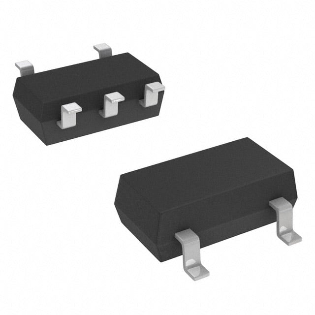
| 供应商器件封装 | SOT-25 |
| 其它名称 | 893-1095-2 |
| 包装 | 带卷 (TR) |
| 安装类型 | 表面贴装 |
| 封装/外壳 | SC-74A,SOT-753 |
| 工作温度 | -40°C ~ 85°C |
| 标准包装 | 3,000 |
| 特色产品 | http://www.digikey.com/product-highlights/cn/zh/torex-xc6221-ldo-voltage-regulators/2431 |
| 电压-跌落(典型值) | 0.16V @ 100mA |
| 电压-输入 | 最高 6V |
| 电压-输出 | 1.5V |
| 电流-输出 | 200mA |
| 电流-限制(最小值) | 200mA |
| 稳压器拓扑 | 正,固定式 |
| 稳压器数 | 1 |


- 商务部:美国ITC正式对集成电路等产品启动337调查
- 曝三星4nm工艺存在良率问题 高通将骁龙8 Gen1或转产台积电
- 太阳诱电将投资9.5亿元在常州建新厂生产MLCC 预计2023年完工
- 英特尔发布欧洲新工厂建设计划 深化IDM 2.0 战略
- 台积电先进制程称霸业界 有大客户加持明年业绩稳了
- 达到5530亿美元!SIA预计今年全球半导体销售额将创下新高
- 英特尔拟将自动驾驶子公司Mobileye上市 估值或超500亿美元
- 三星加码芯片和SET,合并消费电子和移动部门,撤换高东真等 CEO
- 三星电子宣布重大人事变动 还合并消费电子和移动部门
- 海关总署:前11个月进口集成电路产品价值2.52万亿元 增长14.8%


PDF Datasheet 数据手册内容提取
XC6221 Series ETR0328_015 ■GENERAL DESCRIPTION The XC6221 series is a high accuracy, low noise, high speed, low dropout CMOS regulator with high ripple rejection. The series includes a reference voltage source, an error amplifier, a current limiter, and a phase compensation circuit. The CE function enables the entire circuit to be in stand-by state by inputting low level signal. As for the XC6221B/D stand-by mode, the electric charge at the output capacitor (CL) will be discharged by the internal auto-discharge switch, and as a result the V pin quickly returns to the V level. The output stabilization capacitor (C ) is also compatible with low ESR ceramic OUT SS L capacitors. Output voltage is selectable in 0.05V increments within a range of 0.80V~5.00V, using the laser trimming technology set in factory. The current limiter's fold-back circuit also operates as a short circuit protection and an output current limiter at the output pin. The series achieves a fast response with only 25μA of low power consumption. Also the series has low dropout voltage characteristics, which is 80mV at I =100mA and V =3.0V. OUT OUT With the use of small USP-4 and ultra small USPN-4 packages, a small footprint circuit can be designed. ■APPLICATIONS ■FEATURES ●Smart phones / Mobile phones Maximum Output Current : 200mA <Up to 250mA (TYP.)> Dropout Voltage : 80mV@ IOUT=100mA,VOUT=3.0V ●Portable game consoles Operating Voltage Range : 1.6V ~ 6.0V Output Voltage Range : 0.80V~5.00V (0.05V increments) ●Digital still cameras / Camcorders Accuracy : +2% (VOUT >1.50V) (Standard) +30mV (V ≦1.45V) (Standard) OUT +1% (V >2.00V) (High Accuracy) ●Digital audio equipments OUT +20mV (V ≦1.95V) (High Accuracy) OUT Low Power Consumption : 25μA (TYP.) ●Mobile devices / terminals Stand-by Current : Less than 0.1μA High Ripple Rejection : 70dB @ 1kHz CE Function : CE Active High Standby current below 0.1μA C High-Speed Auto-Discharge L (XC6221B/D) CE Pin internally pulled-down (XC6221C/D) Low ESR Capacitor : 1.0μF ceramic capacitor Low Output Noise Operating Ambient Temperature : -40℃~+85℃ Packages : USP-4, SOT-25, SSOT-24 USPN-4 Environmentally Friendly : EU RoHS Compliant, Pb Free ■ TYPICAL APPLICATION CIRCUIT ■TYPICAL PERFORMANCE CHARACTERISTICS ●Load Transient Response XC6221x182 VIN=VCE=2.8V , Tr=Tf=5μs Ta=25℃ , CIN=CL=1.0μF (ceramic) 1.9 300 Output Voltage 1.8 250 Output Voltage: V (V)OUT 111...567 100mA Output Current 112050000 Output Current: I (mA)OUT 1.4 50 10mA 1.3 0 Time: (500μs/div) 1/28
XC6221 Series ■PIN CONFIGURATION V NC OUT V V IN OUT 5 4 4 3 VSS 2 3 CE V 1 4 V OUT IN 1 2 1 2 3 CE V SS V V CE IN SS USP-4 SOT-25 SSOT-24 (BOTTOM VIEW) (TOP VIEW) (TOP VIEW) VSS 2 3 CE *It is recommended that the heat dissipation pad of the USP-4 VOUT1 4 VIN package is soldered by using the reference mount pattern and metal mask pattern for mounting strength. The mount pattern USPN-4 should be electrically opened or connected to the VSS (No.2) (BOTTOM VIEW) pin. ■PIN ASSIGNMENT PIN NUMBER PIN NAME FUNCTIONS USP-4 SOT-25 SSOT-24 USPN-4 4 1 4 4 V Power Input IN 1 5 3 1 V Output OUT 2 2 2 2 V Ground SS 3 3 1 3 CE ON/OFF Control - 4 - - NC No Connection ■CE PIN LOGIC CONDITION PIN NAME DESIGNATOR CONDITIONS H 1.2V≦V ≦6.0V CE CE L VCE≦0.3V * V : CE pin voltage CE 2/28
XC6221 Series ■PIN FUNCTION ASSIGNMENT XC6221A/B (CE no pull-down resistor) CE LEVEL IC OPERATION HIGH ON LOW OFF OPEN Undefined state XC6221C/D (CE pull-down resistor) CE LEVEL IC OPERATION HIGH ON LOW OFF OPEN ■PRODUCT CLASSIFICATION ●Ordering Information XC6221 ①②③④⑤⑥-⑦(*1) DESIGNATOR ITEM SYMBOL DESCRIPTION A No CE pull-down resistor without C auto discharge L B No CE pull-down resistor with C auto discharge L ① Type of Regulator C CE pull-down resistor without C auto discharge L D CE pull-down resistor with C auto discharge L ②③ Output Voltage 08 ~ 50 ex.) V = 3.00V → ② = 3, ③ = 0 OUT +30mV @ 0.80V≦V ≦1.40V OUT When 0.1V steps such as V =0.80V → ②=0, ③=8, ④=2 2 OUT +2% @ V >1.50V OUT When 0.1V steps such as V =3.00V → ②=3, ③=0, ④=2 OUT +30mV @ 0.85V≦V ≦1.45V OUT When 0.05V steps such as V =0.85V → ②=0, ③=8, ④=A A OUT +2% @ V >1.55V OUT ④ Output Accuracy When 0.05V steps such as VOUT=3.05V → ②=3, ③=0, ④=A +20mV @ 0.80V≦V ≦1.90V OUT When 0.1V steps such as V =0.80V → ②=0, ③=8, ④=1 1 OUT +1% @ V >2.00V OUT When 0.1V steps such as V = 3.00V → ②=3, ③=0, ④=1 OUT +20mV @ 0.85V≦V ≦1.95V OUT When 0.05V steps such as V =0.85V → ②=0, ③=8, ④=B B OUT +1% @ V >2.00V OUT When 0.05V steps such as V = 3.05V → ②=3, ③=0, ④=B OUT GR USP-4 (3,000/Reel) GR-G USP-4 (3,000/Reel) MR SOT-25 (3,000/Reel) ⑤⑥-⑦(*1) Packages MR-G SOT-25 (3,000/Reel) (Order Unit) NR SSOT-24 (3,000/Reel) NR-G SSOT-24 (3,000/Reel) 7R-G USPN-4 (5,000/Reel) (*1) The “-G” suffix indicates that the products are Halogen and Antimony free as well as being fully EU RoHS compliant. (*2) The range of the output voltage of USPN-4 package is 1.20V≦V ≦5.00V. OUT 3/28
XC6221 Series ■BLOCK DIAGRAMS ON/OFF ON/OFF CE Control VIN CE Control VIN - Error Current - Error Current CE CE/ Amp Limit CE CE/ Amp Limit each + each + circuit VOUT circuit VOUT R1 R1 Rdischg CE/ R2 R2 RVeofeltraegnece VSS RVeofeltraegnece VSS ●XXCC66222211AAシリ Sースe゙ries ●XXCC66222211BBシリ Sースe゙ries ON/OFF ON/OFF CE Control VIN CE Control VIN R Pull R Pull -down -down - Error Current - Error Current CEeacChE/ + Amp Limit CEeacChE/ + Amp Limit circuit VOUT circuit VOUT R1 R1 Rdischg CE/ R2 R2 RVeofeltraegnece VSS RVeofeltraegnece VSS ●XXCC6622221C1シCリ ーSスe゙ries ●XXCC66222211DシDリ ーSスe゙ries *Diodes inside the circuit are an ESD protection diode and a parasitic diode. ■ABSOLUTE MAXIMUM RATINGS Ta=25℃ PARAMETER SYMBOL RATINGS UNITS Input Voltage V V -0.3 ~ +6.5 V IN SS Output Current I 400(*1) mA OUT Output Voltage V V – 0.3 ~ V + 0.3 V OUT SS IN CE Input Voltage V V – 0.3 ~ +6.5 V CE SS 120 USP-4 1000(PCB mounted)(*2) 250 SOT-25 600(PCB mounted)(*2) Power Dissipation Pd mW 150 SSOT-24 500(PCB mounted)(*2) 100 USPN-4 600(PCB mounted)(*2) Operating Ambient Temperature Topr - 40 ~ + 85 ℃ Storage Temperature Tstg - 55 ~ +125 ℃ *1 I ≦Pd / (V -V ) OUT IN OUT *2 These values are example data which is taken with the PCB mounted. Please refer to pages 21 to 24 for details. 4/28
XC6221 Series ■ELECTRICAL CHARACTERISTICS ●XC6221A/B/C/D series Ta=25℃ PARAMETER SYMBOL CONDITIONS MIN. TYP. MAX. UNITS CIRCUIT x 0.98 x 1.02 1.50V<V V =V , I =10mA Output Voltage V OUT(T), CE IN OUT (*3) V (*3) OUT(E) OUT(T) V ① (Standard) (* 2) -0.03 (*4) +0.03 V <1.45V, V =V , I =10mA OUT(T) CE IN OUT (*3) (*3) x 0.99 x 1.01 2.00V<V , V =V , I =10mA Output Voltage V OUT(T) CE IN OUT (*3) V (*3) OUT(E) OUT(T) V ① (High Accuracy) (* 2) -0.02 (*4) +0.02 V <1.95V, V =V , I =10mA OUT(T) CE IN OUT (*3) (*3) V =V ,V =V +1.0V, Output Current I CE IN IN OUT(T) 200 250 - mA ① OUTMAX 0.80V<V <5.00V OUT(T) Load Regulation (cid:85)V V =V ,0.1mA≦I ≦100mA - 10 40 mV ① OUT CE IN OUT Dropout Voltage (*5) Vdif V =V I =100mA Refer to the voltage chart mV ① CE IN, OUT Supply Current I V =V 、V = V +1.0V - 25 50 μA ② DD CE IN IN OUT(T) Standby Current I V 6.0V, V =V - 0.01 0.10 μA ② STB IN= CE SS V +0.5V≦V ≦6.0V OUT(T) IN Line Regulation ((cid:85)(cid:85)VV・OVUT / ) 1.10V≦VOUT(T), VCE=VIN, IOUT=10mA - 0.01 0.20 %/V ① IN OUT 1.6V≦V ≦6.0V IN V ≦1.05V, V =V I =10mA OUT(T) CE IN, OUT Input Voltage V 1.6 - 6.0 V ① IN Output Voltage (cid:85)VOUT / VCE=VIN, - ±100 - ppm/℃ ① Temperature Characteristics ((cid:85)Topr・VOUT) IOUT=30mA, -40℃<Topr<85℃ V =5.75V +0.5Vp-pAC IN DC 4.75V≦V OUT(T) V =V , I =30mA, f=1kHz CE IN OUT 60 V ={V +1.0}V +0.5Vp-pAC IN OUT(T) DC 4.05V≦V ≦4.70V OUT(T) V =V , I =30mA, f=1kHz Ripple Rejection Rate PSRR CE IN OUT - - dB ③ V ={V +1.0}V +0.5Vp-pAC IN OUT(T) DC 0.85V≦V ≦4.00V OUT(T) V =V , I =30mA, f=1kHz CE IN OUT 70 V =1.85V +0.5Vp-pAC IN DC V =0.80V OUT(T) V =V , I =30mA, f=1kHz CE IN OUT Limit Current I V =V 200 250 - mA ① LIM CE IN V =V V is short-circuited at Short Current I CE IN, OUT - 30 - mA ① SHORT the V level SS CE High Level Voltage V 1.2 - 6.0 V ④ CEH CE Low Level Voltage V - - 0.3 V ④ CEL V =V (XC6221A/B) -0.1 - 0.1 CE High Level Current I CE IN μA ④ CEH V =6.0V (XC6221C/D) 1.03 - 2.37 CE CE Low Level Current I V =V -0.1 - 0.1 μA ④ CEL CE SS CL Auto-Discharge Resistance R V =6.0V, V =4.0V, V =V - 780 - Ω ① (* 8) DCHG IN OUT CE SS NOTE: * 1: Unless otherwise stated regarding input voltage conditions, V =V +1.0V. IN OUT(T) * 2: V = Effective output voltage OUT (E) (The output voltage when an amply stabilized "V +1.0V" is provided at the V pin while maintaining a certain I value.) OUT (T) IN OUT * 3: The relation between V and V is shown in the voltage chart E-0 and E-1. OU T (E) OUT (T) * 4: VOUT (T) = Nominal output voltage * 5: Vdif = {V (*7)-V (*6)} IN1 OUT1 * 6: V is the voltage equal to 98% of the normal output voltage when amply stabilized V +1.0V are input at the V pin. OUT1 OUT (T) IN * 7: V is the input voltage when V appears at the V pin while input voltage is gradually decreased. IN1 OUT1 OUT * 8: For the XC6221B/D series only. The XC6221A/C series discharges by resistors R1 and R2 only as shown in the block diagrams. * 9: For operating supply current of the XC6221C/D, a current through the pull-down resistor should be considered in addition to the supply current value mentioned above. 5/28
XC6221 Series ■OUTPUT VOLTAGE CHART OUTPUT VOLTAGE OUTPUT VOLTAGE NOMINAL (Standard) (High Accuracy) DROPOUT VOLTAGE OUTPUT Vdif V V VOLTAGE OUT(E) OUT(E) (mV) (V) (V) (V) MIN. MAX. MIN. MAX. TYP. MAX. 0.80 0.7700 0.8300 0.7800 0.8200 500 850 0.85 0.8200 0.8800 0.8300 0.8700 0.90 0.8700 0.9300 0.8800 0.9200 410 750 0.95 0.9200 0.9800 0.9300 0.9700 1.00 0.9700 1.0300 0.9800 1.0200 1.05 1.0200 1.0800 1.0300 1.0700 330 650 1.10 1.0700 1.1300 1.0800 1.1200 1.15 1.1200 1.1800 1.1300 1.1700 1.20 1.1700 1.2300 1.1800 1.2200 1.25 1.2200 1.2800 1.2300 1.2700 230 410 1.30 1.2700 1.3300 1.2800 1.3200 1.35 1.3200 1.3800 1.3300 1.3700 1.40 1.3700 1.4300 1.3800 1.4200 200 360 1.45 1.4200 1.4800 1.4300 1.4700 1.50 1.4700 1.5300 1.4800 1.5200 180 290 1.55 1.5200 1.5800 1.5300 1.5700 1.60 1.5700 1.6300 1.5800 1.6200 1.65 1.6200 1.6800 1.6300 1.6700 160 250 1.70 1.6700 1.7300 1.6800 1.7200 1.75 1.7200 1.7800 1.7300 1.770 1.80 1.7700 1.8300 1.7800 1.8200 1.85 1.8200 1.8800 1.8300 1.8700 125 210 1.90 1.8700 1.9300 1.8800 1.9200 1.95 1.9200 1.9800 1.9300 1.9700 2.00 1.9600 2.0400 1.9800 2.0200 2.05 2.0090 2.0910 2.0295 2.0705 2.10 2.0850 2.1420 2.0790 2.1210 2.15 2.1070 2.1930 2.1285 2.1715 2.20 2.1560 2.2440 2.1780 2.2220 115 195 2.25 2.2050 2.2950 2.2275 2.2725 2.30 2.2540 2.3460 2.2770 2.3230 2.35 2.3030 2.3970 2.3265 2.3735 2.40 2.3520 2.4480 2.3760 2.4240 2.45 2.4010 2.4990 2.4255 2.4745 2.50 2.4500 2.5500 2.4750 2.5250 2.55 2.4990 2.6010 2.5245 2.5755 2.60 2.5480 2.6520 2.5740 2.6260 2.65 2.5970 2.7030 2.6235 2.6765 2.70 2.6460 2.7540 2.6730 2.7270 95 170 2.75 2.6950 2.8050 2.7225 2.7775 2.80 2.7440 2.8560 2.7720 2.8280 2.85 2.7930 2.9070 2.8215 2.8785 2.90 2.8420 2.9580 2.8710 2.9290 2.95 2.8910 3.0090 2.9205 2.9795 *The range of the output voltage of USPN-4 package is 1.20V≦V ≦5.00V. OUT(T) 6/28
XC6221 Series ■OUTPUT VOLTAGE CHART (Continued) OUTPUT VOLTAGE OUTPUT VOLTAGE NOMINAL (Standard) (High Accuracy) DROPOUT VOLTAGE OUTPUT Vdif V V VOLTAGE OUT(E) OUT(E) (mV) (V) (V) (V) MIN. MAX. MIN. MAX. TYP. MAX. 3.00 2.9400 3.0600 2.9700 3.0300 3.05 2.8990 3.1100 3.0195 3.0805 3.10 3.0380 3.1620 3.0690 3.1310 3.15 3.0870 3.2130 3.1185 3.1815 3.20 3.1360 3.2640 3.1680 3.2320 3.25 3.1850 3.3150 3.2175 3.2825 3.30 3.2340 3.3660 3.2670 3.3330 3.35 3.2830 3.4170 3.3165 3.3835 3.40 3.3320 3.4680 3.3660 3.4340 3.45 3.3810 3.5190 3.4155 3.4845 3.50 3.4300 3.5700 3.4650 3.5350 3.55 3.4790 3.6210 3.5145 3.5855 3.60 3.5280 3.6720 3.5640 3.6360 3.65 3.5770 3.7230 3.6135 3.6855 3.70 3.6260 3.7740 3.6630 3.7370 3.75 3.6750 3.8250 3.7125 3.7875 3.80 3.7240 3.8760 3.7620 3.8380 3.85 3.7730 3.9270 3.8115 3.8885 3.90 3.8220 3.9780 3.8610 3.9390 3.95 3.8710 4.0290 3.9105 3.9895 4.00 3.9200 4.0800 3.9600 4.0400 80 140 4.05 3.9690 4.1310 4.0095 4.0905 4.10 4.0180 4.1820 4.0590 4.1410 4.15 4.0670 4.2330 4.1085 4.1915 4.20 4.1160 4.2840 4.1580 4.2420 4.25 4.1650 4.3350 4.2075 4.2925 4.30 4.2140 4.3860 4.2570 4.3430 4.35 4.2630 4.4370 4.3065 4.3935 4.40 4.3120 4.4880 4.3560 4.4440 4.45 4.3610 4.5390 4.4055 4.4945 4.50 4.4100 4.5900 4.4550 4.5450 4.55 4.4590 4.6410 4.5045 4.5955 4.60 4.5080 4.6920 4.5540 4.6460 4.65 4.5570 4.7430 4.6035 4.6965 4.70 4.6060 4.7940 4.6530 4.7470 4.75 4.6550 4.8450 4.7025 4.7975 4.80 4.7040 4.8960 4.7520 4.8480 4.85 4.7530 4.9470 4.8015 4.8985 4.90 4.8020 4.9980 4.8510 4.9490 4.95 4.8510 5.0490 4.9005 4.9995 5.00 4.9000 5.1000 4.9500 5.0500 7/28
XC6221 Series ■OPERATIONAL EXPLANATION <Output Voltage Control> The voltage divided by resistors R1 & R2 is compared with the internal reference voltage by the error amplifier. The P-channel MOSFET connected to the VOUT pin, is then driven by the subsequent output signal. The output voltage at the V pin is controlled & stabilized by a system of negative feedback. The current limit circuit and short protect circuit OUT operate in relation to the level of output current. Further, the IC's internal circuitry can be shutdown via the CE pin's signal. CE OCNo/nOtrFoFl VIN - CE CE/ + EArmropr CuLrimreitnt ceiraccuhit VOUT R1 Rdischg CE/ R2 RVefoelrteagnece VSS <Input and Output Capacitors> The XC6221 needs an output capacitor C for phase compensation. Values required for the phase compensation are L shown in the chart below. If a loss of the capacitance happens, the stable phase compensation may not be obtained. Please ensure to use a capacitor which does not depend on bias or temperature too much. For a stable power input, please connect an input capacitor CIN of 1.0μF between the VIN pin and the VSS pin. ●Except USPN-4 OUTPUT VOLTAGE (V) OUTPUT CAPACITOR VALUE 0.80V〜1.15V C ≧4.7μF L 1.20V〜1.35V C ≧2.2μF L 1.40V〜4.00V C ≧1.0μF L 4.05V〜5.00V C ≧2.2μF L ●USPN-4 OUTPUT VOLTAGE (V) OUTPUT CAPACITOR VALUE 1.20V〜4.00V C ≧2.2μF L 4.05V〜5.00V C ≧4.7μF L <C Auto-Discharge Function> L XC6221B/D series can discharge the electric charge in the output capacitor (C ), when a low signal to the CE pin, which L enables the whole IC circuit to be turned off, is inputted via the N-channel transistor and C auto-discharge resistance L (R ) located between the V pin and the V pin (cf. BLOCK DIAGRAM). The C auto-discharge resistance (R ) DCHG OUT SS L DCHG value is set at 780Ω(V =4.0V @ V =6.0V at typical). The discharge time of the output capacitor (C ) is set by the C OUT IN L L auto-discharge resistance (R ) and the output capacitor (C ). By setting the time constant of the C auto-discharge DCHG L L resistance value [R ] and the output capacitor value (C ) as τ(τ=C x R ), the output voltage after discharge via DCHG L L DCHG the N-channel transistor is calculated by the following formula. V = V x e –t/τ, or t=τIn ( V / V ) OUT(E) OUT(E) where V : Output voltage after discharge V : Output voltage OUT (E) t : Discharge time τ: C auto-discharge resistance R ×Output capacitor value C L DCHG L 8/28
XC6221 Series ■OPERATIONAL EXPLANATION (Continued) <Current Limiter, Short-Circuit Protection> The XC6221 series’ fold-back circuit operates as an output current limiter and a short protection circuit for the output pin. When the load current reaches the current limit level, the fixed current limiter circuit operates and output voltage drops. When the output pin is short-circuited to the V pin, the current falls and reaches about 30mA. SS <CE Pin> The XC6221 internal circuitry can be shutdown via the CE pin signal. In shutdown mode, output at the V pin will be OUT pulled down to the V level via R1 & R2. However, with the XC6221B/D series, the C auto-discharge resistor is SS L connected in parallel to R1 and R2 while the power supply is applied to the V pin. Therefore, time until the V pin IN OUT reaches the V level is shorter. For the XC6221A/B, the output voltage becomes unstable, when the CE pin is left SS open. For the XC6221C/D, the output voltage becomes V level because the CE pin is short-circuited to V via an SS SS internal pull-down resistor. However, the CE input current will be increased via a pull-down resistor when the IC operates. If this IC is used with the correct output voltage for the CE pin, the logic is fixed and the IC will operate normally. However, the supply current may increase as a result of shoot-through current in the IC's internal circuitry when a medium voltage is input. ■NOTES ON USE 1. Please use this IC within the stated maximum ratings. For temporary, transitional voltage drop or voltage rising phenomenon, the IC is liable to malfunction should the ratings be exceeded. 2. Where wiring impedance is high, operations may become unstable due to noise and/or phase lag depending on output current. Please wire the input capacitor (C ) and the output capacitor (C ) as close to the IC as possible. IN L 3. Torex places an importance on improving our products and its reliability. However, by any possibility, we would request user fail-safe design and post-aging treatment on system or equipment. 9/28
XC6221 Series ■TEST CIRCUITS Circuit 1: Output Voltage, Output Current, Dropout Voltage, Input/Operating Voltage, Line Regulation, Load Regulation, Current Limit, Short Current, CL Discharge Resistance Circuit 2: Supply Current, Stand-by Current Circuit 3: Ripple Rejection Rate 10/28
XC6221 Series ■TEST CIRCUITS (Continued) Circuit 4: CE “H” “L” Level Voltage, CE “H” “L” Level Current VIN VOUT A CE CIN VSS CL (ceramic) (ceramic) V V V VCE 11/28
XC6221 Series ■TYPICAL PERFORMANCE CHARACTERISTICS (1) Output Voltage vs. Output Current XC6221x182 XC6221x182 V =V , Ta=25℃ V =V =2.8V CE IN IN CE C =C=1.0μF (ceramic) C =C=1.0μF (ceramic) IN L IN L 2.4 2.4 Output Voltage: V(V) OUT 011...628 VIN=1.9V Output Voltage: V (V)OUT 11..28 Ta=25℃ VIN=2.8V 0.6 Ta=-40℃ VIN=6.0V Ta=85℃ 0 0 0 100 200 300 400 0 100 200 300 400 Output Current: I (mA) OUT Output Current: I (mA) OUT XC6221x302 XC6221x302 VCE=VIN , Ta=25℃ VIN=VCE=4.0V 3.5 CIN=CL=1.0μF (ceramic) 3.5 CIN=CL=1.0μF (ceramic) 3 3 V) 2.5 V) 2.5 V (OUT V (OUT e: 2 e: 2 Voltag 1.5 Voltag 1.5 ut ut p p ut 1 VIN=3.1V ut 1 Ta=25℃ O O VIN=4.0V Ta=-40℃ 0.5 VIN=6.0V 0.5 Ta=85℃ 0 0 0 100 200 300 400 0 100 200 300 400 Output Current: IOUT (mA) Output Current: IOUT (mA) (2) Output Voltage vs. Input Voltage XC6221x182 XC6221x182 VCE=VIN , Ta=25℃ VCE=VIN , Ta=25℃ CIN=CL=1.0μF (ceramic) CIN=CL=1.0μF (ceramic) 2 1.9 1.9 1.85 V) V) V (OUT 1.8 V (OUT 1.8 Voltage: 1.7 Voltage: 1.75 Output 1.6 IIOOUUTT==11m0mAA Output 1.7 IIOOUUTT==11m0mAA 1.5 IOUT=30mA 1.65 IOUT=30mA IOUT=100mA IOUT=100mA 1.4 1.6 1 1.5 2 2.5 3 4 4.5 5 5.5 6 Input Voltage: VIN (V) Input Voltage: VIN (V) 12/28
XC6221 Series ■TYPICAL PERFORMANCE CHARACTERISTICS (Continued) (2) Output Voltage vs. Input Voltage (Continued) XC6221x302 XC6221x302 V =V ,Ta=25℃ V =V , Ta=25℃ CE IN CE IN C =C=1.0μF (ceramic) C =C=1.0μF (ceramic) 3.2 IN L 3.1 IN L 3.1 3.05 V) 3 V) Voltage: V (OUT 22..89 Voltage: V (OUT 2.953 Output 2.7 IIOOUUTT==11m0mAA Output 2.9 IIOOUUTT==11m0mAA 2.6 IOUT=30mA 2.85 IOUT=30mA IOUT=100mA IOUT=100mA 2.5 2.8 2 2.5 3 3.5 4 4 4.5 5 5.5 6 Input Voltage: VIN (V) Input Voltage: VIN (V) (3) Dropout Voltage vs. Output Current XC6221x182 XC6221x302 VCE=VIN VCE=VIN 0.4 CIN=CL=1.0μF (ceramic) 0.4 CIN=CL=1.0μF (ceramic) 0.35 Ta=85℃ 0.35 Ta=85℃ Ta=25℃ Dropout Voltage: Vdif (V) 000.0.012...12355 Ta=-40℃ Dropout Voltage: Vdif (V) 000.0.012...15253 TTaa==2-54℃0℃ 0.05 0.05 0 0 0 50 100 150 200 0 50 100 150 200 Output Current: IOUT (mA) Output Current: IOUT (mA) (4) Output Voltage vs. Ambient Temperature XC6221x182 XC6221x302 VIN=VCE=2.8V , IOUT=30mA VIN=VCE=4.0V , IOUT=30mA 1.9 CIN=CL=1.0μF (ceramic) 3.1 CIN=CL=1.0μF (ceramic) Output Voltage: V (V)OUT 11.1.78.585 Output Voltage: V (V)OUT 23..90535 1.7 2.9 -50 -25 0 25 50 75 100 -50 -25 0 25 50 75 100 Ambient Temperature: Topr (℃) Ambient Temperature: Topr (℃) 13/28
XC6221 Series ■TYPICAL PERFORMANCE CHARACTERISTICS (Continued) (5) Supply Current vs. Input Voltage XC6221x182 XC6221x302 70 VCE=VIN , CIN=CL=1.0μF (ceramic) 70 VCE=VIN , CIN=CL=1.0μF (ceramic) 60 Ta=85℃ 60 Ta=85℃ Ta=25℃ Ta=25℃ A) 50 Ta=-40℃ A) 50 Ta=-40℃ Supply Current: I (uSS 234000 Supply Current: I (uSS 234000 10 10 0 0 0 1 2 3 4 5 6 0 1 2 3 4 5 6 Input Voltage: VIN (V) Input Voltage: VIN (V) (6) CL-Discharge Resistance vs. Ambient Temperature XC6221B V =6.0V , V =V , V =4.0V IN CE SS OUT C =C=1.0μF (ceramic) 1200 IN L Ω) (G 1000 H C D ce: R 800 n a st si Re 600 e g char 400 Dis - uto 200 A C L 0 -50 -25 0 25 50 75 100 Ambient Temperature: Topr (℃) (7) Load Transient Response XC6221x182 XC6221x302 VIN=VCE=2.8V , Tr=Tf=5μs VIN=VCE=4.0V , Tr=Tf=5μs 1.9 Ta=25℃ , CIN=CL=1.0μF (ceramic) 300 3.1 Ta=25℃ , CIN=CL=1.0μF (ceramic) 300 Output Voltage Output Voltage 1.8 250 3 250 Output Voltage: V (V)OUT 111...567 100mA Output Current 112050000 Output Current: I (mA)OUT Output Voltage: V (V)OUT 222...789 100mA Output Current 112050000 Output Current: I (mA)OUT 1.4 50 2.6 50 10mA 10mA 1.3 0 2.5 0 Time: (500μs/div) Time: (500μs/div) 14/28
XC6221 Series ■TYPICAL PERFORMANCE CHARACTERISTICS (Continued) (8) Line Transient Response XC6221x182 XC6221x182 V =V , Tr=Tf=5μs VCE=VIN , Tr=Tf=5μs ICE=30INm A , Ta=25℃ , C=1.0μF(ceramic) 5 IOUT=1mA , Ta=25℃ , CL=1.0μF(ceramic) 2 5 OUT L 2 Input Voltage Input Voltage 4 1.95 4 1.95 Input Voltage: V (V)IN 123 Output Voltage 111...8895 Output Voltage: V (V)OUT Input Voltage: V (V)IN 123 Output Voltage 111...8895 Output Voltage: V (V)OUT 0 1.75 0 1.75 -1 1.7 -1 1.7 Time: (20μs/div) Time: (20μs/div) XC6221x182 XC6221x302 VCE=VIN , Tr=Tf=5μs VCE=VIN , Tr=Tf=5μs IOUT=100mA , Ta=25℃ , CL=1.0μF (ceramic) IOUT=1mA , Ta=25℃ , CL=1.0μF (ceramic) 5 2 6 3.2 Input Voltage Input Voltage 4 1.95 5 3.15 Input Voltage: V (V)IN 123 Output Voltage 111...8895 Output Voltage: V (V)OUT Input Voltage: V (V)IN 234 Output Voltage 333..015 Output Voltage: V (V)OUT 0 1.75 1 2.95 -1 1.7 0 2.9 Time: (20μs/div) Time: (20μs/div) XC6221x302 XC6221x302 V =V , Tr=Tf=5μs V =V , Tr=Tf=5μs CE IN CE IN I =30mA , Ta=25℃ , C=1.0μF (ceramic) I =100mA , Ta=25℃ , C=1.0μF (ceramic) 6 OUT L 3.2 6 OUT L 3.2 Input Voltage Input Voltage 5 3.15 5 3.15 V (V)IN 4 3.1 V (V)OUT V (V)IN 4 3.1 V (V)OUT Voltage: 3 3.05 Voltage: Voltage: 3 3.05 Voltage: Input 2 Output Voltage 3 Output Input 2 Output Voltage 3 Output 1 2.95 1 2.95 0 2.9 0 2.9 Time: (20μs/div) Time: (20μs/div) 15/28
XC6221 Series ■TYPICAL PERFORMANCE CHARACTERISTICS (Continued) (9) Input Rise Characteristics XC6221x182xx XC6221x182xx V =V , Tr=5μs V =V , Tr=5μs CE IN CE IN I =1mA , Ta=25℃ , C=1.0μF (ceramic) I =30mA , Ta=25℃ , C=1.0μF (ceramic) OUT L OUT L 4 7 4 7 Input Voltage Input Voltage 3 6 3 6 Input Voltage: V (V)IN -1012 Output Voltage 2345 Output Voltage: V (V)OUT Input Voltage: V (V)IN -1012 Output Voltage 2345 Output Voltage: V (V)OUT -2 1 -2 1 -3 0 -3 0 Time: (40μs/div) Time: (40μs/div) XC6221x182 XC6221x302 VCE=VIN , Tr=5μs VCE=VIN , Tr=5μs IOUT=100mA , Ta=25℃, CL=1.0μF (ceramic) IOUT=1mA, Ta=25℃, CL=1.0μF (ceramic) 4 7 5 8 Input Voltage 3 Input Voltage 6 4 7 3 6 Voltage: V (V)IN 012 345 Voltage: V (V)OUT Voltage: V (V)IN 12 Output Voltage 45 Voltage: V (V)OUT Input -1 Output Voltage 2 Output Input 0 3 Output -1 2 -2 1 -2 1 -3 0 -3 0 Time: (40μs/div) Time: (40μs/div) XC6221x302 XC6221x302 VCE=VIN , Tr=5μs VCE=VIN , Tr=5μs IOUT=30mA , Ta=25℃, CL=1.0μF (ceramic) IOUT=100mA, Ta=25℃, CL=1.0μF (ceramic) 5 8 5 8 Input Voltage Input Voltage 4 7 4 7 3 6 3 6 V (V)IN 2 5 V (V)OUT V (V)IN 2 5 V (V)OUT Voltage: 1 Output Voltage 4 Voltage: Voltage: 1 Output Voltage 4 Voltage: Input 0 3 Output Input 0 3 Output -1 2 -1 2 -2 1 -2 1 -3 0 -3 0 Time: (40μs/div) Time: (40μs/div) 16/28
XC6221 Series ■TYPICAL PERFORMANCE CHARACTERISTICS (Continued) (10) CE Rise Characteristics XC6221x182 XC6221x182 VIN=2.8V, Tr=5μs VIN=2.8V, Tr=5μs 5 IOUT=1mA ,Ta=25℃, CIN=CL=1.0μF (ceramic) 8 5 IOUT=30mA , Ta=25℃, CIN=CL=1.0μF (ceramic) 8 4 7 4 7 CE Input Voltage CE Input Voltage 3 6 3 6 CE Input Voltage: V (V)CE -1012 Output Voltage 2345 Output Voltage: V (V)OUT CE Input Voltage: V (V)CE -1012 Output Voltage 2345 Output Voltage: V (V)OUT -2 1 -2 1 -3 0 -3 0 Time: (40μs/div) Time: (40μs/div) XC6221x182 XC6221x302 VIN=2.8V, Tr=5μs VIN=4.0V, Tr=5μs IOUT=100mA , Ta=25℃, CIN=CL=1.0μF (ceramic) IOUT=1mA, Ta=25℃, CIN=CL=1.0μF (ceramic) 5 8 5 8 CE Input Voltage 4 7 4 7 CE Input Voltage 3 6 3 6 CE Input Voltage: V (V)CE -1012 Output Voltage 2345 Output Voltage: V (V)OUT CE Input Voltage: V (V)CE -1012 Output Voltage 2345 Output Voltage: V (V)OUT -2 1 -2 1 -3 0 -3 0 Time: (40μs/div) Time: (40μs/div) XC6221x302 XC6221x302 VIN=4.0V, Tr=5μs VIN=4.0V, Tr=5μs 5 IOUT=30mA, Ta=25℃, CIN=CL=1.0μF (ceramic) 8 5 IOUT=100mA, Ta=25℃, CIN=CL=1.0μF (ceramic) 8 CE Input Voltage CE Input Voltage 4 7 4 7 3 6 3 6 CE Input Voltage: V (V)CE 012 Output Voltage 345 Output Voltage: V (V)OUT CE Input Voltage: V (V)CE 012 Output Voltage 345 Output Voltage: V (V)OUT -1 2 -1 2 -2 1 -2 1 -3 0 -3 0 Time: (40μs/div) Time: (40μs/div) 17/28
XC6221 Series ■TYPICAL PERFORMANCE CHARACTERISTICS (Continued) (11) Ripple Rejection Rate XC6221x302 XC6221x182 V =V =4.0V +0.5V , V =V =2.8V +0.5V IN CE DC P-PAC IN CE DC P-PAC I =30mA , Ta=25℃ , C=1.0μF (ceramic) I =30mA , Ta=25℃ , C=1.0μF (ceramic) OUT L 80 OUT L 80 70 70 R (dB) 60 R (dB) 60 R R ate: PS 50 ate: PS 50 n R 40 n R 40 Ripple Rejectio 123000 Ripple Rejectio 123000 0 0 0.01 0.1 1 10 100 1000 0.01 0.1 1 10 100 1000 Ripple Frequency: f (kHz) Ripple Frequency: f (kHz) 18/28
XC6221 Series ■PACKAGING INFORMATION ●USP-4 ●SOT-25 (unit : mm) (unit : mm) * Soldering fillet surface is not formed because the sides of the pins are plated. ●SSOT-24 ●USPN-4 (unit : mm) (unit : mm) +0.21.25-0.1 2.1±0.3 +0-0.2 0.3 ±0.1 MAX 0.9 1.1 19/28
XC6221 Series ■ PACKAGING INFORMATION (Continued) ●USP-4 Reference Pattern Layout ●USP-4 Reference Metal Mask Design (unit : mm) (unit : mm) ●USPN-4 Reference Pattern Layout ●USPN-4 Reference Metal Mask Design (unit : mm) (unit : mm) 0.6 0.45 0.25 0.4 20/28
XC6221 Series ■PACKAGING INFORMATION (Continued) ● USP-4 Power Dissipation Power dissipation data for the USP-4 is shown in this page. The value of power dissipation varies with the mount board conditions. Please use this data as one of reference data taken in the described condition. 1. Measurement Condition (Reference data) Condition: Mount on a board Ambient: Natural convection Soldering: Lead (Pb) free Board: Dimensions 40 x 40 mm (1600 mm2 in one side) Copper (Cu) traces occupy 50% of the board area In top and back faces Package heat-sink is tied to the copper traces Material: Glass Epoxy (FR-4) Thickness: 1.6 mm Through-hole: 4 x 0.8 Diameter Evaluation Board (Unit:mm) 2. Power Dissipation vs. Ambient temperature Board Mount (Tj max = 125℃) Ambient Temperature(℃) Power Dissipation Pd(mW) Thermal Resistance (℃/W) 25 1000 100.00 85 400 Pd Vs. Ta 1200 d P 1000 n: o 800 ti a) pW sim 600 s Di( 400 r e w 200 o P 0 25 45 65 85 105 125 AAmmbibeinetn Tte mTpeemrapteurrea t: uTrae (T℃a): (℃) 21/28
XC6221 Series ■PACKAGING INFORMATION (Continued) ● SOT-25 Power Dissipation Power dissipation data for the SOT-25 is shown in this page. The value of power dissipation varies with the mount board conditions. Please use this data as one of reference data taken in the described condition. 1. Measurement Condition (Reference data) Condition : Mount on a board Ambient : Natural convection Soldering : Lead (Pb) free Board : Dimensions 40×40mm(1600mm2 in one side) Copper (Cu) traces occupy 50% of the board area In top and back faces Package heat-sink is tied to the copper traces (Board of SOT-26 is used) Material : Glass Epoxy(FR-4) Thickness : 1.6mm Through-hole : 4 x 0.8 Diameter Evaluation Board (Unit: mm) 2. Power Dissipation vs. Ambient temperature Board Mount (Tj max = 125℃) Ambient Temperature (℃) Power Dissipation Pd (mW) Thermal Resistance (℃/W) 25 600 166.67 85 240 Pd vs Ta 700 ) W 600 m ( d 500 P n o 400 ti a p 300 si s Di 200 r e w 100 o P 0 25 45 65 85 105 125 Ambient Temperature Ta(℃) 22/28
XC6221 Series ■PACKAGING INFORMATION (Continued) ● SSOT-24 Power Dissipation Power dissipation data for the SSOT-24 is shown in this page. The value of power dissipation varies with the mount board conditions. Please use this data as one of reference data taken in the described condition. 1. Measurement Condition (Reference data) 0 Condition : Mount on a board 8.9 40. 2 Ambient : Natural convection Soldering : Lead (Pb) free Board : Dimensions 40×40mm(1600mm2 in one side) Copper (Cu) traces occupy 50% of the board area In top and back faces Package heat-sink is tied to the copper traces 5 Material : Glass Epoxy(FR-4) 2. Thickness : 1.6mm Through-hole : 4 x 0.8 Diameter Evaluation Board (Unit: mm) 2. Power Dissipation vs. Ambient temperature Board Mount (Tj max = 125℃) Ambient Temperature (℃) Power Dissipation Pd (mW) Thermal Resistance (℃/W) 25 500 200.00 85 200 Pd vs Ta 600 500 400 300 200 100 0 25 45 65 85 105 125 Ambient Temperature Ta(℃) 23/28
XC6221 Series ■PACKAGING INFORMATION (Continued) ● USPN-4 Power Dissipation Power dissipation data for the USPN-4 is shown in this page. The value of power dissipation varies with the mount board conditions. Please use this data as one of reference data taken in the described condition. 40.0 2.5 1. Measurement Condition (Reference data) Condition: Mount on a board 28.9 Ambient: Natural convection Soldering: Lead (Pb) free Board: Dimensions 40 x 40 mm (1600 mm2 in one side) Copper (Cu) traces occupy 50% of the front and 50% of the back. The copper area is divided into four block, one block is 12.5% 1.4 54 0.0 of total. 2. 4 The USPN-4 package has for terminals. 8.9 Each terminal connects one copper block in the front and 2 one in the back. Material: Glass Epoxy (FR-4) Thickness: 1.6 mm Through-hole: 4 x 0.8 Diameter Evaluation Board (Unit:mm) 2. Power Dissipation vs. Ambient temperature Board Mount (Tj max = 125℃) Ambient Temperature(℃) Power Dissipation Pd(mW) Thermal Resistance (℃/W) 25 600 166.67 85 240 Pd Vs. Ta 700 d P 600 n: 500 o ti a) 400 pW sim s 300 Di( r 200 e w 100 o P 0 25 45 65 85 105 125 Ambient Temperature: Ta(℃) 24/28
XC6221 Series ■MARKING RULE ●SOT-25 / USP-4 5 4 ① represents product series ① ② ③ ④ ⑤ 1 ① 4 ④ ② MARK PRODUCT SERIES 2 ⑤ ③ 3 3 XC6221A/B***** 1 2 3 0 XC6221C/D***** SOT-25 USP-4 (TOP VIEW) (TOP VIEW) ② represents type of regulator MARK OUTPUT VOLTAGE 0.1V INCREMENTS OUTPUT VOLTAGE 0.05V INCREMENTS PRODUCT SERIES V =0.80〜3.00V V =3.10〜5.00V V =0.85〜3.05V V =3.15〜4.95V OUT OUT OUT OUT V A E L XC6221A/C***** X B F M XC6221B/D***** ③ represents output voltage MARK OUTPUT VOLTAGE (V) MARK OUTPUT VOLTAGE (V) 0 - 3.10 - 3.15 F 1.60 4.60 1.65 4.65 1 - 3.20 - 3.25 H 1.70 4.70 1.75 4.75 2 - 3.30 - 3.35 K 1.80 4.80 1.85 4.85 3 - 3.40 - 3.45 L 1.90 4.90 1.95 4.95 4 - 3.50 - 3.55 M 2.00 5.00 2.05 - 5 - 3.60 - 3.65 N 2.10 - 2.15 - 6 - 3.70 - 3.75 P 2.20 - 2.25 - 7 0.80 3.80 0.85 3.85 R 2.30 - 2.35 - 8 0.90 3.90 0.95 3.95 S 2.40 - 2.45 - 9 1.00 4.00 1.05 4.05 T 2.50 - 2.55 - A 1.10 4.10 1.15 4.15 U 2.60 - 2.65 - B 1.20 4.20 1.25 4.25 V 2.70 - 2.75 - C 1.30 4.30 1.35 4.35 X 2.80 - 2.85 - D 1.40 4.40 1.45 4.45 Y 2.90 - 2.95 - E 1.50 4.50 1.55 4.55 Z 3.00 - 3.05 - ④⑤ represents production lot number 01, …, 09, 10, 11, …99, 0A, …,0Z, 1A, … 9Z, A0, …, Z9, AA, …, ZZ repeated. (G, I, J, O, Q, W excluded) *No character inversion used. 25/28
XC6221 Series ■MARKING RULE (Continued) ●SSOT-24(Without bar) / USPN-4 4 3 ② ④ 1 ③ ① 4 ① ③ 2 ④ ② 3 1 2 SSOT-24 USPN-4 (TOP VIEW) (TOP VIEW) ① represents type of regulator and output voltage range. OUTPUT TYPE OF OUTPUT VOLTAGE MARK REGULATOR VOLTAGE ACCURACY PRODUCT SERIES RANGE(V) 9 A 0.80〜3.00 1/2(0.1VStep) XC6221A081/2**〜XC6221A301/2** D A 3.10〜4.00 1/2(0.1VStep) XC6221A311/2**〜XC6221A401/2** 0 A 4.10〜5.00 1/2(0.1VStep) XC6221A411/2**〜XC6221A501/2** A A 0.85〜3.05 A/B(0.05VStep) XC6221A08A/B**〜XC6221A30A/B** E A 3.15〜3.95 A/B(0.05VStep) XC6221A31A/B**〜XC6221A39A/B** 0 A 4.05〜4.95 A/B(0.05VStep) XC6221A40A/B**〜XC6221A49A/B** B B 0.80〜3.00 1/2(0.1VStep) XC6221B081/2**〜XC6221B301/2** F B 3.10〜4.00 1/2(0.1VStep) XC6221B311/2**〜XC6221B401/2** P B 4.10〜4.80 1/2(0.1VStep) XC6221B411/2**〜XC6221B481/2** U B 4.90〜5.00 1/2(0.1VStep) XC6221B491/2**〜XC6221B501/2** C B 0.85〜3.05 A/B(0.05VStep) XC6221B31A/B**〜XC6221B39A/B** H B 3.15〜3.95 A/B(0.05VStep) XC6221B40A/B**〜XC6221B49A/B** 8 B 4.05〜4.35 A/B(0.05VStep) XC6221B31A/B**〜XC6221B39A/B** H B 4.45〜4.75 A/B(0.05VStep) XC6221B40A/B**〜XC6221B49A/B** Z B 4.85〜4.95 A/B(0.05VStep) XC6221B40A/B**〜XC6221B49A/B** *The range of the output voltage of USPN-4 package is 1.20V≦V ≦5.00V. OUT(T) ② represents output voltage XC6221A***** (0.8〜5.0V) 、XC6221B***** (0.8〜4.0V) XC6221B***** (4.05〜5.0V) MARK OUTPUT VOLTAGE (V) MARK OUTPUT VOLTAGE (V) MARK OUTPUT VOLTAGE (V) 0 - 3.10 - 3.15 F 1.60 4.60 1.65 - 0 4.10 - - - 1 4.20 - - - 1 - 3.20 - 3.25 H 1.70 4.70 1.75 - 2 4.30 - - - 2 - 3.30 - 3.35 K 1.80 4.80 1.85 - 3 4.40 - - - 3 - 3.40 - 3.45 L 1.90 4.90 1.95 - 4 4.50 - - - 4 - 3.50 - 3.55 M 2.00 5.00 2.05 - 5 4.60 - - - 5 - 3.60 - 3.65 N 2.10 - 2.15 4.05 6 4.70 - - - 7 4.80 - - - 6 - 3.70 - 3.75 P 2.20 - 2.25 4.15 8 - - - - 7 0.80 3.80 0.85 3.85 R 2.30 - 2.35 4.25 9 - 4.05 4.45 - 8 0.90 3.90 0.95 3.95 S 2.40 - 2.45 4.35 X 4.90 4.15 4.55 4.85 9 1.00 4.00 1.05 - T 2.50 - 2.55 4.45 Y 5.00 4.25 4.65 4.95 A 1.10 4.10 1.15 - U 2.60 - 2.65 4.55 Z - 4.35 4.75 - B 1.20 4.20 1.25 - V 2.70 - 2.75 4.65 C 1.30 4.30 1.35 - X 2.80 - 2.85 4.75 D 1.40 4.40 1.45 - Y 2.90 - 2.95 7.85 E 1.50 4.50 1.55 - Z 3.00 - 3.05 4.95 ③④ represents production lot number 01, …, 09, 10, 11, …, 99, 0A, …, 0Z, 1A, …, 9Z, A0, …, Z9, AA, …, ZZ repeated. (G, I, J, O, Q, W excluded) *No character inversion used. 26/28
XC6221 Series ■MARKING RULE (Continued) ●SSOT-24(With bar) / USPN-4 4 3 ② ④ ① ③ 1 4 ③ ① 2 ④ ② 3 1 2 SSOT-24 USPN-4 (TOP VIEW) (TOP VIEW) ① represents type of regulator and output voltage range. OUTPUT TYPE OF OUTPUT VOLTAGE MARK REGULATOR VOLTAGE ACCURACY PRODUCT SERIES RANGE(V) 0 C 0.80〜3.70 1/2(0.1VStep) XC6221C081/2**〜XC6221C371/2** 1 C 3.80〜5.00 1/2(0.1VStep) XC6221C381/2**〜XC6221C501/2** 2 C 0.85〜3.75 A/B(0.05VStep) XC6221C08A/B**〜XC6221C37 A/B** 3 C 3.85〜4.95 A/B(0.05VStep) XC6221C38 A/B**〜XC6221C50 A/B** 4 D 0.80〜3.70 1/2(0.1VStep) XC6221D081/2**〜XC6221D371/2** 5 D 3.80〜5.00 1/2(0.1VStep) XC6221D381/2**〜XC6221D501/2** 6 D 0.85〜3.75 A/B(0.05VStep) XC6221D08A/B**〜XC6221D37 A/B** 7 D 3.85〜4.95 A/B(0.05VStep) XC6221D38 A/B**〜XC6221D50 A/B** * The range of the output voltage of USPN-4 package is 1.20V≦V ≦5.00V. OUT(T) ② represents output voltage MARK OUTPUT VOLTAGE (V) MARK OUTPUT VOLTAGE (V) 0 0.80 3.80 0.85 3.85 F 2.30 - 2.35 - 1 0.90 3.90 0.95 3.95 H 2.40 - 2.45 - 2 1.00 4.00 1.05 4.05 K 2.50 - 2.55 - 3 1.10 4.10 1.15 4.15 L 2.60 - 2.65 - 4 1.20 4.20 1.25 4.25 M 2.70 - 2.75 - 5 1.30 4.30 1.35 4.35 N 2.80 - 2.85 - 6 1.40 4.40 1.45 4.45 P 2.90 - 2.95 - 7 1.50 4.50 1.55 4.55 R 3.00 - 3.05 - 8 1.60 4.60 1.65 4.65 S 3.10 - 3.15 - 9 1.70 4.70 1.75 4.75 T 3.20 - 3.25 - A 1.80 4.80 1.85 4.85 U 3.30 - 3.35 - B 1.90 4.90 1.95 4.95 V 3.40 - 3.45 - C 2.00 5.00 2.05 - X 3.50 - 3.55 - D 2.10 - 2.15 - Y 3.60 - 3.65 - E 2.20 - 2.25 - Z 3.70 - 3.75 - ③④ represents production lot number 01, …, 09, 10, 11, …, 99, 0A, …, 0Z, 1A, …, 9Z, A0, …, Z9, AA, …, ZZ repeated. (G, I, J, O, Q, W excluded) *No character inversion used. 27/28
XC6221 Series 1. The products and product specifications contained herein are subject to change without notice to improve performance characteristics. Consult us, or our representatives before use, to confirm that the information in this datasheet is up to date. 2. We assume no responsibility for any infringement of patents, patent rights, or other rights arising from the use of any information and circuitry in this datasheet. 3. Please ensure suitable shipping controls (including fail-safe designs and aging protection) are in force for equipment employing products listed in this datasheet. 4. The products in this datasheet are not developed, designed, or approved for use with such equipment whose failure of malfunction can be reasonably expected to directly endanger the life of, or cause significant injury to, the user. (e.g. Atomic energy; aerospace; transport; combustion and associated safety equipment thereof.) 5. Please use the products listed in this datasheet within the specified ranges. Should you wish to use the products under conditions exceeding the specifications, please consult us or our representatives. 6. We assume no responsibility for damage or loss due to abnormal use. 7. All rights reserved. No part of this datasheet may be copied or reproduced without the prior permission of TOREX SEMICONDUCTOR LTD. 28/28