ICGOO在线商城 > 集成电路(IC) > PMIC - 稳压器 - 线性 > ZLDO1117K12TC
 Datasheet下载
- 型号: ZLDO1117K12TC
- 制造商: Diodes Inc.
- 库位|库存: xxxx|xxxx
- 要求:
| 数量阶梯 | 香港交货 | 国内含税 |
| +xxxx | $xxxx | ¥xxxx |
查看当月历史价格
查看今年历史价格
ZLDO1117K12TC产品简介:
ICGOO电子元器件商城为您提供ZLDO1117K12TC由Diodes Inc.设计生产,在icgoo商城现货销售,并且可以通过原厂、代理商等渠道进行代购。 ZLDO1117K12TC价格参考¥3.46-¥8.10。Diodes Inc.ZLDO1117K12TC封装/规格:PMIC - 稳压器 - 线性, Linear Voltage Regulator IC Positive Fixed 1 Output 1.2V 1A TO-252-3。您可以下载ZLDO1117K12TC参考资料、Datasheet数据手册功能说明书,资料中有ZLDO1117K12TC 详细功能的应用电路图电压和使用方法及教程。
Diodes Incorporated的ZLDO1117K12TC是一款PMIC(电源管理集成电路)中的线性稳压器,其主要应用场景包括以下几个方面:

 1. 便携式电子设备
   - ZLDO1117K12TC具有低功耗和小封装的特点,非常适合用于对能效要求较高的便携式设备,如智能手机、平板电脑、可穿戴设备(智能手表、健康监测器)等。
   - 其1.2V的固定输出电压可以为处理器内核、传感器、无线模块等低电压组件供电。

 2. 嵌入式系统
   - 在工业控制、物联网(IoT)设备和嵌入式计算平台中,该稳压器可用于为核心处理器、微控制器(MCU)、存储器和其他外围电路提供稳定的电源。
   - 它的小尺寸(如SOT-23封装)和高精度输出电压特性使其成为紧凑型设计的理想选择。

 3. 通信设备
   - ZLDO1117K12TC适用于路由器、调制解调器、无线接入点等通信设备中的低噪声电源需求。
   - 其出色的纹波抑制比(PSRR)能够减少干扰,确保信号完整性,特别适合射频(RF)和模拟电路部分。

 4. 消费类电子产品
   - 包括数码相机、游戏机手柄、蓝牙音箱等在内的消费类电子产品需要稳定且高效的电源解决方案,这款线性稳压器能够满足这些需求。
   - 它的简单设计和易于使用特性降低了整体开发成本。

 5. 医疗电子设备
   - 在便携式医疗设备(如血糖仪、脉搏血氧仪)中,ZLDO1117K12TC提供了可靠且低功耗的电源支持,同时其稳定性有助于提高测量精度。

 6. 汽车电子
   - 虽然ZLDO1117K12TC并非专门针对汽车级应用设计,但在某些非关键领域(如信息娱乐系统或车内照明控制)中,它仍然可以发挥作用。

总结来说,ZLDO1117K12TC凭借其高效、稳定和紧凑的设计,广泛应用于需要低电压、低功耗及高精度电源供应的各种场景。
| 参数 | 数值 |
| 产品目录 | 集成电路 (IC)半导体 |
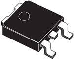
| 描述 | IC REG LDO 1.2V 1A TO252-3低压差稳压器 LDO Regulator IC 1.2V,1A |
| 产品分类 | |
| 品牌 | Diodes Incorporated |
| 产品手册 | |
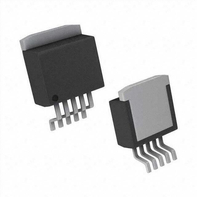
| 产品图片 |
|
| rohs | 符合RoHS无铅 / 符合限制有害物质指令(RoHS)规范要求 |
| 产品系列 | 电源管理 IC,低压差稳压器,Diodes Incorporated ZLDO1117K12TC- |
| 数据手册 | |
| 产品型号 | ZLDO1117K12TC |
| PCN设计/规格 | |
| RoHS指令信息 | http://diodes.com/download/4349 |
| 产品目录页面 | |
| 产品种类 | 低压差稳压器 |
| 供应商器件封装 | TO-252-3 |
| 其它名称 | ZLDO1117K12DICT |
| 包装 | 剪切带 (CT) |
| 参考电压 | 1.2 V |
| 商标 | Diodes Incorporated |
| 回动电压—最大值 | 1.3 V |
| 安装类型 | 表面贴装 |
| 安装风格 | SMD/SMT |
| 封装 | Reel |
| 封装/外壳 | TO-252-3,DPak(2 引线+接片),SC-63 |
| 封装/箱体 | TO-252-3L |
| 工作温度 | -40°C ~ 125°C |
| 最大工作温度 | + 125 C |
| 最大输入电压 | 18 V |
| 最小工作温度 | - 40 C |
| 标准包装 | 1 |
| 电压-跌落(典型值) | 1.11V @ 1A |
| 电压-输入 | 2.7 V ~ 18 V |
| 电压-输出 | 1.2V |
| 电流-输出 | 1A |
| 电流-限制(最小值) | 1.1A |
| 稳压器拓扑 | 正,固定式 |
| 稳压器数 | 1 |
| 线路调整率 | 0.2 % |
| 负载调节 | 0.2 % |
| 输出电压 | 1.2 V |
| 输出电压容差 | 2 % |
| 输出电流 | 1 A |
| 输出端数量 | 1 Output |
| 输出类型 | Fixed |


- 商务部:美国ITC正式对集成电路等产品启动337调查
- 曝三星4nm工艺存在良率问题 高通将骁龙8 Gen1或转产台积电
- 太阳诱电将投资9.5亿元在常州建新厂生产MLCC 预计2023年完工
- 英特尔发布欧洲新工厂建设计划 深化IDM 2.0 战略
- 台积电先进制程称霸业界 有大客户加持明年业绩稳了
- 达到5530亿美元!SIA预计今年全球半导体销售额将创下新高
- 英特尔拟将自动驾驶子公司Mobileye上市 估值或超500亿美元
- 三星加码芯片和SET,合并消费电子和移动部门,撤换高东真等 CEO
- 三星电子宣布重大人事变动 还合并消费电子和移动部门
- 海关总署:前11个月进口集成电路产品价值2.52万亿元 增长14.8%


PDF Datasheet 数据手册内容提取
A Product Line of Diodes Incorporated ZLDO1117 1A LOW DROPOUT POSITIVE REGULATOR 1.2V, 1.5V, 1.8V, 2.5V, 3.3V, 5.0V AND ADJUSTABLE OUTPUTS Description Pin Assignments ZLDO1117 is a low dropout positive adjustable or fixed-mode SOT223 regulator with 1A output current capability. The ZLDO1117 has a 2% tolerance across the industrial temperature range and is guaranteed to have lower than 1.2V dropout at full load current making it ideal to provide well-regulated outputs of 1.2V to 5.0V with input supply voltages up to 18V. The ZLDO1117 is ideally suited to provide well-regulated supplies for low voltage IC applications such as high-speed bus termination and low current 3.3V logic supply across the whole industrial temperature range. TO252 (Top View) Features 3 Vin • 1.2V Maximum Dropout at Full Load Current 2 Vout • 2% Tolerance Over Temperature, Line and Load Variations 1 Adj (GND) • Fast Transient Response Tab is Vout • Output Current Limiting • Built-in Thermal Shutdown • Good Noise Rejection • Suitable for use with MLCC Capacitors • Qualified to AEC-Q100 Grade 2 (see ‘Ordering Information’) • PPAP capable (Note 4) • -40 to +125°C Junction Temperature Range • Available in TO252 and SOT223 with “Green” Molding Compound (No Br, Sb) (cid:131) Lead-Free Finish; RoHS Compliant (Notes 1 & 2) (cid:131) Halogen and Antimony Free. “Green” Device (Note 3) Notes: 1. EU Directive 2002/95/EC (RoHS) & 2011/65/EU (RoHS 2) compliant. All applicable RoHS exemptions applied. 2. See http://www.diodes.com for more information about Diodes Incorporated’s definitions of Halogen- and Antimony-free, "Green" and Lead-free. 3. Halogen- and Antimony-free "Green” products are defined as those which contain <900ppm bromine, <900ppm chlorine (<1500ppm total Br + Cl) and <1000ppm antimony compounds. 4. Automotive products are AEC-Q100 qualified and are PPAP capable. Automotive, AEC-Q100 and standard products are electrically and thermally the same, except where specified. Typical Applications Circuit 1A I/O – 1.8V Core Regulator ZLDO1117-18 3.3V 1.8V 4.7µF MLCC 4.7µF MLCC ZLDO1117 1 of 14 July 2012 Document number: DS32018 Rev. 6 - 2 www.diodes.com © Diodes Incorporated
A Product Line of Diodes Incorporated ZLDO1117 Pin Descriptions Pin Pin I/O Function Name Number A resistor divider from this pin to the V pin and ground sets the output voltage (Ground only for Adj (GND) I 1 OUT Fixed-Mode). The output of the regulator. A minimum of 4.7µF capacitor (0.05Ω ≤ ESR ≤ 0.5Ω) must be connected V O 2 from this pin to ground to insure stability. For improved ac load response a larger output capacitor is OUT recommended. The input pin of regulator. Typically a large storage capacitor (0.05Ω ≤ ESR ≤ 0.5Ω) is connected from this pin to ground to ensure that the input voltage does not sag below the minimum dropout voltage V I 3 IN during the load transient response. This pin must always be 1.3V higher than V in order for the OUT device to regulate properly. Absolute Maximum Ratings (@TA = +25°C, unless otherwise specified.) Symbol Parameter Rating Unit V Input Supply Voltage (Relative to Ground) -0.03 to +18 V IN T Junction Temperature +150 °C J Power Dissipation See SOA Curve T Storage Temperature -65 to +150 °C ST Unless otherwise stated voltages specified are relative to the ANODE pin. 1.2 1 0.8 A) (OAD0.6 IL SOA 0.4 0.2 0 0 5 10 15 20 25 VIN - VOUT (V) Safe Operation Area (SOA) Curve ESD Susceptibility Symbol Parameter Rating Unit HBM Human Body Model 4 kV MM Machine Model 400 V Stresses greater than the 'Absolute Maximum Ratings' specified above, may cause permanent damage to the device. These are stress ratings only; functional operation of the device at these or any other conditions exceeding those indicated in this specification is not implied. Device reliability may be affected by exposure to absolute maximum rating conditions for extended periods of time. Semiconductor devices are ESD sensitive and may be damaged by exposure to ESD events. Suitable ESD precautions should be taken when handling and transporting these devices ZLDO1117 2 of 14 July 2012 Document number: DS32018 Rev. 6 - 2 www.diodes.com © Diodes Incorporated
A Product Line of Diodes Incorporated ZLDO1117 Recommended Operating Conditions (@TA = +25°C, unless otherwise specified.) Symbol Parameter Min Max Unit V Input voltage 2.7 (Note 8) 18 V IN I Output current 0.01 1 A O T Operating Junction Temperature Range (Note 5) -40 +125 °C J Package Thermal Data Thermal Resistance Package Rating Unit SOT223 (Note 6) 107 Junction-to-Ambient, θ °C/W JA TO252 (Note 7) 73 SOT223 (Note 6) 16 Junction-to-Case, θ °C/W JC TO252 (Note 7) 12 Notes: 5. ZLDO1117 contains an internal thermal limiting circuit that is designed to protect the regulator in the event that the maximum junction temperature exceeded. When activated, typically at 150°C, the regulator Output switches off and then back on as the die cools. 6. Test condition for SOT223: T = +27°C, no air flow, device mounted on 2”X2” polyimide PCB, 2 oz copper, 5.6mmX5.6mm pad. A 7. Test condition for TO252: T = +27°C, no air flow, device mounted on 2”X2” polyimide PCB, 1 oz copper, 2cmX2cm pad. A 8. Ensures correct operation without entering dropout. Device will continue to operate below this minimum input voltage under dropout conditions. Electrical Characteristics (@TA = +25°C, unless otherwise specified.) Parameter Conditions T Min Typ Max Unit A (V -V ) = 2V, I = 10mA 25 1.238 1.250 1.263 IN OUT O Reference Voltage ZLDO1117-ADJ V +1.4V < V < 10V, V OUT IN FT 1.225 1.275 10mA < I < 1A O I = 10mA, V = 3.2V 25 1.188 1.200 1.212 V ZLDO1117-1.2 O IN 10mA< I < 1A, 2.7V <V < 12V FT 1.176 1.224 O IN I = 10mA, V = 3.5V 25 1.485 1.500 1.515 ZLDO1117-1.5 O IN V 0 < I < 1A, 2.9V <V < 12V FT 1.470 1.530 O IN I = 10mA, V = 3.8V 25 1.782 1.800 1.818 ZLDO1117-1.8 O IN V 0 < I < 1A, 3.2V <V < 12V FT 1.764 1.836 Output Voltage O IN I = 10mA, V = 4.5V 25 2.475 2.500 2.525 ZLDO1117-2.5 O IN V 0 < I < 1A, 3.9V <V < 12V FT 2.450 2.550 O IN I = 10mA, V = 5.3V 25 3.267 3.300 3.333 ZLDO1117-3.3 O IN V 0 < I < 1A, 4.7V <V < 12V FT 3.235 3.365 O IN I = 10mA, V = 7V 25 4.95 5.000 5.05 ZLDO1117-5.0 O IN V 0 < I < 1A, 6.4V <V < 12V FT 4.900 5.100 O IN ZLDO1117-ADJ I = 10mA, 25 0.1 O % ZLDO1117-1.2 VOUT+1.5V<VIN<12V FT 0.2 Line Regulation I = 0mA, 25 0.1 ZLDO1117-xx O % VOUT+1.5V<VIN<12V FT 0.2 Notes: 9. See thermal regulation specifications for changes in output voltage due to heating effects. Line and load regulation are measured at a constant junction temperature by low duty cycle pulse testing. Load regulation is measured at the output lead = 1/18” from the package. 10. Line and load regulation are guaranteed up to the maximum power dissipation of 15W. Power dissipation is determined by the difference between input and output differential and the output current. Guaranteed maximum power dissipation will not be available over the full input/output range. ZLDO1117 3 of 14 July 2012 Document number: DS32018 Rev. 6 - 2 www.diodes.com © Diodes Incorporated
A Product Line of Diodes Incorporated ZLDO1117 Electrical Characteristics (cont.) (@TA = +25°C, unless otherwise specified.) Parameter Conditions T Min Typ Max Unit A V =3.3V,V =0, 10mA<I <1A, 25 0.2 ZLDO1117-ADJ IN ADJ O % (Notes 9, 10) FT 0.4 V =2.7V, 10mA < I < 1A, 25 0.2 % ZLDO1117-1.2 IN O (Notes 9, 10) FT 0.4 V = 3V, 0 < I < 1A, 25 3 ZLDO1117-1.5 IN O mV (Notes 9, 10) FT 6 V = 3.3V, 0 < I < 1A, 25 4 Load Regulation ZLDO1117-1.8 IN O mV (Notes 9, 10) FT 8 V = 4V, 0 < I < 1A, 25 5 ZLDO1117-2.5 IN O mV (Notes 9, 10) FT 10 V = 4.8V, 0 < I < 1A, 25 6.6 ZLDO1117-3.3 IN O mV (Notes 9, 10) FT 13 V = 6.5V, 0 < I < 1A, 25 10 ZLDO1117-5.0 IN O mV (Notes 9, 10) FT 20 ZLDO1117- 25 1.11 1.2 Dropout Voltage ADJ/1.2/1.5/1.8/2.5/ I = 1A, ΔV = 1%V 0 ~ 125 1.3 V (V -V ) O OUT OUT IN OUT 3.3/5.0 FT 1.35 ZLDO1117- 25 Current Limit ADJ/1.2/1.5/1.8/2.5/ (V -V ) = 5V A IN OUT 3.3/5.0 FT 1. 1 Minimum Load Current ZLDO1117-ADJ V = <18V FT 2 5 mA (Note 8) ZLDO1117-1.2 IN Quiescent current ZLDO1117-xx VIN< 18V, IO = 0mA FT 4 10 mA ZLDO1117-ADJ GND current V = 7V FT 35 120 µA ZLDO1117-1.2 IN Thermal Regulation 30ms pulse 25 0.1 %/W f = 120Hz, C = 25µF Tantalum, Ripple Rejection OUT 25 60 80 dB I = 100mA, ZLDO1117-XXX V = V +3V OUT IN OUT Temperature Stability I = 10mA 0.5 % O Notes: 8. See thermal regulation specifications for changes in output voltage due to heating effects. Line and load regulation are measured at a constant junctiontemperature by low duty cycle pulse testing. Load regulation is measured at the output lead = 1/18” from the package. 9. Line and load regulation are guaranteed up to the maximum power dissipation of 15W. Power dissipation is determined by the difference between input and output differential and the output current. Guaranteed maximum power dissipation will not be available over the full input/output range. ZLDO1117 4 of 14 July 2012 Document number: DS32018 Rev. 6 - 2 www.diodes.com © Diodes Incorporated
A Product Line of Diodes Incorporated ZLDO1117 Typical Characteristics 0.5 0.06 0.4 Adjustable version 0.05 0.3 ILOAD = 10mA 0.2 %)0.04 VOUT+1.5V<VIN<12V, IOUT=10mA Vout (%) 0.01 gulation (0.03 ∆-0.1 Re0.02 e -0.2 Lin0.01 -0.3 -0.4 0 -0.5 -40 -25 -10 5 20 35 50 65 80 95 110 125 -0.01 Temperature (°C) -50 -25 0 25 50 75 100 125 Temperature (C) Output Voltage Variation vs. Temperature Line Regulation vs. Temperature 0.25 1.4 1.3 %) 0.2 VIN=3.3V, 10mA<IOUT<1A V)1.2 ∆VOUTT J= = 1 2%5 ºoCf VOUT Load Regulation (00.1.15 Dropout voltage (01..191 0.8 0.05 0.7 0 0.6 -50 -25 0 25 50 75 100 125 0 0.2 0.4 0.6 0.8 1 Temperature (°C) IOUT (A) Load Regulation vs. Temperature Drop-Out Voltage vs. Current Dropout vs Temperature 70 1.4 60 1.3 50 Dropout (V)11..12 ∆VOUTI O=U 1T=%1 Aof VOUT I (µA)ADJ3400 1 20 0.9 10 0 0.8 -50 -25 0 25 50 75 100 125 -50 -25 0 25 50 75 100 125 Temperature (°C) Temperature (°C) Drop-Out Voltage vs. Temperature Adjust Pin Input Current ZLDO1117 5 of 14 July 2012 Document number: DS32018 Rev. 6 - 2 www.diodes.com © Diodes Incorporated
A Product Line of Diodes Incorporated ZLDO1117 Typical Characteristics ZLDO1117-2.5V ZLDO1117-2.5V CIN = 1µF, COUT = 10µFTANT CIN = 1µF, COUT = 4.7µF MLCC IPRELOAD = 100mA, Istep = 500mA IPRELOAD = 100mA, ISTEP = 500mA 10mV 10mV 0 0 -10mV -10mV 600mA 600mA 100mA 100mA Transient Load Regulation with 10µF Tantalum Transient Load Regulation with 4.7µF MLCC Capacitor Capacitor ZLDO1117 2.5V C = 1µF, C = 4.7µF MLCC IN OUT I = 100mA LOAD 10 0 5V 4V 10µs/div Transient Line Regulation with 4.7µF MLCC Capacitor 90 85 80 B) d on (75 ILOAD = 100mA, VIN - VOUT = 3V ecti70 ej R ple 65 p Ri60 55 50 10 100 1,000 10,000 100,000 Frequency (Hz) Ripple Rejection ZLDO1117 6 of 14 July 2012 Document number: DS32018 Rev. 6 - 2 www.diodes.com © Diodes Incorporated
A Product Line of Diodes Incorporated ZLDO1117 Application Information The ZLDO1117 family of quasi-LDO regulators is easy to use. They are protected against short circuit and thermal overloads. (see block diagram). Thermal protection circuitry will shut down the regulator should the junction temperature exceed +150°C at the sense point. The ZLDO1117 is pin compatible with similar ‘1117 regulators and offers extended temperature range and improved regulation specifications. Operation The ZLDO1117 develops a 1.25V reference voltage between the output and the adjust terminal (see block diagram). By placing a resistor between these two terminals, a constant current is caused to flow through R1 and down through R2. For fixed output variants Resistors R1 and R2 are internal. Stability The ZLDO1117 requires an output capacitor as part of the device frequency compensation. As part of its improved performance over industry standard 1117 the ZLDO1117 is suitable for use with MLCC (Multi Layer Ceramic Chip) capacitors. A minimum of 4.7µF ceramic X7R, 4.7µF tantalum, or 47 µF of aluminum electrolytic is required. The ESR of the output capacitor should be less than 0.5Ω. Surface mount tantalum capacitors, which have very low ESR, are available from several manufacturers. When using MLCC capacitors avoid the use of Y5V dielectrics. Load Regulation For improved load regulation the ZLDO1117-ADJ should have the upper feedback resistor, R, connected as close as possible to V and the 1 OUT lower resistor, R2, connected as close as possible to the load GND return. This helps reduce any parasitic resistance in series with the load. Thermal Considerations ZLDO1117 series regulators have internal thermal limiting circuitry designed to protect the device during overload conditions. For continuous normal load conditions however, the maximum junction temperature rating of +125°C must not be exceeded. It is important to give careful consideration to all sources of thermal resistance from junction to ambient. For the SOT223-3L and TO252-3L packages, which are designed to be surface mounted, additional heat sources mounted near the device must also be considered. Heat sinking is accomplished using the heat spreading capability of the PCB and its copper traces. The θ (junction to tab)of the TO252-3L and SOT223-3L are JC +12°C/W and +16°C/W respectively. Thermal resistances from tab to ambient can be as low as +30°C/W. The total thermal resistance from junction to ambient can be as low as +42 to +46°C/W. This requires a reasonable sized PCB with at least one layer of copper to spread the heat across the board and couple it into the surrounding air. Datasheet specifications using 2 oz copper and a 5mmx5mm pad with T = +27°C, no air flow yielded θ (junction to tab) of A JA +73°C/W and +107°C/W for TO252-3L and SOT223-3L respectively. The thermal resistance for each application will be affected by thermal interactions with other components on the board. Some experimentation will be necessary to determine the actual value. Ripple Rejection When using the ZLDO1117 adjustable device the adjust terminal can be bypassed to improve ripple rejection. When the adjust terminal is bypassed the required value of the output capacitor increases. The device will require an output capacitor of 22µF tantalum or 150µF aluminum electrolytic when the adjust pin is bypassed. Normally, capacitor values on the order of 100µF are used in the output of many regulators to ensure good load transient response with large load current changes. Output capacitance can be increased without limit and larger values of output capacitance further improve stability and transient response. The curves for Ripple Rejection were generated using an adjustable device with the adjust pin bypassed. These curves will hold true for all values of output voltage. For proper bypassing, and ripple rejection approaching the values shown, the impedance of the adjust pin capacitor, at the ripple frequency, should be < R1. R1 is normally in the range of 100Ω to 200Ω. The size of the required adjust pin capacitor is a function of the input ripple frequency. At 120Hz, with R1 = 100Ω, the adjust pin capacitor should be >13µF. At 10kHz only 0.16µF is needed. For fixed voltage devices, and adjustable devices without an adjust pin capacitor, the output ripple will increase as the ratio of the output voltage to the reference voltage (V /V ). For example, with the output voltage equal to 5V, the output ripple will be increased by the ratio of 5V/1.25V. OUT REF It will increase by a factor of four. Ripple rejection will be degraded by 12dB from the value shown on the curve. ZLDO1117 7 of 14 July 2012 Document number: DS32018 Rev. 6 - 2 www.diodes.com © Diodes Incorporated
A Product Line of Diodes Incorporated ZLDO1117 Typical Application Circuits Using ⎧ R2⎫ VOUT =1.25•⎨1+ ⎬ ⎩ R1⎭ then the output voltage becomes: ⎧ 330⎫ VOUT =1.25•⎨1+ ⎬=5.0V ⎩ 110⎭ Figure 1 Basic Adjustable Regulator with 5V Output Figure 2 Adjustable Regulator with IADJ Errors ⎧ R2⎫ VOUT =1.25•⎨1+ ⎬+IADJ•R2 ⎩ R1⎭ Because I typically is 55μA, its effect is negligible in most applications. ADJ VOUT =1.25•⎨⎧1+330 +55•10−6•330⎬⎫=5.02V ~ 0.4% ⎩ 110 ⎭ A. Output capacitor selection is critical for regulator stability. Larger C values benefit the regulator by improving transient response and loop out stability. B. C can be used to improve ripple rejection. If C is used, a C that is larger in value than C must be used. ADJ ADJ out ADJ C. C is recommended if ZLDO1117 is not located near the power supply filter. in D. An external diode is recommended to protect the regulator if the input instantaneously is shorted to GND. E. This device is designed to be stable with tantalum and MLCC capacitors with an ESR less than 0.47Ω. ZLDO1117 8 of 14 July 2012 Document number: DS32018 Rev. 6 - 2 www.diodes.com © Diodes Incorporated
A Product Line of Diodes Incorporated ZLDO1117 Other Application Circuits Figure 3 ZLDO1117 with Extended Output Voltage ZLDO1117 V V IN OUT IN OUT R1 ADJ 121Ω 1% C1 C2 10 F 100 F TTL T1 R2 MMBT3904 365Ω R3 R4 1% 1k 1k Figure 4 ZLDO1117 with Disable Function ZLDO1117x50 AC IN OUT IN ADJ C1 C2 10 F 100 F VOUT = -5V Figure 5 ZLDO1117 as a Negative LDO ZLDO1117 9 of 14 July 2012 Document number: DS32018 Rev. 6 - 2 www.diodes.com © Diodes Incorporated
A Product Line of Diodes Incorporated ZLDO1117 Ordering Information Packaging Part Number Output Voltage Status Reel Quantity Tape width Reel size (Note 11) ZLDO1117KTC TO252 Active 2500 16 mm 13” Adjustable ZLDO1117GTA SOT223 Active 1000 12 mm 7” ZLDO1117K12TC TO252 Active 2500 16 mm 13” 1.2V ZLDO1117G12TA SOT223 Active 1000 12 mm 7” ZLDO1117K15TC TO252 Active 2500 16 mm 13” 1.5V ZLDO1117G15TA SOT223 Active 1000 12 mm 7” ZLDO1117K18TC TO252 Active 2500 16 mm 13” 1.8V ZLDO1117G18TA SOT223 Active 1000 12 mm 7” ZLDO1117K25TC TO252 Active 2500 16 mm 13” 2.5V ZLDO1117G25TA SOT223 Active 1000 12 mm 7” ZLDO1117K33TC TO252 Active 2500 16 mm 13” 3.3V ZLDO1117G33TA SOT223 Active 1000 12 mm 7” ZLDO1117K50TC TO252 Active 2500 16 mm 13” 5.0V ZLDO1117G50TA SOT223 Active 1000 12 mm 7” ZLDO1117QKTC TO252 Active 2500 16 mm 13” Adjustable ZLDO1117QGTA SOT223 Active 1000 12 mm 7” ZLDO1117QK12TC TO252 Active 2500 16 mm 13” 1.2V ZLDO1117QG12TA SOT223 Active 1000 12 mm 7” ZLDO1117QK15TC TO252 Active 2500 16 mm 13” 1.5V ZLDO1117QG15TA SOT223 Active 1000 12 mm 7” ZLDO1117QK18TC TO252 Active 2500 16 mm 13” 1.8V ZLDO1117QG18TA SOT223 Active 1000 12 mm 7” ZLDO1117QK25TC TO252 Active 2500 16 mm 13” 2.5V ZLDO1117QG25TA SOT223 Active 1000 12 mm 7” ZLDO1117QK33TC TO252 Active 2500 16 mm 13” 3.3V ZLDO1117QG33TA SOT223 Active 1000 12 mm 7” ZLDO1117QK50TC TO252 Active 2500 16 mm 13” 5.0V ZLDO1117QG50TA SOT223 Active 1000 12 mm 7” Note: 11. Pad layout as shown on Diodes Inc. suggested pad layout document AP02001, which can be found on our website at http://www.diodes.com/datasheets/ap02001.pdf. ZLDO1117 10 of 14 July 2012 Document number: DS32018 Rev. 6 - 2 www.diodes.com © Diodes Incorporated
A Productt Line of DDiodes Incorrporated ZLLDO1117 Marking Innformationn TO252 SOT223 ZLDO1117 11 of 14 July 20122 Document numberr: DS32018 Rev. 6 - 2 wwww.diodes.com © Diodes Incorporateed
A Product Line of Diodes Incorporated ZLDO1117 Package Outline Dimensions (All dimensions in mm.) SOT223 SOT223 Dim Min Max Typ A 1.55 1.65 1.60 A1 0.010 0.15 0.05 b1 2.90 3.10 3.00 b2 0.60 0.80 0.70 C 0.20 0.30 0.25 D 6.45 6.55 6.50 E 3.45 3.55 3.50 E1 6.90 7.10 7.00 e — — 4.60 e1 — — 2.30 L 0.85 1.05 0.95 Q 0.84 0.94 0.89 All Dimensions in mm A A1 TO252 TO252 Dim Min Max Typ E A A 2.19 2.39 2.29 b3 c2 A1 0.00 0.13 0.08 A2 0.97 1.17 1.07 L3 b 0.64 0.88 0.783 b2 0.76 1.14 0.95 E1 b3 5.21 5.46 5.33 A2 c2 0.45 0.58 0.531 D H D 6.00 6.20 6.10 D1 5.21 − − e − − 2.286 E 6.45 6.70 6.58 L4 A1 E1 4.32 − − H 9.40 10.41 9.91 L L 1.40 1.78 1.59 e L3 0.88 1.27 1.08 2X b2 3X b a L4 0.64 1.02 0.83 a 0° 10° − All Dimensions in mm ZLDO1117 12 of 14 July 2012 Document number: DS32018 Rev. 6 - 2 www.diodes.com © Diodes Incorporated
A Product Line of Diodes Incorporated ZLDO1117 Suggested Pad Layout SOT223 X1 Dimensions Value (in mm) Y1 X1 3.3 X2 1.2 Y1 1.6 C1 Y2 1.6 C1 6.4 C2 2.3 Y2 C2 X2 TO252 X2 Dimensions Value (in mm) Z 11.6 Y2 X1 1.5 X2 7.0 Z Y1 2.5 C Y2 7.0 C 6.9 Y1 E1 2.3 X1 E1 ZLDO1117 13 of 14 July 2012 Document number: DS32018 Rev. 6 - 2 www.diodes.com © Diodes Incorporated
A Product Line of Diodes Incorporated ZLDO1117 IMPORTANT NOTICE DIODES INCORPORATED MAKES NO WARRANTY OF ANY KIND, EXPRESS OR IMPLIED, WITH REGARDS TO THIS DOCUMENT, INCLUDING, BUT NOT LIMITED TO, THE IMPLIED WARRANTIES OF MERCHANTABILITY AND FITNESS FOR A PARTICULAR PURPOSE (AND THEIR EQUIVALENTS UNDER THE LAWS OF ANY JURISDICTION). Diodes Incorporated and its subsidiaries reserve the right to make modifications, enhancements, improvements, corrections or other changes without further notice to this document and any product described herein. Diodes Incorporated does not assume any liability arising out of the application or use of this document or any product described herein; neither does Diodes Incorporated convey any license under its patent or trademark rights, nor the rights of others. Any Customer or user of this document or products described herein in such applications shall assume all risks of such use and will agree to hold Diodes Incorporated and all the companies whose products are represented on Diodes Incorporated website, harmless against all damages. Diodes Incorporated does not warrant or accept any liability whatsoever in respect of any products purchased through unauthorized sales channel. Should Customers purchase or use Diodes Incorporated products for any unintended or unauthorized application, Customers shall indemnify and hold Diodes Incorporated and its representatives harmless against all claims, damages, expenses, and attorney fees arising out of, directly or indirectly, any claim of personal injury or death associated with such unintended or unauthorized application. Products described herein may be covered by one or more United States, international or foreign patents pending. Product names and markings noted herein may also be covered by one or more United States, international or foreign trademarks. LIFE SUPPORT Diodes Incorporated products are specifically not authorized for use as critical components in life support devices or systems without the express written approval of the Chief Executive Officer of Diodes Incorporated. As used herein: A. Life support devices or systems are devices or systems which: 1. are intended to implant into the body, or 2. support or sustain life and whose failure to perform when properly used in accordance with instructions for use provided in the labeling can be reasonably expected to result in significant injury to the user. B. A critical component is any component in a life support device or system whose failure to perform can be reasonably expected to cause the failure of the life support device or to affect its safety or effectiveness. Customers represent that they have all necessary expertise in the safety and regulatory ramifications of their life support devices or systems, and acknowledge and agree that they are solely responsible for all legal, regulatory and safety-related requirements concerning their products and any use of Diodes Incorporated products in such safety-critical, life support devices or systems, notwithstanding any devices- or systems-related information or support that may be provided by Diodes Incorporated. Further, Customers must fully indemnify Diodes Incorporated and its representatives against any damages arising out of the use of Diodes Incorporated products in such safety-critical, life support devices or systems. Copyright © 2012, Diodes Incorporated www.diodes.com ZLDO1117 14 of 14 July 2012 Document number: DS32018 Rev. 6 - 2 www.diodes.com © Diodes Incorporated