ICGOO在线商城 > 集成电路(IC) > PMIC - 稳压器 - 线性 > LP2985-50DBVT
 Datasheet下载
- 型号: LP2985-50DBVT
- 制造商: Texas Instruments
- 库位|库存: xxxx|xxxx
- 要求:
| 数量阶梯 | 香港交货 | 国内含税 |
| +xxxx | $xxxx | ¥xxxx |
查看当月历史价格
查看今年历史价格
LP2985-50DBVT产品简介:
ICGOO电子元器件商城为您提供LP2985-50DBVT由Texas Instruments设计生产,在icgoo商城现货销售,并且可以通过原厂、代理商等渠道进行代购。 LP2985-50DBVT价格参考。Texas InstrumentsLP2985-50DBVT封装/规格:PMIC - 稳压器 - 线性, Linear Voltage Regulator IC 1 Output 150mA SOT-23-5。您可以下载LP2985-50DBVT参考资料、Datasheet数据手册功能说明书,资料中有LP2985-50DBVT 详细功能的应用电路图电压和使用方法及教程。
LP2985-50DBVT是Texas Instruments(德州仪器)生产的一款低压差线性稳压器(LDO),输出电压固定为5.0V,最大输出电流可达150mA,采用SOT-23-5小型封装,具有低静态电流、高电源抑制比(PSRR)和出色的负载/线路调节能力。

该器件适用于对空间、功耗和噪声敏感的便携式及电池供电设备。典型应用场景包括:
1. 便携式电子产品:如智能手机、平板电脑、PDA等,用于为低功耗MCU、传感器或音频电路提供稳定电源;
2. 电池供电系统:因其低静态电流特性,适合长时间运行的设备,如无线传感器节点、便携式医疗设备;
3. 噪声敏感电路:高PSRR特性使其适用于RF射频模块、Wi-Fi、蓝牙模块等对电源噪声敏感的部分,可有效抑制输入电源纹波;
4. 电源管理单元:在多路电源系统中作为次级稳压器,为特定IC(如ADC、DAC、运算放大器)提供干净的5V偏置电压;
5. 工业与消费类电子:可用于小型嵌入式控制器、POS机、智能仪表等设备中,实现高效、稳定的电压调节。

LP2985-50DBVT具备过温保护和短路保护功能,工作稳定可靠,是高性能、小尺寸电源设计的理想选择。
| 参数 | 数值 |
| 产品目录 | 集成电路 (IC)半导体 |
| 描述 | IC REG LDO 5V 0.15A SOT23-5低压差稳压器 Sgl Output 150mA Fixed(5.0V) Lo Quies |
| 产品分类 | |
| 品牌 | Texas Instruments |
| 产品手册 | |
| 产品图片 |
|
| rohs | 符合RoHS无铅 / 符合限制有害物质指令(RoHS)规范要求 |
| 产品系列 | 电源管理 IC,低压差稳压器,Texas Instruments LP2985-50DBVT- |
| 数据手册 | |
| 产品型号 | LP2985-50DBVT |
| PCN设计/规格 | |
| 产品种类 | Regulators - Low Dropout (LDO) |
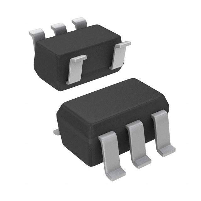
| 供应商器件封装 | SOT-23-5 |
| 其它名称 | 296-26126-1 |
| 包装 | 剪切带 (CT) |
| 单位重量 | 15.800 mg |
| 商标 | Texas Instruments |
| 回动电压—最大值 | 3 mV at 0 A |
| 安装类型 | 表面贴装 |
| 安装风格 | SMD/SMT |
| 封装 | Reel |
| 封装/外壳 | SC-74A,SOT-753 |
| 封装/箱体 | SOT-23-5 |
| 工作温度 | -40°C ~ 125°C |
| 工厂包装数量 | 250 |
| 最大工作温度 | + 125 C |
| 最大输入电压 | 16 V |
| 最小工作温度 | - 40 C |
| 最小输入电压 | + 2.2 V |
| 标准包装 | 1 |
| 电压-跌落(典型值) | 0.28V @ 150mA |
| 电压-输入 | 最高 16V |
| 电压-输出 | 5V |
| 电压调节准确度 | 1.5 % |
| 电流-输出 | 150mA |
| 电流-限制(最小值) | - |
| 稳压器拓扑 | 正,固定式 |
| 稳压器数 | 1 |
| 系列 | LP2985-50 |
| 线路调整率 | 0.014 % / V |
| 输入偏压电流—最大 | 0.85 mA |
| 输出电压 | 5 V |
| 输出电流 | 150 mA |
| 输出端数量 | 1 Output |
| 输出类型 | Fixed |


- 商务部:美国ITC正式对集成电路等产品启动337调查
- 曝三星4nm工艺存在良率问题 高通将骁龙8 Gen1或转产台积电
- 太阳诱电将投资9.5亿元在常州建新厂生产MLCC 预计2023年完工
- 英特尔发布欧洲新工厂建设计划 深化IDM 2.0 战略
- 台积电先进制程称霸业界 有大客户加持明年业绩稳了
- 达到5530亿美元!SIA预计今年全球半导体销售额将创下新高
- 英特尔拟将自动驾驶子公司Mobileye上市 估值或超500亿美元
- 三星加码芯片和SET,合并消费电子和移动部门,撤换高东真等 CEO
- 三星电子宣布重大人事变动 还合并消费电子和移动部门
- 海关总署:前11个月进口集成电路产品价值2.52万亿元 增长14.8%


PDF Datasheet 数据手册内容提取
Product Sample & Technical Tools & Support & Folder Buy Documents Software Community LP2985 SLVS522O–JULY2004–REVISEDJANUARY2015 LP2985 150-mA Low-noise Low-dropout Regulator With Shutdown 1 Features 3 Description • OutputToleranceof The LP2985 family of fixed-output, low-dropout 1 regulators offers exceptional, cost-effective – 1%(AGrade) performance for both portable and nonportable – 1.5%(StandardGrade) applications. Available in voltages of 1.8 V, 2.5 V, 2.8 • Ultra-LowDropout,Typically V, 2.9 V, 3 V, 3.1 V, 3.3 V, 5 V, and 10 V, the family hasanoutputtoleranceof1%fortheAversion(1.5% – 280mVatFullLoadof150mA for the non-A version) and is capable of delivering – 7mVat1mA 150-mA continuous load current. Standard regulator • WideV Range:16VMax features, such as overcurrent and overtemperature IN protection,areincluded. • LowI :850μAatFullLoadat150mA Q • ShutdownCurrent:0.01μATyp DeviceInformation(1) • LowNoise:30 μV With10-nFBypass RMS PARTNUMBER PACKAGE BODYSIZE(NOM) Capacitor LP2985 SOT-23(5) 2.90mmx1.60mm • StableWithLow-ESRCapacitors,Including (1) For all available packages, see the orderable addendum at Ceramic theendofthedatasheet. • OvercurrentandThermalProtection DropoutVoltagevsTemperature • HighPeak-CurrentCapability • ESDProtectionExceedsJESD22 0.45 VO= 3.3 V 150 mA – 2000-VHuman-BodyModel(A114-A) 0.4 Cbyp= 10 nF – 200-VMachineModel(A115-A) 0.35 2 Applications 0.3 V) • PortableDevices ( − 0.25 • DigitalCamerasandCamcorders ut o p • CDPlayers o 0.2 Dr • MP3Players 50 mA 0.15 0.1 10 mA 0.05 1 mA 0 −50 −25 0 25 50 75 100 125 150 Temperature−(°C) 1 An IMPORTANT NOTICE at the end of this data sheet addresses availability, warranty, changes, use in safety-critical applications, intellectualpropertymattersandotherimportantdisclaimers.PRODUCTIONDATA.
LP2985 SLVS522O–JULY2004–REVISEDJANUARY2015 www.ti.com Table of Contents 1 Features.................................................................. 1 7.2 FunctionalBlockDiagram.......................................11 2 Applications........................................................... 1 7.3 FeatureDescription.................................................11 3 Description............................................................. 1 7.4 DeviceFunctionalModes........................................11 4 RevisionHistory..................................................... 2 8 ApplicationandImplementation........................ 12 8.1 ApplicationInformation............................................12 5 PinConfigurationandFunctions......................... 3 9 PowerSupplyRecommendations...................... 16 6 Specifications......................................................... 4 10 Layout................................................................... 17 6.1 AbsoluteMaximumRatings.....................................4 6.2 ESDRatings..............................................................4 10.1 LayoutGuidelines.................................................17 6.3 RecommendedOperatingConditions......................4 10.2 LayoutExample....................................................17 6.4 ThermalInformation..................................................4 11 DeviceandDocumentationSupport................. 17 6.5 ElectricalCharacteristics..........................................5 11.1 Trademarks...........................................................17 6.6 TypicalCharacteristics..............................................7 11.2 ElectrostaticDischargeCaution............................17 7 DetailedDescription............................................ 11 11.3 Glossary................................................................17 7.1 Overview.................................................................11 12 Mechanical,Packaging,andOrderable Information........................................................... 17 4 Revision History ChangesfromRevisionN(June2011)toRevisionO Page • AddedApplications,DeviceInformationtable,PinFunctionstable,ESDRatingstable,ThermalInformationtable, FeatureDescriptionsection,DeviceFunctionalModes,ApplicationandImplementationsection,PowerSupply Recommendationssection,Layoutsection,DeviceandDocumentationSupportsection,andMechanical, Packaging,andOrderableInformationsection...................................................................................................................... 1 • DeletedOrderingInformationtable........................................................................................................................................ 1 2 SubmitDocumentationFeedback Copyright©2004–2015,TexasInstrumentsIncorporated
LP2985 www.ti.com SLVS522O–JULY2004–REVISEDJANUARY2015 5 Pin Configuration and Functions DBV (SOT-23) PACKAGE (TOPVIEW) V 1 5 V IN OUT GND 2 ON/OFF 3 4 BYPASS PinFunctions PIN TYPE DESCRIPTION NAME NO. BYPASS 4 I/O Attacha10-nFcapacitortoimprovelow-noiseperformance. GND 2 — Ground ON/OFF 3 I Active-lowshutdownpin.TietoV ifunused. IN V 1 I Supplyinput IN V 5 O Voltageoutput OUT Copyright©2004–2015,TexasInstrumentsIncorporated SubmitDocumentationFeedback 3
LP2985 SLVS522O–JULY2004–REVISEDJANUARY2015 www.ti.com 6 Specifications 6.1 Absolute Maximum Ratings overvirtualjunctiontemperaturerange(unlessotherwisenoted)(1) MIN MAX UNIT V Continuousinputvoltagerange(2) –0.3 16 V IN V ON/OFFinputvoltagerange –0.3 16 V ON/OFF Outputvoltagerange(3) –0.3 9 V I Outputcurrent(4) Internallylimited — O (short-circuitprotected) θ Packagethermalimpedance(4) (5) 206 °C/W JA T Operatingvirtualjunctiontemperature 150 °C J T Storagetemperaturerange –65 150 °C stg (1) Stressesbeyondthoselistedunder"absolutemaximumratings"maycausepermanentdamagetothedevice.Thesearestressratings only,andfunctionaloperationofthedeviceattheseoranyotherconditionsbeyondthoseindicatedunderRecommendedOperating Conditionsisnotimplied.Exposuretoabsolute-maximum-ratedconditionsforextendedperiodsmayaffectdevicereliability. (2) ThePNPpasstransistorhasaparasiticdiodeconnectedbetweentheinputandoutput.Thisdiodenormallyisreversebiased (V >V ),butwillbeforwardbiasediftheoutputvoltageexceedstheinputvoltagebyadiodedrop(seeApplicationInformationfor IN OUT moredetails). (3) Ifloadisreturnedtoanegativepowersupplyinadual-supplysystem,theoutputmustbediodeclampedtoGND. (4) MaximumpowerdissipationisafunctionofT(max),θ ,andT .Themaximumallowablepowerdissipationatanyallowableambient J JA A temperatureisP =(T(max)–T )/θ .OperatingattheabsolutemaximumT of150°Ccanaffectreliability. D J A JA J (5) ThepackagethermalimpedanceiscalculatedinaccordancewithJESD51-7. 6.2 ESD Ratings VALUE UNIT Humanbodymodel(HBM),perANSI/ESDA/JEDECJS-001,allpins(1) 2000 V(ESD) Electrostaticdischarge Chargeddevicemodel(CDM),perJEDECspecificationJESD22-C101, V allpins(2) 1000 (1) JEDECdocumentJEP155statesthat500-VHBMallowssafemanufacturingwithastandardESDcontrolprocess. (2) JEDECdocumentJEP157statesthat250-VCDMallowssafemanufacturingwithastandardESDcontrolprocess. 6.3 Recommended Operating Conditions MIN MAX UNIT V Supplyinputvoltage 2.2(1) 16 V IN V ON/OFFinputvoltage 0 V V ON/OFF IN I Outputcurrent 150 mA OUT T Virtualjunctiontemperature –40 125 °C J (1) RecommendedminimumV isthegreaterof2.5VorV +rateddropoutvoltage(max)foroperatingI . IN OUT(max) L 6.4 Thermal Information LP2985 THERMALMETRIC(1) DBV UNIT 5PINS R Junction-to-ambientthermalresistance 206 °C/W θJA (1) Formoreinformationabouttraditionalandnewthermalmetrics,seetheICPackageThermalMetricsapplicationreport,SPRA953. 4 SubmitDocumentationFeedback Copyright©2004–2015,TexasInstrumentsIncorporated
LP2985 www.ti.com SLVS522O–JULY2004–REVISEDJANUARY2015 6.5 Electrical Characteristics atspecifiedvirtualjunctiontemperaturerange,V =V +1V,V =2V,C =1μF,I =1mA,C =4.7μF IN OUT(NOM) ON/OFF IN L OUT (unlessotherwisenoted) LP2985A-xx LP2985-xx PARAMETER TESTCONDITIONS TJ UNIT MIN TYP MAX MIN TYP MAX IL=1mA 25°C –1 1 –1.5 1.5 25°C –1.5 1.5 –2.5 2.5 Outputvoltage 1mA≤IL≤50mA ΔVOUT tolerance –40°Cto125°C –2.5 2.5 –3.5 3.5 %VNOM 25°C –2.5 2.5 –3 3 1mA≤IL≤150mA –40°Cto125°C –3.5 3.5 –4 4 25°C 0.007 0.014 0.007 0.014 Lineregulation VIN=[VOUT(NOM)+1V]to16V %/V –40°Cto125°C 0.032 0.032 25°C 1 3 1 3 IL=0 –40°Cto125°C 5 5 25°C 7 10 7 10 IL=1mA –40°Cto125°C 15 15 25°C 40 60 40 60 VIN–VOUT Dropoutvoltage(1) IL=10mA mV –40°Cto125°C 90 90 25°C 120 150 120 150 IL=50mA –40°Cto125°C 225 225 25°C 280 350 280 350 IL=150mA –40°Cto125°C 575 575 25°C 65 95 65 95 25°C(LP2985-10) 125 125 IL=0 –40°Cto125°C 125 125 –40°Cto125°C 160 160 (LP2985-10) 25°C 75 110 75 110 IL=1mA 25°C(LP2985-10) 140 140 –40°Cto125°C 170 170 25°C 120 220 120 220 IL=10mA 25°C(LP2985-10) 250 250 IGND GNDpincurrent –40°Cto125°C 400 400 μA 25°C 350 600 350 600 IL=50mA 25°C(LP2985-10) 650 650 –40°Cto125°C 1000 1000 25°C 850 1500 850 1500 IL=150mA 25°C(LP2985-10) 1800 1800 –40°Cto125°C 2500 2500 VON/OFF<0.3V(OFF) 25°C 0.01 0.8 0.01 0.8 –40°Cto105°C 0.05 2 0.05 2 VON/OFF<0.15V(OFF) –40°Cto125°C 5 5 25°C 1.4 1.4 VON/OFF=HIGH→O/PON –40°Cto125°C 1.6 1.6 VON/OFF ON/OFFinputvoltage(2) V 25°C 0.55 0.55 VON/OFF=LOW→O/POFF –40°Cto125°C 0.15 0.15 25°C 0.01 0.01 VON/OFF=0 –40°Cto125°C –2 –2 ION/OFF ON/OFFinputcurrent μA 25°C 5 5 VON/OFF=5V –40°Cto125°C 15 15 (1) Dropoutvoltageisdefinedastheinput-to-outputdifferentialatwhichtheoutputvoltagedrops100mVbelowthevaluemeasuredwitha 1-Vdifferential. (2) TheON/OFFinputmustbedrivenproperlyforreliableoperation(seeApplicationInformation). Copyright©2004–2015,TexasInstrumentsIncorporated SubmitDocumentationFeedback 5
LP2985 SLVS522O–JULY2004–REVISEDJANUARY2015 www.ti.com Electrical Characteristics (continued) atspecifiedvirtualjunctiontemperaturerange,V =V +1V,V =2V,C =1μF,I =1mA,C =4.7μF IN OUT(NOM) ON/OFF IN L OUT (unlessotherwisenoted) LP2985A-xx LP2985-xx PARAMETER TESTCONDITIONS TJ UNIT MIN TYP MAX MIN TYP MAX BW=300Hzto50kHz, Vn Outputnoise(RMS) COUT=10μF, 25°C 30 30 μV CBYPASS=10nF ΔVOUT/ Ripplerejection f=1kHz,COUT=10μF, 25°C 45 45 dB ΔVIN CBYPASS=10nF IOUT(PK) Peakoutputcurrent VOUT≥VO(NOM)–5% 25°C 350 350 mA IOUT(SC) Short-circuitcurrent RL=0(steadystate)(3) 25°C 400 400 mA (3) SeeFigure6inTypicalPerformanceCharacteristics. 6 SubmitDocumentationFeedback Copyright©2004–2015,TexasInstrumentsIncorporated
LP2985 www.ti.com SLVS522O–JULY2004–REVISEDJANUARY2015 6.6 Typical Characteristics C =1μF,C =4.7μF,V =V +1V,T =25°C,ON/OFFpintiedtoV (unlessotherwisespecified) IN OUT IN OUT(NOM) A IN 10.20 3.345 VI=11V VI= 4.3 V 10.15 VCOI==110µFV 3.335 VCCOoi=== 1 43m..73F mVF –V 10.10 CIOO==14m.7AµF −(V) IO= 1 mA e e 3.325 utputVoltag 1100..0005 Output oltagV 3.315 O 9.95 3.305 9.90 9.85 3.295 −50 −25 0 25 50 75 100 125 150 -50 -25 0 25 50 75 100 125 150 Temperature−(°C) Temperature–°C Figure2.OutputVoltagevsTemperature Figure1.OutputVoltagevsTemperature 0.45 0.5 VO= 3.3 V 150 mA VI= 6 V 0.4 Cbyp= 10 nF 0.45 VO= 3.3 V Ci= 1mF 0.35 A) 0.4 Cbyp= 0.01mF ( − 0.35 Dropout−(V) 000.2..235 Circuit Current 000.2..235 0.15 50 mA hort- 0.15 S 0.1 0.1 0.05 10 mA 0.05 1 mA 0 0 −50 −25 0 25 50 75 100 125 150 −500 0 500 1000 1500 2000 Temperature−(°C) Time−(ms) Figure3.DropoutVoltagevsTemperature Figure4.Short-circuitCurrentvsTime 0.5 320 VI= 16 V 0.45 VO= 3.3 V VO= 3.3 V Ci= 1mF 300 A) 0.4 Cbyp= 0.01mF ( − Short-Circuit Current 00000...123..23555 I−(mA)SC 222468000 0.1 220 0.05 0 200 −100 100 300 500 700 0 0.5 1 1.5 2 2.5 3 3.5 Time−(ms) Output Voltage−(V) Figure5.Short-circuitCurrentvsTime Figure6.Short-circuitCurrentvsOutputVoltage Copyright©2004–2015,TexasInstrumentsIncorporated SubmitDocumentationFeedback 7
LP2985 SLVS522O–JULY2004–REVISEDJANUARY2015 www.ti.com Typical Characteristics (continued) C =1μF,C =4.7μF,V =V +1V,T =25°C,ON/OFFpintiedtoV (unlessotherwisespecified) IN OUT IN OUT(NOM) A IN 1200 100 1100 VCOby=p =3. 31 0V nF 90 VVIO== 53 V.3 V 1000 80 Co= 10mF 900 B) Cbyp= 0 nF A−m 800 −(d 70 1 mA 50 mA Current 670000 ejection 5600 ound Pin 450000 Ripple R 3400 150 mA Gr 300 20 200 10 100 0 0 0 20 40 60 80 100 120 140 160 10 100 1k 10k 100k 1M Load Current−mA Frequency−(Hz) Figure7.GroundPinCurrentvsLoadCurrent Figure8.RippleRejectionvsFrequency 100 100 VI= 3.7 V VI= 5 V 90 VO=3.3 V 90 VO=3.3 V B)80 CCoby=p 1=0 0m nFF B) 80 CCoby=p 4=. 710m FnF (d70 (d 70 − 1 mA − on60 on 60 1 mA cti cti eje50 50 mA eje 50 R R ple 40 ple 40 50 mA p p Ri30 Ri 30 150 mA 20 20 150 mA 10 10 0 0 10 100 1k 10k 100k 1M 10 100 1k 10k 100k 1M Frequency−(Hz) Frequency−(Hz) Figure9.RippleRejectionvsFrequency Figure10.RippleRejectionvsFrequency 100 10 8900 VVCIOo=== 5 43 V..73 mVF CCVOio=== 1 130m.3Fm VF Rejection−(dB) 567000 Cbyp1= m10A 1n0F mA (mped)ance−W 0.11 1 mA10 mA100 mA Ripple 3400 100 mA Output I 0.01 20 10 0 0.001 10 100 1k 10k 100k 1M 10 100 1k 10k 100k 1M Frequency−(Hz) Frequency−(Hz) Figure11.RippleRejectionvsFrequency Figure12.OutputImpedancevsFrequency 8 SubmitDocumentationFeedback Copyright©2004–2015,TexasInstrumentsIncorporated
LP2985 www.ti.com SLVS522O–JULY2004–REVISEDJANUARY2015 Typical Characteristics (continued) C =1μF,C =4.7μF,V =V +1V,T =25°C,ON/OFFpintiedtoV (unlessotherwisespecified) IN OUT IN OUT(NOM) A IN 10 10 CCio== 14.m7FmF ILOAD= 150 mA VO= 3.3 V 1 1 mA z) )W H (pedance− 0.1 10 mA100 mA (V/nsity−m 1 CbCypby=p 1= n1F00 pF Output Im 0.01 Noise De 0.1 Cbyp= 10 nF 0.001 0.01 10 100 1k 10k 100k 1M 100 1k 10k 100k Frequency−(Hz) Frequency−(Hz) Figure13.OutputImpedancevsFrequency Figure14.OutputNoiseDensityvsFrequency 10 1.8 ILOAD= 1 mA VO= 3.3 V 1.6 Cbyp= 10 nF RL= 3.3 kW z) 1.4 H A) (V/m 1 Cbyp= 100 pF −(m 1.2 nsity− Cbyp= 1 nF urrent 1 Noise De 0.1 Cbyp= 10 nF Input C 00..68 RL= Open 0.4 0.2 0.01 0 100 1k 10k 100k 0 1 2 3 4 5 6 Frequency−(Hz) Input Voltage−(V) Figure15.OutputNoiseDensityvsFrequency Figure16.InputCurrentvsInputVoltage 1400 VO= 3.3 V 1200 Cbyp= 10 nF 150 mA C) 1000 ( − ent 800 urr C d 600 n u Gro 400 1 mA 50 mA 0 mA 200 10 mA 0 −50 −25 0 25 50 75 100 125 150 Figure18.2.2-μFStableESRRange Temperature−(°C) forOutputVoltage≤2.3V Figure17.Ground-pinCurrentvsTemperature Copyright©2004–2015,TexasInstrumentsIncorporated SubmitDocumentationFeedback 9
LP2985 SLVS522O–JULY2004–REVISEDJANUARY2015 www.ti.com Typical Characteristics (continued) C =1μF,C =4.7μF,V =V +1V,T =25°C,ON/OFFpintiedtoV (unlessotherwisespecified) IN OUT IN OUT(NOM) A IN Figure20.2.2-μF/3.3-μFStableESRRange Figure19.4.7-μFStableESRRange forOutputVoltage≥2.5V forOutputVoltage≤2.3V 10 SubmitDocumentationFeedback Copyright©2004–2015,TexasInstrumentsIncorporated
LP2985 www.ti.com SLVS522O–JULY2004–REVISEDJANUARY2015 7 Detailed Description 7.1 Overview The LP2985 family of fixed-output, low-dropout regulators offers exceptional, cost-effective performance for both portable and nonportable applications. Available in voltages of 1.8 V, 2.5 V, 2.8 V, 2.9 V, 3 V, 3.1 V, 3.3 V, 5 V, and 10 V, the family has an output tolerance of 1% for the A version (1.5% for the non-A version) and is capable of delivering 150-mA continuous load current. Standard regulator features, such as overcurrent and overtemperatureprotection,areincluded. 7.2 Functional Block Diagram VIN ON/OFF 1.23 V VREF − + BYPASS VOUT Overcurrent/ Overtemperature Protection 7.3 Feature Description The LP2985 has a host of features that makes the regulator an ideal candidate for a variety of portable applications: • Low dropout: A PNP pass element allows a typical dropout of 280 mV at 150-mA load current and 7 mV at 1- mAload. • Low quiescent current: The use of a vertical PNP process allows for quiescent currents that are considerably lowerthanthoseassociatedwithtraditionallateralPNPregulators. • Shutdown: A shutdown feature is available, allowing the regulator to consume only 0.01 μA when the ON/OFF pinispulledlow. • Low-ESR-capacitor friendly: The regulator is stable with low-ESR capacitors, allowing the use of small, inexpensive,ceramiccapacitorsincost-sensitiveapplications. • Low noise: A BYPASS pin allows for low-noise operation, with a typical output noise of 30 μV , with the RMS useofa10-nFbypasscapacitor. • Smallpackaging:Forthemostspace-constrainedneeds,theregulatorisavailableintheSOT-23package. 7.4 Device Functional Modes 7.4.1 NormalOperation In normal operation, the device will output a fixed voltage corresponding with the orderable part number. The devicecandeliver150mAofcontinuousloadcurrent. 7.4.2 ShutdownMode Set the ON/OFF pin low to shut down the device when V is still present. If a shutdown mode is not needed, tie IN the pin to V . For proper operation, do not leave ON/OFF unconnected, and apply a signal with a slew rate of IN ≥40mV/μs. Copyright©2004–2015,TexasInstrumentsIncorporated SubmitDocumentationFeedback 11
LP2985 SLVS522O–JULY2004–REVISEDJANUARY2015 www.ti.com 8 Application and Implementation NOTE Information in the following applications sections is not part of the TI component specification, and TI does not warrant its accuracy or completeness. TI’s customers are responsible for determining suitability of components for their purposes. Customers should validateandtesttheirdesignimplementationtoconfirmsystemfunctionality. 8.1 Application Information ThefollowingapplicationschematicshowsthestandardusageoftheLP2985asalow-dropoutregulator. 8.1.1 TypicalApplication LP2985 VIN 1 5 VOUT 2.2µF 1µF GND 2 ON/OFF 3 4 BYPASS 10 nF 8.1.2 DesignRequirements MinimumC valueforstability(canbeincreasedwithoutlimitforimprovedstabilityandtransientresponse) OUT ON/OFF mustbeactivelyterminated.ConnecttoV ifshutdownfeatureisnotused. IN OptionalBYPASScapacitorforlow-noiseoperation 8.1.3 Capacitors 8.1.3.1 InputCapacitor(C ) IN A minimum value of 1 μF (over the entire operating temperature range) is required at the input of the LP2985. In addition, this input capacitor should be located within 1 cm of the input pin and connected to a clean analog ground. There are no equivalent series resistance (ESR) requirements for this capacitor, and the capacitance canbeincreasedwithoutlimit. 12 SubmitDocumentationFeedback Copyright©2004–2015,TexasInstrumentsIncorporated
LP2985 www.ti.com SLVS522O–JULY2004–REVISEDJANUARY2015 Application Information (continued) 8.1.3.2 OutputCapacitor(C ) OUT As an advantage over other regulators, the LP2985 permits the use of low-ESR capacitors at the output, including ceramic capacitors that can have an ESR as low as 5 mΩ. Tantalum and film capacitors also can be used if size and cost are not issues. The output capacitor also should be located within 1 cm of the output pin andbereturnedtoacleananalogground. As with other PNP LDOs, stability conditions require the output capacitor to have a minimum capacitance and an ESRthatfallswithinacertainrange. • MinimumC :2.2μF(canbeincreasedwithoutlimittoimprovetransientresponsestabilitymargin) OUT • ESRrange:seeFigure18throughFigure20 It is critical that both the minimum capacitance and ESR requirement be met over the entire operating temperature range. Depending on the type of capacitors used, both these parameters can vary significantly with temperature(seecapacitorcharacteristics). 8.1.3.3 NoiseBypassCapacitor(C ) BYPASS TheLP2985allowsforlow-noiseperformancewiththeuseofabypasscapacitorthatisconnectedtotheinternal bandgap reference via the BYPASS pin. This high-impedance bandgap circuitry is biased in the microampere range and, thus, cannot be loaded significantly, otherwise, its output – and, correspondingly, the output of the regulator – changes. Thus, for best output accuracy, dc leakage current through C should be minimized as BYPASS muchaspossibleandnevershouldexceed100nA. A10-nFcapacitorisrecommendedforC .Ceramicandfilmcapacitorsarewellsuitedforthispurpose. BYPASS 8.1.3.4 ReverseInput-OutputVoltage ThereisaninherentdiodepresentacrossthePNPpasselementoftheLP2985. V V IN OUT With the anode connected to the output, this diode is reverse biased during normal operation, since the input voltage is higher than the output. However, if the output is pulled higher than the input for any reason, this diode is forward biased and can cause a parasitic silicon-controlled rectifier (SCR) to latch, resulting in high current flowing from the output to the input. Thus, to prevent possible damage to the regulator in any application where the output may be pulled above the input, or the input may be shorted to ground, an external Schottky diode should be connected between the output and input. With the anode on output, this Schottky limits the reverse voltageacrosstheoutputandinputpinsto ∼0.3V,preventingtheregulator’sinternaldiodefromforwardbiasing. Schottky VIN VOUT LP2985 Copyright©2004–2015,TexasInstrumentsIncorporated SubmitDocumentationFeedback 13
LP2985 SLVS522O–JULY2004–REVISEDJANUARY2015 www.ti.com Application Information (continued) 8.1.4 DetailedDesignProcedure 8.1.4.1 CapacitorCharacteristics 8.1.4.1.1 Ceramics Ceramic capacitors are ideal choices for use on the output of the LP2985 for several reasons. For capacitances in the range of 2.2 μF to 4.7 μF, ceramic capacitors have the lowest cost and the lowest ESR, making them choice candidates for filtering high-frequency noise. For instance, a typical 2.2-μF ceramic capacitor has an ESR intherangeof10mΩ to20mΩand,thus,satisfiesminimumESRrequirementsoftheregulator. Ceramic capacitors have one major disadvantage that must be taken into account – a poor temperature coefficient, where the capacitance can vary significantly with temperature. For instance, a large-value ceramic capacitor(≥2.2 μF)canlosemorethanhalfofitscapacitanceasthetemperaturerisesfrom25°Cto85°C.Thus, a 2.2-μF capacitor at 25°C drops well below the minimum C required for stability, as ambient temperature OUT rises. For this reason, select an output capacitor that maintains the minimum 2.2 μF required for stability over the entire operating temperature range. Note that there are some ceramic capacitors that can maintain a ±15% capacitancetoleranceovertemperature. 8.1.4.1.2 Tantalum Tantalum capacitors can be used at the output of the LP2985, but there are significant disadvantages that could prohibittheiruse: • In the 1-μF to 4.7-μF range, tantalum capacitors are more expensive than ceramics of the equivalent capacitanceandvoltageratings. • Tantalum capacitors have higher ESRs than their equivalent-sized ceramic counterparts. Thus, to meet the ESR requirements, a higher-capacitance tantalum may be required, at the expense of larger size and higher cost. • The ESR of a tantalum capacitor increases as temperature drops, as much as double from 25°C to –40°C. Thus,ESRmarginsmustbemaintainedoverthetemperaturerangetopreventregulatorinstability. 8.1.4.2 ON/OFF Operation The LP2985 allows for a shutdown mode via the ON/OFF pin. Driving the pin LOW (≤ 0.3 V) turns the device OFF; conversely, a HIGH (≥ 1.6 V) turns the device ON. If the shutdown feature is not used, ON/OFF should be connected to the input to ensure that the regulator is on at all times. For proper operation, do not leave ON/OFF unconnected,andapplyasignalwithaslewrateof ≥ 40mV/μs. 8.1.5 ApplicationCurves 3.4 200 3.4 200 3.38 150 3.38 150 3.36 100 3.36 100 Output Voltage−(V) 3333...233.3824 VCDIObLy==p =31. 0310 0V mnFA IVLO −−05015000Load Current−(mA) Output Voltage−(V) 3333...233.3824 VCDIObLy==p =31. 5310 0V mnFA IVLO −−05015000Load Current−(mA) 3.26 −150 3.26 −150 3.24 −200 3.24 −200 3.22 −250 3.22 −250 20ms/div→ 20ms/div→ Figure21.LoadTransientResponse Figure22.LoadTransientResponse 14 SubmitDocumentationFeedback Copyright©2004–2015,TexasInstrumentsIncorporated
LP2985 www.ti.com SLVS522O–JULY2004–REVISEDJANUARY2015 Application Information (continued) 3.4 200 3.41 5.5 3.38 150 3.39 5 3.36 100 3.37 VI 4.5 Output oltage−V(V) 3333...233.3824 VCDIObLy==p =31. 5300 V nmFA VILO −−50015000 Load Current−(mA) Ooutput Vltage−(V)333...333135 VCIOOb=y=p 1 =35. 030 mVnFA VO 334.5 Input oltageV−(V) 3.26 −150 3.29 2.5 3.24 −200 3.22 −250 3.27 2 20ms/div→ 20ms/div→ Figure23.LoadTransientResponse Figure24.LineTransientResponse 3.41 5.5 3.41 5.5 3.39 5 3.39 5 Outpoltagut Ve−(V)333...333357 VCIOOb=y=p 1 =35. 031 0mV nAF VI 344..55 Input Voltage−(V) Output oltageV−(V)333...333357 VCIOOb=y=p 1 =3 m. 30A VnF VI 344..55 Input Voltage−(V) 3.31 3 3.31 3 3.29 VO 2.5 3.29 2.5 VO 3.27 2 3.27 2 20ms/div→ 20ms/div→ Figure25.LineTransientResponse Figure26.LineTransientResponse 3.41 5.5 4 10 VO 3.39 5 3 8 3.37 VIN 4.5 2 Output Voltage−(V)33..3335 VCIOOb=y=p 1 =3 m. 31A 0V nF 34.5 Inpuoltat Vge−(V) Output Voltage−(V)−011 VCOby=p =3. 30 V 46V−(V)ON/OFF 3.31 3 IO= 150 mA VO −2 VON/OFF 2 3.29 2.5 −3 3.27 2 −4 0 100ms/div→ 100ms/div→ Figure27.LineTransientResponse Figure28.Turn-onTime Copyright©2004–2015,TexasInstrumentsIncorporated SubmitDocumentationFeedback 15
LP2985 SLVS522O–JULY2004–REVISEDJANUARY2015 www.ti.com Application Information (continued) 4 10 4 10 VO VO 3 3 8 8 2 2 V) (V) ge−( 1 6 −(V) age− 1 6 −(V) Output Volta−01 VCOby=p =3. 31 0V0 pF 4 VON/OFF Outoltput V−01 VCOby=p =3. 31 VnF 4 VON/OFF ILOAD= 150 mA ILOAD= 150 mA −2 VON/OFF −2 VON/OFF 2 2 −3 −3 −4 0 −4 0 2 ms/div→ 200ms/div→ Figure30.Turn-onTime Figure29.Turn-onTime 4 10 Input 3 8 2 V) ( ge− 1 6 (V) a − Volt 0 OFF Output −1 VCOby=p =3. 31 0V nF 4 VON/ ILOAD= 150 mA −2 Output 2 −3 −4 0 20 ms/div→ Figure31.Turn-onTime 9 Power Supply Recommendations A power supply may be used at the input voltage within the ranges given in the Recommended Operating Conditionstable.ItisrecommendedtousebypasscapacitorsasdescribedinLayoutGuidelines. 16 SubmitDocumentationFeedback Copyright©2004–2015,TexasInstrumentsIncorporated
LP2985 www.ti.com SLVS522O–JULY2004–REVISEDJANUARY2015 10 Layout 10.1 Layout Guidelines • Itisrecommendedthattheinputpinbebypassedtogroundwithabypass-capacitor. • The optimum placement of the bypass capacitor is closest to the V of the device and GND of the system. IN Care must be taken to minimize the loop area formed by the bypass-capacitor connection, the V pin, and IN theGNDpinofthesystem. • For operation at full-rated load, it is recommended to use wide trace lengths to eliminate IR drop and heat dissipation. 10.2 Layout Example V V IN OUT 1 5 1 (cid:29)F 2.2 (cid:29)F 2 LP2985 3 4 ON/OFF 10 nF tied to V IN if not used Figure32. LayoutDiagram 11 Device and Documentation Support 11.1 Trademarks Alltrademarksarethepropertyoftheirrespectiveowners. 11.2 Electrostatic Discharge Caution Thesedeviceshavelimitedbuilt-inESDprotection.Theleadsshouldbeshortedtogetherorthedeviceplacedinconductivefoam duringstorageorhandlingtopreventelectrostaticdamagetotheMOSgates. 11.3 Glossary SLYZ022—TIGlossary. Thisglossarylistsandexplainsterms,acronyms,anddefinitions. 12 Mechanical, Packaging, and Orderable Information The following pages include mechanical, packaging, and orderable information. This information is the most current data available for the designated devices. This data is subject to change without notice and revision of thisdocument.Forbrowser-basedversionsofthisdatasheet,refertotheleft-handnavigation. Copyright©2004–2015,TexasInstrumentsIncorporated SubmitDocumentationFeedback 17
PACKAGE OPTION ADDENDUM www.ti.com 24-Aug-2018 PACKAGING INFORMATION Orderable Device Status Package Type Package Pins Package Eco Plan Lead/Ball Finish MSL Peak Temp Op Temp (°C) Device Marking Samples (1) Drawing Qty (2) (6) (3) (4/5) LP2985-10DBVR ACTIVE SOT-23 DBV 5 3000 Green (RoHS CU NIPDAU Level-1-260C-UNLIM -40 to 125 LRCG & no Sb/Br) LP2985-10DBVT ACTIVE SOT-23 DBV 5 250 Green (RoHS CU NIPDAU Level-1-260C-UNLIM -40 to 125 LRCG & no Sb/Br) LP2985-18DBVR ACTIVE SOT-23 DBV 5 3000 Green (RoHS CU NIPDAU | CU SN Level-1-260C-UNLIM -40 to 125 (LPHG, LPHL) & no Sb/Br) LP2985-18DBVRE4 ACTIVE SOT-23 DBV 5 3000 Green (RoHS CU NIPDAU Level-1-260C-UNLIM -40 to 125 LPHG & no Sb/Br) LP2985-18DBVRG4 ACTIVE SOT-23 DBV 5 3000 Green (RoHS CU NIPDAU Level-1-260C-UNLIM -40 to 125 LPHG & no Sb/Br) LP2985-18DBVT ACTIVE SOT-23 DBV 5 250 Green (RoHS CU NIPDAU | CU SN Level-1-260C-UNLIM -40 to 125 (LPHG, LPHL) & no Sb/Br) LP2985-18DBVTE4 ACTIVE SOT-23 DBV 5 250 Green (RoHS CU NIPDAU Level-1-260C-UNLIM -40 to 125 LPHG & no Sb/Br) LP2985-18DBVTG4 ACTIVE SOT-23 DBV 5 250 Green (RoHS CU NIPDAU Level-1-260C-UNLIM -40 to 125 LPHG & no Sb/Br) LP2985-25DBVR ACTIVE SOT-23 DBV 5 3000 Green (RoHS CU NIPDAU Level-1-260C-UNLIM -40 to 125 (LPLG, LPLL) & no Sb/Br) LP2985-25DBVT ACTIVE SOT-23 DBV 5 250 Green (RoHS CU NIPDAU Level-1-260C-UNLIM -40 to 125 (LPLG, LPLL) & no Sb/Br) LP2985-28DBVR ACTIVE SOT-23 DBV 5 3000 Green (RoHS CU NIPDAU | CU SN Level-1-260C-UNLIM -40 to 125 (LPGG, LPGL) & no Sb/Br) LP2985-28DBVT ACTIVE SOT-23 DBV 5 250 Green (RoHS CU NIPDAU | CU SN Level-1-260C-UNLIM -40 to 125 (LPGG, LPGL) & no Sb/Br) LP2985-28DBVTG4 ACTIVE SOT-23 DBV 5 250 Green (RoHS CU NIPDAU Level-1-260C-UNLIM -40 to 125 LPGG & no Sb/Br) LP2985-29DBVR ACTIVE SOT-23 DBV 5 3000 Green (RoHS CU NIPDAU Level-1-260C-UNLIM -40 to 125 (LPMG, LPML) & no Sb/Br) LP2985-30DBVR ACTIVE SOT-23 DBV 5 3000 Green (RoHS CU NIPDAU Level-1-260C-UNLIM -40 to 125 (LPNG, LPNL) & no Sb/Br) LP2985-30DBVRG4 ACTIVE SOT-23 DBV 5 3000 Green (RoHS CU NIPDAU Level-1-260C-UNLIM -40 to 125 (LPNG, LPNL) & no Sb/Br) LP2985-30DBVT ACTIVE SOT-23 DBV 5 250 Green (RoHS CU NIPDAU Level-1-260C-UNLIM -40 to 125 (LPNG, LPNL) & no Sb/Br) Addendum-Page 1
PACKAGE OPTION ADDENDUM www.ti.com 24-Aug-2018 Orderable Device Status Package Type Package Pins Package Eco Plan Lead/Ball Finish MSL Peak Temp Op Temp (°C) Device Marking Samples (1) Drawing Qty (2) (6) (3) (4/5) LP2985-30DBVTG4 ACTIVE SOT-23 DBV 5 250 Green (RoHS CU NIPDAU Level-1-260C-UNLIM -40 to 125 (LPNG, LPNL) & no Sb/Br) LP2985-33DBVR ACTIVE SOT-23 DBV 5 3000 Green (RoHS CU NIPDAU | CU SN Level-1-260C-UNLIM -40 to 125 (LPFG, LPFL) & no Sb/Br) LP2985-33DBVRE4 ACTIVE SOT-23 DBV 5 3000 Green (RoHS CU NIPDAU Level-1-260C-UNLIM -40 to 125 LPFG & no Sb/Br) LP2985-33DBVRG4 ACTIVE SOT-23 DBV 5 3000 Green (RoHS CU NIPDAU Level-1-260C-UNLIM -40 to 125 LPFG & no Sb/Br) LP2985-33DBVT ACTIVE SOT-23 DBV 5 250 Green (RoHS CU NIPDAU | CU SN Level-1-260C-UNLIM -40 to 125 (LPFG, LPFL) & no Sb/Br) LP2985-33DBVTE4 ACTIVE SOT-23 DBV 5 250 Green (RoHS CU NIPDAU Level-1-260C-UNLIM -40 to 125 LPFG & no Sb/Br) LP2985-33DBVTG4 ACTIVE SOT-23 DBV 5 250 Green (RoHS CU NIPDAU Level-1-260C-UNLIM -40 to 125 LPFG & no Sb/Br) LP2985-50DBVR ACTIVE SOT-23 DBV 5 3000 Green (RoHS CU NIPDAU Level-1-260C-UNLIM -40 to 125 (LPSG, LPSL) & no Sb/Br) LP2985-50DBVRG4 ACTIVE SOT-23 DBV 5 3000 Green (RoHS CU NIPDAU Level-1-260C-UNLIM -40 to 125 (LPSG, LPSL) & no Sb/Br) LP2985-50DBVT ACTIVE SOT-23 DBV 5 250 Green (RoHS CU NIPDAU Level-1-260C-UNLIM -40 to 125 (LPSG, LPSL) & no Sb/Br) LP2985-50DBVTG4 ACTIVE SOT-23 DBV 5 250 Green (RoHS CU NIPDAU Level-1-260C-UNLIM -40 to 125 (LPSG, LPSL) & no Sb/Br) LP2985A-10DBVR ACTIVE SOT-23 DBV 5 3000 Green (RoHS CU NIPDAU Level-1-260C-UNLIM -40 to 125 LRDG & no Sb/Br) LP2985A-10DBVT ACTIVE SOT-23 DBV 5 250 Green (RoHS CU NIPDAU Level-1-260C-UNLIM -40 to 125 LRDG & no Sb/Br) LP2985A-18DBVJ ACTIVE SOT-23 DBV 5 10000 Green (RoHS CU NIPDAU Level-1-260C-UNLIM -40 to 125 LPTL & no Sb/Br) LP2985A-18DBVR ACTIVE SOT-23 DBV 5 3000 Green (RoHS CU NIPDAU | CU SN Level-1-260C-UNLIM -40 to 125 (LPTG, LPTL) & no Sb/Br) LP2985A-18DBVRG4 ACTIVE SOT-23 DBV 5 3000 Green (RoHS CU NIPDAU Level-1-260C-UNLIM -40 to 125 LPTG & no Sb/Br) LP2985A-18DBVT ACTIVE SOT-23 DBV 5 250 Green (RoHS CU NIPDAU | CU SN Level-1-260C-UNLIM -40 to 125 (LPTG, LPTL) & no Sb/Br) LP2985A-25DBVR ACTIVE SOT-23 DBV 5 3000 Green (RoHS CU NIPDAU Level-1-260C-UNLIM -40 to 125 (LPUG, LPUL) & no Sb/Br) Addendum-Page 2
PACKAGE OPTION ADDENDUM www.ti.com 24-Aug-2018 Orderable Device Status Package Type Package Pins Package Eco Plan Lead/Ball Finish MSL Peak Temp Op Temp (°C) Device Marking Samples (1) Drawing Qty (2) (6) (3) (4/5) LP2985A-25DBVRG4 ACTIVE SOT-23 DBV 5 3000 Green (RoHS CU NIPDAU Level-1-260C-UNLIM -40 to 125 (LPUG, LPUL) & no Sb/Br) LP2985A-25DBVT ACTIVE SOT-23 DBV 5 250 Green (RoHS CU NIPDAU Level-1-260C-UNLIM -40 to 125 (LPUG, LPUL) & no Sb/Br) LP2985A-28DBVR ACTIVE SOT-23 DBV 5 3000 Green (RoHS CU NIPDAU | CU SN Level-1-260C-UNLIM -40 to 125 (LPJG, LPJL) & no Sb/Br) LP2985A-28DBVT ACTIVE SOT-23 DBV 5 250 Green (RoHS CU NIPDAU | CU SN Level-1-260C-UNLIM -40 to 125 (LPJG, LPJL) & no Sb/Br) LP2985A-29DBVR ACTIVE SOT-23 DBV 5 3000 Green (RoHS CU NIPDAU Level-1-260C-UNLIM -40 to 125 (LPZG, LPZL) & no Sb/Br) LP2985A-30DBVR ACTIVE SOT-23 DBV 5 3000 Green (RoHS CU NIPDAU Level-1-260C-UNLIM -40 to 125 (LRAG, LRAL) & no Sb/Br) LP2985A-30DBVT ACTIVE SOT-23 DBV 5 250 Green (RoHS CU NIPDAU Level-1-260C-UNLIM -40 to 125 (LRAG, LRAL) & no Sb/Br) LP2985A-33DBVR ACTIVE SOT-23 DBV 5 3000 Green (RoHS CU NIPDAU | CU SN Level-1-260C-UNLIM -40 to 125 (LPKG, LPKL) & no Sb/Br) LP2985A-33DBVRG4 ACTIVE SOT-23 DBV 5 3000 Green (RoHS CU NIPDAU Level-1-260C-UNLIM -40 to 125 LPKG & no Sb/Br) LP2985A-33DBVT ACTIVE SOT-23 DBV 5 250 Green (RoHS CU NIPDAU | CU SN Level-1-260C-UNLIM -40 to 125 (LPKG, LPKL) & no Sb/Br) LP2985A-33DBVTE4 ACTIVE SOT-23 DBV 5 250 Green (RoHS CU NIPDAU Level-1-260C-UNLIM -40 to 125 LPKG & no Sb/Br) LP2985A-33DBVTG4 ACTIVE SOT-23 DBV 5 250 Green (RoHS CU NIPDAU Level-1-260C-UNLIM -40 to 125 LPKG & no Sb/Br) LP2985A-50DBVR ACTIVE SOT-23 DBV 5 3000 Green (RoHS CU NIPDAU Level-1-260C-UNLIM -40 to 125 (LR1G, LR1L) & no Sb/Br) LP2985A-50DBVRG4 ACTIVE SOT-23 DBV 5 3000 Green (RoHS CU NIPDAU Level-1-260C-UNLIM -40 to 125 (LR1G, LR1L) & no Sb/Br) LP2985A-50DBVT ACTIVE SOT-23 DBV 5 250 Green (RoHS CU NIPDAU Level-1-260C-UNLIM -40 to 125 (LR1G, LR1L) & no Sb/Br) (1) The marketing status values are defined as follows: ACTIVE: Product device recommended for new designs. LIFEBUY: TI has announced that the device will be discontinued, and a lifetime-buy period is in effect. NRND: Not recommended for new designs. Device is in production to support existing customers, but TI does not recommend using this part in a new design. PREVIEW: Device has been announced but is not in production. Samples may or may not be available. OBSOLETE: TI has discontinued the production of the device. Addendum-Page 3
PACKAGE OPTION ADDENDUM www.ti.com 24-Aug-2018 (2) RoHS: TI defines "RoHS" to mean semiconductor products that are compliant with the current EU RoHS requirements for all 10 RoHS substances, including the requirement that RoHS substance do not exceed 0.1% by weight in homogeneous materials. Where designed to be soldered at high temperatures, "RoHS" products are suitable for use in specified lead-free processes. TI may reference these types of products as "Pb-Free". RoHS Exempt: TI defines "RoHS Exempt" to mean products that contain lead but are compliant with EU RoHS pursuant to a specific EU RoHS exemption. Green: TI defines "Green" to mean the content of Chlorine (Cl) and Bromine (Br) based flame retardants meet JS709B low halogen requirements of <=1000ppm threshold. Antimony trioxide based flame retardants must also meet the <=1000ppm threshold requirement. (3) MSL, Peak Temp. - The Moisture Sensitivity Level rating according to the JEDEC industry standard classifications, and peak solder temperature. (4) There may be additional marking, which relates to the logo, the lot trace code information, or the environmental category on the device. (5) Multiple Device Markings will be inside parentheses. Only one Device Marking contained in parentheses and separated by a "~" will appear on a device. If a line is indented then it is a continuation of the previous line and the two combined represent the entire Device Marking for that device. (6) Lead/Ball Finish - Orderable Devices may have multiple material finish options. Finish options are separated by a vertical ruled line. Lead/Ball Finish values may wrap to two lines if the finish value exceeds the maximum column width. Important Information and Disclaimer:The information provided on this page represents TI's knowledge and belief as of the date that it is provided. TI bases its knowledge and belief on information provided by third parties, and makes no representation or warranty as to the accuracy of such information. Efforts are underway to better integrate information from third parties. TI has taken and continues to take reasonable steps to provide representative and accurate information but may not have conducted destructive testing or chemical analysis on incoming materials and chemicals. TI and TI suppliers consider certain information to be proprietary, and thus CAS numbers and other limited information may not be available for release. In no event shall TI's liability arising out of such information exceed the total purchase price of the TI part(s) at issue in this document sold by TI to Customer on an annual basis. Addendum-Page 4
PACKAGE MATERIALS INFORMATION www.ti.com 1-Feb-2018 TAPE AND REEL INFORMATION *Alldimensionsarenominal Device Package Package Pins SPQ Reel Reel A0 B0 K0 P1 W Pin1 Type Drawing Diameter Width (mm) (mm) (mm) (mm) (mm) Quadrant (mm) W1(mm) LP2985-10DBVR SOT-23 DBV 5 3000 178.0 9.0 3.23 3.17 1.37 4.0 8.0 Q3 LP2985-10DBVT SOT-23 DBV 5 250 178.0 9.0 3.3 3.2 1.4 4.0 8.0 Q3 LP2985-18DBVR SOT-23 DBV 5 3000 178.0 9.0 3.3 3.2 1.4 4.0 8.0 Q3 LP2985-18DBVRG4 SOT-23 DBV 5 3000 178.0 9.0 3.3 3.2 1.4 4.0 8.0 Q3 LP2985-18DBVTG4 SOT-23 DBV 5 250 178.0 9.0 3.23 3.17 1.37 4.0 8.0 Q3 LP2985-25DBVR SOT-23 DBV 5 3000 178.0 9.0 3.3 3.2 1.4 4.0 8.0 Q3 LP2985-28DBVR SOT-23 DBV 5 3000 178.0 9.0 3.23 3.17 1.37 4.0 8.0 Q3 LP2985-28DBVTG4 SOT-23 DBV 5 250 178.0 9.0 3.3 3.2 1.4 4.0 8.0 Q3 LP2985-29DBVR SOT-23 DBV 5 3000 178.0 9.0 3.23 3.17 1.37 4.0 8.0 Q3 LP2985-30DBVR SOT-23 DBV 5 3000 178.0 9.0 3.23 3.17 1.37 4.0 8.0 Q3 LP2985-33DBVR SOT-23 DBV 5 3000 178.0 9.0 3.3 3.2 1.4 4.0 8.0 Q3 LP2985-33DBVRG4 SOT-23 DBV 5 3000 178.0 9.0 3.3 3.2 1.4 4.0 8.0 Q3 LP2985-33DBVT SOT-23 DBV 5 250 178.0 9.0 3.23 3.17 1.37 4.0 8.0 Q3 LP2985-33DBVTG4 SOT-23 DBV 5 250 178.0 9.0 3.23 3.17 1.37 4.0 8.0 Q3 LP2985-50DBVR SOT-23 DBV 5 3000 178.0 9.0 3.23 3.17 1.37 4.0 8.0 Q3 LP2985A-10DBVR SOT-23 DBV 5 3000 178.0 9.0 3.23 3.17 1.37 4.0 8.0 Q3 LP2985A-10DBVT SOT-23 DBV 5 250 178.0 9.0 3.3 3.2 1.4 4.0 8.0 Q3 LP2985A-18DBVJ SOT-23 DBV 5 10000 330.0 8.4 3.17 3.23 1.37 4.0 8.0 Q3 PackMaterials-Page1
PACKAGE MATERIALS INFORMATION www.ti.com 1-Feb-2018 Device Package Package Pins SPQ Reel Reel A0 B0 K0 P1 W Pin1 Type Drawing Diameter Width (mm) (mm) (mm) (mm) (mm) Quadrant (mm) W1(mm) LP2985A-18DBVR SOT-23 DBV 5 3000 178.0 9.0 3.23 3.17 1.37 4.0 8.0 Q3 LP2985A-18DBVRG4 SOT-23 DBV 5 3000 178.0 9.0 3.23 3.17 1.37 4.0 8.0 Q3 LP2985A-25DBVR SOT-23 DBV 5 3000 178.0 9.0 3.23 3.17 1.37 4.0 8.0 Q3 LP2985A-25DBVT SOT-23 DBV 5 250 180.0 9.2 3.17 3.23 1.37 4.0 8.0 Q3 LP2985A-28DBVR SOT-23 DBV 5 3000 178.0 9.0 3.23 3.17 1.37 4.0 8.0 Q3 LP2985A-28DBVR SOT-23 DBV 5 3000 180.0 9.2 3.17 3.23 1.37 4.0 8.0 Q3 LP2985A-29DBVR SOT-23 DBV 5 3000 178.0 9.0 3.23 3.17 1.37 4.0 8.0 Q3 LP2985A-30DBVR SOT-23 DBV 5 3000 178.0 9.0 3.23 3.17 1.37 4.0 8.0 Q3 LP2985A-33DBVR SOT-23 DBV 5 3000 178.0 9.0 3.3 3.2 1.4 4.0 8.0 Q3 LP2985A-33DBVRG4 SOT-23 DBV 5 3000 178.0 9.0 3.3 3.2 1.4 4.0 8.0 Q3 LP2985A-33DBVT SOT-23 DBV 5 250 178.0 9.0 3.23 3.17 1.37 4.0 8.0 Q3 LP2985A-33DBVTG4 SOT-23 DBV 5 250 178.0 9.0 3.23 3.17 1.37 4.0 8.0 Q3 LP2985A-50DBVR SOT-23 DBV 5 3000 178.0 9.0 3.23 3.17 1.37 4.0 8.0 Q3 *Alldimensionsarenominal Device PackageType PackageDrawing Pins SPQ Length(mm) Width(mm) Height(mm) LP2985-10DBVR SOT-23 DBV 5 3000 180.0 180.0 18.0 LP2985-10DBVT SOT-23 DBV 5 250 180.0 180.0 18.0 LP2985-18DBVR SOT-23 DBV 5 3000 180.0 180.0 18.0 LP2985-18DBVRG4 SOT-23 DBV 5 3000 180.0 180.0 18.0 PackMaterials-Page2
PACKAGE MATERIALS INFORMATION www.ti.com 1-Feb-2018 Device PackageType PackageDrawing Pins SPQ Length(mm) Width(mm) Height(mm) LP2985-18DBVTG4 SOT-23 DBV 5 250 180.0 180.0 18.0 LP2985-25DBVR SOT-23 DBV 5 3000 180.0 180.0 18.0 LP2985-28DBVR SOT-23 DBV 5 3000 180.0 180.0 18.0 LP2985-28DBVTG4 SOT-23 DBV 5 250 180.0 180.0 18.0 LP2985-29DBVR SOT-23 DBV 5 3000 180.0 180.0 18.0 LP2985-30DBVR SOT-23 DBV 5 3000 180.0 180.0 18.0 LP2985-33DBVR SOT-23 DBV 5 3000 180.0 180.0 18.0 LP2985-33DBVRG4 SOT-23 DBV 5 3000 180.0 180.0 18.0 LP2985-33DBVT SOT-23 DBV 5 250 180.0 180.0 18.0 LP2985-33DBVTG4 SOT-23 DBV 5 250 180.0 180.0 18.0 LP2985-50DBVR SOT-23 DBV 5 3000 180.0 180.0 18.0 LP2985A-10DBVR SOT-23 DBV 5 3000 180.0 180.0 18.0 LP2985A-10DBVT SOT-23 DBV 5 250 180.0 180.0 18.0 LP2985A-18DBVJ SOT-23 DBV 5 10000 358.0 332.0 35.0 LP2985A-18DBVR SOT-23 DBV 5 3000 180.0 180.0 18.0 LP2985A-18DBVRG4 SOT-23 DBV 5 3000 180.0 180.0 18.0 LP2985A-25DBVR SOT-23 DBV 5 3000 180.0 180.0 18.0 LP2985A-25DBVT SOT-23 DBV 5 250 205.0 200.0 33.0 LP2985A-28DBVR SOT-23 DBV 5 3000 180.0 180.0 18.0 LP2985A-28DBVR SOT-23 DBV 5 3000 205.0 200.0 33.0 LP2985A-29DBVR SOT-23 DBV 5 3000 180.0 180.0 18.0 LP2985A-30DBVR SOT-23 DBV 5 3000 180.0 180.0 18.0 LP2985A-33DBVR SOT-23 DBV 5 3000 180.0 180.0 18.0 LP2985A-33DBVRG4 SOT-23 DBV 5 3000 180.0 180.0 18.0 LP2985A-33DBVT SOT-23 DBV 5 250 180.0 180.0 18.0 LP2985A-33DBVTG4 SOT-23 DBV 5 250 180.0 180.0 18.0 LP2985A-50DBVR SOT-23 DBV 5 3000 180.0 180.0 18.0 PackMaterials-Page3
PACKAGE OUTLINE DBV0005A SOT-23 - 1.45 mm max height SCALE 4.000 SMALL OUTLINE TRANSISTOR C 3.0 2.6 0.1 C 1.75 1.45 B A 1.45 MAX PIN 1 INDEX AREA 1 5 2X 0.95 3.05 2.75 1.9 1.9 2 4 3 0.5 5X 0.3 0.15 0.2 C A B (1.1) TYP 0.00 0.25 GAGE PLANE 0.22 TYP 0.08 8 TYP 0.6 0 0.3 TYP SEATING PLANE 4214839/D 11/2018 NOTES: 1. All linear dimensions are in millimeters. Any dimensions in parenthesis are for reference only. Dimensioning and tolerancing per ASME Y14.5M. 2. This drawing is subject to change without notice. 3. Refernce JEDEC MO-178. 4. Body dimensions do not include mold flash, protrusions, or gate burrs. Mold flash, protrusions, or gate burrs shall not exceed 0.15 mm per side. www.ti.com
EXAMPLE BOARD LAYOUT DBV0005A SOT-23 - 1.45 mm max height SMALL OUTLINE TRANSISTOR PKG 5X (1.1) 1 5 5X (0.6) SYMM (1.9) 2 2X (0.95) 3 4 (R0.05) TYP (2.6) LAND PATTERN EXAMPLE EXPOSED METAL SHOWN SCALE:15X SOLDER MASK SOLDER MASK METAL UNDER METAL OPENING OPENING SOLDER MASK EXPOSED METAL EXPOSED METAL 0.07 MAX 0.07 MIN ARROUND ARROUND NON SOLDER MASK SOLDER MASK DEFINED DEFINED (PREFERRED) SOLDER MASK DETAILS 4214839/D 11/2018 NOTES: (continued) 5. Publication IPC-7351 may have alternate designs. 6. Solder mask tolerances between and around signal pads can vary based on board fabrication site. www.ti.com
EXAMPLE STENCIL DESIGN DBV0005A SOT-23 - 1.45 mm max height SMALL OUTLINE TRANSISTOR PKG 5X (1.1) 1 5 5X (0.6) SYMM 2 (1.9) 2X(0.95) 3 4 (R0.05) TYP (2.6) SOLDER PASTE EXAMPLE BASED ON 0.125 mm THICK STENCIL SCALE:15X 4214839/D 11/2018 NOTES: (continued) 7. Laser cutting apertures with trapezoidal walls and rounded corners may offer better paste release. IPC-7525 may have alternate design recommendations. 8. Board assembly site may have different recommendations for stencil design. www.ti.com
IMPORTANTNOTICEANDDISCLAIMER TIPROVIDESTECHNICALANDRELIABILITYDATA(INCLUDINGDATASHEETS),DESIGNRESOURCES(INCLUDINGREFERENCE DESIGNS),APPLICATIONOROTHERDESIGNADVICE,WEBTOOLS,SAFETYINFORMATION,ANDOTHERRESOURCES“ASIS” ANDWITHALLFAULTS,ANDDISCLAIMSALLWARRANTIES,EXPRESSANDIMPLIED,INCLUDINGWITHOUTLIMITATIONANY IMPLIEDWARRANTIESOFMERCHANTABILITY,FITNESSFORAPARTICULARPURPOSEORNON-INFRINGEMENTOFTHIRD PARTYINTELLECTUALPROPERTYRIGHTS. TheseresourcesareintendedforskilleddevelopersdesigningwithTIproducts.Youaresolelyresponsiblefor(1)selectingtheappropriate TIproductsforyourapplication,(2)designing,validatingandtestingyourapplication,and(3)ensuringyourapplicationmeetsapplicable standards,andanyothersafety,security,orotherrequirements.Theseresourcesaresubjecttochangewithoutnotice.TIgrantsyou permissiontousetheseresourcesonlyfordevelopmentofanapplicationthatusestheTIproductsdescribedintheresource.Other reproductionanddisplayoftheseresourcesisprohibited.NolicenseisgrantedtoanyotherTIintellectualpropertyrightortoanythird partyintellectualpropertyright.TIdisclaimsresponsibilityfor,andyouwillfullyindemnifyTIanditsrepresentativesagainst,anyclaims, damages,costs,losses,andliabilitiesarisingoutofyouruseoftheseresources. TI’sproductsareprovidedsubjecttoTI’sTermsofSale(www.ti.com/legal/termsofsale.html)orotherapplicabletermsavailableeitheron ti.comorprovidedinconjunctionwithsuchTIproducts.TI’sprovisionoftheseresourcesdoesnotexpandorotherwisealterTI’sapplicable warrantiesorwarrantydisclaimersforTIproducts. MailingAddress:TexasInstruments,PostOfficeBox655303,Dallas,Texas75265 Copyright©2019,TexasInstrumentsIncorporated