ICGOO在线商城 > 集成电路(IC) > 嵌入式 - FPGA(现场可编程门阵列) > XC2S15-5TQ144C
 Datasheet下载
- 型号: XC2S15-5TQ144C
- 制造商: Xilinx
- 库位|库存: xxxx|xxxx
- 要求:
| 数量阶梯 | 香港交货 | 国内含税 |
| +xxxx | $xxxx | ¥xxxx |
查看当月历史价格
查看今年历史价格
XC2S15-5TQ144C产品简介:
ICGOO电子元器件商城为您提供XC2S15-5TQ144C由Xilinx设计生产,在icgoo商城现货销售,并且可以通过原厂、代理商等渠道进行代购。 XC2S15-5TQ144C价格参考。XilinxXC2S15-5TQ144C封装/规格:嵌入式 - FPGA(现场可编程门阵列), 。您可以下载XC2S15-5TQ144C参考资料、Datasheet数据手册功能说明书,资料中有XC2S15-5TQ144C 详细功能的应用电路图电压和使用方法及教程。
Xilinx Inc.生产的XC2S15-5TQ144C属于Spartan-II系列FPGA(现场可编程门阵列),是一款性价比较高的嵌入式逻辑器件。该型号采用TQ144封装,适用于多种中低复杂度的数字设计场景。以下是其主要应用场景:

 1. 工业控制
   - 用于实现复杂的逻辑控制、信号处理和接口转换。
   - 应用实例:电机控制、PLC(可编程逻辑控制器)、传感器数据采集与处理。

 2. 通信设备
   - 提供灵活的协议支持和信号处理能力。
   - 应用实例:小型通信基站、数据包处理、串行到并行转换。

 3. 消费电子
   - 实现定制化功能,降低系统成本和功耗。
   - 应用实例:视频信号处理、音频编解码、家用自动化设备。

 4. 医疗设备
   - 用于实时信号处理和控制任务。
   - 应用实例:便携式医疗仪器、心电图信号处理、超声波成像前端。

 5. 汽车电子
   - 支持车载系统的信号处理和接口扩展。
   - 应用实例:车载信息娱乐系统、传感器数据融合。

 6. 教育与科研
   - 作为教学和实验平台的核心器件。
   - 应用实例:数字电路课程实验、算法硬件加速研究。

 特点总结:
- 低成本:适合预算有限的应用。
- 低功耗:适用于对功耗敏感的场景。
- 灵活性高:可通过编程实现多种功能。
- 资源适中:适合中小型设计需求。

XC2S15-5TQ144C以其经济性和可靠性,成为许多嵌入式系统开发的理想选择。
| 参数 | 数值 |
| 产品目录 | 集成电路 (IC) |
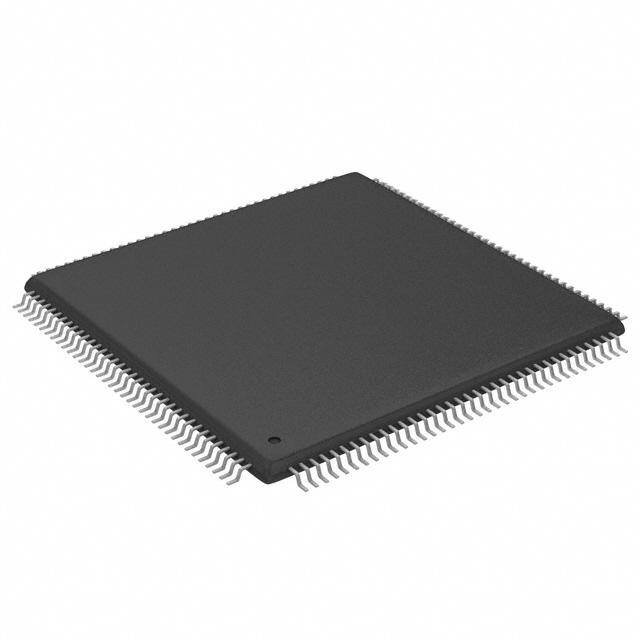
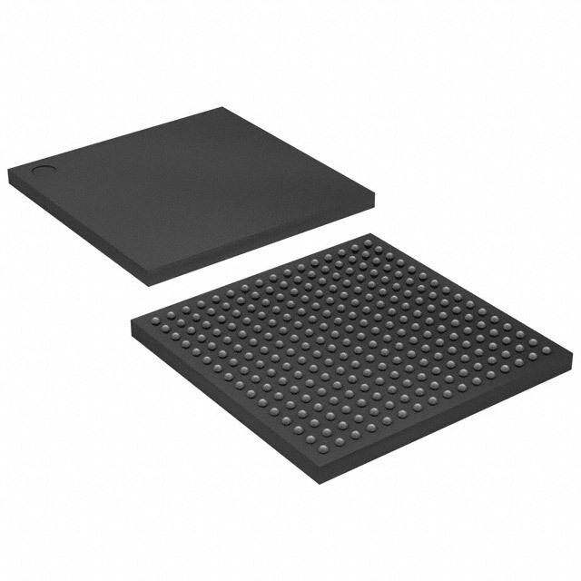
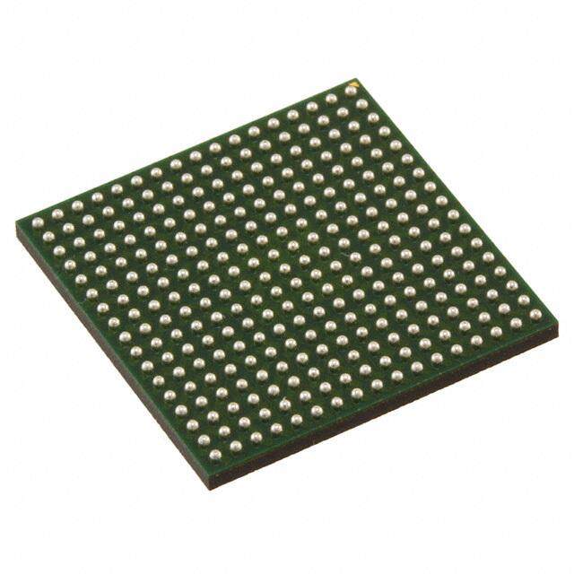
| 描述 | IC FPGA 86 I/O 144TQFP |
| 产品分类 | |
| I/O数 | 86 |
| LAB/CLB数 | 96 |
| 品牌 | Xilinx Inc |
| 数据手册 | |
| 产品图片 |
|
| 产品型号 | XC2S15-5TQ144C |
| PCN设计/规格 | |
| rohs | 含铅 / 不符合限制有害物质指令(RoHS)规范要求 |
| 产品系列 | Spartan®-II |
| 产品目录页面 | |
| 供应商器件封装 | 144-TQFP(20x20) |
| 其它名称 | 122-1218 |
| 安装类型 | 表面贴装 |
| 封装/外壳 | 144-LQFP |
| 工作温度 | 0°C ~ 85°C |
| 总RAM位数 | 16384 |
| 栅极数 | 15000 |
| 标准包装 | 60 |
| 电压-电源 | 2.375 V ~ 2.625 V |
| 逻辑元件/单元数 | 432 |


- 商务部:美国ITC正式对集成电路等产品启动337调查
- 曝三星4nm工艺存在良率问题 高通将骁龙8 Gen1或转产台积电
- 太阳诱电将投资9.5亿元在常州建新厂生产MLCC 预计2023年完工
- 英特尔发布欧洲新工厂建设计划 深化IDM 2.0 战略
- 台积电先进制程称霸业界 有大客户加持明年业绩稳了
- 达到5530亿美元!SIA预计今年全球半导体销售额将创下新高
- 英特尔拟将自动驾驶子公司Mobileye上市 估值或超500亿美元
- 三星加码芯片和SET,合并消费电子和移动部门,撤换高东真等 CEO
- 三星电子宣布重大人事变动 还合并消费电子和移动部门
- 海关总署:前11个月进口集成电路产品价值2.52万亿元 增长14.8%


PDF Datasheet 数据手册内容提取
Spartan-II FPGA Family R Data Sheet DS001 June 13, 2008 Product Specification This document includes all four modules of the Spartan®-II FPGA data sheet. Module 1: Module 3: Introduction and Ordering Information DC and Switching Characteristics DS001-1 (v2.8) June 13, 2008 DS001-3 (v2.8) June 13, 2008 (cid:129) Introduction (cid:129) DC Specifications (cid:129) Features - Absolute Maximum Ratings (cid:129) General Overview - Recommended Operating Conditions - DC Characteristics (cid:129) Product Availability - Power-On Requirements (cid:129) User I/O Chart - DC Input and Output Levels (cid:129) Ordering Information (cid:129) Switching Characteristics Module 2: - Pin-to-Pin Parameters Functional Description - IOB Switching Characteristics - Clock Distribution Characteristics DS001-2 (v2.8) June 13, 2008 - DLL Timing Parameters (cid:129) Architectural Description - CLB Switching Characteristics - Spartan-II Array - Block RAM Switching Characteristics - Input/Output Block - TBUF Switching Characteristics - Configurable Logic Block - JTAG Switching Characteristics - Block RAM Module 4: - Clock Distribution: Delay-Locked Loop Pinout Tables - Boundary Scan (cid:129) Development System DS001-4 (v2.8) June 13, 2008 (cid:129) Configuration (cid:129) Pin Definitions - Configuration Timing (cid:129) Pinout Tables (cid:129) Design Considerations IMPORTANT NOTE: This Spartan-II FPGA data sheet is in four modules. Each module has its own Revision History at the end. Use the PDF "Bookmarks" for easy navigation in this volume. © 2000-2008 Xilinx, Inc. All rights reserved. XILINX, the Xilinx logo, the Brand Window, and other designated brands included herein are trademarks of Xilinx, Inc. All other trademarks are the property of their respective owners. DS001 June 13, 2008 www.xilinx.com Product Specification 1
6 Spartan-II FPGA Family: R Introduction and Ordering Information DS001-1 (v2.8) June 13, 2008 Product Specification 0 Introduction (cid:129) System level features - SelectRAM™ hierarchical memory: The Spartan®-II Field-Programmable Gate Array family · 16 bits/LUT distributed RAM gives users high performance, abundant logic resources, · Configurable 4K bit block RAM and a rich feature set, all at an exceptionally low price. The · Fast interfaces to external RAM six-member family offers densities ranging from 15,000 to - Fully PCI compliant 200,000 system gates, as shown in Table1. System - Low-power segmented routing architecture performance is supported up to 200 MHz. Features include - Full readback ability for verification/observability block RAM (to 56K bits), distributed RAM (to 75,264 bits), - Dedicated carry logic for high-speed arithmetic 16 selectable I/O standards, and four DLLs. Fast, - Efficient multiplier support predictable interconnect means that successive design iterations continue to meet timing requirements. - Cascade chain for wide-input functions - Abundant registers/latches with enable, set, reset The Spartan-II family is a superior alternative to - Four dedicated DLLs for advanced clock control mask-programmed ASICs. The FPGA avoids the initial - Four primary low-skew global clock distribution cost, lengthy development cycles, and inherent risk of nets conventional ASICs. Also, FPGA programmability permits - IEEE 1149.1 compatible boundary scan logic design upgrades in the field with no hardware replacement necessary (impossible with ASICs). (cid:129) Versatile I/O and packaging - Pb-free package options Features - Low-cost packages available in all densities - Family footprint compatibility in common packages (cid:129) Second generation ASIC replacement technology - 16 high-performance interface standards - Densities as high as 5,292 logic cells with up to - Hot swap Compact PCI friendly 200,000 system gates - Zero hold time simplifies system timing - Streamlined features based on Virtex® FPGA architecture (cid:129) Core logic powered at 2.5V and I/Os powered at 1.5V, 2.5V, or 3.3V - Unlimited reprogrammability - Very low cost (cid:129) Fully supported by powerful Xilinx ® ISE® development - Cost-effective 0.18 micron process system - Fully automatic mapping, placement, and routing Table 1: Spartan-II FPGA Family Members CLB Maximum Total Total Logic SystemGates Array Total Available DistributedRAM BlockRAM Device Cells (Logic and RAM) (R x C) CLBs User I/O(1) Bits Bits XC2S15 432 15,000 8 x 12 96 86 6,144 16K XC2S30 972 30,000 12 x 18 216 92 13,824 24K XC2S50 1,728 50,000 16 x 24 384 176 24,576 32K XC2S100 2,700 100,000 20 x 30 600 176 38,400 40K XC2S150 3,888 150,000 24 x 36 864 260 55,296 48K XC2S200 5,292 200,000 28 x 42 1,176 284 75,264 56K Notes: 1. All user I/O counts do not include the four global clock/user input pins. See details in Table2, page4. © 2000-2008 Xilinx, Inc. All rights reserved. XILINX, the Xilinx logo, the Brand Window, and other designated brands included herein are trademarks of Xilinx, Inc. All other trademarks are the property of their respective owners. DS001-1 (v2.8) June 13, 2008 www.xilinx.com Module 1 of 4 Product Specification 2
R Spartan-II FPGA Family: Introduction and Ordering Information General Overview serial mode), or written into the FPGA in slave serial, slave parallel, or Boundary Scan modes. The Spartan-II family of FPGAs have a regular, flexible, programmable architecture of Configurable Logic Blocks Spartan-II FPGAs are typically used in high-volume (CLBs), surrounded by a perimeter of programmable applications where the versatility of a fast programmable Input/Output Blocks (IOBs). There are four Delay-Locked solution adds benefits. Spartan-II FPGAs are ideal for Loops (DLLs), one at each corner of the die. Two columns shortening product development cycles while offering a of block RAM lie on opposite sides of the die, between the cost-effective solution for high volume production. CLBs and the IOB columns. These functional elements are Spartan-II FPGAs achieve high-performance, low-cost interconnected by a powerful hierarchy of versatile routing operation through advanced architecture and channels (see Figure1). semiconductor technology. Spartan-II devices provide Spartan-II FPGAs are customized by loading configuration system clock rates up to 200MHz. In addition to the data into internal static memory cells. Unlimited conventional benefits of high-volume programmable logic reprogramming cycles are possible with this approach. solutions, Spartan-II FPGAs also offer on-chip synchronous Stored values in these cells determine logic functions and single-port and dual-port RAM (block and distributed form), interconnections implemented in the FPGA. Configuration DLL clock drivers, programmable set and reset on all data can be read from an external serial PROM (master flip-flops, fast carry logic, and many other features. DLL DLL M M A A R R K CLBs CLBs K C C O O L L B B M M A A R R K CLBs CLBs K C C O O L L B B DLL DLL I/O LOGIC XC2S15 DS001_01_091800 Figure 1: Basic Spartan-II Family FPGA Block Diagram DS001-1 (v2.8) June 13, 2008 www.xilinx.com Module 1 of 4 Product Specification 3
R Spartan-II FPGA Family: Introduction and Ordering Information Spartan-II Product Availability Table2 shows the maximum user I/Os available on the device and the number of user I/Os available for each device/package combination. The four global clock pins are usable as additional user I/Os when not used as a global clock pin. These pins are not included in user I/O counts. Table 2: Spartan-II FPGA User I/O Chart(1) Available User I/O According to Package Type Maximum VQ100 TQ144 CS144 PQ208 FG256 FG456 Device User I/O VQG100 TQG144 CSG144 PQG208 FGG256 FGG456 XC2S15 86 60 86 (Note 2) - - - XC2S30 92 60 92 92 (Note 2) - - XC2S50 176 - 92 - 140 176 - XC2S100 176 - 92 - 140 176 (Note 2) XC2S150 260 - - - 140 176 260 XC2S200 284 - - - 140 176 284 Notes: 1. All user I/O counts do not include the four global clock/user input pins. 2. Discontinued by PDN2004-01. DS001-1 (v2.8) June 13, 2008 www.xilinx.com Module 1 of 4 Product Specification 4
R Spartan-II FPGA Family: Introduction and Ordering Information Ordering Information Spartan-II devices are available in both standard and Pb-free packaging options for all device/package combinations. The Pb-free packages include a special "G" character in the ordering code. Standard Packaging Example: XC2S50 -6 PQ 208 C Device Type Temperature Range Speed Grade Number of Pins Package Type DS077-1_01a_072204 Pb-Free Packaging Example: XC2S50 -6 PQ G 208 C Device Type Temperature Range Speed Grade Number of Pins Package Type Pb-free DS077-1_01b_072204 Device Ordering Options Device Speed Grade Number of Pins / Package Type Temperature Range (T ) J XC2S15 -5 Standard Performance VQ(G)100 100-pin Plastic Very Thin QFP C = Commercial 0°C to +85°C XC2S30 -6 Higher Performance(1) CS(G)144 144-ball Chip-Scale BGA I = Industrial –40°C to +100°C XC2S50 TQ(G)144 144-pin Plastic Thin QFP XC2S100 PQ(G)208 208-pin Plastic QFP XC2S150 FG(G)256 256-ball Fine Pitch BGA XC2S200 FG(G)456 456-ball Fine Pitch BGA Notes: 1. The -6 speed grade is exclusively available in the Commercial temperature range. Device Part Marking R SPARTANR Device Type XC2S50TM Date Code Package PQ208AFP0025 A1134280A Lot Code Speed 6C Operating Range Sample package with part marking for XC2S50-6PQ208C. ds001-1_02_090303 DS001-1 (v2.8) June 13, 2008 www.xilinx.com Module 1 of 4 Product Specification 5
R Spartan-II FPGA Family: Introduction and Ordering Information Revision History Date Version No. Description 09/18/00 2.0 Sectioned the Spartan-II Family data sheet into four modules. Added industrial temperature range information. 10/31/00 2.1 Removed Power down feature. 03/05/01 2.2 Added statement on PROMs. 11/01/01 2.3 Updated Product Availability chart. Minor text edits. 09/03/03 2.4 Added device part marking. 08/02/04 2.5 Added information on Pb-free packaging options and removed discontinued options. 06/13/08 2.8 Updated description and links. Updated all modules for continuous page, figure, and table numbering. Synchronized all modules to v2.8. PN 011311 DS001-1 (v2.8) June 13, 2008 www.xilinx.com Module 1 of 4 Product Specification 6
50 Spartan-II FPGA Family: R Functional Description DS001-2 (v2.8) June 13, 2008 Product Specification Architectural Description memory elements for easy and quick routing of signals on and off the chip. Spartan-II FPGA Array Values stored in static memory cells control all the The Spartan®-II field-programmable gate array, shown in configurable logic elements and interconnect resources. Figure2, is composed of five major configurable elements: These values load into the memory cells on power-up, and can reload if necessary to change the function of the device. (cid:129) IOBs provide the interface between the package pins and the internal logic Each of these elements will be discussed in detail in the following sections. (cid:129) CLBs provide the functional elements for constructing most logic Input/Output Block (cid:129) Dedicated block RAM memories of 4096 bits each The Spartan-II FPGA IOB, as seen in Figure2, features (cid:129) Clock DLLs for clock-distribution delay compensation inputs and outputs that support a wide variety of I/O and clock domain control signaling standards. These high-speed inputs and outputs (cid:129) Versatile multi-level interconnect structure are capable of supporting various state of the art memory As can be seen in Figure2, the CLBs form the central logic and bus interfaces. Table3 lists several of the standards structure with easy access to all support and routing which are supported along with the required reference, structures. The IOBs are located around all the logic and output and termination voltages needed to meet the standard. T SR V CCO D Q Package TFF Pin CLK CK VCC TCE EC I/O OE Programmable SR Bias & Package Pin ESD Network SR O D Q Programmable OFF Output Buffer CK Internal Reference OCE EC Programmable Delay IQ I/O, VREF SR I D Q Programmable Package Pin Input Buffer IFF CK To Next I/O ICE EC To Other External V Inputs REF of Bank DS001_02_090600 Figure 2: Spartan-II FPGA Input/Output Block (IOB) © 2000-2008 Xilinx, Inc. All rights reserved. XILINX, the Xilinx logo, the Brand Window, and other designated brands included herein are trademarks of Xilinx, Inc. All other trademarks are the property of their respective owners. DS001-2 (v2.8) June 13, 2008 www.xilinx.com Module 2 of 4 Product Specification 7
R Spartan-II FPGA Family: Functional Description The three IOB registers function either as edge-triggered All pads are protected against damage from electrostatic D-type flip-flops or as level-sensitive latches. Each IOB has discharge (ESD) and from over-voltage transients. Two a clock signal (CLK) shared by the three registers and forms of over-voltage protection are provided, one that independent Clock Enable (CE) signals for each register. In permits 5V compliance, and one that does not. For 5V addition to the CLK and CE control signals, the three compliance, a zener-like structure connected to ground registers share a Set/Reset (SR). For each register, this turns on when the output rises to approximately 6.5V. When signal can be independently configured as a synchronous 5V compliance is not required, a conventional clamp diode Set, a synchronous Reset, an asynchronous Preset, or an may be connected to the output supply voltage, V . The CCO asynchronous Clear. type of over-voltage protection can be selected independently for each pad. A feature not shown in the block diagram, but controlled by the software, is polarity control. The input and output buffers All Spartan-II FPGA IOBs support IEEE 1149.1-compatible and all of the IOB control signals have independent polarity boundary scan testing. controls. Input Path Optional pull-up and pull-down resistors and an optional A buffer In the Spartan-II FPGA IOB input path routes the weak-keeper circuit are attached to each pad. Prior to input signal either directly to internal logic or through an configuration all outputs not involved in configuration are optional input flip-flop. forced into their high-impedance state. The pull-down resistors and the weak-keeper circuits are inactive, but An optional delay element at the D-input of this flip-flop inputs may optionally be pulled up. eliminates pad-to-pad hold time. The delay is matched to the internal clock-distribution delay of the FPGA, and when Table 3: Standards Supported by I/O (Typical Values) used, assures that the pad-to-pad hold time is zero. Input Output Board Each input buffer can be configured to conform to any of the Reference Source Termination low-voltage signaling standards supported. In some of Voltage Voltage Voltage these standards the input buffer utilizes a user-supplied I/O Standard (V ) (V ) (V ) REF CCO TT threshold voltage, V . The need to supply V imposes REF REF LVTTL (2-24mA) N/A 3.3 N/A constraints on which standards can used in close proximity to each other. See "I/O Banking," page9. LVCMOS2 N/A 2.5 N/A There are optional pull-up and pull-down resistors at each PCI (3V/5V, N/A 3.3 N/A input for use after configuration. 33 MHz/66 MHz) Output Path GTL 0.8 N/A 1.2 The output path includes a 3-state output buffer that drives GTL+ 1.0 N/A 1.5 the output signal onto the pad. The output signal can be HSTL Class I 0.75 1.5 0.75 routed to the buffer directly from the internal logic or through an optional IOB output flip-flop. HSTL Class III 0.9 1.5 1.5 The 3-state control of the output can also be routed directly HSTL Class IV 0.9 1.5 1.5 from the internal logic or through a flip-flip that provides SSTL3 Class I 1.5 3.3 1.5 synchronous enable and disable. and II Each output driver can be individually programmed for a SSTL2 Class I 1.25 2.5 1.25 wide range of low-voltage signaling standards. Each output and II buffer can source up to 24mA and sink up to 48mA. Drive strength and slew rate controls minimize bus transients. CTT 1.5 3.3 1.5 In most signaling standards, the output high voltage AGP-2X 1.32 3.3 N/A depends on an externally supplied V voltage. The need CCO to supply V imposes constraints on which standards CCO The activation of pull-up resistors prior to configuration is can be used in close proximity to each other. See "I/O controlled on a global basis by the configuration mode pins. Banking". If the pull-up resistors are not activated, all the pins will float. An optional weak-keeper circuit is connected to each Consequently, external pull-up or pull-down resistors must output. When selected, the circuit monitors the voltage on be provided on pins required to be at a well-defined logic the pad and weakly drives the pin High or Low to match the level prior to configuration. input signal. If the pin is connected to a multiple-source signal, the weak keeper holds the signal in its last state if all DS001-2 (v2.8) June 13, 2008 www.xilinx.com Module 2 of 4 Product Specification 8
R Spartan-II FPGA Family: Functional Description drivers are disabled. Maintaining a valid logic level in this automatically configured as inputs for the V voltage. REF way helps eliminate bus chatter. About one in six of the I/O pins in the bank assume this role. Because the weak-keeper circuit uses the IOB input buffer V pins within a bank are interconnected internally and REF to monitor the input level, an appropriate V voltage must consequently only one V voltage can be used within REF REF be provided if the signaling standard requires one. The each bank. All V pins in the bank, however, must be REF provision of this voltage must comply with the I/O banking connected to the external voltage source for correct rules. operation. I/O Banking In a bank, inputs requiring V can be mixed with those REF that do not but only one V voltage may be used within a Some of the I/O standards described above require V REF CCO bank. Input buffers that use V are not 5V tolerant. and/or V voltages. These voltages are externally REF REF LVTTL, LVCMOS2, and PCI are 5V tolerant. The V and connected to device pins that serve groups of IOBs, called CCO V pins for each bank appear in the device pinout tables. banks. Consequently, restrictions exist about which I/O REF standards can be combined within a given bank. Within a given package, the number of V and V pins REF CCO can vary depending on the size of device. In larger devices, Eight I/O banks result from separating each edge of the more I/O pins convert to V pins. Since these are always FPGA into two banks (see Figure3). Each bank has REF a superset of the V pins used for smaller devices, it is multiple V pins which must be connected to the same REF CCO possible to design a PCB that permits migration to a larger voltage. Voltage is determined by the output standards in device. All V pins for the largest device anticipated must use. REF be connected to the V voltage, and not used for I/O. REF Independent Banks Available Package VQ100 CS144 FG256 Bank 0 Bank 1 PQ208 TQ144 FG456 7 2 nk GCLK3 GCLK2 nk Independent Banks 1 4 8 a a B B Configurable Logic Block Spartan-II Device The basic building block of the Spartan-II FPGA CLB is the logic cell (LC). An LC includes a 4-input function generator, 6 3 carry logic, and storage element. Output from the function k k an GCLK1 GCLK0 an generator in each LC drives the CLB output and the Dinput B B of the flip-flop. Each Spartan-II FPGA CLB contains four Bank 5 Bank 4 LCs, organized in two similar slices; a single slice is shown in Figure4. In addition to the four basic LCs, the Spartan-II FPGA CLB DS001_03_060100 Figure 3: Spartan-II I/O Banks contains logic that combines function generators to provide functions of five or six inputs. Within a bank, output standards may be mixed only if they Look-Up Tables use the same V . Compatible standards are shown in CCO Table4. GTL and GTL+ appear under all voltages because Spartan-II FPGA function generators are implemented as their open-drain outputs do not depend on V . 4-input look-up tables (LUTs). In addition to operating as a CCO function generator, each LUT can provide a 16x1-bit Table 4: Compatible Output Standards synchronous RAM. Furthermore, the two LUTs within a V Compatible Standards slice can be combined to create a 16x2-bit or 32x1-bit CCO synchronous RAM, or a 16x1-bit dual-port synchronous 3.3V PCI, LVTTL, SSTL3 I, SSTL3 II, CTT, AGP, RAM. GTL, GTL+ The Spartan-II FPGA LUT can also provide a 16-bit shift 2.5V SSTL2 I, SSTL2 II, LVCMOS2, GTL, GTL+ register that is ideal for capturing high-speed or burst-mode 1.5V HSTL I, HSTL III, HSTL IV, GTL, GTL+ data. This mode can also be used to store data in applications such as Digital Signal Processing. Some input standards require a user-supplied threshold voltage, V . In this case, certain user-I/O pins are REF DS001-2 (v2.8) June 13, 2008 www.xilinx.com Module 2 of 4 Product Specification 9
R Spartan-II FPGA Family: Functional Description COUT YB Y G4 I4 S Look-Up D Q YQ Table G3 I3 Carry O and CK G2 I2 Control Logic EC G1 I1 R F5IN BY SR XB X F4 I4 S Look-Up D Q XQ Table F3 I3 Carry O and CK F2 I2 Control Logic EC F1 I1 R BX CIN CLK CE DS001_04_091400 Figure 4: Spartan-II CLB Slice (two identical slices in each CLB) Storage Elements opposite state. Alternatively, these signals may be configured to operate asynchronously. Storage elements in the Spartan-II FPGA slice can be configured either as edge-triggered D-type flip-flops or as All control signals are independently invertible, and are level-sensitive latches. The D inputs can be driven either by shared by the two flip-flops within the slice. function generators within the slice or directly from slice Additional Logic inputs, bypassing the function generators. The F5 multiplexer in each slice combines the function In addition to Clock and Clock Enable signals, each slice generator outputs. This combination provides either a has synchronous set and reset signals (SR and BY). SR function generator that can implement any 5-input function, forces a storage element into the initialization state a 4:1 multiplexer, or selected functions of up to nine inputs. specified for it in the configuration. BY forces it into the DS001-2 (v2.8) June 13, 2008 www.xilinx.com Module 2 of 4 Product Specification 10
R Spartan-II FPGA Family: Functional Description Similarly, the F6 multiplexer combines the outputs of all four Each block RAM cell, as illustrated in Figure5, is a fully function generators in the CLB by selecting one of the synchronous dual-ported 4096-bit RAM with independent F5-multiplexer outputs. This permits the implementation of control signals for each port. The data widths of the two any 6-input function, an 8:1 multiplexer, or selected ports can be configured independently, providing built-in functions of up to 19 inputs. bus-width conversion. Each CLB has four direct feedthrough paths, one per LC. RAMB4_S#_S# These paths provide extra data input lines or additional local routing that does not consume logic resources. WEA ENA Arithmetic Logic RSTA DOA[#:0] Dedicated carry logic provides capability for high-speed CLKA arithmetic functions. The Spartan-II FPGA CLB supports ADD[#:0] two separate carry chains, one per slice. The height of the DIA[#:0] carry chains is two bits per CLB. The arithmetic logic includes an XOR gate that allows a WEB 1-bit full adder to be implemented within an LC. In addition, ENB a dedicated AND gate improves the efficiency of multiplier RSTB DOB[#:0] CLKB implementation. ADDRB[#:0] The dedicated carry path can also be used to cascade DIB[#:0] function generators for implementing wide logic functions. DS001_05_060100 BUFTs Figure 5: Dual-Port Block RAM Each Spartan-II FPGA CLB contains two 3-state drivers Table6 shows the depth and width aspect ratios for the (BUFTs) that can drive on-chip busses. See "Dedicated block RAM. Routing," page12. Each Spartan-II FPGA BUFT has an independent 3-state control pin and an independent input Table 6: Block RAM Port Aspect Ratios pin. Width Depth ADDR Bus Data Bus Block RAM 1 4096 ADDR<11:0> DATA<0> Spartan-II FPGAs incorporate several large block RAM 2 2048 ADDR<10:0> DATA<1:0> memories. These complement the distributed RAM 4 1024 ADDR<9:0> DATA<3:0> Look-Up Tables (LUTs) that provide shallow memory structures implemented in CLBs. 8 512 ADDR<8:0> DATA<7:0> Block RAM memory blocks are organized in columns. All 16 256 ADDR<7:0> DATA<15:0> Spartan-II devices contain two such columns, one along each vertical edge. These columns extend the full height of The Spartan-II FPGA block RAM also includes dedicated the chip. Each memory block is four CLBs high, and routing to provide an efficient interface with both CLBs and consequently, a Spartan-II device eight CLBs high will other block RAMs. contain two memory blocks per column, and a total of four blocks. Programmable Routing Matrix Table 5: Spartan-II Block RAM Amounts It is the longest delay path that limits the speed of any worst-case design. Consequently, the Spartan-II routing Spartan-II Total Block RAM architecture and its place-and-route software were defined Device # of Blocks Bits in a single optimization process. This joint optimization XC2S15 4 16K minimizes long-path delays, and consequently, yields the best system performance. XC2S30 6 24K The joint optimization also reduces design compilation XC2S50 8 32K times because the architecture is software-friendly. Design XC2S100 10 40K cycles are correspondingly reduced due to shorter design iteration times. XC2S150 12 48K XC2S200 14 56K DS001-2 (v2.8) June 13, 2008 www.xilinx.com Module 2 of 4 Product Specification 11
R Spartan-II FPGA Family: Functional Description Local Routing efficiently. Vertical Longlines span the full height of the device, and horizontal ones span the full width of the The local routing resources, as shown in Figure6, provide device. the following three types of connections: I/O Routing (cid:129) Interconnections among the LUTs, flip-flops, and General Routing Matrix (GRM) Spartan-II devices have additional routing resources (cid:129) Internal CLB feedback paths that provide high-speed around their periphery that form an interface between the connections to LUTs within the same CLB, chaining CLB array and the IOBs. This additional routing, called the them together with minimal routing delay VersaRing, facilitates pin-swapping and pin-locking, such that logic redesigns can adapt to existing PCB layouts. (cid:129) Direct paths that provide high-speed connections Time-to-market is reduced, since PCBs and other system between horizontally adjacent CLBs, eliminating the components can be manufactured while the logic design is delay of the GRM still in progress. To Adjacent Dedicated Routing GRM Some classes of signal require dedicated routing resources to maximize performance. In the Spartan-II architecture, To Adjacent To Adjacent dedicated routing resources are provided for two classes of GRM GRM GRM signal. (cid:129) Horizontal routing resources are provided for on-chip 3-state busses. Four partitionable bus lines are To Adjacent provided per CLB row, permitting multiple busses GRM within a row, as shown in Figure7. Direct Connection Direct To Adjacent CLB Connection (cid:129) Two dedicated nets per CLB propagate carry signals CLB To Adjacent vertically to the adjacent CLB. CLB Global Routing DS001_06_032300 Figure 6: Spartan-II Local Routing Global Routing resources distribute clocks and other signals with very high fanout throughout the device. General Purpose Routing Spartan-II devices include two tiers of global routing resources referred to as primary and secondary global Most Spartan-II FPGA signals are routed on the general routing resources. purpose routing, and consequently, the majority of interconnect resources are associated with this level of the (cid:129) The primary global routing resources are four routing hierarchy. The general routing resources are dedicated global nets with dedicated input pins that are located in horizontal and vertical routing channels designed to distribute high-fanout clock signals with associated with the rows and columns CLBs. The minimal skew. Each global clock net can drive all CLB, general-purpose routing resources are listed below. IOB, and block RAM clock pins. The primary global nets may only be driven by global buffers. There are (cid:129) Adjacent to each CLB is a General Routing Matrix four global buffers, one for each global net. (GRM). The GRM is the switch matrix through which (cid:129) The secondary global routing resources consist of 24 horizontal and vertical routing resources connect, and backbone lines, 12 across the top of the chip and 12 is also the means by which the CLB gains access to across bottom. From these lines, up to 12 unique the general purpose routing. signals per column can be distributed via the 12 (cid:129) 24 single-length lines route GRM signals to adjacent longlines in the column. These secondary resources GRMs in each of the four directions. are more flexible than the primary resources since they (cid:129) 96 buffered Hex lines route GRM signals to other are not restricted to routing only to clock pins. GRMs six blocks away in each one of the four directions. Organized in a staggered pattern, Hex lines may be driven only at their endpoints. Hex-line signals can be accessed either at the endpoints or at the midpoint (three blocks from the source). One third of the Hex lines are bidirectional, while the remaining ones are unidirectional. (cid:129) 12 Longlines are buffered, bidirectional wires that distribute signals across the device quickly and DS001-2 (v2.8) June 13, 2008 www.xilinx.com Module 2 of 4 Product Specification 12
R Spartan-II FPGA Family: Functional Description 3-State Lines CLB CLB CLB CLB DS001_07_090600 Figure 7: BUFT Connections to Dedicated Horizontal Bus Lines Clock Distribution networks. The DLL monitors the input clock and the distributed clock, and automatically adjusts a clock delay The Spartan-II family provides high-speed, low-skew clock element. Additional delay is introduced such that clock distribution through the primary global routing resources edges reach internal flip-flops exactly one clock period after described above. A typical clock distribution net is shown in they arrive at the input. This closed-loop system effectively Figure8. eliminates clock-distribution delay by ensuring that clock Four global buffers are provided, two at the top center of the edges arrive at internal flip-flops in synchronism with clock device and two at the bottom center. These drive the four edges arriving at the input. primary global nets that in turn drive any clock pin. In addition to eliminating clock-distribution delay, the DLL Four dedicated clock pads are provided, one adjacent to provides advanced control of multiple clock domains. The each of the global buffers. The input to the global buffer is DLL provides four quadrature phases of the source clock, selected either from these pads or from signals in the can double the clock, or divide the clock by 1.5, 2, 2.5, 3, 4, general purpose routing. Global clock pins do not have the 5, 8, or 16. It has six outputs. option for internal, weak pull-up resistors. The DLL also operates as a clock mirror. By driving the output from a DLL off-chip and then back on again, the DLL Global GCLKPAD3 GCLKPAD2 can be used to deskew a board level clock among multiple Clock Rows GCLKBUF3 GCLKBUF2 Global Clock Spartan-II devices. Column In order to guarantee that the system clock is operating correctly prior to the FPGA starting up after configuration, the DLL can delay the completion of the configuration process until after it has achieved lock. Boundary Scan Global Clock Spine Spartan-II devices support all the mandatory boundary- scan instructions specified in the IEEE standard 1149.1. A Test Access Port (TAP) and registers are provided that implement the EXTEST, SAMPLE/PRELOAD, and BYPASS instructions. The TAP also supports two USERCODE instructions and internal scan chains. GCLKBUF1 GCLKBUF0 GCLKPAD1 GCLKPAD0 The TAP uses dedicated package pins that always operate DS001_08_060100 using LVTTL. For TDO to operate using LVTTL, the V Figure 8: Global Clock Distribution Network CCO for Bank 2 must be 3.3V. Otherwise, TDO switches rail-to-rail between ground and V . TDI, TMS, and TCK CCO Delay-Locked Loop (DLL) have a default internal weak pull-up resistor, and TDO has no default resistor. Bitstream options allow setting any of Associated with each global clock input buffer is a fully the four TAP pins to have an internal pull-up, pull-down, or digital Delay-Locked Loop (DLL) that can eliminate skew neither. between the clock input pad and internal clock-input pins throughout the device. Each DLL can drive two global clock DS001-2 (v2.8) June 13, 2008 www.xilinx.com Module 2 of 4 Product Specification 13
R Spartan-II FPGA Family: Functional Description Boundary-scan operation is independent of individual IOB The public boundary-scan instructions are available prior to configurations, and unaffected by package type. All IOBs, configuration. After configuration, the public instructions including unbonded ones, are treated as independent remain available together with any USERCODE 3-state bidirectional pins in a single scan chain. Retention of instructions installed during the configuration. While the the bidirectional test capability after configuration facilitates SAMPLE and BYPASS instructions are available during the testing of external interconnections. configuration, it is recommended that boundary-scan operations not be performed during this transitional period. Table7 lists the boundary-scan instructions supported in Spartan-II FPGAs. Internal signals can be captured during In addition to the test instructions outlined above, the EXTEST by connecting them to unbonded or unused IOBs. boundary-scan circuitry can be used to configure the FPGA, They may also be connected to the unused outputs of IOBs and also to read back the configuration data. defined as unidirectional input pins. To facilitate internal scan chains, the User Register Table 7: Boundary-Scan Instructions provides three outputs (Reset, Update, and Shift) that represent the corresponding states in the boundary-scan Boundary-Scan Binary internal state machine. Command Code[4:0] Description EXTEST 00000 Enables boundary-scan EXTEST operation SAMPLE 00001 Enables boundary-scan SAMPLE operation USR1 00010 Access user-defined register 1 USR2 00011 Access user-defined register 2 CFG_OUT 00100 Access the configuration bus for Readback CFG_IN 00101 Access the configuration bus for Configuration INTEST 00111 Enables boundary-scan INTEST operation USRCODE 01000 Enables shifting out USER code IDCODE 01001 Enables shifting out of ID Code HIZ 01010 Disables output pins while enabling the Bypass Register JSTART 01100 Clock the start-up sequence when StartupClk is TCK BYPASS 11111 Enables BYPASS RESERVED All other Xilinx® reserved codes instructions DS001-2 (v2.8) June 13, 2008 www.xilinx.com Module 2 of 4 Product Specification 14
R Spartan-II FPGA Family: Functional Description Figure9 is a diagram of the Spartan-II family boundary scan logic. It includes three bits of Data Register per IOB, the IEEE 1149.1 Test Access Port controller, and the Instruction Register with decodes. DATA IN IOB.T 0 1 sd D Q D Q 1 0 IOB IOB IOB IOB IOB LE IOB IOB 1 sd D Q D Q 0 IOB IOB LE IOB IOB 1 IOB.I IOB IOB 0 1 sd IOB IOB D Q D Q 0 IOB IOB LE 1 IOB Bypass IOB IOB.Q 0 Register IOB.T 0 M TDO TDI Instruction Register UX 10 D Q D sd Q 1 LE 1 sd D Q D Q 0 LE 1 IOB.I 0 DATAOUT UPDATE EXTEST SHIFT/ CLOCK DATA CAPTURE REGISTER DS001_09_032300 Figure 9: Spartan-II Family Boundary Scan Logic Bit Sequence The bit sequence within each IOB is: In, Out, 3-State. The input-only pins contribute only the In bit to the boundary scan I/O data register, while the output-only pins contributes all three bits. From a cavity-up view of the chip (as shown in the FPGA Editor), starting in the upper right chip corner, the boundary scan data-register bits are ordered as shown in Figure10. BSDL (Boundary Scan Description Language) files for Spartan-II family devices are available on the Xilinx website, in the Downloads area. DS001-2 (v2.8) June 13, 2008 www.xilinx.com Module 2 of 4 Product Specification 15
R Spartan-II FPGA Family: Functional Description Design Implementation Bit 0 ( TDO end) TDO.T The place-and-route tools (PAR) automatically provide the Bit 1 TDO.O implementation flow described in this section. The Bit 2 Top-edge IOBs (Right to Left) partitioner takes the EDIF netlist for the design and maps the logic into the architectural resources of the FPGA (CLBs and IOBs, for example). The placer then determines the Left-edge IOBs (Top to Bottom) best locations for these blocks based on their interconnections and the desired performance. Finally, the MODE.I router interconnects the blocks. The PAR algorithms support fully automatic implementation of most designs. For demanding applications, however, the Bottom-edge IOBs (Left to Right) user can exercise various degrees of control over the process. User partitioning, placement, and routing Right-edge IOBs (Bottom to Top) information is optionally specified during the design-entry (TDI end) BSCANT.UPD process. The implementation of highly structured designs can benefit greatly from basic floorplanning. DS001_10_032300 Figure 10: Boundary Scan Bit Sequence The implementation software incorporates timing-driven placement and routing. Designers specify timing Development System requirements along entire paths during design entry. The timing path analysis routines in PAR then recognize these Spartan-II FPGAs are supported by the Xilinx ISE® user-specified requirements and accommodate them. development tools. The basic methodology for Spartan-II FPGA design consists of three interrelated steps: design Timing requirements are entered in a form directly relating entry, implementation, and verification. Industry-standard to the system requirements, such as the targeted clock tools are used for design entry and simulation, while Xilinx frequency, or the maximum allowable delay between two provides proprietary architecture-specific tools for registers. In this way, the overall performance of the system implementation. along entire signal paths is automatically tailored to user-generated specifications. Specific timing information The Xilinx development system is integrated under a single for individual nets is unnecessary. graphical interface, providing designers with a common user interface regardless of their choice of entry and Design Verification verification tools. The software simplifies the selection of implementation options with pull-down menus and on-line In addition to conventional software simulation, FPGA users help. can use in-circuit debugging techniques. Because Xilinx devices are infinitely reprogrammable, designs can be For HDL design entry, the Xilinx FPGA development verified in real time without the need for extensive sets of system provides interfaces to several synthesis design software simulation vectors. environments. The development system supports both software simulation A standard interface-file specification, Electronic Design and in-circuit debugging techniques. For simulation, the Interchange Format (EDIF), simplifies file transfers into and system extracts the post-layout timing information from the out of the development system. design database, and back-annotates this information into Spartan-II FPGAs supported by a unified library of standard the netlist for use by the simulator. Alternatively, the user functions. This library contains over 400 primitives and can verify timing-critical portions of the design using the macros, ranging from 2-input AND gates to 16-bit static timing analyzer. accumulators, and includes arithmetic functions, For in-circuit debugging, the development system includes comparators, counters, data registers, decoders, encoders, a download cable, which connects the FPGA in the target I/O functions, latches, Boolean functions, multiplexers, shift system to a PC or workstation. After downloading the registers, and barrel shifters. design into the FPGA, the designer can read back the The design environment supports hierarchical design entry. contents of the flip-flops, and so observe the internal logic These hierarchical design elements are automatically state. Simple modifications can be downloaded into the combined by the implementation tools. Different design system in a matter of minutes. entry tools can be combined within a hierarchical design, thus allowing the most convenient entry method to be used for each portion of the design. DS001-2 (v2.8) June 13, 2008 www.xilinx.com Module 2 of 4 Product Specification 16
R Spartan-II FPGA Family: Functional Description Configuration Table 8: Spartan-II Configuration File Size Configuration is the process by which the bitstream of a design, as generated by the Xilinx software, is loaded into Device Configuration File Size (Bits) the internal configuration memory of the FPGA. Spartan-II XC2S15 197,696 devices support both serial configuration, using the master/slave serial and JTAG modes, as well as byte-wide XC2S30 336,768 configuration employing the Slave Parallel mode. XC2S50 559,200 Configuration File XC2S100 781,216 Spartan-II devices are configured by sequentially loading XC2S150 1,040,096 frames of data that have been concatenated into a XC2S200 1,335,840 configuration file. Table8 shows how much nonvolatile storage space is needed for Spartan-II devices. Modes It is important to note that, while a PROM is commonly used Spartan-II devices support the following four configuration to store configuration data before loading them into the modes: FPGA, it is by no means required. Any of a number of different kinds of under populated nonvolatile storage (cid:129) Slave Serial mode already available either on or off the board (i.e., hard drives, (cid:129) Master Serial mode FLASH cards, etc.) can be used. For more information on (cid:129) Slave Parallel mode configuration without a PROM, refer to XAPP098, The Low-Cost, Efficient Serial Configuration of Spartan FPGAs. (cid:129) Boundary-scan mode The Configuration mode pins (M2, M1, M0) select among these configuration modes with the option in each case of having the IOB pins either pulled up or left floating prior to the end of configuration. The selection codes are listed in Table9. Configuration through the boundary-scan port is always available, independent of the mode selection. Selecting the boundary-scan mode simply turns off the other modes. The three mode pins have internal pull-up resistors, and default to a logic High if left unconnected. Table 9: Configuration Modes Preconfiguration CCLK Configuration Mode Pull-ups M0 M1 M2 Direction Data Width Serial D OUT Master Serial mode No 0 0 0 Out 1 Yes Yes 0 0 1 Slave Parallel mode Yes 0 1 0 In 8 No No 0 1 1 Boundary-Scan mode Yes 1 0 0 N/A 1 No No 1 0 1 Slave Serial mode Yes 1 1 0 In 1 Yes No 1 1 1 Notes: 1. During power-on and throughout configuration, the I/O drivers will be in a high-impedance state. After configuration, all unused I/Os (those not assigned signals) will remain in a high-impedance state. Pins used as outputs may pulse High at the end of configuration (see Answer 10504). 2. If the Mode pins are set for preconfiguration pull-ups, those resistors go into effect once the rising edge of INIT samples the Mode pins. They will stay in effect until GTS is released during startup, after which the UnusedPin bitstream generator option will determine whether the unused I/Os have a pull-up, pull-down, or no resistor. DS001-2 (v2.8) June 13, 2008 www.xilinx.com Module 2 of 4 Product Specification 17
R Spartan-II FPGA Family: Functional Description Signals by driving DONE Low, then enters the memory-clearing phase. There are two kinds of pins that are used to configure Spartan-IIdevices: Dedicated pins perform only specific configuration-related functions; the other pins can serve as Configuration Configuration During general purpose I/Os once user operation has begun. at Power-up User Operation The dedicated pins comprise the mode pins (M2, M1, M0), the configuration clock pin (CCLK), the PROGRAM pin, the DONE pin and the boundary-scan pins (TDI, TDO, TMS, VCCO No AND User Pulls TCK). Depending on the selected configuration mode, VCCINT PROGRAM CCLK may be an output generated by the FPGA, or may be High? Low generated externally, and provided to the FPGA as an Yes input. Note that some configuration pins can act as outputs. For correct operation, these pins require a V of 3.3V to drive CCO FPGA an LVTTL signal or 2.5V to drive an LVCMOS signal. All the Drives INIT relevant pins fall in banks 2 or3. The CS and WRITE pins and DONE Low for Slave Parallel mode are located in bank 1. For a more detailed description than that given below, see Clear "Pinout Tables" in Module 4 and XAPP176, Spartan-II Delay Configuration Configuration FPGA Series Configuration and Readback. Memory The Process The sequence of steps necessary to configure Spartan-II User Holding Yes devices are shown in Figure11. The overall flow can be PROGRAM Low? divided into three different phases. No (cid:129) Initiating Configuration Delay (cid:129) Configuration memory clear Configuration User Holding Yes (cid:129) Loading data frames INIT (cid:129) Start-up Low? The memory clearing and start-up phases are the same for No all configuration modes; however, the steps for the loading FPGA of data frames are different. Thus, the details for data frame Samples loading are described separately in the sections devoted to Mode Pins each mode. Initiating Configuration Load Configuration There are two different ways to initiate the configuration Data Frames process: applying power to the device or asserting the PROGRAM input. Configuration on power-up occurs automatically unless it is CRC No FPGA Drives INIT Low delayed by the user, as described in a separate section Correct? Abort Start-up below. The waveform for configuration on power-up is shown in Figure12, page19. Before configuration can Yes begin, V Bank 2 must be greater than 1.0V. CCO Start-up Sequence Furthermore, all VCCINT power pins must be connected to a FPGA Drives DONE High, 2.5V supply. For more information on delaying Activates I/Os, configuration, see "Clearing Configuration Memory," Releases GSR net page19. Once in user operation, the device can be re-configured User Operation simply by pulling the PROGRAM pin Low. The device DS001_11_111501 acknowledges the beginning of the configuration process Figure 11: Configuration Flow Diagram DS001-2 (v2.8) June 13, 2008 www.xilinx.com Module 2 of 4 Product Specification 18
R Spartan-II FPGA Family: Functional Description VCC(1) TPOR PROGRAM TPL INIT TICCK CCLK Output or Input M0, M1, M2 Valid (Required) DS001_12_102301 . Symbol Description Min Max T Power-on reset - 2 ms POR T Program latency - 100 μs PL T CCLK output delay (Master Serial mode only) 0.5 μs 4 μs ICCK T Program pulse width 300 ns - PROGRAM Notes: (referring to waveform above:) 1. Before configuration can begin, V must be greater than 1.6V and V Bank 2 must be greater than 1.0V. CCINT CCO Figure 12: Configuration Timing on Power-Up Clearing Configuration Memory do not match, the FPGA drives INIT Low to indicate that a frame error has occurred and configuration is aborted. The device indicates that clearing the configuration memory is in progress by driving INIT Low. At this time, the user can To reconfigure the device, the PROGRAM pin should be delay configuration by holding either PROGRAM or INIT asserted to reset the configuration logic. Recycling power Low, which causes the device to remain in the memory also resets the FPGA for configuration. See "Clearing clearing phase. Note that the bidirectional INIT line is Configuration Memory". driving a Low logic level during memory clearing. To avoid Start-up contention, use an open-drain driver to keep INIT Low. The start-up sequence oversees the transition of the FPGA With no delay in force, the device indicates that the memory from the configuration state to full user operation. A match is completely clear by driving INIT High. The FPGA samples of CRC values, indicating a successful loading of the its mode pins on this Low-to-High transition. configuration data, initiates the sequence. Loading Configuration Data During start-up, the device performs four operations: Once INIT is High, the user can begin loading configuration 1. The assertion of DONE. The failure of DONE to go High data frames into the device. The details of loading the may indicate the unsuccessful loading of configuration configuration data are discussed in the sections treating the data. configuration modes individually. The sequence of 2. The release of the Global Three State net. This operations necessary to load configuration data using the activates I/Os to which signals are assigned. The serial modes is shown in Figure14. Loading data using the remaining I/Os stay in a high-impedance state with Slave Parallel mode is shown in Figure19, page25. internal weak pull-down resistors present. CRC Error Checking 3. Negates Global Set Reset (GSR). This allows all During the loading of configuration data, a CRC value flip-flops to change state. embedded in the configuration file is checked against a 4. The assertion of Global Write Enable (GWE). This CRC value calculated within the FPGA. If the CRC values allows all RAMs and flip-flops to change state. DS001-2 (v2.8) June 13, 2008 www.xilinx.com Module 2 of 4 Product Specification 19
R Spartan-II FPGA Family: Functional Description By default, these operations are synchronized to CCLK. Serial Modes The entire start-up sequence lasts eight cycles, called There are two serial configuration modes: In Master Serial C0-C7, after which the loaded design is fully functional. The mode, the FPGA controls the configuration process by default timing for start-up is shown in the top half of driving CCLK as an output. In Slave Serial mode, the FPGA Figure13. The four operations can be selected to switch on passively receives CCLK as an input from an external agent any CCLK cycle C1-C6 through settings in the Xilinx (e.g., a microprocessor, CPLD, or second FPGA in master software. Heavy lines show default settings. mode) that is controlling the configuration process. In both modes, the FPGA is configured by loading one bit per Default Cycles CCLK cycle. The MSB of each configuration data byte is Start-up CLK always written to the DIN pin first. See Figure14 for the sequence for loading data into the Phase 0 1 2 3 4 5 6 7 Spartan-II FPGA serially. This is an expansion of the "Load Configuration Data Frames" block in Figure11. Note that DONE CS and WRITE normally are not used during serial configuration. To ensure successful loading of the FPGA, GTS do not toggle WRITE with CS Low during serial configuration. GSR After INIT GWE Goes High Sync to DONE User Load One Configuration Start-up CLK Bit on Next CCLK Rising Edge Phase 0 1 2 3 4 5 6 7 End of No Configuration DONE High Data File? Yes DONE To CRC Check GTS DS001_14_042403 Figure 14: Loading Serial Mode Configuration Data GSR GWE DS001_13_090600 Figure 13: Start-Up Waveforms The bottom half of Figure13 shows another commonly used version of the start-up timing known as Sync-to-DONE. This version makes the GTS, GSR, and GWE events conditional upon the DONE pin going High. This timing is important for a daisy chain of multiple FPGAs in serial mode, since it ensures that all FPGAs go through start-up together, after all their DONE pins have gone High. Sync-to-DONE timing is selected by setting the GTS, GSR, and GWE cycles to a value of DONE in the configuration options. This causes these signals to transition one clock cycle after DONE externally transitions High. DS001-2 (v2.8) June 13, 2008 www.xilinx.com Module 2 of 4 Product Specification 20
R Spartan-II FPGA Family: Functional Description Slave Serial Mode Multiple FPGAs in Slave Serial mode can be daisy-chained for configuration from a single source. The maximum In Slave Serial mode, the FPGA’s CCLK pin is driven by an amount of data that can be sent to the DOUT pin for a serial external source, allowing FPGAs to be configured from daisy chain is 220-1 (1,048,575) 32-bit words, or 33,554,400 other logic devices such as microprocessors or in a bits, which is approximately 25 XC2S200 bitstreams. The daisy-chain configuration. Figure15 shows connections for configuration bitstream of downstream devices is limited to a Master Serial FPGA configuring a Slave Serial FPGA this size. from a PROM. A Spartan-II device in slave serial mode should be connected as shown for the third device from the After an FPGA is configured, data for the next device is left. Slave Serial mode is selected by a <11x> on the mode routed to the DOUT pin. Data on the DOUT pin changes on pins (M0, M1, M2). the rising edge of CCLK. Configuration must be delayed until INIT pins of all daisy-chained FPGAs are High. For Figure16 shows the timing for Slave Serial configuration. more information, see "Start-up," page19. The serial bitstream must be setup at the DIN input pin a short time before each rising edge of an externally generated CCLK. 3.3V 2.5V 3.3V 3.3V 3.3V 2.5V M0 M1 VCCO 3.3 K M0 M1 VCCO M2 VCCINT M2 VCCINT DOUT DIN DOUT CCLK Spartan-II Spartan-II (Master Serial) (Slave) Vcc CCLK CLK PROM DIN DATA PROGRAM CE CEO PROGRAM DONE INIT RESET/OE DONE INIT GND GND GND PROGRAM DS001_15_060608 Notes: 1. If the DriveDone configuration option is not active for any of the FPGAs, pull up DONE with a 330Ω resistor. Figure 15: Master/Slave Serial Configuration Circuit Diagram DS001-2 (v2.8) June 13, 2008 www.xilinx.com Module 2 of 4 Product Specification 21
R Spartan-II FPGA Family: Functional Description DIN TDCC TCCD TCCL CCLK TCCH TCCO DOUT (Output) DS001_16_032300 . Symbol Description Units T DIN setup 5 ns, min DCC T DIN hold 0 ns, min CCD T DOUT 12 ns, max CCO CCLK T High time 5 ns, min CCH T Low time 5 ns, min CCL F Maximum frequency 66 MHz, max CC Figure 16: Slave Serial Mode Timing DS001-2 (v2.8) June 13, 2008 www.xilinx.com Module 2 of 4 Product Specification 22
R Spartan-II FPGA Family: Functional Description Master Serial Mode the configuration data are being loaded, the CCLK frequency is always 2.5MHz. This frequency is used until In Master Serial mode, the CCLK output of the FPGA drives the ConfigRate bits, part of the configuration file, have been a Xilinx PROM which feeds a serial stream of configuration loaded into the FPGA, at which point, the frequency data to the FPGA’s DIN input. Figure15 shows a Master changes to the selected ConfigRate. Unless a different Serial FPGA configuring a Slave Serial FPGA from a frequency is specified in the design, the default ConfigRate PROM. A Spartan-II device in Master Serial mode should is 4MHz. The frequency of the CCLK signal created by the be connected as shown for the device on the left side. internal oscillator has a variance of +45%, –30% from the Master Serial mode is selected by a <00x> on the mode specified value. pins (M0, M1, M2). The PROM RESET pin is driven by INIT, and CE input is driven by DONE. The interface is identical Figure17 shows the timing for Master Serial configuration. to the slave serial mode except that an oscillator internal to The FPGA accepts one bit of configuration data on each the FPGA is used to generate the configuration clock rising CCLK edge. After the FPGA has been loaded, the (CCLK). Any of a number of different frequencies ranging data for the next device in a daisy-chain is presented on the from 4 to 60 MHz can be set using the ConfigRate option in DOUT pin after the rising CCLK edge. the Xilinx software. On power-up, while the first 60 bytes of CCLK (Output) TCKDS TDSCK Serial Data In TCCO Serial DOUT (Output) DS001_17_110101 . Symbol Description Units T DIN setup 5.0 ns, min DSCK T DIN hold 0.0 ns, min CKDS CCLK Frequency tolerance with respect to +45%, –30% - nominal Figure 17: Master Serial Mode Timing Slave Parallel Mode The agent controlling configuration is not shown. Typically, a processor, a microcontroller, or CPLD controls the Slave The Slave Parallel mode is the fastest configuration option. Parallel interface. The controlling agent provides byte-wide Byte-wide data is written into the FPGA. A BUSY flag is configuration data, CCLK, a Chip Select (CS) signal and a provided for controlling the flow of data at a clock frequency Write signal (WRITE). If BUSY is asserted (High) by the F above 50 MHz. CCNH FPGA, the data must be held until BUSY goes Low. Figure18, page24 shows the connections for two After configuration, the pins of the Slave Parallel port Spartan-IIdevices using the Slave Parallel mode. Slave (D0-D7) can be used as additional user I/O. Alternatively, Parallel mode is selected by a <011> on the mode pins (M0, the port may be retained to permit high-speed 8-bit M1, M2). readback. Then data can be read by de-asserting WRITE. If a configuration file of the format .bit, .rbt, or non-swapped See "Readback," page25. HEX is used for parallel programming, then the most significant bit (i.e. the left-most bit of each configuration byte, as displayed in a text editor) must be routed to the D0 input on the FPGA. DS001-2 (v2.8) June 13, 2008 www.xilinx.com Module 2 of 4 Product Specification 23
R Spartan-II FPGA Family: Functional Description DATA[7:0] CCLK WRITE BUSY M1 M2 M1 M2 M0 M0 Spartan-II Spartan-II FPGA FPGA D0:D7 D0:D7 CCLK CCLK WRITE WRITE BUSY BUSY CS(0) CS(1) CS CS PROGRAM PROGRAM 330Ω DONE INIT DONE INIT GND GND DONE INIT PROGRAM DS001_18_060608 Figure 18: Slave Parallel Configuration Circuit Diagram Multiple Spartan-II FPGAs can be configured using the For the present example, the user holds WRITE and CS Slave Parallel mode, and be made to start-up Low throughout the sequence of write operations. Note that simultaneously. To configure multiple devices in this way, when CS is asserted on successive CCLKs, WRITE must wire the individual CCLK, Data, WRITE, and BUSY pins of remain either asserted or de-asserted. Otherwise an abort all the devices in parallel. The individual devices are loaded will be initiated, as in the next section. separately by asserting the CS pin of each device in turn 1. Drive data onto D0-D7. Note that to avoid contention, and writing the appropriate data. Sync-to-DONE start-up the data source should not be enabled while CS is Low timing is used to ensure that the start-up sequence does not and WRITE is High. Similarly, while WRITE is High, no begin until all the FPGAs have been loaded. See "Start-up," more than one device’s CS should be asserted. page19. 2. On the rising edge of CCLK: If BUSY is Low, the data is Write accepted on this clock. If BUSY is High (from a previous write), the data is not accepted. Acceptance will instead When using the Slave Parallel Mode, write operations send occur on the first clock after BUSY goes Low, and the packets of byte-wide configuration data into the FPGA. data must be held until this happens. Figure19, page25 shows a flowchart of the write sequence used to load data into the Spartan-II FPGA. This is an 3. Repeat steps 1 and 2 until all the data has been sent. expansion of the "Load Configuration Data Frames" block in 4. De-assert CS and WRITE. Figure11, page18. The timing for write operations is shown in Figure20, page26. DS001-2 (v2.8) June 13, 2008 www.xilinx.com Module 2 of 4 Product Specification 24
R Spartan-II FPGA Family: Functional Description If CCLK is slower than F , the FPGA will never assert interface does not expect any data and ignores all CCLK CCNH BUSY. In this case, the above handshake is unnecessary, transitions. However, to avoid aborting configuration, and data can simply be entered into the FPGA every CCLK WRITE must continue to be asserted while CS is asserted. cycle. Abort To abort configuration during a write sequence, de-assert WRITE while holding CS Low. The abort operation is After INIT Goes High initiated at the rising edge of CCLK, as shown in Figure21, page26. The device will remain BUSY until the aborted operation is complete. After aborting configuration, data is assumed to be unaligned to word boundaries and the FPGA User Drives requires a new synchronization word prior to accepting any WRITE and CS new packets. Low Boundary-Scan Mode Load One In the boundary-scan mode, no nondedicated pins are Configuration required, configuration being done entirely through the Byte on Next IEEE 1149.1 Test Access Port. CCLK Rising Edge Configuration through the TAP uses the special CFG_IN instruction. This instruction allows data input on TDI to be converted into data packets for the internal configuration bus. FPGA Yes Driving BUSY The following steps are required to configure the FPGA High? through the boundary-scan port. 1. Load the CFG_IN instruction into the boundary-scan No instruction register (IR) 2. Enter the Shift-DR (SDR) state End of No 3. Shift a standard configuration bitstream into TDI Configuration Data File? 4. Return to Run-Test-Idle (RTI) 5. Load the JSTART instruction into IR Yes 6. Enter the SDR state User Drives 7. Clock TCK through the sequence (the length is WRITE and CS programmable) High 8. Return to RTI Configuration and readback via the TAP is always available. The boundary-scan mode simply locks out the other modes. To CRC Check The boundary-scan mode is selected by a <10x> on the mode pins (M0, M1, M2). DS001_19_032300 Readback Figure 19: Loading Configuration Data for the Slave Parallel Mode The configuration data stored in the Spartan-II FPGA configuration memory can be readback for verification. A configuration packet does not have to be written in one Along with the configuration data it is possible to readback continuous stretch, rather it can be split into many write the contents of all flip-flops/latches, LUT RAMs, and block sequences. Each sequence would involve assertion of CS. RAMs. This capability is used for real-time debugging. In applications where multiple clock cycles may be required For more detailed information see XAPP176, Spartan-II to access the configuration data before each byte can be FPGA Family Configuration and Readback. loaded into the Slave Parallel interface, a new byte of data may not be ready for each consecutive CCLK edge. In such a case the CS signal may be de-asserted until the next byte is valid on D0-D7. While CS is High, the Slave Parallel DS001-2 (v2.8) June 13, 2008 www.xilinx.com Module 2 of 4 Product Specification 25
R Spartan-II FPGA Family: Functional Description CCLK CS TSMCSCC TSMCCCS WRITE TSMCCW TSMWCC TSMDCC TSMCCD DATA[7:0] TSMCKBY BUSY No Write Write No Write Write DS001_20_061200 Symbol Description Units T D0-D7 setup/hold 5 ns, min SMDCC T D0-D7 hold 0 ns, min SMCCD T CS setup 7 ns, min SMCSCC T CS hold 0 ns, min SMCCCS T CCLK WRITE setup 7 ns, min SMCCW T WRITE hold 0 ns, min SMWCC T BUSY propagation delay 12 ns, max SMCKBY F Maximum frequency 66 MHz, max CC F Maximum frequency with no handshake 50 MHz, max CCNH Figure 20: Slave Parallel Write Timing CCLK CS WRITE DATA[7:0] BUSY Abort DS001_21_032300 Figure 21: Slave Parallel Write Abort Waveforms DS001-2 (v2.8) June 13, 2008 www.xilinx.com Module 2 of 4 Product Specification 26
R Spartan-II FPGA Family: Functional Description Design Considerations the device configuration process until after the DLL achieves lock. This section contains more detailed design information on the following features: By taking advantage of the DLL to remove on-chip clock delay, the designer can greatly simplify and improve system (cid:129) Delay-Locked Loop . . . see page27 level design involving high-fanout, high-performance (cid:129) Block RAM . . . see page32 clocks. (cid:129) Versatile I/O . . . see page36 Library DLL Primitives Using Delay-Locked Loops Figure22 shows the simplified Xilinx library DLL macro, The Spartan-II FPGA family provides up to four fully digital BUFGDLL. This macro delivers a quick and efficient way to dedicated on-chip Delay-Locked Loop (DLL) circuits which provide a system clock with zero propagation delay provide zero propagation delay, low clock skew between throughout the device. Figure23 and Figure24 show the output clock signals distributed throughout the device, and two library DLL primitives. These primitives provide access advanced clock domain control. These dedicated DLLs can to the complete set of DLL features when implementing be used to implement several circuits that improve and more complex applications. simplify system level design. I O Introduction 0 ns Quality on-chip clock distribution is important. Clock skew and clock delay impact device performance and the task of managing clock skew and clock delay with conventional clock trees becomes more difficult in large devices. The DS001_22_032300 Spartan-II family of devices resolve this potential problem Figure 22: Simplified DLL Macro BUFGDLL by providing up to four fully digital dedicated on-chip Delay-Locked Loop (DLL) circuits which provide zero CLKDLL propagation delay and low clock skew between output clock signals distributed throughout the device. CLKIN CLK0 CLK90 Each DLL can drive up to two global clock routing networks CLKFB CLK180 within the device. The global clock distribution network CLK270 minimizes clock skews due to loading differences. By monitoring a sample of the DLL output clock, the DLL can compensate for the delay on the routing network, effectively CLK2X eliminating the delay from the external input port to the individual clock loads within the device. CLKDV In addition to providing zero delay with respect to a user RST LOCKED source clock, the DLL can provide multiple phases of the source clock. The DLL can also act as a clock doubler or it DS001_23_032300 can divide the user source clock by up to 16. Figure 23: Standard DLL Primitive CLKDLL Clock multiplication gives the designer a number of design alternatives. For instance, a 50 MHz source clock doubled CLKDLLHF by the DLL can drive an FPGA design operating at 100MHz. This technique can simplify board design CLKIN CLK0 because the clock path on the board no longer distributes CLKFB CLK180 such a high-speed signal. A multiplied clock also provides designers the option of time-domain-multiplexing, using one circuit twice per clock cycle, consuming less area than two copies of the same circuit. The DLL can also act as a clock mirror. By driving the DLL CLKDV output off-chip and then back in again, the DLL can be used to de-skew a board level clock between multiple devices. RST LOCKED In order to guarantee the system clock establishes prior to DS001_24_032300 the device "waking up," the DLL can delay the completion of Figure 24: High-Frequency DLL Primitive CLKDLLHF DS001-2 (v2.8) June 13, 2008 www.xilinx.com Module 2 of 4 Product Specification 27
R Spartan-II FPGA Family: Functional Description BUFGDLL Pin Descriptions or one of the global clock input buffers (IBUFG) on the same edge of the device (top or bottom) must source this clock Use the BUFGDLL macro as the simplest way to provide signal. zero propagation delay for a high-fanout on-chip clock from an external input. This macro uses the IBUFG, CLKDLL and Feedback Clock Input — CLKFB BUFG primitives to implement the most basic DLL The DLL requires a reference or feedback signal to provide application as shown in Figure25. the delay-compensated output. Connect only the CLK0 or CLK2X DLL outputs to the feedback clock input (CLKFB) IBUFG BUFG pin to provide the necessary feedback to the DLL. Either a CLKDLL I O I O global clock buffer (BUFG) or one of the global clock input CLKIN CLK0 CLK90 buffers (IBUFG) on the same edge of the device (top or CLKFB CLK180 CLK270 bottom) must source this clock signal. If an IBUFG sources the CLKFB pin, the following special CLK2X rules apply. CLKDV RST LOCKED 1. An external input port must source the signal that drives the IBUFG I pin. 2. The CLK2X output must feed back to the device if both DS001_25_032300 the CLK0 and CLK2X outputs are driving off chip Figure 25: BUFGDLL Block Diagram devices. 3. That signal must directly drive only OBUFs and nothing This macro does not provide access to the advanced clock else. domain controls or to the clock multiplication or clock division features of the DLL. This macro also does not These rules enable the software to determine which DLL provide access to the RST or LOCKED pins of the DLL. For clock output sources the CLKFB pin. access to these features, a designer must use the DLL Reset Input — RST primitives described in the following sections. When the reset pin RST activates, the LOCKED signal Source Clock Input — I deactivates within four source clock cycles. The RST pin, The I pin provides the user source clock, the clock signal on active High, must either connect to a dynamic signal or be which the DLL operates, to the BUFGDLL. For the tied to ground. As the DLL delay taps reset to zero, glitches BUFGDLL macro the source clock frequency must fall in the can occur on the DLL clock output pins. Activation of the low frequency range as specified in the data sheet. The RST pin can also severely affect the duty cycle of the clock BUFGDLL requires an external signal source clock. output pins. Furthermore, the DLL output clocks no longer Therefore, only an external input port can source the signal deskew with respect to one another. The DLL must be reset that drives the BUFGDLL I pin. when the input clock frequency changes, if the device is reconfigured in Boundary-Scan mode, if the device Clock Output — O undergoes a hot swap, and after the device is configured if The clock output pin O represents a delay-compensated the input clock is not stable during the startup sequence. version of the source clock (I) signal. This signal, sourced 2x Clock Output — CLK2X by a global clock buffer BUFG primitive, takes advantage of the dedicated global clock routing resources of the device. The output pin CLK2X provides a frequency-doubled clock with an automatic 50/50 duty-cycle correction. Until the The output clock has a 50/50 duty cycle unless you CLKDLL has achieved lock, the CLK2X output appears as a deactivate the duty cycle correction property. 1x version of the input clock with a 25/75 duty cycle. This CLKDLL Primitive Pin Descriptions behavior allows the DLL to lock on the correct edge with respect to source clock. This pin is not available on the The library CLKDLL primitives provide access to the CLKDLLHF primitive. complete set of DLL features needed when implementing Clock Divide Output — CLKDV more complex applications with the DLL. The clock divide output pin CLKDV provides a lower Source Clock Input — CLKIN frequency version of the source clock. The CLKDV_DIVIDE The CLKIN pin provides the user source clock (the clock property controls CLKDV such that the source clock is signal on which the DLL operates) to the DLL. The CLKIN divided by N where N is either 1.5, 2, 2.5, 3, 4, 5, 8, or 16. frequency must fall in the ranges specified in the data sheet. This feature provides automatic duty cycle correction. The A global clock buffer (BUFG) driven from another CLKDLL CLKDV output pin has a 50/50 duty cycle for all values of the DS001-2 (v2.8) June 13, 2008 www.xilinx.com Module 2 of 4 Product Specification 28
R Spartan-II FPGA Family: Functional Description division factor N except for non-integer division in High spurious movement. In particular the CLK2X output will Frequency (HF) mode. For division factor 1.5 the duty cycle appear as a 1x clock with a 25/75 duty cycle. in the HF mode is 33.3% High and 66.7% Low. For division DLL Properties factor 2.5, the duty cycle in the HF mode is 40.0% High and 60.0% Low. Properties provide access to some of the Spartan-II family DLL features, (for example, clock division and duty cycle 1x Clock Outputs — CLK[0|90|180|270] correction). The 1x clock output pin CLK0 represents a Duty Cycle Correction Property delay-compensated version of the source clock (CLKIN) signal. The CLKDLL primitive provides three phase-shifted The 1x clock outputs, CLK0, CLK90, CLK180, and CLK270, versions of the CLK0 signal while CLKDLLHF provides only use the duty-cycle corrected default, such that they exhibit a the 180 degree phase-shifted version. The relationship 50/50 duty cycle. The DUTY_CYCLE_CORRECTION between phase shift and the corresponding period shift property (by default TRUE) controls this feature. To appears in Table10. deactivate the DLL duty-cycle correction for the 1x clock outputs, attach the DUTY_CYCLE_CORRECTION=FALSE The timing diagrams in Figure26 illustrate the DLL clock property to the DLL primitive. output characteristics. Table 10: Relationship of Phase-Shifted Output Clock 0 90 180 270 0 90 180 270 to Period Shift T Phase (degrees) Period Shift (percent) CLKIN 0 0% CLK2X 90 25% CLKDV_DIVIDE = 2 180 50% 270 75% CLKDV DUTY_CYCLE_CORRECTION = FALSE The DLL provides duty cycle correction on all 1x clock outputs such that all 1x clock outputs by default have a CLK0 50/50 duty cycle. The DUTY_CYCLE_CORRECTION property (TRUE by default), controls this feature. In order to CLK90 deactivate the DLL duty cycle correction, attach the DUTY_CYCLE_CORRECTION=FALSE property to the CLK180 DLL primitive. When duty cycle correction deactivates, the output clock has the same duty cycle as the source clock. CLK270 The DLL clock outputs can drive an OBUF, a BUFG, or they DUTY_CYCLE_CORRECTION = TRUE can route directly to destination clock pins. The DLL clock outputs can only drive the BUFGs that reside on the same CLK0 edge (top or bottom). CLK90 Locked Output — LOCKED CLK180 In order to achieve lock, the DLL may need to sample several thousand clock cycles. After the DLL achieves lock CLK270 the LOCKED signal activates. The "DLL Timing Parameters" section of Module 3 provides estimates for DS001_26_032300 locking times. Figure 26: DLL Output Characteristics In order to guarantee that the system clock is established prior to the device "waking up," the DLL can delay the Clock Divide Property completion of the device configuration process until after the DLL locks. The STARTUP_WAIT property activates this The CLKDV_DIVIDE property specifies how the signal on feature. the CLKDV pin is frequency divided with respect to the CLK0 pin. The values allowed for this property are 1.5, 2, Until the LOCKED signal activates, the DLL output clocks 2.5, 3, 4, 5, 8, or 16; the default value is 2. are not valid and can exhibit glitches, spikes, or other DS001-2 (v2.8) June 13, 2008 www.xilinx.com Module 2 of 4 Product Specification 29
R Spartan-II FPGA Family: Functional Description Startup Delay Property clock period. The DLL operates reliably on an input waveform with a frequency drift of up to 1 ns — orders of This property, STARTUP_WAIT, takes on a value of TRUE magnitude in excess of that needed to support any crystal or FALSE (the default value). When TRUE the Startup oscillator in the industry. However, the cycle-to-cycle jitter Sequence following device configuration is paused at a must be kept to less than 300 ps in the low frequencies and user-specified point until the DLL locks. XAPP176: 150 ps for the high frequencies. Configuration and Readback of the Spartan-II and Spartan-IIE Families explains how this can result in delaying Input Clock Changes the assertion of the DONE pin until the DLL locks. Changing the period of the input clock beyond the DLL Location Constraints maximum drift amount requires a manual reset of the CLKDLL. Failure to reset the DLL will produce an unreliable The DLLs are distributed such that there is one DLL in each lock signal and output clock. corner of the device. The location constraint LOC, attached to the DLL primitive with the numeric identifier 0, 1, 2, or 3, It is possible to stop the input clock in a way that has little controls DLL location. The orientation of the four DLLs and impact to the DLL. Stopping the clock should be limited to their corresponding clock resources appears in Figure27. less than approximately 100 μs to keep device cooling to a minimum and maintain the validity of the current tap setting. The LOC property uses the following form. The clock should be stopped during a Low phase, and when LOC = DLL2 restored the full High period should be seen. During this time LOCKED will stay High and remain High when the clock is restored. If these conditions may not be met in the design, apply a manual reset to the DLL after re-starting the input clock, even if the LOCKED signal has not changed. GCLKPAD3 GCLKPAD2 When the clock is stopped, one to four more clocks will still DLL3 DLL2 be observed as the delay line is flushed. When the clock is restarted, the output clocks will not be observed for one to GCLKBUF3 GCLKBUF2 four clocks as the delay line is filled. The most common case will be two or three clocks. In a similar manner, a phase shift of the input clock is also GCLKBUF1 GCLKBUF0 possible. The phase shift will propagate to the output one to four clocks after the original shift, with no disruption to the DLL1 DLL0 CLKDLL control. GCLKPAD1 GCLKPAD0 Output Clocks As mentioned earlier in the DLL pin descriptions, some DS001_27_061308 restrictions apply regarding the connectivity of the output Figure 27: Orientation of DLLs pins. The DLL clock outputs can drive an OBUF, a global clock buffer BUFG, or route directly to destination clock Design Considerations pins. The only BUFGs that the DLL clock outputs can drive are the two on the same edge of the device (top or bottom). Use the following design considerations to avoid pitfalls and One DLL output can drive more than one OBUF; however, improve success designing with Xilinx devices. this adds skew. Input Clock Do not use the DLL output clock signals until after activation The output clock signal of a DLL, essentially a delayed of the LOCKED signal. Prior to the activation of the version of the input clock signal, reflects any instability on LOCKED signal, the DLL output clocks are not valid and the input clock in the output waveform. For this reason the can exhibit glitches, spikes, or other spurious movement. quality of the DLL input clock relates directly to the quality of the output clock waveforms generated by the DLL. The DLL input clock requirements are specified in the "DLL Timing Parameters" section of the data sheet. In most systems a crystal oscillator generates the system clock. The DLL can be used with any commercially available quartz crystal oscillator. For example, most crystal oscillators produce an output waveform with a frequency tolerance of 100 PPM, meaning 0.01 percent change in the DS001-2 (v2.8) June 13, 2008 www.xilinx.com Module 2 of 4 Product Specification 30
R Spartan-II FPGA Family: Functional Description Useful Application Examples If other clock output is needed, the clock could access a BUFG only if the DLLs are constrained to exist on opposite The Spartan-II FPGA DLL can be used in a variety of edges (Top or Bottom) of the device. creative and useful applications. The following examples show some of the more common applications. Standard Usage CLKDLL IBUFG The circuit shown in Figure28 resembles the BUFGDLL CLKIN CLK0 macro implemented to provide access to the RST and CLK90 CLKFB CLK180 LOCKED pins of the CLKDLL. CLK270 BUFG IBUFG CLK2X CLKDLL BUFG CLKIN CLK0 CLKDV CLK90 SRL16 INV CLKFB CLK180 CLK270 RST LOCKED D Q WCLK CLK2X IBUF CLKDV OBUF CLKDLL A3 RST LOCKED A2 A1 CLKIN CLK0 A0 CLK90 DS001_28_061200 CLKFB CLK180 CLK270 Figure 28: Standard DLL Implementation BUFG CLK2X Deskew of Clock and Its 2x Multiple CLKDV The circuit shown in Figure29 implements a 2x clock OBUF multiplier and also uses the CLK0 clock output with zero ns RST LOCKED skew between registers on the same chip. A clock divider circuit could alternatively be implemented using similar connections. DS001_30_061200 IBUFG CLKDLL BUFG Figure 30: DLL Generation of 4x Clock CLKIN CLK0 CLK90 CLKFB CLK180 When using this circuit it is vital to use the SRL16 cell to CLK270 BUFG reset the second DLL after the initial chip reset. If this is not CLK2X done, the second DLL may not recognize the change of IBUF CLKDV OBUF frequencies from when the input changes from a 1x (25/75) RST LOCKED waveform to a 2x (50/50) waveform. It is not recommended to cascade more than two DLLs. For design examples and more information on using the DS001_29_061200 DLL, see XAPP174, Using Delay-Locked Loops in Spartan-II Figure 29: DLL Deskew of Clock and 2x Multiple FPGAs. Because any single DLL can only access at most two BUFGs, any additional output clock signals must be routed from the DLL in this example on the high speed backbone routing. Generating a 4x Clock By connecting two DLL circuits each implementing a 2x clock multiplier in series as shown in Figure30, a 4x clock multiply can be implemented with zero skew between registers in the same device. DS001-2 (v2.8) June 13, 2008 www.xilinx.com Module 2 of 4 Product Specification 31
R Spartan-II FPGA Family: Functional Description Using Block RAM Features Library Primitives The Spartan-II FPGA family provides dedicated blocks of Figure31 and Figure32 show the two generic library block on-chip, true dual-read/write port synchronous RAM, with RAM primitives. Table11 describes all of the available 4096 memory cells. Each port of the block RAM memory primitives for synthesis and simulation. can be independently configured as a read/write port, a read port, a write port, and can be configured to a specific RAMB4_S#_S# data width. The block RAM memory offers new capabilities allowing the FPGA designer to simplify designs. WEA ENA Operating Modes RSTA DOA[#:0] CLKA Block RAM memory supports two operating modes. ADDRA[#:0] DIA[#:0] (cid:129) Read Through (cid:129) Write Back WEB Read Through (One Clock Edge) ENB RSTB DOB[#:0] The read address is registered on the read port clock edge CLKB ADDRB[#:0] and data appears on the output after the RAM access time. DIB[#:0] Some memories may place the latch/register at the outputs depending on the desire to have a faster clock-to-out versus DS001_31_061200 setup time. This is generally considered to be an inferior Figure 31: Dual-Port Block RAM Memory solution since it changes the read operation to an asynchronous function with the possibility of missing an RAMB4_S# address/control line transition during the generation of the read pulse clock. WE EN RST DO[#:0] Write Back (One Clock Edge) CLK ADDR[#:0] The write address is registered on the write port clock edge DI[#:0] and the data input is written to the memory and mirrored on DS001_32_061200 the write port input. Figure 32: Single-Port Block RAM Memory Block RAM Characteristics Table 11: Available Library Primitives 1. All inputs are registered with the port clock and have a Primitive Port A Width Port B Width setup to clock timing specification. RAMB4_S1 1 N/A 2. All outputs have a read through or write back function RAMB4_S1_S1 1 depending on the state of the port WE pin. The outputs RAMB4_S1_S2 2 relative to the port clock are available after the RAMB4_S1_S4 4 clock-to-out timing specification. RAMB4_S1_S8 8 3. The block RAM are true SRAM memories and do not RAMB4_S1_S16 16 have a combinatorial path from the address to the output. The LUT cells in the CLBs are still available with RAMB4_S2 2 N/A this function. RAMB4_S2_S2 2 RAMB4_S2_S4 4 4. The ports are completely independent from each other RAMB4_S2_S8 8 (i.e., clocking, control, address, read/write function, and RAMB4_S2_S16 16 data width) without arbitration. 5. A write operation requires only one clock edge. 6. A read operation requires only one clock edge. The output ports are latched with a self timed circuit to guarantee a glitch free read. The state of the output port will not change until the port executes another read or write operation. DS001-2 (v2.8) June 13, 2008 www.xilinx.com Module 2 of 4 Product Specification 32
R Spartan-II FPGA Family: Functional Description Table 11: Available Library Primitives Reset—RST[A|B] Primitive Port A Width Port B Width The reset pin forces the data output bus latches to zero synchronously. This does not affect the memory cells of the RAMB4_S4 4 N/A RAM and does not disturb a write operation on the other RAMB4_S4_S4 4 port. RAMB4_S4_S8 8 RAMB4_S4_S16 16 Address Bus—ADDR[A|B]<#:0> RAMB4_S8 8 N/A The address bus selects the memory cells for read or write. RAMB4_S8_S8 8 The width of the port determines the required width of this RAMB4_S8_S16 16 bus as shown in Table12. RAMB4_S16 16 N/A Data In Bus—DI[A|B]<#:0> RAMB4_S16_S16 16 The data in bus provides the new data value to be written into the RAM. This bus and the port have the same width, Port Signals as shown in Table12. Each block RAM port operates independently of the others Data Output Bus—DO[A|B]<#:0> while accessing the same set of 4096 memory cells. The data out bus reflects the contents of the memory cells Table12 describes the depth and width aspect ratios for the referenced by the address bus at the last active clock edge. block RAM memory. During a write operation, the data out bus reflects the data in bus. The width of this bus equals the width of the port. Table 12: Block RAM Port Aspect Ratios The allowed widths appear in Table12. Width Depth ADDR Bus Data Bus Inverting Control Pins 1 4096 ADDR<11:0> DATA<0> The four control pins (CLK, EN, WE and RST) for each port 2 2048 ADDR<10:0> DATA<1:0> have independent inversion control as a configuration 4 1024 ADDR<9:0> DATA<3:0> option. 8 512 ADDR<8:0> DATA<7:0> Address Mapping 16 256 ADDR<7:0> DATA<15:0> Each port accesses the same set of 4096 memory cells using an addressing scheme dependent on the width of the Clock—CLK[A|B] port. The physical RAM location addressed for a particular width are described in the following formula (of interest only Each port is fully synchronous with independent clock pins. when the two ports use different aspect ratios). All port input pins have setup time referenced to the port CLK pin. The data output bus has a clock-to-out time Start = ([ADDR + 1] * Width ) – 1 port port referenced to the CLK pin. End = ADDR * Width port port Enable—EN[A|B] Table13 shows low order address mapping for each port The enable pin affects the read, write and reset functionality width. of the port. Ports with an inactive enable pin keep the output pins in the previous state and do not write data to the Table 13: Port Address Mapping memory cells. Port Write Enable—WE[A|B] Widt Port h Addresses Activating the write enable pin allows the port to write to the memory cells. When active, the contents of the data input 1 4095... 1 1 1 1 1 1 0 0 0 0 0 0 0 0 0 0 bus are written to the RAM at the address pointed to by the 5 4 3 2 1 0 9 8 7 6 5 4 3 2 1 0 address bus, and the new data also reflects on the data out 2 2047... 07 06 05 04 03 02 01 00 bus. When inactive, a read operation occurs and the 4 1023... 03 02 01 00 contents of the memory cells referenced by the address bus reflect on the data out bus. 8 511... 01 00 16 255... 00 DS001-2 (v2.8) June 13, 2008 www.xilinx.com Module 2 of 4 Product Specification 33
R Spartan-II FPGA Family: Functional Description Creating Larger RAM Structures the DI bus. The DI bus is written to the memory location 0x0F. The block RAM columns have specialized routing to allow cascading blocks together with minimal routing delays. This At the third rising edge of the CLK pin, the ADDR, DI, EN, achieves wider or deeper RAM structures with a smaller WR, and RST pins are sampled again. The EN pin is High timing penalty than when using normal routing channels. and the WE pin is Low indicating a read operation. The DO bus contains the contents of the memory location 0x7E as Location Constraints indicated by the ADDR bus. Block RAM instances can have LOC properties attached to At the fourth rising edge of the CLK pin, the ADDR, DI, EN, them to constrain the placement. The block RAM placement WR, and RST pins are sampled again. The EN pin is Low locations are separate from the CLB location naming indicating that the block RAM memory is now disabled. The convention, allowing the LOC properties to transfer easily DO bus retains the last value. from array to array. Dual Port Timing The LOC properties use the following form: Figure34 shows a timing diagram for a true dual-port LOC = RAMB4_R#C# read/write block RAM memory. The clock on port A has a longer period than the clock on Port B. The timing RAMB4_R0C0 is the upper left RAMB4 location on the parameter T , (clock-to-clock setup) is shown on this device. BCCS diagram. The parameter, T is violated once in the BCCS diagram. All other timing parameters are identical to the Conflict Resolution single port version shown in Figure33. The block RAM memory is a true dual-read/write port RAM T is only of importance when the address of both ports that allows simultaneous access of the same memory cell BCCS are the same and at least one port is performing a write from both ports. When one port writes to a given memory operation. When the clock-to-clock set-up parameter is cell, the other port must not address that memory cell (for a violated for a WRITE-WRITE condition, the contents of the write or a read) within the clock-to-clock setup window. The memory at that location will be invalid. When the following lists specifics of port and memory cell write conflict clock-to-clock set-up parameter is violated for a resolution. WRITE-READ condition, the contents of the memory will be (cid:129) If both ports write to the same memory cell correct, but the read port will have invalid data. At the first simultaneously, violating the clock-to-clock setup rising edge of the CLKA, memory location 0x00 is to be requirement, consider the data stored as invalid. written with the value 0xAAAA and is mirrored on the DOA (cid:129) If one port attempts a read of the same memory cell bus. The last operation of Port B was a read to the same the other simultaneously writes, violating the memory location 0x00. The DOB bus of Port B does not clock-to-clock setup requirement, the following occurs. change with the new value on Port A, and retains the last read value. A short time later, Port B executes another read - The write succeeds to memory location 0x00, and the DOB bus now reflects the - The data out on the writing port accurately reflects new memory value written by Port A. the data written. - The data out on the reading port is invalid. At the second rising edge of CLKA, memory location 0x7E is written with the value 0x9999 and is mirrored on the DOA Conflicts do not cause any physical damage. bus. Port B then executes a read operation to the same Single Port Timing memory location without violating the T parameter and BCCS the DOB reflects the new memory values written by Port A. Figure33 shows a timing diagram for a single port of a block RAM memory. The block RAM AC switching characteristics are specified in the data sheet. The block RAM memory is initially disabled. At the first rising edge of the CLK pin, the ADDR, DI, EN, WE, and RST pins are sampled. The EN pin is High and the WE pin is Low indicating a read operation. The DO bus contains the contents of the memory location, 0x00, as indicated by the ADDR bus. At the second rising edge of the CLK pin, the ADDR, DI, EN, WR, and RST pins are sampled again. The EN and WE pins are High indicating a write operation. The DO bus mirrors DS001-2 (v2.8) June 13, 2008 www.xilinx.com Module 2 of 4 Product Specification 34
R Spartan-II FPGA Family: Functional Description TBPWH TBPWL CLK TBACK ADDR 00 0F 7E 8F TBDCK DIN DDDD CCCC BBBB 2222 TBCKO DOUT MEM (00) CCCC MEM (7E) TBECK EN RST TBWCK WE DISABLED READ WRITE READ DISABLED DS001_33_061200 Figure 33: Timing Diagram for Single-Port Block RAM Memory TBCCS VIOLATION CLK_A ADDR_A 00 7E 0F 0F 7E A EN_A T TBCCS R T BCCS O WE_A P DI_A AAAA 9999 AAAA 0000 1111 DO_A AAAA 9999 AAAA UNKNOWN 2222 CLK_B ADDR_B 00 00 7E 0F 0F 7E 1A EN_B B T R O WE_B P DI_B 1111 1111 1111 BBBB 1111 2222 FFFF DO_B MEM (00) AAAA 9999 BBBB UNKNOWN 2222 FFFF DS001_34_061200 Figure 34: Timing Diagram for a True Dual-Port Read/Write Block RAM Memory DS001-2 (v2.8) June 13, 2008 www.xilinx.com Module 2 of 4 Product Specification 35
R Spartan-II FPGA Family: Functional Description At the third rising edge of CLKA, the T parameter is Table 14: RAM Initialization Properties BCCS violated with two writes to memory location 0x0F. The DOA Property Memory Cells and DOB busses reflect the contents of the DIA and DIB busses, but the stored value at 0x7E is invalid. INIT_05 1535 to 1280 At the fourth rising edge of CLKA, a read operation is INIT_06 1791 to 1536 performed at memory location 0x0F and invalid data is INIT_07 2047 to 1792 present on the DOA bus. Port B also executes a read operation to memory location 0x0F and also reads invalid INIT_08 2303 to 2048 data. INIT_09 2559 to 2304 At the fifth rising edge of CLKA a read operation is INIT_0a 2815 to 2560 performed that does not violate the T parameter to the BCCS previous write of 0x7E by Port B. THe DOA bus reflects the INIT_0b 3071 to 2816 recently written value by Port B. INIT_0c 3327 to 3072 Initialization INIT_0d 3583 to 3328 The block RAM memory can initialize during the device INIT_0e 3839 to 3584 configuration sequence. The 16 initialization properties of INIT_0f 4095 to 3840 64 hex values each (a total of 4096 bits) set the initialization of each RAM. These properties appear in Table14. Any For design examples and more information on using the initialization properties not explicitly set configure as zeros. Block RAM, see XAPP173, Using Block SelectRAM+ Partial initialization strings pad with zeros. Initialization Memory in Spartan-II FPGAs. strings greater than 64 hex values generate an error. The RAMs can be simulated with the initialization values using Using Versatile I/O generics in VHDL simulators and parameters in Verilog simulators. The Spartan-II FPGA family includes a highly configurable, high-performance I/O resource called VersatileI/O to Initialization in VHDL provide support for a wide variety of I/O standards. The The block RAM structures may be initialized in VHDL for Versatile I/O resource is a robust set of features including both simulation and synthesis for inclusion in the EDIF programmable control of output drive strength, slew rate, output file. The simulation of the VHDL code uses a generic and input delay and hold time. Taking advantage of the to pass the initialization. flexibility and Versatile I/O features and the design considerations described in this document can improve and Initialization in Verilog simplify system level design. The block RAM structures may be initialized in Verilog for Introduction both simulation and synthesis for inclusion in the EDIF As FPGAs continue to grow in size and capacity, the larger output file. The simulation of the Verilog code uses a and more complex systems designed for them demand an defparam to pass the initialization. increased variety of I/O standards. Furthermore, as system Block Memory Generation clock speeds continue to increase, the need for high-performance I/O becomes more important. While The CORE Generator™ software generates memory chip-to-chip delays have an increasingly substantial impact structures using the block RAM features. This program on overall system speed, the task of achieving the desired outputs VHDL or Verilog simulation code templates and an system performance becomes more difficult with the EDIF file for inclusion in a design. proliferation of low-voltage I/O standards. Versatile I/O, the revolutionary input/output resources of Spartan-II devices, Table 14: RAM Initialization Properties has resolved this potential problem by providing a highly Property Memory Cells configurable, high-performance alternative to the I/O resources of more conventional programmable devices. INIT_00 255 to 0 The Spartan-II FPGA Versatile I/O features combine the INIT_01 511 to 256 flexibility and time-to-market advantages of programmable logic with the high performance previously available only INIT_02 767 to 512 with ASICs and custom ICs. INIT_03 1023 to 768 Each Versatile I/O block can support up to 16 I/O standards. INIT_04 1279 to 1024 Supporting such a variety of I/O standards allows the DS001-2 (v2.8) June 13, 2008 www.xilinx.com Module 2 of 4 Product Specification 36
R Spartan-II FPGA Family: Functional Description support of a wide variety of applications, from general Table 15: Versatile I/O Supported Standards (Typical purpose standard applications to high-speed low-voltage Values) memory busses. Input Output Board Versatile I/O blocks also provide selectable output drive Reference Source Termination strengths and programmable slew rates for the LVTTL Voltage Voltage Voltage output buffers, as well as an optional, programmable weak I/O Standard (V ) (V ) (V ) REF CCO TT pull-up, weak pull-down, or weak "keeper" circuit ideal for LVTTL (2-24mA) N/A 3.3 N/A use in external bussing applications. LVCMOS2 N/A 2.5 N/A Each Input/Output Block (IOB) includes three registers, one each for the input, output, and 3-state signals within the PCI (3V/5V, N/A 3.3 N/A IOB. These registers are optionally configurable as either a 33 MHz/66 MHz) D-type flip-flop or as a level sensitive latch. GTL 0.8 N/A 1.2 The input buffer has an optional delay element used to GTL+ 1.0 N/A 1.5 guarantee a zero hold time requirement for input signals registered within the IOB. HSTL Class I 0.75 1.5 0.75 The Versatile I/O features also provide dedicated resources HSTL Class III 0.9 1.5 1.5 for input reference voltage (V ) and output source REF HSTL Class IV 0.9 1.5 1.5 voltage (V ), along with a convenient banking system CCO that simplifies board design. SSTL3 Class I 1.5 3.3 1.5 andII By taking advantage of the built-in features and wide variety of I/O standards supported by the Versatile I/O features, SSTL2 Class I 1.25 2.5 1.25 system-level design and board design can be greatly andII simplified and improved. CTT 1.5 3.3 1.5 Fundamentals AGP-2X 1.32 3.3 N/A Modern bus applications, pioneered by the largest and most Overview of Supported I/O Standards influential companies in the digital electronics industry, are commonly introduced with a new I/O standard tailored This section provides a brief overview of the I/O standards specifically to the needs of that application. The bus I/O supported by all Spartan-II devices. standards provide specifications to other vendors who create products designed to interface with these While most I/O standards specify a range of allowed applications. Each standard often has its own specifications voltages, this document records typical voltage values only. for current, voltage, I/O buffering, and termination Detailed information on each specification may be found on techniques. the Electronic Industry Alliance JEDEC website at http://www.jedec.org. For more details on the I/O standards The ability to provide the flexibility and time-to-market and termination application examples, see XAPP179, "Using advantages of programmable logic is increasingly SelectIO Interfaces in Spartan-II and Spartan-IIE FPGAs." dependent on the capability of the programmable logic device to support an ever increasing variety of I/O LVTTL — Low-Voltage TTL standards The Low-Voltage TTL (LVTTL) standard is a general The Versatile I/O resources feature highly configurable purpose EIA/JESDSA standard for 3.3V applications that input and output buffers which provide support for a wide uses an LVTTL input buffer and a Push-Pull output buffer. variety of I/O standards. As shown in Table15, each buffer This standard requires a 3.3V output source voltage type can support a variety of voltage requirements. (V ), but does not require the use of a reference voltage CCO (V ) or a termination voltage (V ). REF TT LVCMOS2 — Low-Voltage CMOS for 2.5V The Low-Voltage CMOS for 2.5V or lower (LVCMOS2) standard is an extension of the LVCMOS standard (JESD 8.5) used for general purpose 2.5V applications. This standard requires a 2.5V output source voltage (V ), but CCO does not require the use of a reference voltage (V ) or a REF board termination voltage (V ). TT DS001-2 (v2.8) June 13, 2008 www.xilinx.com Module 2 of 4 Product Specification 37
R Spartan-II FPGA Family: Functional Description PCI — Peripheral Component Interface AGP-2X — Advanced Graphics Port The Peripheral Component Interface (PCI) standard The AGP standard is a 3.3V Advanced Graphics Port-2X specifies support for both 33 MHz and 66 MHz PCI bus bus standard used with processors for graphics applications. It uses a LVTTL input buffer and a push-pull applications. This standard requires a Push-Pull output output buffer. This standard does not require the use of a buffer and a Differential Amplifier input buffer. reference voltage (V ) or a board termination voltage REF (V ), however, it does require a 3.3V output source voltage Library Primitives TT (V ). I/Os configured for the PCI, 33 MHz, 5V standard CCO The Xilinx library includes an extensive list of primitives are also 5V-tolerant. designed to provide support for the variety of Versatile I/O GTL — Gunning Transceiver Logic Terminated features. Most of these primitives represent variations of the five generic Versatile I/O primitives: The Gunning Transceiver Logic (GTL) standard is a high-speed bus standard (JESD8.3). Xilinx has (cid:129) IBUF (input buffer) implemented the terminated variation of this standard. This (cid:129) IBUFG (global clock input buffer) standard requires a differential amplifier input buffer and an (cid:129) OBUF (output buffer) open-drain output buffer. (cid:129) OBUFT (3-state output buffer) GTL+ — Gunning Transceiver Logic Plus (cid:129) IOBUF (input/output buffer) The Gunning Transceiver Logic Plus (GTL+) standard is a These primitives are available with various extensions to high-speed bus standard (JESD8.3). define the desired I/O standard. However, it is recommended that customers use a a property or attribute HSTL — High-Speed Transceiver Logic on the generic primitive to specify the I/O standard. See The High-Speed Transceiver Logic (HSTL) standard is a "Versatile I/O Properties". general purpose high-speed, 1.5V bus standard (EIA/JESD IBUF 8-6). This standard has four variations or classes. Versatile I/O devices support Class I, III, and IV. This standard Signals used as inputs to the Spartan-II device must source requires a Differential Amplifier input buffer and a Push-Pull an input buffer (IBUF) via an external input port. The generic output buffer. IBUF primitive appears in Figure35. The assumed standard is LVTTL when the generic IBUF has no specified extension SSTL3 — Stub Series Terminated Logic for 3.3V or property. The Stub Series Terminated Logic for 3.3V (SSTL3) standard is a general purpose 3.3V memory bus standard IBUF (JESD8-8). This standard has two classes, I and II. I O Versatile I/O devices support both classes for the SSTL3 standard. This standard requires a Differential Amplifier input buffer and an Push-Pull output buffer. SSTL2 — Stub Series Terminated Logic for 2.5V DS001_35_061200 Figure 35: Input Buffer (IBUF) Primitive The Stub Series Terminated Logic for 2.5V (SSTL2) standard is a general purpose 2.5V memory bus standard When the IBUF primitive supports an I/O standard such as (JESD8-9). This standard has two classes, I and II. LVTTL, LVCMOS, or PCI33_5, the IBUF automatically Versatile I/O devices support both classes for the SSTL2 configures as a 5V tolerant input buffer unless the V for standard. This standard requires a Differential Amplifier CCO the bank is less than 2V. If the single-ended IBUF is placed input buffer and an Push-Pull output buffer. in a bank with an HSTL standard (V < 2V), the input CCO CTT — Center Tap Terminated buffer is not 5V tolerant. The Center Tap Terminated (CTT) standard is a 3.3V The voltage reference signal is "banked" within the memory bus standard (JESD8-4). This standard requires a Spartan-IIdevice on a half-edge basis such that for all Differential Amplifier input buffer and a Push-Pull output packages there are eight independent V banks REF buffer. internally. See Figure36 for a representation of the I/O banks. Within each bank approximately one of every six I/O pins is automatically configured as a V input. REF IBUF placement restrictions require that any differential amplifier input signals within a bank be of the same standard. How to specify a specific location for the IBUF via DS001-2 (v2.8) June 13, 2008 www.xilinx.com Module 2 of 4 Product Specification 38
R Spartan-II FPGA Family: Functional Description the LOC property is described below. Table16 summarizes only drive a CLKDLL, CLKDLLHF, or a BUFG primitive. The the input standards compatibility requirements. generic IBUFG primitive appears in Figure37. An optional delay element is associated with each IBUF. When the IBUF drives a flip-flop within the IOB, the delay IBUFG element by default activates to ensure a zero hold-time I O requirement. The NODELAY=TRUE property overrides this default. When the IBUF does not drive a flip-flop within the IOB, the DS001_37_061200 delay element de-activates by default to provide higher Figure 37: Global Clock Input Buffer (IBUFG) Primitive performance. To delay the input signal, activate the delay element with the DELAY=TRUE property. With no extension or property specified for the generic IBUFG primitive, the assumed standard is LVTTL. The voltage reference signal is "banked" within the Bank 0 Bank 1 Spartan-IIdevice on a half-edge basis such that for all ank 7 GCLK3 GCLK2 ank 2 ipnateckrnaaglelys. Stheeer eF aigruer eeig3h6t fionrd ae preepnrdeesnetn VtaRtEioFn b oafn tkhse I/O B B banks. Within each bank approximately one of every six I/O pins is automatically configured as a V input. REF Spartan-II IBUFG placement restrictions require any differential Device amplifier input signals within a bank be of the same standard. The LOC property can specify a location for the 6 3 k k IBUFG. n n a GCLK1 GCLK0 a B B As an added convenience, the BUFGP can be used to Bank 5 Bank 4 instantiate a high fanout clock input. The BUFGP primitive represents a combination of the LVTTL IBUFG and BUFG primitives, such that the output of the BUFGP can connect DS001_03_060100 directly to the clock pins throughout the design. Figure 36: I/O Banks The Spartan-II FPGA BUFGP primitive can only be placed in a global clock pad location. The LOC property can specify Table 16: Xilinx Input Standards Compatibility a location for the BUFGP. Requirements OBUF Rule 1 All differential amplifier input signals within a bank are required to be of the same standard. An OBUF must drive outputs through an external output port. The generic output buffer (OBUF) primitive appears in Rule 2 There are no placement restrictions for inputs Figure38. with standards that require a single-ended input buffer. OBUF IBUFG I O Signals used as high fanout clock inputs to the Spartan-IIdevice should drive a global clock input buffer (IBUFG) via an external input port in order to take DS001_38_061200 advantage of one of the four dedicated global clock Figure 38: Output Buffer (OBUF) Primitive distribution networks. The output of the IBUFG primitive can With no extension or property specified for the generic OBUF primitive, the assumed standard is slew rate limited LVTTL with 12 mA drive strength. The LVTTL OBUF additionally can support one of two slew rate modes to minimize bus transients. By default, the slew rate for each output buffer is reduced to minimize power bus transients when switching non-critical signals. DS001-2 (v2.8) June 13, 2008 www.xilinx.com Module 2 of 4 Product Specification 39
R Spartan-II FPGA Family: Functional Description LVTTL output buffers have selectable drive strengths. <slew_rate> can be either F (Fast), or S (Slow) and <drive_strength> is specified in milliamps (2, 4, 6, 8, 12, 16, The format for LVTTL OBUF primitive names is as follows. or 24). OBUF_<slew_rate>_<drive_strength> <slew_rate> is either F (Fast), or S (Slow) and IOBUFT T <drive_strength> is specified in milliamps (2, 4, 6, 8, 12, 16, or 24). The default is slew rate limited with 12 mA drive. I IO OBUF placement restrictions require that within a given V bank each OBUF share the same output source drive CCO voltage. Input buffers of any type and output buffers that do DS001_39_032300 not require V can be placed within any V bank. CCO CCO Figure 39: 3-State Output Buffer Primitive (OBUFT Table17 summarizes the output compatibility requirements. The LOC property can specify a location for the OBUF. The Versatile I/O OBUFT placement restrictions require Table 17: Output Standards Compatibility that within a given V bank each OBUFT share the same CCO Requirements output source drive voltage. Input buffers of any type and output buffers that do not require V can be placed within Rule 1 Only outputs with standards which share CCO the same V bank. compatible V may be used within the same CCO CCO bank. The LOC property can specify a location for the OBUFT. Rule 2 There are no placement restrictions for outputs 3-state output buffers and bidirectional buffers can have with standards that do not require a V . either a weak pull-up resistor, a weak pull-down resistor, or CCO a weak "keeper" circuit. Control this feature by adding the V Compatible Standards CCO appropriate primitive to the output net of the OBUFT 3.3 LVTTL, SSTL3_I, SSTL3_II, CTT, AGP, GTL, (PULLUP,PULLDOWN, or KEEPER). GTL+, PCI33_3, PCI66_3 The weak "keeper" circuit requires the input buffer within the 2.5 SSTL2_I, SSTL2_II, LVCMOS2, GTL, GTL+ IOB to sample the I/O signal. So, OBUFTs programmed for an I/O standard that requires a V have automatic 1.5 HSTL_I, HSTL_III, HSTL_IV, GTL, GTL+ REF placement of a V in the bank with an OBUFT configured REF with a weak "keeper" circuit. This restriction does not affect OBUFT most circuit design as applications using an OBUFT configured with a weak "keeper" typically implement a The generic 3-state output buffer OBUFT, shown in bidirectional I/O. In this case the IBUF (and the Figure39, typically implements 3-state outputs or corresponding V ) are explicitly placed. bidirectional I/O. REF The LOC property can specify a location for the OBUFT. With no extension or property specified for the generic OBUFT primitive, the assumed standard is slew rate limited IOBUF LVTTL with 12 mA drive strength. Use the IOBUF primitive for bidirectional signals that The LVTTL OBUFT can support one of two slew rate modes require both an input buffer and a 3-state output buffer with to minimize bus transients. By default, the slew rate for each an active high 3-state pin. The generic input/output buffer output buffer is reduced to minimize power bus transients IOBUF appears in Figure40. when switching non-critical signals. With no extension or property specified for the generic LVTTL 3-state output buffers have selectable drive IOBUF primitive, the assumed standard is LVTTL input strengths. buffer and slew rate limited LVTTL with 12 mA drive strength for the output buffer. The format for LVTTL OBUFT primitive names is as follows. The LVTTL IOBUF can support one of two slew rate modes OBUFT_<slew_rate>_<drive_strength> to minimize bus transients. By default, the slew rate for each output buffer is reduced to minimize power bus transients when switching non-critical signals. LVTTL bidirectional buffers have selectable output drive strengths. The format for LVTTL IOBUF primitive names is as follows: DS001-2 (v2.8) June 13, 2008 www.xilinx.com Module 2 of 4 Product Specification 40
R Spartan-II FPGA Family: Functional Description IOBUF_<slew_rate>_<drive_strength> Versatile I/O Properties <slew_rate> can be either F (Fast), or S (Slow) and Access to some of the Versatile I/O features (for example, <drive_strength> is specified in milliamps (2, 4, 6, 8, 12, 16, location constraints, input delay, output drive strength, and or 24). slew rate) is available through properties associated with these features. Input Delay Properties IOBUF T An optional delay element is associated with each IBUF. When the IBUF drives a flip-flop within the IOB, the delay I IO element activates by default to ensure a zero hold-time requirement. Use the NODELAY=TRUE property to override this default. O In the case when the IBUF does not drive a flip-flop within the IOB, the delay element by default de-activates to provide higher performance. To delay the input signal, activate the delay element with the DELAY=TRUE property. DS001_40_061200 Figure 40: Input/Output Buffer Primitiveprimitive IOB Flip-Flop/Latch Property (IOBUF) The I/O Block (IOB) includes an optional register on the When the IOBUF primitive supports an I/O standard such input path, an optional register on the output path, and an as LVTTL, LVCMOS, or PCI33_5, the IBUF automatically optional register on the 3-state control pin. The design configures as a 5V tolerant input buffer unless the V for implementation software automatically takes advantage of CCO the bank is less than 2V. If the single-ended IBUF is placed these registers when the following option for the Map in a bank with an HSTL standard (V < 2V), the input program is specified: CCO buffer is not 5V tolerant. map -pr b <filename> The voltage reference signal is "banked" within the Alternatively, the IOB = TRUE property can be placed on a Spartan-IIdevice on a half-edge basis such that for all register to force the mapper to place the register in an IOB. packages there are eight independent V banks REF internally. See Figure36, page39 for a representation of Location Constraints the Spartan-II FPGA I/O banks. Within each bank Specify the location of each Versatile I/O primitive with the approximately one of every six I/O pins is automatically location constraint LOC attached to the Versatile I/O configured as a V input. REF primitive. The external port identifier indicates the value of Additional restrictions on the Versatile I/O IOBUF the location constrain. The format of the port identifier placement require that within a given V bank each depends on the package chosen for the specific design. CCO IOBUF must share the same output source drive voltage. The LOC properties use the following form: Input buffers of any type and output buffers that do not require V can be placed within the same V bank. LOC=A42 CCO CCO The LOC property can specify a location for the IOBUF. LOC=P37 An optional delay element is associated with the input path Output Slew Rate Property in each IOBUF. When the IOBUF drives an input flip-flop within the IOB, the delay element activates by default to In the case of the LVTTL output buffers (OBUF, OBUFT, and ensure a zero hold-time requirement. Override this default IOBUF), slew rate control can be programmed with the with the NODELAY=TRUE property. SLEW= property. By default, the slew rate for each output buffer is reduced to minimize power bus transients when In the case when the IOBUF does not drive an input flip-flop switching non-critical signals. The SLEW= property has one within the IOB, the delay element de-activates by default to of the two following values. provide higher performance. To delay the input signal, activate the delay element with the DELAY=TRUE property. SLEW=SLOW 3-state output buffers and bidirectional buffers can have SLEW=FAST either a weak pull-up resistor, a weak pull-down resistor, or Output Drive Strength Property a weak "keeper" circuit. Control this feature by adding the appropriate primitive to the output net of the IOBUF For the LVTTL output buffers (OBUF, OBUFT, and IOBUF, (PULLUP,PULLDOWN, or KEEPER). the desired drive strength can be specified with the DRIVE= DS001-2 (v2.8) June 13, 2008 www.xilinx.com Module 2 of 4 Product Specification 41
R Spartan-II FPGA Family: Functional Description property. This property could have one of the following Transmission line effects, or reflections, typically start at seven values. 1.5" for fast (1.5 ns) rise and fall times. Poor (or non-existent) termination or changes in the transmission DRIVE=2 line impedance cause these reflections and can cause DRIVE=4 additional delay in longer traces. As system speeds continue to increase, the effect of I/O delays can become a DRIVE=6 limiting factor and therefore transmission line termination DRIVE=8 becomes increasingly more important. DRIVE=12 (Default) Termination Techniques DRIVE=16 A variety of termination techniques reduce the impact of transmission line effects. DRIVE=24 The following lists output termination techniques: Design Considerations None Reference Voltage (V ) Pins Series REF Parallel (Shunt) Low-voltage I/O standards with a differential amplifier input Series and Parallel (Series-Shunt) buffer require an input reference voltage (V ). Provide REF the V as an external signal to the device. Input termination techniques include the following: REF The voltage reference signal is "banked" within the device None on a half-edge basis such that for all packages there are Parallel (Shunt) eight independent V banks internally. See Figure36, REF These termination techniques can be applied in any page39 for a representation of the I/O banks. Within each combination. A generic example of each combination of bank approximately one of every six I/O pins is termination methods appears in Figure41. automatically configured as a V input. REF Within each V bank, any input buffers that require a REF Unterminated Double Parallel Terminated V signal must be of the same type. Output buffers of any REF VTT VTT type and input buffers can be placed without requiring a Z=50 reference voltage within the same VREF bank. Z=50 V REF Output Drive Source Voltage (V ) Pins CCO Unterminated Output Driving Series Terminated Output Driving Many of the low voltage I/O standards supported by a Parallel Terminated Input a Parallel Terminated Input Versatile I/Os require a different output drive source voltage VTT VTT (V ). As a result each device can often have to support CCO Z=50 Z=50 multiple output drive source voltages. VREF VREF The V supplies are internally tied together for some CCO Series-Parallel Terminated Output packages. The VQ100 and the PQ208 provide one Driving a Parallel Terminated Input Series Terminated Output combined VCCO supply. The TQ144 and the CS144 VTT VTT packages provide four independent V supplies. The CCO Z=50 Z=50 FG256 and the FG456 provide eight independent V V CCO REF V REF supplies. DS001_41_032300 Output buffers within a given V bank must share the CCO Figure 41: Overview of Standard Input and Output same output drive source voltage. Input buffers for LVTTL, Termination Methods LVCMOS2, PCI33_3, and PCI 66_3 use the V voltage CCO for Input V voltage. CCO Simultaneous Switching Guidelines Transmission Line Effects Ground bounce can occur with high-speed digital ICs when The delay of an electrical signal along a wire is dominated multiple outputs change states simultaneously, causing by the rise and fall times when the signal travels a short undesired transient behavior on an output, or in the internal distance. Transmission line delays vary with inductance logic. This problem is also referred to as the Simultaneous and capacitance, but a well-designed board can experience Switching Output (SSO) problem. delays of approximately 180 ps per inch. Ground bounce is primarily due to current changes in the combined inductance of ground pins, bond wires, and DS001-2 (v2.8) June 13, 2008 www.xilinx.com Module 2 of 4 Product Specification 42
R Spartan-II FPGA Family: Functional Description ground metallization. The IC internal ground level deviates Table 18: Maximum Number of Simultaneously from the external system ground level for a short duration (a Switching Outputs per Power/Ground Pair few nanoseconds) after multiple outputs change state Package simultaneously. PQ, Ground bounce affects stable Low outputs and all inputs Standard CS, FG TQ, VQ because they interpret the incoming signal by comparing it to the internal ground. If the ground bounce amplitude SSTL2 Class II 10 5 exceeds the actual instantaneous noise margin, then a SSTL3 Class I 11 6 non-changing input can be interpreted as a short pulse with a polarity opposite to the ground bounce. SSTL3 Class II 7 4 Table18 provides the guidelines for the maximum number CTT 14 7 of simultaneously switching outputs allowed per output AGP 9 5 power/ground pair to avoid the effects of ground bounce. Refer to Table19 for the number of effective output Notes: power/ground pairs for each Spartan-II device and package 1. This analysis assumes a 35 pF load for each output. combination. Table 19: Effective Output Power/Ground Pairs for Table 18: Maximum Number of Simultaneously Spartan-II Devices Switching Outputs per Power/Ground Pair Spartan-II Devices Package XC2S XC2S XC2S XC2S XC2S XC2S PQ, Pkg. 15 30 50 100 150 200 Standard CS, FG TQ, VQ VQ100 8 8 - - - - LVTTL Slow Slew Rate, 2 mA drive 68 36 CS144 12 12 - - - - LVTTL Slow Slew Rate, 4 mA drive 41 20 TQ144 12 12 12 12 - - LVTTL Slow Slew Rate, 6 mA drive 29 15 PQ208 - 16 16 16 16 16 LVTTL Slow Slew Rate, 8 mA drive 22 12 FG256 - - 16 16 16 16 LVTTL Slow Slew Rate, 12 mA drive 17 9 FG456 - - - 48 48 48 LVTTL Slow Slew Rate, 16 mA drive 14 7 Termination Examples LVTTL Slow Slew Rate, 24 mA drive 9 5 LVTTL Fast Slew Rate, 2 mA drive 40 21 Creating a design with the Versatile I/O features requires the instantiation of the desired library primitive within the LVTTL Fast Slew Rate, 4 mA drive 24 12 design code. At the board level, designers need to know the LVTTL Fast Slew Rate, 6 mA drive 17 9 termination techniques required for each I/O standard. LVTTL Fast Slew Rate, 8 mA drive 13 7 This section describes some common application examples illustrating the termination techniques recommended by LVTTL Fast Slew Rate, 12 mA drive 10 5 each of the standards supported by the Versatile I/O LVTTL Fast Slew Rate, 16 mA drive 8 4 features. For a full range of accepted values for the DC voltage specifications for each standard, refer to the table LVTTL Fast Slew Rate, 24 mA drive 5 3 associated with each figure. LVCMOS2 10 5 The resistors used in each termination technique example PCI 8 4 and the transmission lines depicted represent board level components and are not meant to represent components GTL 4 4 on the device. GTL+ 4 4 HSTL Class I 18 9 HSTL Class III 9 5 HSTL Class IV 5 3 SSTL2 Class I 15 8 DS001-2 (v2.8) June 13, 2008 www.xilinx.com Module 2 of 4 Product Specification 43
R Spartan-II FPGA Family: Functional Description GTL Table 21: GTL+ Voltage Specifications A sample circuit illustrating a valid termination technique for Parameter Min Typ Max GTL is shown in Figure42. Table20 lists DC voltage V - - - specifications for the GTL standard. See "DC CCO Specifications" in Module 3 for the actual FPGA V = N × V (1) 0.88 1.0 1.12 REF TT characteristics. V 1.35 1.5 1.65 TT V ≥ V + 0.1 0.98 1.1 - GTL IH REF VTT = 1.2V VTT = 1.2V V ≤ V – 0.1 - 0.9 1.02 IL REF 50Ω 50Ω V - - - OH VCCO = NA Z = 50 V 0.3 0.45 0.6 OL VREF = 0.8V I at V (mA) - - - OH OH DS001_43_061200 I at V (mA) at 0.6V 36 - - OL OL Figure 42: Terminated GTL I at V (mA) at 0.3V - - 48 OL OL Table 20: GTL Voltage Specifications Notes: Parameter Min Typ Max 1. N must be greater than or equal to 0.653 and less than or equal to 0.68. V - N/A - CCO V = N × V (1) 0.74 0.8 0.86 HSTL Class I REF TT A sample circuit illustrating a valid termination technique for V 1.14 1.2 1.26 TT HSTL_I appears in Figure44. DC voltage specifications VIH ≥ VREF + 0.05 0.79 0.85 - appear in Table22 for the HSTL_1 standard. See "DC V ≤ V – 0.05 - 0.75 0.81 Specifications" in Module 3 for the actual FPGA IL REF characteristics. V - - - OH V - 0.2 0.4 HSTL Class I OL VTT = 0.75V IOH at VOH (mA) - - - VCCO = 1.5V 50Ω I at V (mA) at 0.4V 32 - - OL OL Z = 50 I at V (mA) at 0.2V - - 40 OL OL VREF = 0.75V Notes: 1. N must be greater than or equal to 0.653 and less than or DS001_44_061200 equal to 0.68. Figure 44: Terminated HSTL Class I GTL+ Table 22: HSTL Class I Voltage Specification A sample circuit illustrating a valid termination technique for Parameter Min Typ Max GTL+ appears in Figure43. DC voltage specifications V 1.40 1.50 1.60 appear in Table21 for the GTL+ standard. See "DC CCO Specifications" in Module 3 for the actual FPGA V 0.68 0.75 0.90 REF characteristics. V - V × 0.5 - TT CCO GTL+ VIH VREF + 0.1 - - VTT = 1.5V VTT = 1.5V V - - V – 0.1 IL REF 50Ω 50Ω V V – 0.4 - - OH CCO VCCO = NA Z = 50 V 0.4 OL VREF = 1.0V I at V (mA) –8 - - OH OH DS001_43_061200 I at V (mA) 8 - - OL OL Figure 43: Terminated GTL+ DS001-2 (v2.8) June 13, 2008 www.xilinx.com Module 2 of 4 Product Specification 44
R Spartan-II FPGA Family: Functional Description HSTL Class III HSTL Class IV A sample circuit illustrating a valid termination technique for A sample circuit illustrating a valid termination technique for HSTL_III appears in Figure45. DC voltage specifications HSTL_IV appears in Figure46.DC voltage specifications appear in Table23 for the HSTL_III standard. See "DC appear in Table23 for the HSTL_IV standard. See "DC Specifications" in Module 3 for the actual FPGA Specifications" in Module 3 for the actual FPGA characteristics. characteristics HSTL Class III HSTL Class IV VTT = 1.5V VTT = 1.5V VTT = 1.5V VCCO = 1.5V VCCO = 1.5V 50Ω 50Ω 50Ω Z = 50 Z = 50 VREF = 0.9V VREF = 0.9V DS001_45_061200 DS001_46_061200 Figure 45: Terminated HSTL Class III Figure 46: Terminated HSTL Class IV Table 23: HSTL Class III Voltage Specification Table 24: HSTL Class IV Voltage Specification Parameter Min Typ Max Parameter Min Typ Max VCCO 1.40 1.50 1.60 VCCO 1.40 1.50 1.60 VREF (1) - 0.90 - VREF - 0.90 - VTT - VCCO - VTT - VCCO - VIH VREF + 0.1 - - VIH VREF + 0.1 - - VIL - - VREF – 0.1 VIL - - VREF – 0.1 VOH VCCO – 0.4 - - VOH VCCO – 0.4 - - VOL - - 0.4 VOL - - 0.4 IOH at VOH (mA) –8 - - IOH at VOH (mA) –8 - - IOL at VOL (mA) 24 - - IOL at VOL (mA) 48 - - Notes: Notes: 1. Per EIA/JESD8-6, "The value of VREF is to be selected by the 1. Per EIA/JESD8-6, "The value of VREF is to be selected by the user to provide optimum noise margin in the use conditions user to provide optimum noise margin in the use conditions specified by the user." specified by the user." DS001-2 (v2.8) June 13, 2008 www.xilinx.com Module 2 of 4 Product Specification 45
R Spartan-II FPGA Family: Functional Description SSTL3 Class I SSTL3 Class II A sample circuit illustrating a valid termination technique for A sample circuit illustrating a valid termination technique for SSTL3_I appears in Figure47. DC voltage specifications SSTL3_II appears in Figure48. DC voltage specifications appear in Table25 for the SSTL3_I standard. See "DC appear in Table26 for the SSTL3_II standard. See "DC Specifications" in Module 3 for the actual FPGA Specifications" in Module 3 for the actual FPGA characteristics. characteristics. SSTL3 Class I SSTL3 Class II VTT = 1.5V VTT = 1.5V VTT = 1.5V VCCO = 3.3V VCCO = 3.3V 50Ω 50Ω 50Ω 25Ω 25Ω Z = 50 Z = 50 VREF = 1.5V VREF = 1.5V DS001_47_061200 DS001_48_061200 Figure 47: Terminated SSTL3 Class I Figure 48: Terminated SSTL3 Class II Table 25: SSTL3_I Voltage Specifications Table 26: SSTL3_II Voltage Specifications Parameter Min Typ Max Parameter Min Typ Max V 3.0 3.3 3.6 V 3.0 3.3 3.6 CCO CCO V = 0.45 × V 1.3 1.5 1.7 V = 0.45 × V 1.3 1.5 1.7 REF CCO REF CCO V = V 1.3 1.5 1.7 V = V 1.3 1.5 1.7 TT REF TT REF V ≥ V + 0.2 1.5 1.7 3.9(1) V ≥ V + 0.2 1.5 1.7 3.9(1) IH REF IH REF V ≤ V – 0.2 –0.3(2) 1.3 1.5 V ≤ V – 0.2 –0.3(2) 1.3 1.5 IL REF IL REF V ≥ V + 0.6 1.9 - - V ≥ V + 0.8 2.1 - - OH REF OH REF V ≤ V – 0.6 - - 1.1 V ≤ V – 0.8 - - 0.9 OL REF OL REF I at V (mA) –8 - - I at V (mA) –16 - - OH OH OH OH I at V (mA) 8 - - I at V (mA) 16 - - OL OL OL OL Notes: Notes: 1. V maximum is V + 0.3. 1. V maximum is V + 0.3 IH CCO IH CCO 2. V minimum does not conform to the formula. 2. V minimum does not conform to the formula IL IL DS001-2 (v2.8) June 13, 2008 www.xilinx.com Module 2 of 4 Product Specification 46
R Spartan-II FPGA Family: Functional Description SSTL2_I SSTL2 Class II A sample circuit illustrating a valid termination technique for A sample circuit illustrating a valid termination technique for SSTL2_I appears in Figure49. DC voltage specifications SSTL2_II appears in Figure50. DC voltage specifications appear in Table27 for the SSTL2_I standard. See "DC appear in Table28 for the SSTL2_II standard. See "DC Specifications" in Module 3 for the actual FPGA Specifications" in Module 3 for the actual FPGA characteristics characteristics. SSTL2 Class I SSTL2 Class II VTT = 1.25V VTT = 1.25V VTT = 1.25V VCCO = 2.5V VCCO = 2.5V 50Ω 50Ω 50Ω 25Ω 25Ω Z = 50 Z = 50 VREF = 1.25V VREF = 1.25V DS001_49_061200 DS001_50_061200 Figure 49: Terminated SSTL2 Class I Figure 50: Terminated SSTL2 Class II Table 27: SSTL2_I Voltage Specifications Table 28: SSTL2_II Voltage Specifications Parameter Min Typ Max Parameter Min Typ Max V 2.3 2.5 2.7 V 2.3 2.5 2.7 CCO CCO V = 0.5 × V 1.15 1.25 1.35 V = 0.5 × V 1.15 1.25 1.35 REF CCO REF CCO V = V + N(1) 1.11 1.25 1.39 V = V + N(1) 1.11 1.25 1.39 TT REF TT REF V ≥ V + 0.18 1.33 1.43 3.0(2) V ≥ V + 0.18 1.33 1.43 3.0(2) IH REF IH REF V ≤ V – 0.18 –0.3(3) 1.07 1.17 V ≤ V – 0.18 –0.3(3) 1.07 1.17 IL REF IL REF V ≥ V + 0.61 1.76 - - V ≥ V + 0.8 1.95 - - OH REF OH REF V ≤ V – 0.61 - - 0.74 V ≤ V - 0.8 - - 0.55 OL REF OL REF I at V (mA) –7.6 - - I at V (mA) –15.2 - - OH OH OH OH I at V (mA) 7.6 - - I at V (mA) 15.2 - - OL OL OL OL Notes: Notes: 1. N must be greater than or equal to –0.04 and less than or 1. N must be greater than or equal to –0.04 and less than or equal to 0.04. equal to 0.04. 2. V maximum is V + 0.3. 2. V maximum is V + 0.3. IH CCO IH CCO 3. V minimum does not conform to the formula. 3. V minimum does not conform to the formula. IL IL DS001-2 (v2.8) June 13, 2008 www.xilinx.com Module 2 of 4 Product Specification 47
R Spartan-II FPGA Family: Functional Description CTT PCI33_3 and PCI66_3 A sample circuit illustrating a valid termination technique for PCI33_3 or PCI66_3 require no termination. DC voltage CTT appear in Figure51. DC voltage specifications appear specifications appear in Table30 for the PCI33_3 and in Table29 for the CTT standard. See "DC Specifications" in PCI66_3 standards. See "DC Specifications" in Module 3 Module 3 for the actual FPGA characteristics. for the actual FPGA characteristics. Table 30: PCI33_3 and PCI66_3 Voltage Specifications CTT VTT = 1.5V Parameter Min Typ Max VCCO = 3.3V 50Ω VCCO 3.0 3.3 3.6 Z = 50 VREF - - - VREF = 1.5V VTT - - - DS001_51_061200 V = 0.5 × V 1.5 1.65 V + 0.5 IH CCO CCO Figure 51: Terminated CTT V = 0.3 × V –0.5 0.99 1.08 IL CCO Table 29: CTT Voltage Specifications VOH = 0.9 × VCCO 2.7 - - Parameter Min Typ Max V = 0.1 × V - - 0.36 OL CCO V 2.05(1) 3.3 3.6 I at V (mA) Note 1 - - CCO OH OH V 1.35 1.5 1.65 I at V (mA) Note 1 - - REF OL OL V 1.35 1.5 1.65 Notes: TT 1. Tested according to the relevant specification. V ≥ V + 0.2 1.55 1.7 - IH REF V ≤ V – 0.2 - 1.3 1.45 PCI33_5 IL REF V ≥ V + 0.4 1.75 1.9 - PCI33_5 requires no termination. DC voltage specifications OH REF appear in Table31 for the PCI33_5 standard. See "DC V ≤ V – 0.4 - 1.1 1.25 OL REF Specifications" in Module 3 for the actual FPGA I at V (mA) –8 - - characteristics. OH OH I at V (mA) 8 - - OL OL Table 31: PCI33_5 Voltage Specifications Notes: Parameter Min Typ Max 1. Timing delays are calculated based on V min of 3.0V. CCO V 3.0 3.3 3.6 CCO V - - - REF V - - - TT V 1.425 1.5 5.5 IH V –0.5 1.0 1.05 IL V 2.4 - - OH V - - 0.55 OL I at V (mA) Note 1 - - OH OH I at V (mA) Note 1 - - OL OL Notes: 1. Tested according to the relevant specification. DS001-2 (v2.8) June 13, 2008 www.xilinx.com Module 2 of 4 Product Specification 48
R Spartan-II FPGA Family: Functional Description LVTTL AGP-2X LVTTL requires no termination. DC voltage specifications The specification for the AGP-2X standard does not appears in Table32 for the LVTTL standard. See "DC document a recommended termination technique. DC Specifications" in Module 3 for the actual FPGA voltage specifications appear in Table34 for the AGP-2X characteristics. standard. See "DC Specifications" in Module 3 for the actual FPGA characteristics. Table 32: LVTTL Voltage Specifications Table 34: AGP-2X Voltage Specifications Parameter Min Typ Max Parameter Min Typ Max V 3.0 3.3 3.6 CCO V 3.0 3.3 3.6 V - - - CCO REF V = N × V (1) 1.17 1.32 1.48 V - - - REF CCO TT V - - - V 2.0 - 5.5 TT IH V ≥ V + 0.2 1.37 1.52 - V –0.5 - 0.8 IH REF IL V ≤ V – 0.2 - 1.12 1.28 V 2.4 - - IL REF OH V ≥ 0.9 × V 2.7 3.0 - V - - 0.4 OH CCO OL V ≤ 0.1 × V - 0.33 0.36 I at V (mA) –24 - - OL CCO OH OH I at V (mA) Note 2 - - I at V (mA) 24 - - OH OH OL OL I at V (mA) Note 2 - - Notes: OL OL 1. VOL and VOH for lower drive currents sample tested. Notes: 1. N must be greater than or equal to 0.39 and less than or equal to 0.41. LVCMOS2 2. Tested according to the relevant specification. LVCMOS2 requires no termination. DC voltage specifications appear in Table33 for the LVCMOS2 For design examples and more information on using the I/O, standard. See "DC Specifications" in Module 3 for the actual see XAPP179, Using SelectIO Interfaces in Spartan-II and FPGA characteristics. Spartan-IIE FPGAs. Table 33: LVCMOS2 Voltage Specifications Parameter Min Typ Max V 2.3 2.5 2.7 CCO V - - - REF V - - - TT V 1.7 - 5.5 IH V –0.5 - 0.7 IL V 1.9 - - OH V - - 0.4 OL I at V (mA) –12 - - OH OH I at V (mA) 12 - - OL OL DS001-2 (v2.8) June 13, 2008 www.xilinx.com Module 2 of 4 Product Specification 49
R Spartan-II FPGA Family: Functional Description Revision History Date Version Description 09/18/00 2.0 Sectioned the Spartan-II Family data sheet into four modules. Corrected banking description. 03/05/01 2.1 Clarified guidelines for applying power to V and V CCINT CCO 09/03/03 2.2 The following changes were made: (cid:129) "Serial Modes," page20 cautions about toggling WRITE during serial configuration. (cid:129) Maximum V values in Table32 and Table33 changed to 5.5V. IH (cid:129) In "Boundary Scan," page13, removed sentence about lack of INTEST support. (cid:129) In Table9, page17, added note about the state of I/Os after power-on. (cid:129) In "Slave Parallel Mode," page23, explained configuration bit alignment to SelectMap port. 06/13/08 2.8 Added note that TDI, TMS, and TCK have a default pull-up resistor. Added note on maximum daisy chain limit. Updated Figure15 and Figure18 since Mode pins can be pulled up to either 2.5V or 3.3V. Updated DLL section. Recommended using property or attribute instead of primitive to define I/O properties. Updated description and links. Updated all modules for continuous page, figure, and table numbering. Synchronized all modules to v2.8. DS001-2 (v2.8) June 13, 2008 www.xilinx.com Module 2 of 4 Product Specification 50
68 Spartan-II FPGA Family: R DCand Switching Characteristics DS001-3 (v2.8) June 13, 2008 Product Specification Definition of Terms In this document, some specifications may be designated as Advance or Preliminary. These terms are defined as follows: Advance: Initial estimates based on simulation and/or extrapolation from other speed grades, devices, or families. Values are subject to change. Use as estimates, not for production. Preliminary: Based on preliminary characterization. Further changes are not expected. Unmarked: Specifications not identified as either Advance or Preliminary are to be considered Final. Except for pin-to-pin input and output parameters, the AC parameter delay specifications included in this document are derived from measuring internal test patterns. All limits are representative of worst-case supply voltage and junction temperature conditions. Typical numbers are based on measurements taken at a nominal V level of 2.5V and a junction CCINT temperature of 25°C. The parameters included are common to popular designs and typical applications. All specifications are subject to change without notice. DC Specifications Absolute Maximum Ratings(1) Symbol Description Min Max Units V Supply voltage relative to GND(2) –0.5 3.0 V CCINT V Supply voltage relative to GND(2) –0.5 4.0 V CCO V Input reference voltage –0.5 3.6 V REF V Input voltage relative to GND(3) 5V tolerant I/O(4) –0.5 5.5 V IN No 5V tolerance(5) –0.5 V +0.5 V CCO V Voltage applied to 3-state output 5V tolerant I/O(4) –0.5 5.5 V TS No 5V tolerance(5) –0.5 V +0.5 V CCO T Storage temperature (ambient) –65 +150 °C STG T Junction temperature - +125 °C J Notes: 1. Stresses beyond those listed under Absolute Maximum Ratings may cause permanent damage to the device. These are stress ratings only, and functional operation of the device at these or any other conditions beyond those listed under Operating Conditions is not implied. Exposure to Absolute Maximum Ratings conditions for extended periods of time may affect device reliability. 2. Power supplies may turn on in any order. 3. V should not exceed V by more than 3.6V over extended periods of time (e.g., longer than a day). IN CCO 4. Spartan®-II device I/Os are 5V Tolerant whenever the LVTTL, LVCMOS2, or PCI33_5 signal standard has been selected. With 5V Tolerant I/Os selected, the Maximum DC overshoot must be limited to either +5.5V or 10 mA, and undershoot must be limited to either –0.5V or 10 mA, whichever is easier to achieve. The Maximum AC conditions are as follows: The device pins may undershoot to –2.0V or overshoot to +7.0V, provided this over/undershoot lasts no more than 11 ns with a forcing current no greater than 100 mA. 5. Without 5V Tolerant I/Os selected, the Maximum DC overshoot must be limited to either V + 0.5V or 10 mA, and undershoot must CCO be limited to –0.5V or 10 mA, whichever is easier to achieve. The Maximum AC conditions are as follows: The device pins may undershoot to –2.0V or overshoot to V + 2.0V, provided this over/undershoot lasts no more than 11 ns with a forcing current no CCO greater than 100 mA. 6. For soldering guidelines, see the Packaging Information on the Xilinx® web site. © 2000-2008 Xilinx, Inc. All rights reserved. XILINX, the Xilinx logo, the Brand Window, and other designated brands included herein are trademarks of Xilinx, Inc. All other trademarks are the property of their respective owners. DS001-3 (v2.8) June 13, 2008 www.xilinx.com Module 3 of 4 Product Specification 51
R Spartan-II FPGA Family: DC and Switching Characteristics Recommended Operating Conditions Symbol Description Min Max Units T Junction temperature(1) Commercial 0 85 °C J Industrial –40 100 °C V Supply voltage relative to GND(2,5) Commercial 2.5 – 5% 2.5 + 5% V CCINT Industrial 2.5 – 5% 2.5 + 5% V V Supply voltage relative to GND(3,5) Commercial 1.4 3.6 V CCO Industrial 1.4 3.6 V T Input signal transition time(4) - 250 ns IN Notes: 1. At junction temperatures above those listed as Operating Conditions, all delay parameters increase by 0.35% per °C. 2. Functional operation is guaranteed down to a minimum V of 2.25V (Nominal V – 10%). For every 50 mV reduction in CCINT CCINT V below 2.375V (nominal V – 5%), all delay parameters increase by 3%. CCINT CCINT 3. Minimum and maximum values for V vary according to the I/O standard selected. CCO 4. Input and output measurement threshold is ~50% of V . See "Delay Measurement Methodology," page60 for specific levels. CCO 5. Supply voltages may be applied in any order desired. DC Characteristics Over Operating Conditions Symbol Description Min Typ Max Units V Data Retention V voltage (below which configuration data 2.0 - - V DRINT CCINT may be lost) V Data Retention V voltage (below which configuration data may 1.2 - - V DRIO CCO be lost) I Quiescent V supply current(1) XC2S15 Commercial - 10 30 mA CCINTQ CCINT Industrial - 10 60 mA XC2S30 Commercial - 10 30 mA Industrial - 10 60 mA XC2S50 Commercial - 12 50 mA Industrial - 12 100 mA XC2S100 Commercial - 12 50 mA Industrial - 12 100 mA XC2S150 Commercial - 15 50 mA Industrial - 15 100 mA XC2S200 Commercial - 15 75 mA Industrial - 15 150 mA I Quiescent V supply current(1) - - 2 mA CCOQ CCO I V current per V pin - - 20 μA REF REF REF I Input or output leakage current(2) –10 - +10 μA L C Input capacitance (sample tested) VQ, CS, TQ, PQ, FG - - 8 pF IN packages I Pad pull-up (when selected) @ V = 0V, V = 3.3V - - 0.25 mA RPU IN CCO (sampletested)(3) I Pad pull-down (when selected) @ V = 3.6V (sampletested)(3) - - 0.15 mA RPD IN Notes: 1. With no output current loads, no active input pull-up resistors, all I/O pins 3-stated and floating. 2. The I/O leakage current specification applies only when the V and V supply voltages have reached their respective CCINT CCO minimum Recommended Operating Conditions. 3. Internal pull-up and pull-down resistors guarantee valid logic levels at unconnected input pins. These pull-up and pull-down resistors do not provide valid logic levels when input pins are connected to other circuits. DS001-3 (v2.8) June 13, 2008 www.xilinx.com Module 3 of 4 Product Specification 52
R Spartan-II FPGA Family: DC and Switching Characteristics Power-On Requirements Spartan-II FPGAs require that a minimum supply current A maximum limit for I is not specified. Therefore the CCPO I be provided to the V lines for a successful use of foldback/crowbar supplies and fuses deserves CCPO CCINT power-on. If more current is available, the FPGA can special attention. In these cases, limit the I current to a CCPO consume more than I minimum, though this cannot level below the trip point for over-current protection in order CCPO adversely affect reliability. to avoid inadvertently shutting down the supply. New Old Requirements(1) Requirements(1) For Devices with For Devices with Date Code 0321 Date Code Conditions or Later before 0321 Device Junction Temperature Symbol Description Temperature(2) Grade Min Max Min Max Units I (3) Total V supply –40°C ≤ T < –20°C Industrial 1.50 - 2.00 - A CCPO CCINT J current required –20°C ≤ T < 0°C Industrial 1.00 - 2.00 - A J during power-on 0°C ≤ T ≤ 85°C Commercial 0.25 - 0.50 - A J 85°C < T ≤ 100°C Industrial 0.50 - 0.50 - A J T (4,5) V ramp time –40°C≤ T ≤ 100°C All - 50 - 50 ms CCPO CCINT J Notes: 1. The date code is printed on the top of the device’s package. See the "Device Part Marking" section in Module 1. 2. The expected T range for the design determines the I minimum requirement. Use the applicable ranges in the junction J CCPO temperature column to find the associated current values in the appropriate new or old requirements column according to the date code. Then choose the highest of these current values to serve as the minimum I requirement that must be met. For example, CCPO if the junction temperature for a given design is -25°C≤ T ≤ 75°C, then the new minimum I requirement is 1.5A. J CCPO If 5°C ≤ T ≤ 90°C, then the new minimum I requirement is 0.5A. J CCPO 3. The I requirement applies for a brief time (commonly only a few milliseconds) when V ramps from 0 to 2.5V. CCPO CCINT 4. The ramp time is measured from GND to V max on a fully loaded board. CCINT 5. During power-on, the V ramp must increase steadily in voltage with no dips. CCINT 6. For more information on designing to meet the power-on specifications, refer to the application note XAPP450 "Power-On Current Requirements for the Spartan-II and Spartan-IIE Families" DC Input and Output Levels Values for V and V are recommended input voltages. standards meet their specifications. The selected standards IL IH Values for V and V are guaranteed output voltages are tested at minimum V with the respective I and I OL OH CCO OL OH over the recommended operating conditions. Only selected currents shown. Other standards are sample tested. standards are tested. These are chosen to ensure that all Input/Output VIL VIH VOL VOH IOL IOH Standard V, Min V, Max V, Min V, Max V, Max V, Min mA mA LVTTL(1) –0.5 0.8 2.0 5.5 0.4 2.4 24 –24 LVCMOS2 –0.5 0.7 1.7 5.5 0.4 1.9 12 –12 PCI, 3.3V –0.5 44% V 60% V V + 0.5 10% V 90% V Note (2) Note (2) CCINT CCINT CCO CCO CCO PCI, 5.0V –0.5 0.8 2.0 5.5 0.55 2.4 Note (2) Note (2) GTL –0.5 V – 0.05 V + 0.05 3.6 0.4 N/A 40 N/A REF REF GTL+ –0.5 V – 0.1 V + 0.1 3.6 0.6 N/A 36 N/A REF REF HSTL I –0.5 V – 0.1 V + 0.1 3.6 0.4 V – 0.4 8 –8 REF REF CCO HSTL III –0.5 V – 0.1 V + 0.1 3.6 0.4 V – 0.4 24 –8 REF REF CCO HSTL IV –0.5 V – 0.1 V + 0.1 3.6 0.4 V – 0.4 48 –8 REF REF CCO SSTL3 I –0.5 V – 0.2 V + 0.2 3.6 V – 0.6 V + 0.6 8 –8 REF REF REF REF SSTL3 II –0.5 V – 0.2 V + 0.2 3.6 V – 0.8 V + 0.8 16 –16 REF REF REF REF SSTL2 I –0.5 V – 0.2 V + 0.2 3.6 V – 0.6 V + 0.6 7.6 –7.6 REF REF REF REF SSTL2 II –0.5 V – 0.2 V + 0.2 3.6 V – 0.8 V + 0.8 15.2 –15.2 REF REF REF REF DS001-3 (v2.8) June 13, 2008 www.xilinx.com Module 3 of 4 Product Specification 53
R Spartan-II FPGA Family: DC and Switching Characteristics Input/Output VIL VIH VOL VOH IOL IOH Standard V, Min V, Max V, Min V, Max V, Max V, Min mA mA CTT –0.5 V – 0.2 V + 0.2 3.6 V – 0.4 V + 0.4 8 –8 REF REF REF REF AGP –0.5 V – 0.2 V + 0.2 3.6 10% V 90% V Note (2) Note (2) REF REF CCO CCO Notes: 1. V and V for lower drive currents are sample tested. OL OH 2. Tested according to the relevant specifications. Switching Characteristics All devices are 100% functionally tested. Internal timing in the Xilinx Development System) and back-annotated to parameters are derived from measuring internal test the simulation netlist. All timing parameters assume patterns. Listed below are representative values. For more worst-case operating conditions (supply voltage and specific, more precise, and worst-case guaranteed data, junction temperature). Values apply to all Spartan-II devices use the values reported by the static timing analyzer (TRCE unless otherwise noted. Global Clock Input to Output Delay for LVTTL, with DLL (Pin-to-Pin)(1) Speed Grade All -6 -5 Symbol Description Device Min Max Max Units T Global clock input to output delay All 2.9 3.3 ns ICKOFDLL using output flip-flop for LVTTL, 12mA, fast slew rate, with DLL. Notes: 1. Listed above are representative values where one global clock input drives one vertical clock line in each accessible column, and where all accessible IOB and CLB flip-flops are clocked by the global clock net. 2. Output timing is measured at 1.4V with 35 pF external capacitive load for LVTTL. The 35 pF load does not apply to the Min values. For other I/O standards and different loads, see the tables "Constants for Calculating TIOOP" and "Delay Measurement Methodology," page60. 3. DLL output jitter is already included in the timing calculation. 4. For data output with different standards, adjust delays with the values shown in "IOB Output Delay Adjustments for Different Standards," page59. For a global clock input with standards other than LVTTL, adjust delays with values from the "I/O Standard Global Clock Input Adjustments," page61. Global Clock Input to Output Delay for LVTTL, without DLL (Pin-to-Pin)(1) Speed Grade All -6 -5 Symbol Description Device Min Max Max Units T Global clock input to output delay XC2S15 4.5 5.4 ns ICKOF using output flip-flop for LVTTL, XC2S30 4.5 5.4 ns 12mA, fast slew rate, without DLL. XC2S50 4.5 5.4 ns XC2S100 4.6 5.5 ns XC2S150 4.6 5.5 ns XC2S200 4.7 5.6 ns Notes: 1. Listed above are representative values where one global clock input drives one vertical clock line in each accessible column, and where all accessible IOB and CLB flip-flops are clocked by the global clock net. 2. Output timing is measured at 1.4V with 35 pF external capacitive load for LVTTL. The 35 pF load does not apply to the Min values. For other I/O standards and different loads, see the tables "Constants for Calculating TIOOP" and "Delay Measurement Methodology," page60. 3. For data output with different standards, adjust delays with the values shown in "IOB Output Delay Adjustments for Different Standards," page59. For a global clock input with standards other than LVTTL, adjust delays with values from the "I/O Standard Global Clock Input Adjustments," page61. DS001-3 (v2.8) June 13, 2008 www.xilinx.com Module 3 of 4 Product Specification 54
R Spartan-II FPGA Family: DC and Switching Characteristics Global Clock Setup and Hold for LVTTL Standard, with DLL (Pin-to-Pin) Speed Grade -6 -5 Symbol Description Device Min Min Units T / T Input setup and hold time relative All 1.7 / 0 1.9 / 0 ns PSDLL PHDLL to global clock input signal for LVTTL standard, no delay, IFF,(1) with DLL Notes: 1. IFF = Input Flip-Flop or Latch 2. Setup time is measured relative to the Global Clock input signal with the fastest route and the lightest load. Hold time is measured relative to the Global Clock input signal with the slowest route and heaviest load. 3. DLL output jitter is already included in the timing calculation. 4. A zero hold time listing indicates no hold time or a negative hold time. 5. For data input with different standards, adjust the setup time delay by the values shown in "IOB Input Delay Adjustments for Different Standards," page57. For a global clock input with standards other than LVTTL, adjust delays with values from the "I/O Standard Global Clock Input Adjustments," page61. Global Clock Setup and Hold for LVTTL Standard, without DLL (Pin-to-Pin) Speed Grade -6 -5 Symbol Description Device Min Min Units T / T Input setup and hold time relative XC2S15 2.2 / 0 2.7 / 0 ns PSFD PHFD to global clock input signal for XC2S30 2.2 / 0 2.7 / 0 ns LVTTL standard, no delay, IFF,(1) XC2S50 2.2 / 0 2.7 / 0 ns without DLL XC2S100 2.3 / 0 2.8 / 0 ns XC2S150 2.4 / 0 2.9 / 0 ns XC2S200 2.4 / 0 3.0 / 0 ns Notes: 1. IFF = Input Flip-Flop or Latch 2. Setup time is measured relative to the Global Clock input signal with the fastest route and the lightest load. Hold time is measured relative to the Global Clock input signal with the slowest route and heaviest load. 3. A zero hold time listing indicates no hold time or a negative hold time. 4. For data input with different standards, adjust the setup time delay by the values shown in "IOB Input Delay Adjustments for Different Standards," page57. For a global clock input with standards other than LVTTL, adjust delays with values from the "I/O Standard Global Clock Input Adjustments," page61. DS001-3 (v2.8) June 13, 2008 www.xilinx.com Module 3 of 4 Product Specification 55
R Spartan-II FPGA Family: DC and Switching Characteristics IOB Input Switching Characteristics(1) Input delays associated with the pad are specified for LVTTL levels. For other standards, adjust the delays with the values shown in "IOB Input Delay Adjustments for Different Standards," page57. Speed Grade -6 -5 Symbol Description Device Min Max Min Max Units Propagation Delays T Pad to I output, no delay All - 0.8 - 1.0 ns IOPI T Pad to I output, with delay All - 1.5 - 1.8 ns IOPID T Pad to output IQ via transparent latch, All - 1.7 - 2.0 ns IOPLI no delay T Pad to output IQ via transparent latch, XC2S15 - 3.8 - 4.5 ns IOPLID with delay XC2S30 - 3.8 - 4.5 ns XC2S50 - 3.8 - 4.5 ns XC2S100 - 3.8 - 4.5 ns XC2S150 - 4.0 - 4.7 ns XC2S200 - 4.0 - 4.7 ns Sequential Delays T Clock CLK to output IQ All - 0.7 - 0.8 ns IOCKIQ Setup/Hold Times with Respect to Clock CLK(2) T / T Pad, no delay All 1.7 / 0 - 1.9 / 0 - ns IOPICK IOICKP T / T Pad, with delay(1) XC2S15 3.8 / 0 - 4.4 / 0 - ns IOPICKD IOICKPD XC2S30 3.8 / 0 - 4.4 / 0 - ns XC2S50 3.8 / 0 - 4.4 / 0 - ns XC2S100 3.8 / 0 - 4.4 / 0 - ns XC2S150 3.9 / 0 - 4.6 / 0 - ns XC2S200 3.9 / 0 - 4.6 / 0 - ns T / T ICE input All 0.9 / 0.01 - 0.9 / 0.01 - ns IOICECK IOCKICE Set/Reset Delays T SR input (IFF, synchronous) All - 1.1 - 1.2 ns IOSRCKI T SR input to IQ (asynchronous) All - 1.5 - 1.7 ns IOSRIQ T GSR to output IQ All - 9.9 - 11.7 ns GSRQ Notes: 1. Input timing for LVTTL is measured at 1.4V. For other I/O standards, see the table "Delay Measurement Methodology," page60. 2. A zero hold time listing indicates no hold time or a negative hold time. DS001-3 (v2.8) June 13, 2008 www.xilinx.com Module 3 of 4 Product Specification 56
R Spartan-II FPGA Family: DC and Switching Characteristics IOB Input Delay Adjustments for Different Standards(1) Input delays associated with the pad are specified for LVTTL. For other standards, adjust the delays by the values shown. A delay adjusted in this way constitutes a worst-case limit. Speed Grade Symbol Description Standard -6 -5 Units Data Input Delay Adjustments T Standard-specific data input delay LVTTL 0 0 ns ILVTTL adjustments T LVCMOS2 –0.04 –0.05 ns ILVCMOS2 T PCI, 33 MHz, 3.3V –0.11 –0.13 ns IPCI33_3 T PCI, 33 MHz, 5.0V 0.26 0.30 ns IPCI33_5 T PCI, 66 MHz, 3.3V –0.11 –0.13 ns IPCI66_3 T GTL 0.20 0.24 ns IGTL T GTL+ 0.11 0.13 ns IGTLP T HSTL 0.03 0.04 ns IHSTL T SSTL2 –0.08 –0.09 ns ISSTL2 T SSTL3 –0.04 –0.05 ns ISSTL3 T CTT 0.02 0.02 ns ICTT T AGP –0.06 –0.07 ns IAGP Notes: 1. Input timing for LVTTL is measured at 1.4V. For other I/O standards, see the table "Delay Measurement Methodology," page60. 1 DS001-3 (v2.8) June 13, 2008 www.xilinx.com Module 3 of 4 Product Specification 57
R Spartan-II FPGA Family: DC and Switching Characteristics IOB Output Switching Characteristics Output delays terminating at a pad are specified for LVTTL with 12 mA drive and fast slew rate. For other standards, adjust the delays with the values shown in "IOB Output Delay Adjustments for Different Standards," page59. Speed Grade -6 -5 Symbol Description Min Max Min Max Units Propagation Delays T O input to pad - 2.9 - 3.4 ns IOOP T O input to pad via transparent latch - 3.4 - 4.0 ns IOOLP 3-state Delays T T input to pad high-impedance(1) - 2.0 - 2.3 ns IOTHZ T T input to valid data on pad - 3.0 - 3.6 ns IOTON T T input to pad high impedance via transparent latch(1) - 2.5 - 2.9 ns IOTLPHZ T T input to valid data on pad via transparent latch - 3.5 - 4.2 ns IOTLPON T GTS to pad high impedance(1) - 5.0 - 5.9 ns GTS Sequential Delays T Clock CLK to pad - 2.9 - 3.4 ns IOCKP T Clock CLK to pad high impedance (synchronous)(1) - 2.3 - 2.7 ns IOCKHZ T Clock CLK to valid data on pad (synchronous) - 3.3 - 4.0 ns IOCKON Setup/Hold Times with Respect to Clock CLK(2) T / T O input 1.1 / 0 - 1.3 / 0 - ns IOOCK IOCKO T / OCE input 0.9 / 0.01 - 0.9 / 0.01 - ns IOOCECK T IOCKOCE T / SR input (OFF) 1.2 / 0 - 1.3 / 0 - ns IOSRCKO T IOCKOSR T / T 3-state setup times, T input 0.8 / 0 - 0.9 / 0 - ns IOTCK IOCKT T / 3-state setup times, TCE input 1.0 / 0 - 1.0 / 0 - ns IOTCECK T IOCKTCE T / 3-state setup times, SR input (TFF) 1.1 / 0 - 1.2 / 0 - ns IOSRCKT T IOCKTSR Set/Reset Delays T SR input to pad (asynchronous) - 3.7 - 4.4 ns IOSRP T SR input to pad high impedance (asynchronous)(1) - 3.1 - 3.7 ns IOSRHZ T SR input to valid data on pad (asynchronous) - 4.1 - 4.9 ns IOSRON T GSR to pad - 9.9 - 11.7 ns IOGSRQ Notes: 1. Three-state turn-off delays should not be adjusted. 2. A zero hold time listing indicates no hold time or a negative hold time. DS001-3 (v2.8) June 13, 2008 www.xilinx.com Module 3 of 4 Product Specification 58
R Spartan-II FPGA Family: DC and Switching Characteristics IOB Output Delay Adjustments for Different Standards(1) Output delays terminating at a pad are specified for LVTTL with 12 mA drive and fast slew rate. For other standards, adjust the delays by the values shown. A delay adjusted in this way constitutes a worst-case limit. Speed Grade Symbol Description Standard -6 -5 Units Output Delay Adjustments (Adj) T Standard-specific adjustments for LVTTL, Slow, 2 mA 14.2 16.9 ns OLVTTL_S2 output delays terminating at pads T 4 mA 7.2 8.6 ns OLVTTL_S4 (based on standard capacitive T 6 mA 4.7 5.5 ns OLVTTL_S6 load, C ) SL T 8 mA 2.9 3.5 ns OLVTTL_S8 T 12 mA 1.9 2.2 ns OLVTTL_S12 T 16 mA 1.7 2.0 ns OLVTTL_S16 T 24 mA 1.3 1.5 ns OLVTTL_S24 T LVTTL, Fast, 2 mA 12.6 15.0 ns OLVTTL_F2 T 4 mA 5.1 6.1 ns OLVTTL_F4 T 6 mA 3.0 3.6 ns OLVTTL_F6 T 8 mA 1.0 1.2 ns OLVTTL_F8 T 12 mA 0 0 ns OLVTTL_F12 T 16 mA –0.1 –0.1 ns OLVTTL_F16 T 24 mA –0.1 –0.2 ns OLVTTL_F24 T LVCMOS2 0.2 0.2 ns OLVCMOS2 T PCI, 33 MHz, 3.3V 2.4 2.9 ns OPCI33_3 T PCI, 33 MHz, 5.0V 2.9 3.5 ns OPCI33_5 T PCI, 66 MHz, 3.3V –0.3 –0.4 ns OPCI66_3 T GTL 0.6 0.7 ns OGTL T GTL+ 0.9 1.1 ns OGTLP T HSTL I –0.4 –0.5 ns OHSTL_I T HSTL III –0.8 –1.0 ns OHSTL_III T HSTL IV –0.9 –1.1 ns OHSTL_IV T SSTL2 I –0.4 –0.5 ns OSSTL2_I T SSTL2 II –0.8 –1.0 ns OSSLT2_II T SSTL3 I –0.4 –0.5 ns OSSTL3_I T SSTL3 II –0.9 –1.1 ns OSSTL3_II T CTT –0.5 –0.6 ns OCTT T AGP –0.8 –1.0 ns OAGP Notes: 1. Output timing is measured at 1.4V with 35 pF external capacitive load for LVTTL. For other I/O standards and different loads, see the tables "Constants for Calculating TIOOP" and "Delay Measurement Methodology," page60. 1 DS001-3 (v2.8) June 13, 2008 www.xilinx.com Module 3 of 4 Product Specification 59
R Spartan-II FPGA Family: DC and Switching Characteristics Calculation of T as a Function of Constants for Calculating T IOOP IOOP Capacitance C (1) F SL L T is the propagation delay from the O Input of the IOB Standard (pF) (ns/pF) IOOP to the pad. The values for T are based on the standard IOOP LVTTL Fast Slew Rate, 2 mA drive 35 0.41 capacitive load (C ) for each I/O standard as listed in the SL table "Constants for Calculating TIOOP", below. LVTTL Fast Slew Rate, 4 mA drive 35 0.20 For other capacitive loads, use the formulas below to LVTTL Fast Slew Rate, 6 mA drive 35 0.13 calculate an adjusted propagation delay, T . IOOP1 LVTTL Fast Slew Rate, 8 mA drive 35 0.079 T = T + Adj + (C – C ) * F IOOP1 IOOP LOAD SL L LVTTL Fast Slew Rate, 12 mA drive 35 0.044 Where: LVTTL Fast Slew Rate, 16 mA drive 35 0.043 Adj is selected from "IOB Output Delay LVTTL Fast Slew Rate, 24 mA drive 35 0.033 Adjustments for Different Standards", page59, according to the I/O standard used LVTTL Slow Slew Rate, 2 mA drive 35 0.41 C is the capacitive load for the design LVTTL Slow Slew Rate, 4 mA drive 35 0.20 LOAD F is the capacitance scaling factor LVTTL Slow Slew Rate, 6 mA drive 35 0.100 L LVTTL Slow Slew Rate, 8 mA drive 35 0.086 Delay Measurement Methodology LVTTL Slow Slew Rate, 12 mA drive 35 0.058 Meas. V LVTTL Slow Slew Rate, 16 mA drive 35 0.050 REF Standard VL(1) VH(1) Point Typ(2) LVTTL Slow Slew Rate, 24 mA drive 35 0.048 LVTTL 0 3 1.4 - LVCMOS2 35 0.041 LVCMOS2 0 2.5 1.125 - PCI 33 MHz 5V 50 0.050 PCI33_5 Per PCI Spec - PCI 33 MHZ 3.3V 10 0.050 PCI33_3 Per PCI Spec - PCI 66 MHz 3.3V 10 0.033 PCI66_3 Per PCI Spec - GTL 0 0.014 GTL VREF – 0.2 VREF + 0.2 VREF 0.80 GTL+ 0 0.017 GTL+ VREF – 0.2 VREF + 0.2 VREF 1.0 HSTL Class I 20 0.022 HSTL Class I VREF – 0.5 VREF + 0.5 VREF 0.75 HSTL Class III 20 0.016 HSTL Class III VREF – 0.5 VREF + 0.5 VREF 0.90 HSTL Class IV 20 0.014 HSTL Class IV VREF – 0.5 VREF + 0.5 VREF 0.90 SSTL2 Class I 30 0.028 SSTL3 I and II VREF – 1.0 VREF + 1.0 VREF 1.5 SSTL2 Class II 30 0.016 SSTL2 I and II VREF – 0.75 VREF + 0.75 VREF 1.25 SSTL3 Class I 30 0.029 CTT VREF – 0.2 VREF + 0.2 VREF 1.5 SSTL3 Class II 30 0.016 AGP VREF – VREF + VREF Per AGP CTT 20 0.035 (0.2xV ) (0.2xV ) Spec CCO CCO AGP 10 0.037 Notes: 1. Input waveform switches between V and V . Notes: L H 2. Measurements are made at V Typ, Maximum, and 1. I/O parameter measurements are made with the capacitance REF Minimum. Worst-case values are reported. values shown above. See Xilinx application note XAPP179 for the appropriate terminations. 3. I/O parameter measurements are made with the capacitance values shown in the table, "Constants for Calculating TIOOP". 2. I/O standard measurements are reflected in the IBIS model See Xilinx application note XAPP179 for the appropriate information except where the IBIS format precludes it. terminations. 4. I/O standard measurements are reflected in the IBIS model information except where the IBIS format precludes it. DS001-3 (v2.8) June 13, 2008 www.xilinx.com Module 3 of 4 Product Specification 60
R Spartan-II FPGA Family: DC and Switching Characteristics Clock Distribution Guidelines(1) Speed Grade -6 -5 Symbol Description Max Max Units GCLK Clock Skew T Global clock skew between IOB flip-flops 0.13 0.14 ns GSKEWIOB Notes: 1. These clock distribution delays are provided for guidance only. They reflect the delays encountered in a typical design under worst-case conditions. Precise values for a particular design are provided by the timing analyzer. Clock Distribution Switching Characteristics T is specified for LVTTL levels. For other standards, adjust T with the values shown in "I/O Standard Global Clock GPIO GPIO Input Adjustments". Speed Grade -6 -5 Symbol Description Max Max Units GCLK IOB and Buffer T Global clock pad to output 0.7 0.8 ns GPIO T Global clock buffer I input to O output 0.7 0.8 ns GIO I/O Standard Global Clock Input Adjustments Delays associated with a global clock input pad are specified for LVTTL levels. For other standards, adjust the delays by the values shown. A delay adjusted in this way constitutes a worst-case limit. Speed Grade Symbol Description Standard -6 -5 Units Data Input Delay Adjustments T Standard-specific global clock LVTTL 0 0 ns GPLVTTL input delay adjustments T LVCMOS2 –0.04 –0.05 ns GPLVCMOS2 T PCI, 33 MHz, 3.3V –0.11 –0.13 ns GPPCI33_3 T PCI, 33 MHz, 5.0V 0.26 0.30 ns GPPCI33_5 T PCI, 66 MHz, 3.3V –0.11 –0.13 ns GPPCI66_3 T GTL 0.80 0.84 ns GPGTL T GTL+ 0.71 0.73 ns GPGTLP T HSTL 0.63 0.64 ns GPHSTL T SSTL2 0.52 0.51 ns GPSSTL2 T SSTL3 0.56 0.55 ns GPSSTL3 T CTT 0.62 0.62 ns GPCTT T AGP 0.54 0.53 ns GPAGP Notes: 1. Input timing for GPLVTTL is measured at 1.4V. For other I/O standards, see the table "Delay Measurement Methodology," page60. 1 DS001-3 (v2.8) June 13, 2008 www.xilinx.com Module 3 of 4 Product Specification 61
R Spartan-II FPGA Family: DC and Switching Characteristics DLL Timing Parameters All devices are 100 percent functionally tested. Because of timing patterns. The following guidelines reflect worst-case the difficulty in directly measuring many internal timing values across the recommended operating conditions. parameters, those parameters are derived from benchmark Speed Grade -6 -5 Symbol Description Min Max Min Max Units F Input clock frequency (CLKDLLHF) 60 200 60 180 MHz CLKINHF F Input clock frequency (CLKDLL) 25 100 25 90 MHz CLKINLF T Input clock pulse width (CLKDLLHF) 2.0 - 2.4 - ns DLLPWHF T Input clock pulse width (CLKDLL) 2.5 - 3.0 - ns DLLPWLF DLL Clock Tolerance, Jitter, and Phase Information All DLL output jitter and phase specifications were Figure52, page63, provides definitions for various determined through statistical measurement at the package parameters in the table below. pins using a clock mirror configuration and matched drivers. CLKDLLHF CLKDLL Symbol Description F Min Max Min Max Units CLKIN T Input clock period tolerance - 1.0 - 1.0 ns IPTOL T Input clock jitter tolerance (cycle-to-cycle) - ±150 - ±300 ps IJITCC T Time required for DLL to acquire lock > 60 MHz - 20 - 20 μs LOCK 50-60 MHz - - - 25 μs 40-50 MHz - - - 50 μs 30-40 MHz - - - 90 μs 25-30 MHz - - - 120 μs T Output jitter (cycle-to-cycle) for any DLL clock output(1) - ±60 - ±60 ps OJITCC T Phase offset between CLKIN and CLKO(2) - ±100 - ±100 ps PHIO T Phase offset between clock outputs on the DLL(3) - ±140 - ±140 ps PHOO T Maximum phase difference between CLKIN and CLKO(4) - ±160 - ±160 ps PHIOM T Maximum phase difference between clock outputs on the DLL(5) - ±200 - ±200 ps PHOOM Notes: 1. Output Jitter is cycle-to-cycle jitter measured on the DLL output clock, excluding input clock jitter. 2. Phase Offset between CLKIN and CLKO is the worst-case fixed time difference between rising edges of CLKIN and CLKO, excluding output jitter and input clock jitter. 3. Phase Offset between Clock Outputs on the DLL is the worst-case fixed time difference between rising edges of any two DLL outputs, excluding Output Jitter and input clock jitter. 4. Maximum Phase Difference between CLKIN an CLKO is the sum of Output Jitter and Phase Offset between CLKIN and CLKO, or the greatest difference between CLKIN and CLKO rising edges due to DLL alone (excluding input clock jitter). 5. Maximum Phase Difference between Clock Outputs on the DLL is the sum of Output JItter and Phase Offset between any DLL clock outputs, or the greatest difference between any two DLL output rising edges due to DLL alone (excluding input clock jitter). DS001-3 (v2.8) June 13, 2008 www.xilinx.com Module 3 of 4 Product Specification 62
R Spartan-II FPGA Family: DC and Switching Characteristics Period Tolerance: the allowed input clock period change in nanoseconds. 1 T = CLKIN FCLKIN TCLKIN +_ TIPTOL Output Jitter: the difference between an ideal reference clock edge and the actual design. Phase Offset and Maximum Phase Difference Ideal Period Actual Period + +/- Jitter J itte + Maximum r Phase Difference + Phase Offset DS001_52_090800 Figure 52: Period Tolerance and Clock Jitter DS001-3 (v2.8) June 13, 2008 www.xilinx.com Module 3 of 4 Product Specification 63
R Spartan-II FPGA Family: DC and Switching Characteristics CLB Switching Characteristics Delays originating at F/G inputs vary slightly according to the input used. The values listed below are worst-case. Precise values are provided by the timing analyzer. Speed Grade -6 -5 Symbol Description Min Max Min Max Units Combinatorial Delays T 4-input function: F/G inputs to X/Y outputs - 0.6 - 0.7 ns ILO T 5-input function: F/G inputs to F5 output - 0.7 - 0.9 ns IF5 T 5-input function: F/G inputs to X output - 0.9 - 1.1 ns IF5X T 6-input function: F/G inputs to Y output via F6 MUX - 1.0 - 1.1 ns IF6Y T 6-input function: F5IN input to Y output - 0.4 - 0.4 ns F5INY T Incremental delay routing through transparent latch - 0.7 - 0.9 ns IFNCTL to XQ/YQ outputs T BY input to YB output - 0.6 - 0.7 ns BYYB Sequential Delays T FF clock CLK to XQ/YQ outputs - 1.1 - 1.3 ns CKO T Latch clock CLK to XQ/YQ outputs - 1.2 - 1.5 ns CKLO Setup/Hold Times with Respect to Clock CLK(1) T / T 4-input function: F/G inputs 1.3 / 0 - 1.4 / 0 - ns ICK CKI T / T 5-input function: F/G inputs 1.6 / 0 - 1.8 / 0 - ns IF5CK CKIF5 T / T 6-input function: F5IN input 1.0 / 0 - 1.1 / 0 - ns F5INCK CKF5IN T / T 6-input function: F/G inputs via F6 MUX 1.6 / 0 - 1.8 / 0 - ns IF6CK CKIF6 T / T BX/BY inputs 0.8 / 0 - 0.8 / 0 - ns DICK CKDI T / T CE input 0.9 / 0 - 0.9 / 0 - ns CECK CKCE T / T SR/BY inputs (synchronous) 0.8 / 0 - 0.8 / 0 - ns RCK CKR Clock CLK T Minimum pulse width, High - 1.9 - 1.9 ns CH T Minimum pulse width, Low - 1.9 - 1.9 ns CL Set/Reset T Minimum pulse width, SR/BY inputs 3.1 - 3.1 - ns RPW T Delay from SR/BY inputs to XQ/YQ outputs - 1.1 - 1.3 ns RQ (asynchronous) T Delay from GSR to XQ/YQ outputs - 9.9 - 11.7 ns IOGSRQ F Toggle frequency (for export control) - 263 - 263 MHz TOG Notes: 1. A zero hold time listing indicates no hold time or a negative hold time. DS001-3 (v2.8) June 13, 2008 www.xilinx.com Module 3 of 4 Product Specification 64
R Spartan-II FPGA Family: DC and Switching Characteristics CLB Arithmetic Switching Characteristics Setup times not listed explicitly can be approximated by decreasing the combinatorial delays by the setup time adjustment listed. Precise values are provided by the timing analyzer. Speed Grade -6 -5 Symbol Description Min Max Min Max Units Combinatorial Delays T F operand inputs to X via XOR - 0.8 - 0.9 ns OPX T F operand input to XB output - 1.3 - 1.5 ns OPXB T F operand input to Y via XOR - 1.7 - 2.0 ns OPY T F operand input to YB output - 1.7 - 2.0 ns OPYB T F operand input to COUT output - 1.3 - 1.5 ns OPCYF T G operand inputs to Y via XOR - 0.9 - 1.1 ns OPGY T G operand input to YB output - 1.6 - 2.0 ns OPGYB T G operand input to COUT output - 1.2 - 1.4 ns OPCYG T BX initialization input to COUT - 0.9 - 1.0 ns BXCY T CIN input to X output via XOR - 0.4 - 0.5 ns CINX T CIN input to XB - 0.1 - 0.1 ns CINXB T CIN input to Y via XOR - 0.5 - 0.6 ns CINY T CIN input to YB - 0.6 - 0.7 ns CINYB T CIN input to COUT output - 0.1 - 0.1 ns BYP Multiplier Operation T F1/2 operand inputs to XB output via AND - 0.5 - 0.5 ns FANDXB T F1/2 operand inputs to YB output via AND - 0.9 - 1.1 ns FANDYB T F1/2 operand inputs to COUT output via AND - 0.5 - 0.6 ns FANDCY T G1/2 operand inputs to YB output via AND - 0.6 - 0.7 ns GANDYB T G1/2 operand inputs to COUT output via AND - 0.2 - 0.2 ns GANDCY Setup/Hold Times with Respect to Clock CLK(1) T / T CIN input to FFX 1.1 / 0 - 1.2 / 0 - ns CCKX CKCX T / T CIN input to FFY 1.2 / 0 - 1.3 / 0 - ns CCKY CKCY Notes: 1. A zero hold time listing indicates no hold time or a negative hold time. DS001-3 (v2.8) June 13, 2008 www.xilinx.com Module 3 of 4 Product Specification 65
R Spartan-II FPGA Family: DC and Switching Characteristics CLB Distributed RAM Switching Characteristics Speed Grade -6 -5 Symbol Description Min Max Min Max Units Sequential Delays T Clock CLK to X/Y outputs (WE active, 16 x 1 mode) - 2.2 - 2.6 ns SHCKO16 T Clock CLK to X/Y outputs (WE active, 32 x 1 mode) - 2.5 - 3.0 ns SHCKO32 Setup/Hold Times with Respect to Clock CLK(1) T / T F/G address inputs 0.7 / 0 - 0.7 / 0 - ns AS AH T / T BX/BY data inputs (DIN) 0.8 / 0 - 0.9 / 0 - ns DS DH T / T CE input (WS) 0.9 / 0 - 1.0 / 0 - ns WS WH Clock CLK T Minimum pulse width, High - 2.9 - 2.9 ns WPH T Minimum pulse width, Low - 2.9 - 2.9 ns WPL T Minimum clock period to meet address write cycle time - 5.8 - 5.8 ns WC Notes: 1. A zero hold time listing indicates no hold time or a negative hold time. CLB Shift Register Switching Characteristics Speed Grade -6 -5 Symbol Description Min Max Min Max Units Sequential Delays T Clock CLK to X/Y outputs - 3.47 - 3.88 ns REG Setup Times with Respect to Clock CLK T BX/BY data inputs (DIN) 0.8 - 0.9 - ns SHDICK T CE input (WS) 0.9 - 1.0 - ns SHCECK Clock CLK T Minimum pulse width, High - 2.9 - 2.9 ns SRPH T Minimum pulse width, Low - 2.9 - 2.9 ns SRPL DS001-3 (v2.8) June 13, 2008 www.xilinx.com Module 3 of 4 Product Specification 66
R Spartan-II FPGA Family: DC and Switching Characteristics Block RAM Switching Characteristics Speed Grade -6 -5 Symbol Description Min Max Min Max Units Sequential Delays T Clock CLK to DOUT output - 3.4 - 4.0 ns BCKO Setup/Hold Times with Respect to Clock CLK(1) T / T ADDR inputs 1.4 / 0 - 1.4 / 0 - ns BACK BCKA T / T DIN inputs 1.4 / 0 - 1.4 / 0 - ns BDCK BCKD T / T EN inputs 2.9 / 0 - 3.2 / 0 - ns BECK BCKE T / T RST input 2.7 / 0 - 2.9 / 0 - ns BRCK BCKR T / T WEN input 2.6 / 0 - 2.8 / 0 - ns BWCK BCKW Clock CLK T Minimum pulse width, High - 1.9 - 1.9 ns BPWH T Minimum pulse width, Low - 1.9 - 1.9 ns BPWL T CLKA -> CLKB setup time for different ports - 3.0 - 4.0 ns BCCS Notes: 1. A zero hold time listing indicates no hold time or a negative hold time. TBUF Switching Characteristics Speed Grade -6 -5 Symbol Description Max Max Units Combinatorial Delays T IN input to OUT output 0 0 ns IO T TRI input to OUT output high impedance 0.1 0.2 ns OFF T TRI input to valid data on OUT output 0.1 0.2 ns ON JTAG Test Access Port Switching Characteristics Speed Grade -6 -5 Symbol Description Min Max Min Max Units Setup and Hold Times with Respect to TCK T T TMS and TDI setup and hold times 4.0 / 2.0 - 4.0 / 2.0 - ns TAPTCK / TCKTAP Sequential Delays T Output delay from clock TCK to output TDO - 11.0 - 11.0 ns TCKTDO Maximum TCK clock frequency - 33 - 33 MHz FTCK DS001-3 (v2.8) June 13, 2008 www.xilinx.com Module 3 of 4 Product Specification 67
R Spartan-II FPGA Family: DC and Switching Characteristics Revision History Date Version No. Description 09/18/00 2.0 Sectioned the Spartan-II Family data sheet into four modules. Updated timing to reflect the latest speed files. Added current supply numbers and XC2S200 -5 timing numbers. Approved -5 timing numbers as preliminary information with exceptions as noted. 11/02/00 2.1 Removed Power Down feature. 01/19/01 2.2 DC and timing numbers updated to Preliminary for the XC2S50 and XC2S100. Industrial power-on current specifications and -6 DLL timing numbers added. Power-on specification clarified. 03/09/01 2.3 Added note on power sequencing. Clarified power-on current requirement. 08/28/01 2.4 Added -6 preliminary timing. Added typical and industrial standby current numbers. Specified min. power-on current by junction temperature instead of by device type (Commercial vs. Industrial). Eliminated minimum V ramp time requirement. Removed footnote limiting CCINT DLL operation to the Commercial temperature range. 07/26/02 2.5 Clarified that I/O leakage current is specified over the Recommended Operating Conditions for V and V . CCINT CCO 08/26/02 2.6 Added references for XAPP450 to Power-On Current Specification. 09/03/03 2.7 Added relaxed minimum power-on current (I ) requirements to page53. On page64, CCPO moved T values from maximum to minimum column. RPW 06/13/08 2.8 Updated I/O measurement thresholds. Updated description and links. Updated all modules for continuous page, figure, and table numbering. Synchronized all modules to v2.8. DS001-3 (v2.8) June 13, 2008 www.xilinx.com Module 3 of 4 Product Specification 68
99 Spartan-II FPGA Family: R Pinout Tables DS001-4 (v2.8) June 13, 2008 Product Specification Introduction information for the standard package applies equally to the Pb-free package. This section describes how the various pins on a Spartan®-II FPGA connect within the supported component packages, and provides device-specific thermal Pin Types characteristics. Spartan-II FPGAs are available in both Most pins on a Spartan-II FPGA are general-purpose, standard and Pb-free, RoHS versions of each package, user-defined I/O pins. There are, however, different with the Pb-free version adding a “G” to the middle of the functional types of pins on Spartan-II FPGA packages, as package code. Except for the thermal characteristics, all outlined in Table35. Table 35: Pin Definitions Pin Name Dedicated Direction Description GCK0, GCK1, GCK2, No Input Clock input pins that connect to Global Clock Buffers. These pins become GCK3 user inputs when not needed for clocks. M0, M1, M2 Yes Input Mode pins are used to specify the configuration mode. CCLK Yes Input or Output The configuration Clock I/O pin. It is an input for slave-parallel and slave-serial modes, and output in master-serial mode. PROGRAM Yes Input Initiates a configuration sequence when asserted Low. DONE Yes Bidirectional Indicates that configuration loading is complete, and that the start-up sequence is in progress. The output may be open drain. INIT No Bidirectional When Low, indicates that the configuration memory is being cleared. This pin (Open-drain) becomes a user I/O after configuration. BUSY/DOUT No Output In Slave Parallel mode, BUSY controls the rate at which configuration data is loaded. This pin becomes a user I/O after configuration unless the Slave Parallel port is retained. In serial modes, DOUT provides configuration data to downstream devices in a daisy-chain. This pin becomes a user I/O after configuration. D0/DIN, D1, D2, D3, D4, No Input or Output In Slave Parallel mode, D0-D7 are configuration data input pins. During D5, D6, D7 readback, D0-D7 are output pins. These pins become user I/Os after configuration unless the Slave Parallel port is retained. In serial modes, DIN is the single data input. This pin becomes a user I/O after configuration. WRITE No Input In Slave Parallel mode, the active-low Write Enable signal. This pin becomes a user I/O after configuration unless the Slave Parallel port is retained. CS No Input In Slave Parallel mode, the active-low Chip Select signal. This pin becomes a user I/O after configuration unless the Slave Parallel port is retained. TDI, TDO, TMS, TCK Yes Mixed Boundary Scan Test Access Port pins (IEEE 1149.1). V Yes Input Power supply pins for the internal core logic. CCINT V Yes Input Power supply pins for output drivers (subject to banking rules) CCO V No Input Input threshold voltage pins. Become user I/Os when an external threshold REF voltage is not needed (subject to banking rules). GND Yes Input Ground. IRDY, TRDY No See PCI core These signals can only be accessed when using Xilinx® PCI cores. If the documentation cores are not used, these pins are available as user I/Os. © 2000-2008 Xilinx, Inc. All rights reserved. XILINX, the Xilinx logo, the Brand Window, and other designated brands included herein are trademarks of Xilinx, Inc. All other trademarks are the property of their respective owners. DS001-4 (v2.8) June 13, 2008 www.xilinx.com Module 4 of 4 Product Specification 69
R Spartan-II FPGA Family: Pinout Tables Table 36: Spartan-II Family Package Options Maximum Lead Pitch Footprint Height Mass(1) Package Leads Type I/O (mm) Area (mm) (mm) (g) VQ100 / VQG100 100 Very Thin Quad Flat Pack (VQFP) 60 0.5 16 x 16 1.20 0.6 TQ144 / TQG144 144 Thin Quad Flat Pack (TQFP) 92 0.5 22 x 22 1.60 1.4 CS144 / CSG144 144 Chip Scale Ball Grid Array (CSBGA) 92 0.8 12 x 12 1.20 0.3 PQ208 / PQG208 208 Plastic Quad Flat Pack (PQFP) 140 0.5 30.6 x 30.6 3.70 5.3 FG256 / FGG256 256 Fine-pitch Ball Grid Array (FBGA) 176 1.0 17 x 17 2.00 0.9 FG456 / FGG456 456 Fine-pitch Ball Grid Array (FBGA) 284 1.0 23 x 23 2.60 2.2 Notes: 1. Package mass is ±10%. Note: Some early versions of Spartan-II devices, including For additional package information, see UG112: Device the XC2S15 and XC2S30 ES devices and the XC2S150 Package User Guide. with date code 0045 or earlier, included a power-down pin. For more information, see Answer Record 10500. Mechanical Drawings VCCO Banks Detailed mechanical drawings for each package type are available from the Xilinx web site at the specified location in Some of the I/O standards require specific VCCO voltages. Table38. These voltages are externally connected to device pins that Material Declaration Data Sheets (MDDS) are also serve groups of IOBs, called banks. Eight I/O banks result available on the Xilinx web site for each package. from separating each edge of the FPGA into two banks (see Figure3 in Module 2). Each bank has multiple V pins CCO Table 38: Xilinx Package Documentation which must be connected to the same voltage. In the smaller packages, the V pins are connected between Package Drawing MDDS CCO banks, effectively reducing the number of independent VQ100 Package Drawing PK173_VQ100 banks available (see Table37). These interconnected banks are shown in the Pinout Tables with V pads for VQG100 PK130_VQG100 CCO multiple banks connected to the same pin. TQ144 Package Drawing PK169_TQ144 Table 37: Independent VCCO Banks Available TQG144 PK126_TQG144 Package VQ100 CS144 FG256 CS144 Package Drawing PK149_CS144 PQ208 TQ144 FG456 CSG144 PK103_CSG144 Independent Banks 1 4 8 PQ208 Package Drawing PK166_PQ208 PQG208 PK123_PQG208 Package Overview FG256 Package Drawing PK151_FG256 Table36 shows the six low-cost, space-saving production FGG256 PK105_FGG256 package styles for the Spartan-II family. FG456 Package Drawing PK154_FG456 Each package style is available in an environmentally FGG456 PK109_FGG456 friendly lead-free (Pb-free) option. The Pb-free packages include an extra ‘G’ in the package style name. For example, the standard “CS144” package becomes “CSG144” when ordered as the Pb-free option. Leaded (non-Pb-free) packages may be available for selected devices, with the same pin-out and without the "G" in the ordering code; contact Xilinx sales for more information. The mechanical dimensions of the standard and Pb-free packages are similar, as shown in the mechanical drawings provided in Table38. DS001-4 (v2.8) June 13, 2008 www.xilinx.com Module 4 of 4 Product Specification 70
R Spartan-II FPGA Family: Pinout Tables Package Thermal Characteristics value similarly reports the difference between the board and junction temperature. The junction-to-ambient (θ ) value JA Table39 provides the thermal characteristics for the various reports the temperature difference between the ambient Spartan-II FPGA package offerings. This information is also environment and the junction temperature. The θ value is JA available using the Thermal Query tool on xilinx.com reported at different air velocities, measured in linear feet (www.xilinx.com/cgi-bin/thermal/thermal.pl). per minute (LFM). The “Still Air (0 LFM)” column shows the The junction-to-case thermal resistance (θ ) indicates the θJA value in a system without a fan. The thermal resistance JC drops with increasing air flow. difference between the temperature measured on the package body (case) and the die junction temperature per watt of power consumption. The junction-to-board (θ ) JB Table 39: Spartan-II Package Thermal Characteristics Junction-to-Ambient (θ ) JA at Different Air Flows Junction-to-Case Junction-to- Still Air Package Device (θ ) Board (θ ) (0 LFM) 250 LFM 500 LFM 750 LFM Units JC JB XC2S15 11.3 N/A 44.1 36.7 34.2 33.3 °C/Watt VQ100 VQG100 XC2S30 10.1 N/A 40.7 33.9 31.5 30.8 °C/Watt XC2S15 7.3 N/A 38.6 30.0 25.7 24.1 °C/Watt XC2S30 6.7 N/A 34.7 27.0 23.1 21.7 °C/Watt TQ144 TQG144 XC2S50 5.8 N/A 32.2 25.1 21.4 20.1 °C/Watt XC2S100 5.3 N/A 31.4 24.4 20.9 19.6 °C/Watt CS144 XC2S30 2.8 N/A 34.0 26.0 23.9 23.2 °C/Watt CSG144 XC2S50 6.7 N/A 25.2 18.6 16.4 15.2 °C/Watt PQ208 XC2S100 5.9 N/A 24.6 18.1 16.0 14.9 °C/Watt PQG208 XC2S150 5.0 N/A 23.8 17.6 15.6 14.4 °C/Watt XC2S200 4.1 N/A 23.0 17.0 15.0 13.9 °C/Watt XC2S50 7.1 17.6 27.2 21.4 20.3 19.8 °C/Watt XC2S100 5.8 15.1 25.1 19.5 18.3 17.8 °C/Watt FG256 FGG256 XC2S150 4.6 12.7 23.0 17.6 16.3 15.8 °C/Watt XC2S200 3.5 10.7 21.4 16.1 14.7 14.2 °C/Watt XC2S150 2.0 N/A 21.9 17.3 15.8 15.2 °C/Watt FG456 FGG456 XC2S200 2.0 N/A 21.0 16.6 15.1 14.5 °C/Watt DS001-4 (v2.8) June 13, 2008 www.xilinx.com Module 4 of 4 Product Specification 71
R Spartan-II FPGA Family: Pinout Tables Pinout Tables XC2S15 Device Pinouts (Continued) The following device-specific pinout tables include all XC2S15 Pad Name Bndry packages available for each Spartan®-II device. They follow Function Bank VQ100 TQ144 CS144 Scan the pad locations around the die, and include Boundary M2 - P27 P106 N2 148 Scan register locations. I/O 5 - P103 K4 155 XC2S15 Device Pinouts I/O, V 5 P30 P102 L4 158 REF XC2S15 Pad Name I/O 5 P31 P100 N4 161 Bndry Function Bank VQ100 TQ144 CS144 Scan I/O 5 P32 P99 K5 164 GND - P1 P143 A1 - GND - - P98 L5 - TMS - P2 P142 B1 - V - P33 P97 M5 - CCINT I/O 7 P3 P141 C2 77 I/O 5 - P96 N5 167 I/O 7 - P140 C1 80 I/O 5 - P95 K6 170 I/O, V 7 P4 P139 D4 83 I/O, V 5 P34 P94 L6 173 REF REF I/O 7 P5 P137 D2 86 I/O 5 - P93 M6 176 I/O 7 P6 P136 D1 89 V - P35 P92 N6 - CCINT GND - - P135 E4 - I, GCK1 5 P36 P91 M7 185 I/O 7 P7 P134 E3 92 V 5 P37 P90 N7 - CCO I/O 7 - P133 E2 95 V 4 P37 P90 N7 - CCO I/O, V 7 P8 P132 E1 98 GND - P38 P89 L7 - REF I/O 7 P9 P131 F4 101 I, GCK0 4 P39 P88 K7 186 I/O 7 - P130 F3 104 I/O 4 P40 P87 N8 190 I/O, IRDY(1) 7 P10 P129 F2 107 I/O 4 - P86 M8 193 GND - P11 P128 F1 - I/O, V 4 P41 P85 L8 196 REF V 7 P12 P127 G2 - I/O 4 - P84 K8 199 CCO V 6 P12 P127 G2 - I/O 4 - P83 N9 202 CCO I/O, TRDY(1) 6 P13 P126 G1 110 V - P42 P82 M9 - CCINT V - P14 P125 G3 - GND - - P81 L9 - CCINT I/O 6 - P124 G4 113 I/O 4 P43 P80 K9 205 I/O 6 P15 P123 H1 116 I/O 4 P44 P79 N10 208 I/O, V 6 P16 P122 H2 119 I/O, V 4 P45 P77 L10 211 REF REF I/O 6 - P121 H3 122 I/O 4 - P76 N11 214 I/O 6 P17 P120 H4 125 I/O 4 P46 P75 M11 217 GND - - P119 J1 - I/O 4 P47 P74 L11 220 I/O 6 P18 P118 J2 128 GND - P48 P73 N12 - I/O 6 P19 P117 J3 131 DONE 3 P49 P72 M12 223 I/O, V 6 P20 P115 K1 134 V 4 P50 P71 N13 - REF CCO I/O 6 - P114 K2 137 V 3 P50 P70 M13 - CCO I/O 6 P21 P113 K3 140 PROGRAM - P51 P69 L12 226 I/O 6 P22 P112 L1 143 I/O (INIT) 3 P52 P68 L13 227 M1 - P23 P111 L2 146 I/O (D7) 3 P53 P67 K10 230 GND - P24 P110 L3 - I/O 3 - P66 K11 233 M0 - P25 P109 M1 147 I/O, V 3 P54 P65 K12 236 REF V 6 P26 P108 M2 - I/O 3 P55 P63 J10 239 CCO V 5 P26 P107 N1 - I/O (D6) 3 P56 P62 J11 242 CCO DS001-4 (v2.8) June 13, 2008 www.xilinx.com Module 4 of 4 Product Specification 72
R Spartan-II FPGA Family: Pinout Tables XC2S15 Device Pinouts (Continued) XC2S15 Device Pinouts (Continued) XC2S15 Pad Name XC2S15 Pad Name Bndry Bndry Function Bank VQ100 TQ144 CS144 Scan Function Bank VQ100 TQ144 CS144 Scan GND - - P61 J12 - I/O, V 1 P86 P21 B8 24 REF I/O (D5) 3 P57 P60 J13 245 I/O 1 - P20 A8 27 I/O 3 P58 P59 H10 248 I/O 1 P87 P19 B7 30 I/O, V 3 P59 P58 H11 251 I, GCK2 1 P88 P18 A7 36 REF I/O (D4) 3 P60 P57 H12 254 GND - P89 P17 C7 - I/O 3 - P56 H13 257 V 1 P90 P16 D7 - CCO V - P61 P55 G12 - V 0 P90 P16 D7 - CCINT CCO I/O, TRDY(1) 3 P62 P54 G13 260 I, GCK3 0 P91 P15 A6 37 V 3 P63 P53 G11 - V - P92 P14 B6 - CCO CCINT V 2 P63 P53 G11 - I/O 0 - P13 C6 44 CCO GND - P64 P52 G10 - I/O, V 0 P93 P12 D6 47 REF I/O, IRDY(1) 2 P65 P51 F13 263 I/O 0 - P11 A5 50 I/O 2 - P50 F12 266 I/O 0 - P10 B5 53 I/O (D3) 2 P66 P49 F11 269 V - P94 P9 C5 - CCINT I/O, V 2 P67 P48 F10 272 GND - - P8 D5 - REF I/O 2 P68 P47 E13 275 I/O 0 P95 P7 A4 56 I/O (D2) 2 P69 P46 E12 278 I/O 0 P96 P6 B4 59 GND - - P45 E11 - I/O, V 0 P97 P5 C4 62 REF I/O (D1) 2 P70 P44 E10 281 I/O 0 - P4 A3 65 I/O 2 P71 P43 D13 284 I/O 0 P98 P3 B3 68 I/O, V 2 P72 P41 D11 287 TCK - P99 P2 C3 - REF I/O 2 - P40 C13 290 V 0 P100 P1 A2 - CCO I/O (DIN, D0) 2 P73 P39 C12 293 V 7 P100 P144 B2 - CCO I/O (DOUT, 2 P74 P38 C11 296 04/18/01 BUSY) Notes: CCLK 2 P75 P37 B13 299 1. IRDY and TRDY can only be accessed when using Xilinx PCI cores. V 2 P76 P36 B12 - CCO 2. See "VCCO Banks" for details on V banking. CCO V 1 P76 P35 A13 - CCO TDO 2 P77 P34 A12 - Additional XC2S15 Package Pins GND - P78 P33 B11 - VQ100 TDI - P79 P32 A11 - Not Connected Pins I/O (CS) 1 P80 P31 D10 0 P28 P29 - - - - 11/02/00 I/O (WRITE) 1 P81 P30 C10 3 I/O 1 - P29 B10 6 TQ144 Not Connected Pins I/O, V 1 P82 P28 A10 9 REF P42 P64 P78 P101 P104 P105 I/O 1 P83 P27 D9 12 P116 P138 - - - - I/O 1 P84 P26 C9 15 11/02/00 GND - - P25 B9 - CS144 V - P85 P24 A9 - Not Connected Pins CCINT D3 D12 J4 K13 M3 M4 I/O 1 - P23 D8 18 M10 N3 - - - - I/O 1 - P22 C8 21 11/02/00 DS001-4 (v2.8) June 13, 2008 www.xilinx.com Module 4 of 4 Product Specification 73
R Spartan-II FPGA Family: Pinout Tables XC2S30 Device Pinouts XC2S30 Device Pinouts (Continued) XC2S30 Pad Name XC2S30 Pad Name Bndry Bndry Function Bank VQ100 TQ144 CS144 PQ208 Scan Function Bank VQ100 TQ144 CS144 PQ208 Scan GND - P1 P143 A1 P1 - I/O, VREF 6 P20 P115 K1 P45 203 TMS - P2 P142 B1 P2 - I/O 6 - - - P46 206 I/O 7 P3 P141 C2 P3 113 I/O 6 - P114 K2 P47 209 I/O 7 - P140 C1 P4 116 I/O 6 P21 P113 K3 P48 212 I/O 7 - - - P5 119 I/O 6 P22 P112 L1 P49 215 I/O, V 7 P4 P139 D4 P6 122 M1 - P23 P111 L2 P50 218 REF I/O 7 - P138 D3 P8 125 GND - P24 P110 L3 P51 - I/O 7 P5 P137 D2 P9 128 M0 - P25 P109 M1 P52 219 I/O 7 P6 P136 D1 P10 131 VCCO 6 P26 P108 M2 P53 - GND - - P135 E4 P11 - VCCO 5 P26 P107 N1 P53 - V 7 - - - P12 - M2 - P27 P106 N2 P54 220 CCO I/O 7 P7 P134 E3 P14 134 I/O 5 - P103 K4 P57 227 I/O 7 - P133 E2 P15 137 I/O 5 - - - P58 230 I/O 7 - - - P16 140 I/O, VREF 5 P30 P102 L4 P59 233 I/O 7 - - - P17 143 I/O 5 - P101 M4 P61 236 I/O 7 - - - P18 146 I/O 5 P31 P100 N4 P62 239 GND - - - - P19 - I/O 5 P32 P99 K5 P63 242 I/O, V 7 P8 P132 E1 P20 149 GND - - P98 L5 P64 - REF I/O 7 P9 P131 F4 P21 152 VCCO 5 - - - P65 - I/O 7 - P130 F3 P22 155 VCCINT - P33 P97 M5 P66 - I/O 7 - - - P23 158 I/O 5 - P96 N5 P67 245 I/O, IRDY(1) 7 P10 P129 F2 P24 161 I/O 5 - P95 K6 P68 248 GND - P11 P128 F1 P25 - I/O 5 - - - P69 251 V 7 P12 P127 G2 P26 - I/O 5 - - - P70 254 CCO V 6 P12 P127 G2 P26 - I/O 5 - - - P71 257 CCO I/O, TRDY(1) 6 P13 P126 G1 P27 164 GND - - - - P72 - VCCINT - P14 P125 G3 P28 - I/O, VREF 5 P34 P94 L6 P73 260 I/O 6 - P124 G4 P29 170 I/O 5 - - - P74 263 I/O 6 P15 P123 H1 P30 173 I/O 5 - P93 M6 P75 266 I/O, VREF 6 P16 P122 H2 P31 176 VCCINT - P35 P92 N6 P76 - GND - - - - P32 - I, GCK1 5 P36 P91 M7 P77 275 I/O 6 - - - P33 179 VCCO 5 P37 P90 N7 P78 - I/O 6 - - - P34 182 VCCO 4 P37 P90 N7 P78 - I/O 6 - - - P35 185 GND - P38 P89 L7 P79 - I/O 6 - P121 H3 P36 188 I, GCK0 4 P39 P88 K7 P80 276 I/O 6 P17 P120 H4 P37 191 I/O 4 P40 P87 N8 P81 280 V 6 - - - P39 - I/O 4 - P86 M8 P82 283 CCO GND - - P119 J1 P40 - I/O 4 - - - P83 286 I/O 6 P18 P118 J2 P41 194 I/O, VREF 4 P41 P85 L8 P84 289 I/O 6 P19 P117 J3 P42 197 GND - - - - P85 - I/O 6 - P116 J4 P43 200 I/O 4 - - - P86 292 DS001-4 (v2.8) June 13, 2008 www.xilinx.com Module 4 of 4 Product Specification 74
R Spartan-II FPGA Family: Pinout Tables XC2S30 Device Pinouts (Continued) XC2S30 Device Pinouts (Continued) XC2S30 Pad Name XC2S30 Pad Name Bndry Bndry Function Bank VQ100 TQ144 CS144 PQ208 Scan Function Bank VQ100 TQ144 CS144 PQ208 Scan I/O 4 - - - P87 295 V 3 P63 P53 G11 P130 - CCO I/O 4 - - - P88 298 V 2 P63 P53 G11 P130 - CCO I/O 4 - P84 K8 P89 301 GND - P64 P52 G10 P131 - I/O 4 - P83 N9 P90 304 I/O, IRDY(1) 2 P65 P51 F13 P132 389 V - P42 P82 M9 P91 - I/O 2 - - - P133 392 CCINT V 4 - - - P92 - I/O 2 - P50 F12 P134 395 CCO GND - - P81 L9 P93 - I/O (D3) 2 P66 P49 F11 P135 398 I/O 4 P43 P80 K9 P94 307 I/O, V 2 P67 P48 F10 P136 401 REF I/O 4 P44 P79 N10 P95 310 GND - - - - P137 - I/O 4 - P78 M10 P96 313 I/O 2 - - - P138 404 I/O, V 4 P45 P77 L10 P98 316 I/O 2 - - - P139 407 REF I/O 4 - - - P99 319 I/O 2 - - - P140 410 I/O 4 - P76 N11 P100 322 I/O 2 P68 P47 E13 P141 413 I/O 4 P46 P75 M11 P101 325 I/O (D2) 2 P69 P46 E12 P142 416 I/O 4 P47 P74 L11 P102 328 V 2 - - - P144 - CCO GND - P48 P73 N12 P103 - GND - - P45 E11 P145 - DONE 3 P49 P72 M12 P104 331 I/O (D1) 2 P70 P44 E10 P146 419 V 4 P50 P71 N13 P105 - I/O 2 P71 P43 D13 P147 422 CCO V 3 P50 P70 M13 P105 - I/O 2 - P42 D12 P148 425 CCO PROGRAM - P51 P69 L12 P106 334 I/O, V 2 P72 P41 D11 P150 428 REF I/O (INIT) 3 P52 P68 L13 P107 335 I/O 2 - - - P151 431 I/O (D7) 3 P53 P67 K10 P108 338 I/O 2 - P40 C13 P152 434 I/O 3 - P66 K11 P109 341 I/O (DIN, D0) 2 P73 P39 C12 P153 437 I/O 3 - - - P110 344 I/O (DOUT, 2 P74 P38 C11 P154 440 BUSY) I/O, V 3 P54 P65 K12 P111 347 REF CCLK 2 P75 P37 B13 P155 443 I/O 3 - P64 K13 P113 350 V 2 P76 P36 B12 P156 - I/O 3 P55 P63 J10 P114 353 CCO V 1 P76 P35 A13 P156 - I/O (D6) 3 P56 P62 J11 P115 356 CCO TDO 2 P77 P34 A12 P157 - GND - - P61 J12 P116 - GND - P78 P33 B11 P158 - V 3 - - - P117 - CCO TDI - P79 P32 A11 P159 - I/O (D5) 3 P57 P60 J13 P119 359 I/O (CS) 1 P80 P31 D10 P160 0 I/O 3 P58 P59 H10 P120 362 I/O (WRITE) 1 P81 P30 C10 P161 3 I/O 3 - - - P121 365 I/O 1 - P29 B10 P162 6 I/O 3 - - - P122 368 I/O 1 - - - P163 9 I/O 3 - - - P123 371 I/O, V 1 P82 P28 A10 P164 12 GND - - - - P124 - REF I/O 1 - - - P166 15 I/O, V 3 P59 P58 H11 P125 374 REF I/O 1 P83 P27 D9 P167 18 I/O (D4) 3 P60 P57 H12 P126 377 I/O 1 P84 P26 C9 P168 21 I/O 3 - P56 H13 P127 380 GND - - P25 B9 P169 - V - P61 P55 G12 P128 - CCINT I/O, TRDY(1) 3 P62 P54 G13 P129 386 VCCO 1 - - - P170 - DS001-4 (v2.8) June 13, 2008 www.xilinx.com Module 4 of 4 Product Specification 75
R Spartan-II FPGA Family: Pinout Tables XC2S30 Device Pinouts (Continued) XC2S30 Device Pinouts (Continued) XC2S30 Pad Name XC2S30 Pad Name Bndry Bndry Function Bank VQ100 TQ144 CS144 PQ208 Scan Function Bank VQ100 TQ144 CS144 PQ208 Scan V - P85 P24 A9 P171 - I/O, V 0 P97 P5 C4 P203 95 CCINT REF I/O 1 - P23 D8 P172 24 I/O 0 - - - P204 98 I/O 1 - P22 C8 P173 27 I/O 0 - P4 A3 P205 101 I/O 1 - - - P174 30 I/O 0 P98 P3 B3 P206 104 I/O 1 - - - P175 33 TCK - P99 P2 C3 P207 - I/O 1 - - - P176 36 V 0 P100 P1 A2 P208 - CCO GND - - - - P177 - V 7 P100 P144 B2 P208 - CCO I/O, V 1 P86 P21 B8 P178 39 04/18/01 REF I/O 1 - - - P179 42 Notes: 1. IRDY and TRDY can only be accessed when using Xilinx I/O 1 - P20 A8 P180 45 PCI cores. I/O 1 P87 P19 B7 P181 48 2. See "VCCO Banks" for details on V banking. CCO I, GCK2 1 P88 P18 A7 P182 54 GND - P89 P17 C7 P183 - Additional XC2S30 Package Pins V 1 P90 P16 D7 P184 - CCO VQ100 V 0 P90 P16 D7 P184 - Not Connected Pins CCO P28 P29 - - - - I, GCK3 0 P91 P15 A6 P185 55 11/02/00 V - P92 P14 B6 P186 - CCINT TQ144 I/O 0 - P13 C6 P187 62 Not Connected Pins I/O 0 - - - P188 65 P104 P105 - - - - I/O, V 0 P93 P12 D6 P189 68 11/02/00 REF GND - - - - P190 - CS144 Not Connected Pins I/O 0 - - - P191 71 M3 N3 - - - - I/O 0 - - - P192 74 11/02/00 I/O 0 - - - P193 77 PQ208 I/O 0 - P11 A5 P194 80 Not Connected Pins I/O 0 - P10 B5 P195 83 P7 P13 P38 P44 P55 P56 P60 P97 P112 P118 P143 P149 V - P94 P9 C5 P196 - CCINT P165 P202 - - - - V 0 - - - P197 - CCO 11/02/00 GND - - P8 D5 P198 - Notes: I/O 0 P95 P7 A4 P199 86 1. For the PQ208 package, P13, P38, P118, and P143, which are Not Connected Pins on the XC2S30, are assigned to I/O 0 P96 P6 B4 P200 89 V on larger devices. CCINT I/O 0 - - - P201 92 DS001-4 (v2.8) June 13, 2008 www.xilinx.com Module 4 of 4 Product Specification 76
R Spartan-II FPGA Family: Pinout Tables XC2S50 Device Pinouts XC2S50 Device Pinouts (Continued) XC2S50 Pad Name XC2S50 Pad Name Bndry Bndry Function Bank TQ144 PQ208 FG256 Scan Function Bank TQ144 PQ208 FG256 Scan GND - P143 P1 GND* - GND - - P32 GND* - TMS - P142 P2 D3 - I/O 6 - P33 K5 236 I/O 7 P141 P3 C2 149 I/O 6 - P34 K2 239 I/O 7 - - A2 152 I/O 6 - P35 K1 242 I/O 7 P140 P4 B1 155 I/O 6 - - K3 245 I/O 7 - - E3 158 I/O 6 P121 P36 L1 248 I/O 7 - P5 D2 161 I/O 6 P120 P37 L2 251 GND - - - GND* - VCCINT - - P38 VCCINT* - I/O, VREF 7 P139 P6 C1 164 VCCO 6 - P39 VCCO - Bank 6* I/O 7 - P7 F3 167 GND - P119 P40 GND* - I/O 7 - - E2 170 I/O 6 P118 P41 K4 254 I/O 7 P138 P8 E4 173 I/O 6 P117 P42 M1 257 I/O 7 P137 P9 D1 176 I/O 6 P116 P43 L4 260 I/O 7 P136 P10 E1 179 I/O 6 - - M2 263 GND - P135 P11 GND* - I/O 6 - P44 L3 266 V 7 - P12 V - CCO CCO Bank 7* I/O, VREF 6 P115 P45 N1 269 V - - P13 V * - GND - - - GND* - CCINT CCINT I/O 7 P134 P14 F2 182 I/O 6 - P46 P1 272 I/O 7 P133 P15 G3 185 I/O 6 - - L5 275 I/O 7 - - F1 188 I/O 6 P114 P47 N2 278 I/O 7 - P16 F4 191 I/O 6 - - M4 281 I/O 7 - P17 F5 194 I/O 6 P113 P48 R1 284 I/O 7 - P18 G2 197 I/O 6 P112 P49 M3 287 GND - - P19 GND* - M1 - P111 P50 P2 290 I/O, V 7 P132 P20 H3 200 GND - P110 P51 GND* - REF I/O 7 P131 P21 G4 203 M0 - P109 P52 N3 291 I/O 7 - - H2 206 VCCO 6 P108 P53 VCCO - Bank 6* I/O 7 P130 P22 G5 209 V 5 P107 P53 V - I/O 7 - P23 H4 212 CCO CCO Bank 5* I/O, IRDY(1) 7 P129 P24 G1 215 M2 - P106 P54 R3 292 GND - P128 P25 GND* - I/O 5 - - N5 299 V 7 P127 P26 V - CCO CCO I/O 5 P103 P57 T2 302 Bank 7* I/O 5 - - P5 305 V 6 P127 P26 V - CCO CCO Bank 6* I/O 5 - P58 T3 308 I/O, TRDY(1) 6 P126 P27 J2 218 GND - - - GND* - VCCINT - P125 P28 VCCINT* - I/O, VREF 5 P102 P59 T4 311 I/O 6 P124 P29 H1 224 I/O 5 - P60 M6 314 I/O 6 - - J4 227 I/O 5 - - T5 317 I/O 6 P123 P30 J1 230 I/O 5 P101 P61 N6 320 I/O, V 6 P122 P31 J3 233 I/O 5 P100 P62 R5 323 REF DS001-4 (v2.8) June 13, 2008 www.xilinx.com Module 4 of 4 Product Specification 77
R Spartan-II FPGA Family: Pinout Tables XC2S50 Device Pinouts (Continued) XC2S50 Device Pinouts (Continued) XC2S50 Pad Name XC2S50 Pad Name Bndry Bndry Function Bank TQ144 PQ208 FG256 Scan Function Bank TQ144 PQ208 FG256 Scan I/O 5 P99 P63 P6 326 I/O 4 - P97 P11 415 GND - P98 P64 GND* - I/O, V 4 P77 P98 T12 418 REF V 5 - P65 V - GND - - - GND* - CCO CCO Bank 5* I/O 4 - P99 T13 421 V - P97 P66 V * - CCINT CCINT I/O 4 - - N12 424 I/O 5 P96 P67 R6 329 I/O 4 P76 P100 R13 427 I/O 5 P95 P68 M7 332 I/O 4 - - P12 430 I/O 5 - P69 N7 338 I/O 4 P75 P101 P13 433 I/O 5 - P70 T6 341 I/O 4 P74 P102 T14 436 I/O 5 - P71 P7 344 GND - P73 P103 GND* - GND - - P72 GND* - DONE 3 P72 P104 R14 439 I/O, V 5 P94 P73 P8 347 REF V 4 P71 P105 V - CCO CCO I/O 5 - P74 R7 350 Bank 4* I/O 5 - - T7 353 V 3 P70 P105 V - CCO CCO Bank 3* I/O 5 P93 P75 T8 356 PROGRAM - P69 P106 P15 442 V - P92 P76 V * - CCINT CCINT I/O (INIT) 3 P68 P107 N15 443 I, GCK1 5 P91 P77 R8 365 I/O (D7) 3 P67 P108 N14 446 V 5 P90 P78 V - CCO CCO Bank 5* I/O 3 - - T15 449 V 4 P90 P78 V - I/O 3 P66 P109 M13 452 CCO CCO Bank 4* I/O 3 - - R16 455 GND - P89 P79 GND* - I/O 3 - P110 M14 458 I, GCK0 4 P88 P80 N8 366 GND - - - GND* - I/O 4 P87 P81 N9 370 I/O, V 3 P65 P111 L14 461 REF I/O 4 P86 P82 R9 373 I/O 3 - P112 M15 464 I/O 4 - - N10 376 I/O 3 - - L12 467 I/O 4 - P83 T9 379 I/O 3 P64 P113 P16 470 I/O, V 4 P85 P84 P9 382 REF I/O 3 P63 P114 L13 473 GND - - P85 GND* - I/O (D6) 3 P62 P115 N16 476 I/O 4 - P86 M10 385 GND - P61 P116 GND* - I/O 4 - P87 R10 388 V 3 - P117 V - CCO CCO I/O 4 - P88 P10 391 Bank 3* I/O 4 P84 P89 T10 397 V - - P118 V * - CCINT CCINT I/O 4 P83 P90 R11 400 I/O (D5) 3 P60 P119 M16 479 V - P82 P91 V * - I/O 3 P59 P120 K14 482 CCINT CCINT V 4 - P92 V - I/O 3 - - L16 485 CCO CCO Bank 4* I/O 3 - P121 K13 488 GND - P81 P93 GND* - I/O 3 - P122 L15 491 I/O 4 P80 P94 M11 403 I/O 3 - P123 K12 494 I/O 4 P79 P95 T11 406 GND - - P124 GND* - I/O 4 P78 P96 N11 409 I/O, V 3 P58 P125 K16 497 REF I/O 4 - - R12 412 I/O (D4) 3 P57 P126 J16 500 DS001-4 (v2.8) June 13, 2008 www.xilinx.com Module 4 of 4 Product Specification 78
R Spartan-II FPGA Family: Pinout Tables XC2S50 Device Pinouts (Continued) XC2S50 Device Pinouts (Continued) XC2S50 Pad Name XC2S50 Pad Name Bndry Bndry Function Bank TQ144 PQ208 FG256 Scan Function Bank TQ144 PQ208 FG256 Scan I/O 3 - - J14 503 V 1 P35 P156 V - CCO CCO Bank 1* I/O 3 P56 P127 K15 506 TDO 2 P34 P157 B14 - V - P55 P128 V * - CCINT CCINT I/O, TRDY(1) 3 P54 P129 J15 512 GND - P33 P158 GND* - TDI - P32 P159 A15 - V 3 P53 P130 V - CCO CCO Bank 3* I/O (CS) 1 P31 P160 B13 0 V 2 P53 P130 V - I/O (WRITE) 1 P30 P161 C13 3 CCO CCO Bank 2* I/O 1 - - C12 6 GND - P52 P131 GND* - I/O 1 P29 P162 A14 9 I/O, IRDY(1) 2 P51 P132 H16 515 I/O 1 - - D12 12 I/O 2 - P133 H14 518 I/O 1 - P163 B12 15 I/O 2 P50 P134 H15 521 GND - - - GND* - I/O 2 - - J13 524 I/O, V 1 P28 P164 C11 18 REF I/O (D3) 2 P49 P135 G16 527 I/O 1 - P165 A13 21 I/O, V 2 P48 P136 H13 530 REF I/O 1 - - D11 24 GND - - P137 GND* - I/O 1 - P166 A12 27 I/O 2 - P138 G14 533 I/O 1 P27 P167 E11 30 I/O 2 - P139 G15 536 I/O 1 P26 P168 B11 33 I/O 2 - P140 G12 539 GND - P25 P169 GND* - I/O 2 - - F16 542 V 1 - P170 V - CCO CCO I/O 2 P47 P141 G13 545 Bank 1* I/O (D2) 2 P46 P142 F15 548 V - P24 P171 V * - CCINT CCINT V - - P143 V * - I/O 1 P23 P172 A11 36 CCINT CCINT V 2 - P144 V - I/O 1 P22 P173 C10 39 CCO CCO Bank 2* I/O 1 - P174 B10 45 GND - P45 P145 GND* - I/O 1 - P175 D10 48 I/O (D1) 2 P44 P146 E16 551 I/O 1 - P176 A10 51 I/O 2 P43 P147 F14 554 GND - - P177 GND* - I/O 2 P42 P148 D16 557 I/O, V 1 P21 P178 B9 54 REF I/O 2 - - F12 560 I/O 1 - P179 E10 57 I/O 2 - P149 E15 563 I/O 1 - - A9 60 I/O, V 2 P41 P150 F13 566 REF I/O 1 P20 P180 D9 63 GND - - - GND* - I/O 1 P19 P181 A8 66 I/O 2 - P151 E14 569 I, GCK2 1 P18 P182 C9 72 I/O 2 - - C16 572 GND - P17 P183 GND* - I/O 2 P40 P152 E13 575 V 1 P16 P184 V - CCO CCO I/O 2 - - B16 578 Bank 1* I/O (DIN, D0) 2 P39 P153 D14 581 V 0 P16 P184 V - CCO CCO Bank 0* I/O (DOUT, 2 P38 P154 C15 584 BUSY) I, GCK3 0 P15 P185 B8 73 CCLK 2 P37 P155 D15 587 V - P14 P186 V * - CCINT CCINT V 2 P36 P156 V - I/O 0 P13 P187 A7 80 CCO CCO Bank 2* DS001-4 (v2.8) June 13, 2008 www.xilinx.com Module 4 of 4 Product Specification 79
R Spartan-II FPGA Family: Pinout Tables XC2S50 Device Pinouts (Continued) Additional XC2S50 Package Pins XC2S50 Pad Name Bndry TQ144 Function Bank TQ144 PQ208 FG256 Scan Not Connected Pins P104 P105 - - - - I/O 0 - - D8 83 11/02/00 I/O 0 - P188 A6 86 I/O, V 0 P12 P189 B7 89 REF GND - - P190 GND* - I/O 0 - P191 C8 92 I/O 0 - P192 D7 95 I/O 0 - P193 E7 98 I/O 0 P11 P194 C7 104 I/O 0 P10 P195 B6 107 V - P9 P196 V * - CCINT CCINT V 0 - P197 V - CCO CCO Bank 0* GND - P8 P198 GND* - I/O 0 P7 P199 A5 110 I/O 0 P6 P200 C6 113 I/O 0 - P201 B5 116 I/O 0 - - D6 119 I/O 0 - P202 A4 122 I/O, V 0 P5 P203 B4 125 REF GND - - - GND* - I/O 0 - P204 E6 128 I/O 0 - - D5 131 I/O 0 P4 P205 A3 134 I/O 0 - - C5 137 I/O 0 P3 P206 B3 140 TCK - P2 P207 C4 - V 0 P1 P208 V - CCO CCO Bank 0* V 7 P144 P208 V - CCO CCO Bank 7* 04/18/01 Notes: 1. IRDY and TRDY can only be accessed when using Xilinx PCI cores. 2. Pads labelled GND*, V *, V Bank 0*, V Bank 1*, CCINT CCO CCO V Bank 2*, V Bank 3*, V Bank 4*, V Bank 5*, CCO CCO CCO CCO V Bank 6*, V Bank 7* are internally bonded to CCO CCO independent ground or power planes within the package. 3. See "VCCO Banks" for details on V banking. CCO DS001-4 (v2.8) June 13, 2008 www.xilinx.com Module 4 of 4 Product Specification 80
R Spartan-II FPGA Family: Pinout Tables Additional XC2S50 Package Pins (Continued) XC2S100 Device Pinouts (Continued) PQ208 XC2S100 Pad Not Connected Pins Name Bndry P55 P56 - - - - Function Bank TQ144 PQ208 FG256 FG456 Scan 11/02/00 I/O 7 - P7 F3 E1 209 FG256 I/O 7 - - E2 H5 215 V Pins CCINT C3 C14 D4 D13 E5 E12 I/O 7 P138 P8 E4 F2 218 M5 M12 N4 N13 P3 P14 I/O 7 - - - F1 221 V Bank 0 Pins CCO I/O, V 7 P137 P9 D1 H4 224 E8 F8 - - - - REF V Bank 1 Pins I/O 7 P136 P10 E1 G1 227 CCO E9 F9 - - - - GND - P135 P11 GND* GND* - V Bank 2 Pins CCO V 7 - P12 V V - CCO CCO CCO H11 H12 - - - - Bank 7* Bank 7* V Bank 3 Pins CCO V - - P13 V * V * - J11 J12 - - - - CCINT CCINT CCINT V Bank 4 Pins I/O 7 P134 P14 F2 H3 230 CCO L9 M9 - - - - I/O 7 P133 P15 G3 H2 233 V Bank 5 Pins CCO I/O 7 - - F1 J5 236 L8 M8 - - - - I/O 7 - P16 F4 J2 239 V Bank 6 Pins CCO J5 J6 - - - - I/O 7 - P17 F5 K5 245 VCCO Bank 7 Pins I/O 7 - P18 G2 K1 248 H5 H6 - - - - GND - - P19 GND* GND* - GND Pins I/O, V 7 P132 P20 H3 K3 251 A1 A16 B2 B15 F6 F7 REF F10 F11 G6 G7 G8 G9 I/O 7 P131 P21 G4 K4 254 G10 G11 H7 H8 H9 H10 I/O 7 - - H2 L6 257 J7 J8 J9 J10 K6 K7 I/O 7 P130 P22 G5 L1 260 K8 K9 K10 K11 L6 L7 I/O 7 - P23 H4 L4 266 L10 L11 R2 R15 T1 T16 Not Connected Pins I/O, IRDY(1) 7 P129 P24 G1 L3 269 P4 R4 - - - - GND - P128 P25 GND* GND* - 11/02/00 V 7 P127 P26 V V - CCO CCO CCO Bank 7* Bank 7* XC2S100 Device Pinouts V 6 P127 P26 V V - CCO CCO CCO XC2S100 Pad Bank 6* Bank 6* Name Bndry I/O, TRDY(1) 6 P126 P27 J2 M1 272 Function Bank TQ144 PQ208 FG256 FG456 Scan V - P125 P28 V * V * - CCINT CCINT CCINT GND - P143 P1 GND* GND* - I/O 6 P124 P29 H1 M3 281 TMS - P142 P2 D3 D3 - I/O 6 - - J4 M4 284 I/O 7 P141 P3 C2 B1 185 I/O 6 P123 P30 J1 M5 287 I/O 7 - - A2 F5 191 I/O, V 6 P122 P31 J3 N2 290 REF I/O 7 P140 P4 B1 D2 194 GND - - P32 GND* GND* - I/O 7 - - - E3 197 I/O 6 - P33 K5 N3 293 I/O 7 - - E3 G5 200 I/O 6 - P34 K2 N4 296 I/O 7 - P5 D2 F3 203 I/O 6 - P35 K1 P2 302 GND - - - GND* GND* - I/O 6 - - K3 P4 305 V 7 - - V V - I/O 6 P121 P36 L1 P3 308 CCO CCO CCO Bank 7* Bank 7* I/O 6 P120 P37 L2 R2 311 I/O, V 7 P139 P6 C1 E2 206 REF DS001-4 (v2.8) June 13, 2008 www.xilinx.com Module 4 of 4 Product Specification 81
R Spartan-II FPGA Family: Pinout Tables XC2S100 Device Pinouts (Continued) XC2S100 Device Pinouts (Continued) XC2S100 Pad XC2S100 Pad Name Name Bndry Bndry Function Bank TQ144 PQ208 FG256 FG456 Scan Function Bank TQ144 PQ208 FG256 FG456 Scan V - - P38 V * V * - I/O, V 5 P100 P62 R5 W8 407 CCINT CCINT CCINT REF V 6 - P39 V V - I/O 5 P99 P63 P6 Y8 410 CCO CCO CCO Bank 6* Bank 6* GND - P98 P64 GND* GND* - GND - P119 P40 GND* GND* - V 5 - P65 V V - CCO CCO CCO I/O 6 P118 P41 K4 T1 314 Bank 5* Bank 5* I/O, V 6 P117 P42 M1 R4 317 V - P97 P66 V * V * - REF CCINT CCINT CCINT I/O 6 - - - T2 320 I/O 5 P96 P67 R6 AA8 413 I/O 6 P116 P43 L4 U1 323 I/O 5 P95 P68 M7 V9 416 I/O 6 - - M2 R5 326 I/O 5 - - - AB9 419 I/O 6 - P44 L3 U2 332 I/O 5 - P69 N7 Y9 422 I/O, V 6 P115 P45 N1 T3 335 I/O 5 - P70 T6 W10 428 REF V 6 - - V V - I/O 5 - P71 P7 AB10 431 CCO CCO CCO Bank 6* Bank 6* GND - - P72 GND* GND* - GND - - - GND* GND* - I/O, V 5 P94 P73 P8 Y10 434 REF I/O 6 - P46 P1 T4 338 I/O 5 - P74 R7 V11 437 I/O 6 - - L5 W1 341 I/O 5 - - T7 W11 440 I/O 6 - - - U4 344 I/O 5 P93 P75 T8 AB11 443 I/O 6 P114 P47 N2 Y1 347 V - P92 P76 V * V * - CCINT CCINT CCINT I/O 6 - - M4 W2 350 I, GCK1 5 P91 P77 R8 Y11 455 I/O 6 P113 P48 R1 Y2 356 V 5 P90 P78 V V - CCO CCO CCO I/O 6 P112 P49 M3 W3 359 Bank 5* Bank 5* M1 - P111 P50 P2 U5 362 V 4 P90 P78 V V - CCO CCO CCO Bank 4* Bank 4* GND - P110 P51 GND* GND* - GND - P89 P79 GND* GND* - M0 - P109 P52 N3 AB2 363 I, GCK0 4 P88 P80 N8 W12 456 V 6 P108 P53 V V - CCO CCO CCO Bank 6* Bank 6* I/O 4 P87 P81 N9 U12 460 V 5 P107 P53 V V - I/O 4 P86 P82 R9 Y12 466 CCO CCO CCO Bank 5* Bank 5* I/O 4 - - N10 AA12 469 M2 - P106 P54 R3 Y4 364 I/O 4 - P83 T9 AB13 472 I/O 5 - - N5 V7 374 I/O, V 4 P85 P84 P9 AA13 475 REF I/O 5 P103 P57 T2 Y6 377 GND - - P85 GND* GND* - I/O 5 - - - AA4 380 I/O 4 - P86 M10 Y13 478 I/O 5 - - P5 W6 383 I/O 4 - P87 R10 V13 481 I/O 5 - P58 T3 Y7 386 I/O 4 - P88 P10 AA14 487 GND - - - GND* GND* - I/O 4 - - - V14 490 V 5 - - V V - CCO CCO CCO I/O 4 P84 P89 T10 AB15 493 Bank 5* Bank 5* I/O 4 P83 P90 R11 AA15 496 I/O, V 5 P102 P59 T4 AA5 389 REF V - P82 P91 V * V * - CCINT CCINT CCINT I/O 5 - P60 M6 AB5 392 V 4 - P92 V V - CCO CCO CCO I/O 5 - - T5 AB6 398 Bank 4* Bank 4* I/O 5 P101 P61 N6 AA7 401 GND - P81 P93 GND* GND* - I/O 5 - - - W7 404 I/O 4 P80 P94 M11 Y15 499 DS001-4 (v2.8) June 13, 2008 www.xilinx.com Module 4 of 4 Product Specification 82
R Spartan-II FPGA Family: Pinout Tables XC2S100 Device Pinouts (Continued) XC2S100 Device Pinouts (Continued) XC2S100 Pad XC2S100 Pad Name Name Bndry Bndry Function Bank TQ144 PQ208 FG256 FG456 Scan Function Bank TQ144 PQ208 FG256 FG456 Scan I/O, V 4 P79 P95 T11 AB16 502 V 3 - P117 V V - REF CCO CCO CCO Bank 3* Bank 3* I/O 4 - - - AB17 505 V - - P118 V * V * - I/O 4 P78 P96 N11 V15 508 CCINT CCINT CCINT I/O (D5) 3 P60 P119 M16 R21 599 I/O 4 - - R12 Y16 511 I/O 3 P59 P120 K14 P18 602 I/O 4 - P97 P11 AB18 517 I/O 3 - - L16 P20 605 I/O, V 4 P77 P98 T12 AB19 520 REF I/O 3 - P121 K13 P21 608 V 4 - - V V - CCO CCO CCO Bank 4* Bank 4* I/O 3 - P122 L15 N18 614 GND - - - GND* GND* - I/O 3 - P123 K12 N20 617 I/O 4 - P99 T13 Y17 523 GND - - P124 GND* GND* - I/O 4 - - N12 V16 526 I/O, V 3 P58 P125 K16 N21 620 REF I/O 4 - - - W17 529 I/O (D4) 3 P57 P126 J16 N22 623 I/O 4 P76 P100 R13 AB20 532 I/O 3 - - J14 M19 626 I/O 4 - - P12 AA19 535 I/O 3 P56 P127 K15 M20 629 I/O 4 P75 P101 P13 AA20 541 V - P55 P128 E5 V * - CCINT CCINT I/O 4 P74 P102 T14 W18 544 I/O, TRDY(1) 3 P54 P129 J15 M22 638 GND - P73 P103 GND* GND* - V 3 P53 P130 V V - CCO CCO CCO Bank 3* Bank 3* DONE 3 P72 P104 R14 Y19 547 V 2 P53 P130 V V - V 4 P71 P105 V V - CCO CCO CCO CCO CCO CCO Bank 2* Bank 2* Bank 4* Bank 4* GND - P52 P131 GND* GND* - V 3 P70 P105 V V - CCO CCO CCO Bank 3* Bank 3* I/O, IRDY(1) 2 P51 P132 H16 L20 641 PROGRAM - P69 P106 P15 W20 550 I/O 2 - P133 H14 L17 644 I/O (INIT) 3 P68 P107 N15 V19 551 I/O 2 P50 P134 H15 L21 650 I/O (D7) 3 P67 P108 N14 Y21 554 I/O 2 - - J13 L22 653 I/O 3 - - T15 W21 560 I/O (D3) 2 P49 P135 G16 K20 656 I/O 3 P66 P109 M13 U20 563 I/O, V 2 P48 P136 H13 K21 659 REF I/O 3 - - - U19 566 GND - - P137 GND* GND* - I/O 3 - - R16 T18 569 I/O 2 - P138 G14 K22 662 I/O 3 - P110 M14 W22 572 I/O 2 - P139 G15 J21 665 GND - - - GND* GND* - I/O 2 - P140 G12 J18 671 V 3 - - V V - I/O 2 - - F16 J22 674 CCO CCO CCO Bank 3* Bank 3* I/O 2 P47 P141 G13 H19 677 I/O, V 3 P65 P111 L14 U21 575 REF I/O (D2) 2 P46 P142 F15 H20 680 I/O 3 - P112 M15 T20 578 V - - P143 V * V * - CCINT CCINT CCINT I/O 3 - - L12 T21 584 V 2 - P144 V V - CCO CCO CCO I/O 3 P64 P113 P16 R18 587 Bank 2* Bank 2* I/O 3 - - - U22 590 GND - P45 P145 GND* GND* - I/O, V 3 P63 P114 L13 R19 593 I/O (D1) 2 P44 P146 E16 H22 683 REF I/O (D6) 3 P62 P115 N16 T22 596 I/O, V 2 P43 P147 F14 H18 686 REF GND - P61 P116 GND* GND* - I/O 2 - - - G21 689 I/O 2 P42 P148 D16 G18 692 DS001-4 (v2.8) June 13, 2008 www.xilinx.com Module 4 of 4 Product Specification 83
R Spartan-II FPGA Family: Pinout Tables XC2S100 Device Pinouts (Continued) XC2S100 Device Pinouts (Continued) XC2S100 Pad XC2S100 Pad Name Name Bndry Bndry Function Bank TQ144 PQ208 FG256 FG456 Scan Function Bank TQ144 PQ208 FG256 FG456 Scan I/O 2 - - F12 G20 695 V 1 - P170 V V - CCO CCO CCO Bank 1* Bank 1* I/O 2 - P149 E15 F19 701 V - P24 P171 V * V * - I/O, V 2 P41 P150 F13 F21 704 CCINT CCINT CCINT REF I/O 1 P23 P172 A11 C15 48 V 2 - - V V - CCO CCO CCO Bank 2* Bank 2* I/O 1 P22 P173 C10 B15 51 GND - - - GND* GND* - I/O 1 - - - F12 54 I/O 2 - P151 E14 F20 707 I/O 1 - P174 B10 C14 57 I/O 2 - - C16 F18 710 I/O 1 - P175 D10 D13 63 I/O 2 - - - E21 713 I/O 1 - P176 A10 C13 66 I/O 2 P40 P152 E13 D22 716 GND - - P177 GND* GND* - I/O 2 - - B16 E20 719 I/O, V 1 P21 P178 B9 B13 69 REF I/O (DIN, 2 P39 P153 D14 D20 725 I/O 1 - P179 E10 E12 72 D0) I/O 1 - - A9 B12 75 I/O (DOUT, 2 P38 P154 C15 C21 728 I/O 1 P20 P180 D9 D12 78 BUSY) I/O 1 P19 P181 A8 D11 84 CCLK 2 P37 P155 D15 B22 731 I, GCK2 1 P18 P182 C9 A11 90 V 2 P36 P156 V V - CCO CCO CCO Bank 2* Bank 2* GND - P17 P183 GND* GND* - VCCO 1 P35 P156 VCCO VCCO - VCCO 1 P16 P184 VCCO VCCO - Bank 1* Bank 1* Bank 1* Bank 1* TDO 2 P34 P157 B14 A21 - VCCO 0 P16 P184 VCCO VCCO - Bank 0* Bank 0* GND - P33 P158 GND* GND* - I, GCK3 0 P15 P185 B8 C11 91 TDI - P32 P159 A15 B20 - V - P14 P186 V * V * - CCINT CCINT CCINT I/O (CS) 1 P31 P160 B13 C19 0 I/O 0 P13 P187 A7 A10 101 I/O (WRITE) 1 P30 P161 C13 A20 3 I/O 0 - - D8 B10 104 I/O 1 - - C12 D17 9 I/O 1 P29 P162 A14 A19 12 I/O 1 - - - B18 15 I/O 1 - - D12 C17 18 I/O 1 - P163 B12 D16 21 GND - - - GND* GND* - V 1 - - V V - CCO CCO CCO Bank 1* Bank 1* I/O, V 1 P28 P164 C11 A18 24 REF I/O 1 - P165 A13 B17 27 I/O 1 - - D11 D15 33 I/O 1 - P166 A12 C16 36 I/O 1 - - - D14 39 I/O, V 1 P27 P167 E11 E14 42 REF I/O 1 P26 P168 B11 A16 45 GND - P25 P169 GND* GND* - DS001-4 (v2.8) June 13, 2008 www.xilinx.com Module 4 of 4 Product Specification 84
R Spartan-II FPGA Family: Pinout Tables XC2S100 Device Pinouts (Continued) XC2S100 Pad Name Bndry Function Bank TQ144 PQ208 FG256 FG456 Scan I/O 0 - P188 A6 C10 107 I/O, V 0 P12 P189 B7 A9 110 REF GND - - P190 GND* GND* - I/O 0 - P191 C8 B9 113 I/O 0 - P192 D7 E10 116 I/O 0 - P193 E7 A8 122 I/O 0 - - - D9 125 I/O 0 P11 P194 C7 E9 128 I/O 0 P10 P195 B6 A7 131 V - P9 P196 V * V * - CCINT CCINT CCINT V 0 - P197 V V - CCO CCO CCO Bank 0* Bank 0* GND - P8 P198 GND* GND* - I/O 0 P7 P199 A5 B7 134 I/O, V 0 P6 P200 C6 E8 137 REF I/O 0 - - - D8 140 I/O 0 - P201 B5 C7 143 I/O 0 - - D6 D7 146 I/O 0 - P202 A4 D6 152 I/O, V 0 P5 P203 B4 C6 155 REF V 0 - - V V - CCO CCO CCO Bank 0* Bank 0* GND - - - GND* GND* - I/O 0 - P204 E6 B5 158 I/O 0 - - D5 E7 161 I/O 0 - - - E6 164 I/O 0 P4 P205 A3 B4 167 I/O 0 - - C5 A3 170 I/O 0 P3 P206 B3 C5 176 TCK - P2 P207 C4 C4 - V 0 P1 P208 V V - CCO CCO CCO Bank 0* Bank 0* V 7 P144 P208 V V - CCO CCO CCO Bank 7* Bank 7* 04/18/01 Notes: 1. IRDY and TRDY can only be accessed when using Xilinx PCI cores. 2. Pads labelled GND*, V *, V Bank 0*, V Bank 1*, CCINT CCO CCO V Bank 2*, V Bank 3*, V Bank 4*, V Bank 5*, CCO CCO CCO CCO V Bank 6*, V Bank 7* are internally bonded to CCO CCO independent ground or power planes within the package. 3. See "VCCO Banks" for details on V banking. CCO DS001-4 (v2.8) June 13, 2008 www.xilinx.com Module 4 of 4 Product Specification 85
R Spartan-II FPGA Family: Pinout Tables Additional XC2S100 Package Pins Additional XC2S100 Package Pins (Continued) F10 F7 F8 F9 G10 G11 TQ144 V Bank 1 Pins Not Connected Pins CCO F13 F14 F15 F16 G12 G13 P104 P105 - - - - V Bank 2 Pins 11/02/00 CCO G17 H17 J17 K16 K17 L16 PQ208 V Bank 3 Pins CCO Not Connected Pins M16 N16 N17 P17 R17 T17 P55 P56 - - - - V Bank 4 Pins CCO 11/02/00 T12 T13 U13 U14 U15 U16 FG256 V Bank 5 Pins CCO V Pins CCINT T10 T11 U10 U7 U8 U9 C3 C14 D4 D13 E5 E12 V Bank 6 Pins CCO M5 M12 N4 N13 P3 P14 M7 N6 N7 P6 R6 T6 V Bank 0 Pins CCO V Bank 7 Pins CCO E8 F8 - - - - G6 H6 J6 K6 K7 L7 V Bank 1 Pins CCO GND Pins E9 F9 - - - - A1 A22 B2 B21 C3 C20 V Bank 2 Pins CCO J9 J10 J11 J12 J13 J14 H11 H12 - - - - K9 K10 K11 K12 K13 K14 V Bank 3 Pins CCO L9 L10 L11 L12 L13 L14 J11 J12 - - - - M9 M10 M11 M12 M13 M14 V Bank 4 Pins CCO N9 N10 N11 N12 N13 N14 L9 M9 - - - - P9 P10 P11 P12 P13 P14 V Bank 5 Pins CCO Y3 Y20 AA2 AA21 AB1 AB22 L8 M8 - - - - Not Connected Pins V Bank 6 Pins CCO A2 A4 A5 A6 A12 A13 J5 J6 - - - - A14 A15 A17 B3 B6 B8 V Bank 7 Pins CCO B11 B14 B16 B19 C1 C2 H5 H6 - - - - C8 C9 C12 C18 C22 D1 GND Pins D4 D5 D10 D18 D19 D21 A1 A16 B2 B15 F6 F7 E4 E11 E13 E15 E16 E17 F10 F11 G6 G7 G8 G9 E19 E22 F4 F11 F22 G2 G10 G11 H7 H8 H9 H10 G3 G4 G19 G22 H1 H21 J7 J8 J9 J10 K6 K7 J1 J3 J4 J19 J20 K2 K8 K9 K10 K11 L6 L7 K18 K19 L2 L5 L18 L19 L10 L11 R2 R15 T1 T16 M2 M6 M17 M18 M21 N1 Not Connected Pins N5 N19 P1 P5 P19 P22 P4 R4 - - - - R1 R3 R20 R22 T5 T19 11/02/00 U3 U11 U18 V1 V2 V10 FG456 V12 V17 V3 V4 V6 V8 VCCINT Pins V20 V21 V22 W4 W5 W9 E5 E18 F6 F17 G7 G8 W13 W14 W15 W16 W19 Y5 G9 G14 G15 G16 H7 H16 Y14 Y18 Y22 AA1 AA3 AA6 J7 J16 P7 P16 R7 R16 AA9 AA10 AA11 AA16 AA17 AA18 T7 T8 T9 T14 T15 T16 AA22 AB3 AB4 AB7 AB8 AB12 U6 U17 V5 V18 - - AB14 AB21 - - - - V Bank 0 Pins 11/02/00 CCO DS001-4 (v2.8) June 13, 2008 www.xilinx.com Module 4 of 4 Product Specification 86
R Spartan-II FPGA Family: Pinout Tables XC2S150 Device Pinouts XC2S150 Device Pinouts (Continued) XC2S150 Pad Name XC2S150 Pad Name Bndry Bndry Function Bank PQ208 FG256 FG456 Scan Function Bank PQ208 FG256 FG456 Scan GND - P1 GND* GND* - I/O 7 P22 G5 L1 314 TMS - P2 D3 D3 - I/O 7 - - L5 317 I/O 7 P3 C2 B1 221 I/O 7 P23 H4 L4 320 I/O 7 - - E4 224 I/O, IRDY(1) 7 P24 G1 L3 323 I/O 7 - - C1 227 GND - P25 GND* GND* - I/O 7 - A2 F5 230 VCCO 7 P26 VCCO VCCO - Bank 7* Bank 7* GND - - GND* GND* - V 6 P26 V V - I/O 7 P4 B1 D2 233 CCO CCO CCO Bank 6* Bank 6* I/O 7 - - E3 236 I/O, TRDY(1) 6 P27 J2 M1 326 I/O 7 - - F4 239 V - P28 V * V * - CCINT CCINT CCINT I/O 7 - E3 G5 242 I/O 6 - - M6 332 I/O 7 P5 D2 F3 245 I/O 6 P29 H1 M3 335 GND - - GND* GND* - I/O 6 - J4 M4 338 V 7 - V V - CCO CCO CCO I/O 6 P30 J1 M5 341 Bank 7* Bank 7* I/O, V 6 P31 J3 N2 344 I/O, V 7 P6 C1 E2 248 REF REF V 6 - V V - I/O 7 P7 F3 E1 251 CCO CCO CCO Bank 6* Bank 6* I/O 7 - - G4 254 GND - P32 GND* GND* - I/O 7 - - G3 257 I/O 6 P33 K5 N3 347 I/O 7 - E2 H5 260 I/O 6 P34 K2 N4 350 I/O 7 P8 E4 F2 263 I/O 6 - - N5 356 I/O 7 - - F1 266 I/O 6 P35 K1 P2 359 I/O, V 7 P9 D1 H4 269 REF I/O 6 - K3 P4 362 I/O 7 P10 E1 G1 272 I/O 6 - - R1 365 GND - P11 GND* GND* - I/O 6 P36 L1 P3 371 V 7 P12 V V - CCO CCO CCO I/O 6 P37 L2 R2 374 Bank 7* Bank 7* V - P38 V * V * - V - P13 V * V * - CCINT CCINT CCINT CCINT CCINT CCINT V 6 P39 V V - I/O 7 P14 F2 H3 275 CCO CCO CCO Bank 6* Bank 6* I/O 7 P15 G3 H2 278 GND - P40 GND* GND* - I/O 7 - - H1 284 I/O 6 P41 K4 T1 377 I/O 7 - F1 J5 287 I/O, V 6 P42 M1 R4 380 REF I/O 7 P16 F4 J2 290 I/O 6 - - T2 383 I/O 7 - - J3 293 I/O 6 P43 L4 U1 386 I/O 7 P17 F5 K5 299 I/O 6 - M2 R5 389 I/O 7 P18 G2 K1 302 I/O 6 - - V1 392 GND - P19 GND* GND* - I/O 6 - - T5 395 V 7 - V V - CCO CCO CCO I/O 6 P44 L3 U2 398 Bank 7* Bank 7* I/O, V 6 P45 N1 T3 401 I/O, V 7 P20 H3 K3 305 REF REF V 6 - V V - I/O 7 P21 G4 K4 308 CCO CCO CCO Bank 6* Bank 6* I/O 7 - H2 L6 311 GND - - GND* GND* - DS001-4 (v2.8) June 13, 2008 www.xilinx.com Module 4 of 4 Product Specification 87
R Spartan-II FPGA Family: Pinout Tables XC2S150 Device Pinouts (Continued) XC2S150 Device Pinouts (Continued) XC2S150 Pad Name XC2S150 Pad Name Bndry Bndry Function Bank PQ208 FG256 FG456 Scan Function Bank PQ208 FG256 FG456 Scan I/O 6 P46 P1 T4 404 V 5 P65 V V - CCO CCO CCO Bank 5* Bank 5* I/O 6 - L5 W1 407 V - P66 V * V * - I/O 6 - - V2 410 CCINT CCINT CCINT I/O 5 P67 R6 AA8 494 I/O 6 - - U4 413 I/O 5 P68 M7 V9 497 I/O 6 P47 N2 Y1 416 I/O 5 - - W9 503 GND - - GND* GND* - I/O 5 - - AB9 506 I/O 6 - M4 W2 419 I/O 5 P69 N7 Y9 509 I/O 6 - - V3 422 I/O 5 - - V10 512 I/O 6 - - V4 425 I/O 5 P70 T6 W10 518 I/O 6 P48 R1 Y2 428 I/O 5 P71 P7 AB10 521 I/O 6 P49 M3 W3 431 GND - P72 GND* GND* - M1 - P50 P2 U5 434 V 5 - V V - GND - P51 GND* GND* - CCO CCO CCO Bank 5* Bank 5* M0 - P52 N3 AB2 435 I/O, V 5 P73 P8 Y10 524 REF V 6 P53 V V - CCO CCO CCO I/O 5 P74 R7 V11 527 Bank 6* Bank 6* I/O 5 - T7 W11 530 V 5 P53 V V - CCO CCO CCO Bank 5* Bank 5* I/O 5 P75 T8 AB11 533 M2 - P54 R3 Y4 436 I/O 5 - - U11 536 I/O 5 - - W5 443 V - P76 V * V * - CCINT CCINT CCINT I/O 5 - - AB3 446 I, GCK1 5 P77 R8 Y11 545 I/O 5 - N5 V7 449 V 5 P78 V V - CCO CCO CCO Bank 5* Bank 5* GND - - GND* GND* - V 4 P78 V V - I/O 5 P57 T2 Y6 452 CCO CCO CCO Bank 4* Bank 4* I/O 5 - - AA4 455 GND - P79 GND* GND* - I/O 5 - - AB4 458 I, GCK0 4 P80 N8 W12 546 I/O 5 - P5 W6 461 I/O 4 P81 N9 U12 550 I/O 5 P58 T3 Y7 464 I/O 4 - - V12 553 GND - - GND* GND* - I/O 4 P82 R9 Y12 556 V 5 - V V - CCO CCO CCO I/O 4 - N10 AA12 559 Bank 5* Bank 5* I/O 4 P83 T9 AB13 562 I/O, V 5 P59 T4 AA5 467 REF I/O, V 4 P84 P9 AA13 565 I/O 5 P60 M6 AB5 470 REF V 4 - V V - I/O 5 - - V8 473 CCO CCO CCO Bank 4* Bank 4* I/O 5 - - AA6 476 GND - P85 GND* GND* - I/O 5 - T5 AB6 479 I/O 4 P86 M10 Y13 568 I/O 5 P61 N6 AA7 482 I/O 4 P87 R10 V13 571 I/O 5 - - W7 485 I/O 4 - - W14 577 I/O, V 5 P62 R5 W8 488 REF I/O 4 P88 P10 AA14 580 I/O 5 P63 P6 Y8 491 I/O 4 - - V14 583 GND - P64 GND* GND* - I/O 4 - - Y14 586 I/O 4 P89 T10 AB15 592 DS001-4 (v2.8) June 13, 2008 www.xilinx.com Module 4 of 4 Product Specification 88
R Spartan-II FPGA Family: Pinout Tables XC2S150 Device Pinouts (Continued) XC2S150 Device Pinouts (Continued) XC2S150 Pad Name XC2S150 Pad Name Bndry Bndry Function Bank PQ208 FG256 FG456 Scan Function Bank PQ208 FG256 FG456 Scan I/O 4 P90 R11 AA15 595 I/O 3 - - U19 677 V - P91 V * V * - I/O 3 - - V21 680 CCINT CCINT CCINT V 4 P92 V V - I/O 3 - R16 T18 683 CCO CCO CCO Bank 4* Bank 4* I/O 3 P110 M14 W22 686 GND - P93 GND* GND* - GND - - GND* GND* - I/O 4 P94 M11 Y15 598 V 3 - V V - CCO CCO CCO I/O, V 4 P95 T11 AB16 601 Bank 3* Bank 3* REF I/O 4 - - AB17 604 I/O, V 3 P111 L14 U21 689 REF I/O 4 P96 N11 V15 607 I/O 3 P112 M15 T20 692 I/O 4 - R12 Y16 610 I/O 3 - - T19 695 I/O 4 - - AA17 613 I/O 3 - - V22 698 I/O 4 - - W16 616 I/O 3 - L12 T21 701 I/O 4 P97 P11 AB18 619 I/O 3 P113 P16 R18 704 I/O, V 4 P98 T12 AB19 622 I/O 3 - - U22 707 REF V 4 - V V - I/O, V 3 P114 L13 R19 710 CCO CCO CCO REF Bank 4* Bank 4* I/O (D6) 3 P115 N16 T22 713 GND - - GND* GND* - GND - P116 GND* GND* - I/O 4 P99 T13 Y17 625 V 3 P117 V V - CCO CCO CCO I/O 4 - N12 V16 628 Bank 3* Bank 3* I/O 4 - - AA18 631 V - P118 V * V * - CCINT CCINT CCINT I/O 4 - - W17 634 I/O (D5) 3 P119 M16 R21 716 I/O 4 P100 R13 AB20 637 I/O 3 P120 K14 P18 719 GND - - GND* GND* - I/O 3 - - P19 725 I/O 4 - P12 AA19 640 I/O 3 - L16 P20 728 I/O 4 - - V17 643 I/O 3 P121 K13 P21 731 I/O 4 - - Y18 646 I/O 3 - - N19 734 I/O 4 P101 P13 AA20 649 I/O 3 P122 L15 N18 740 I/O 4 P102 T14 W18 652 I/O 3 P123 K12 N20 743 GND - P103 GND* GND* - GND - P124 GND* GND* - DONE 3 P104 R14 Y19 655 V 3 - V V - CCO CCO CCO Bank 3* Bank 3* V 4 P105 V V - CCO CCO CCO Bank 4* Bank 4* I/O, V 3 P125 K16 N21 746 REF V 3 P105 V V - I/O (D4) 3 P126 J16 N22 749 CCO CCO CCO Bank 3* Bank 3* I/O 3 - J14 M19 752 PROGRAM - P106 P15 W20 658 I/O 3 P127 K15 M20 755 I/O (INIT) 3 P107 N15 V19 659 I/O 3 - - M18 758 I/O (D7) 3 P108 N14 Y21 662 V - P128 V * V * - CCINT CCINT CCINT I/O 3 - - V20 665 I/O, TRDY(1) 3 P129 J15 M22 764 I/O 3 - - AA22 668 V 3 P130 V V - CCO CCO CCO I/O 3 - T15 W21 671 Bank 3* Bank 3* GND - - GND* GND* - V 2 P130 V V - CCO CCO CCO Bank 2* Bank 2* I/O 3 P109 M13 U20 674 GND - P131 GND* GND* - DS001-4 (v2.8) June 13, 2008 www.xilinx.com Module 4 of 4 Product Specification 89
R Spartan-II FPGA Family: Pinout Tables XC2S150 Device Pinouts (Continued) XC2S150 Device Pinouts (Continued) XC2S150 Pad Name XC2S150 Pad Name Bndry Bndry Function Bank PQ208 FG256 FG456 Scan Function Bank PQ208 FG256 FG456 Scan I/O, IRDY(1) 2 P132 H16 L20 767 I/O 2 - - C22 866 I/O 2 P133 H14 L17 770 I/O (DIN, D0) 2 P153 D14 D20 869 I/O 2 - - L18 773 I/O (DOUT, 2 P154 C15 C21 872 BUSY) I/O 2 P134 H15 L21 776 CCLK 2 P155 D15 B22 875 I/O 2 - J13 L22 779 V 2 P156 V V - I/O (D3) 2 P135 G16 K20 782 CCO CCO CCO Bank 2* Bank 2* I/O, V 2 P136 H13 K21 785 REF V 1 P156 V V - CCO CCO CCO VCCO 2 - VCCO VCCO - Bank 1* Bank 1* Bank 2* Bank 2* TDO 2 P157 B14 A21 - GND - P137 GND* GND* - GND - P158 GND* GND* - I/O 2 P138 G14 K22 788 TDI - P159 A15 B20 - I/O 2 P139 G15 J21 791 I/O (CS) 1 P160 B13 C19 0 I/O 2 - - J20 797 I/O (WRITE) 1 P161 C13 A20 3 I/O 2 P140 G12 J18 800 I/O 1 - - B19 6 I/O 2 - F16 J22 803 I/O 1 - - C18 9 I/O 2 - - J19 806 I/O 1 - C12 D17 12 I/O 2 P141 G13 H19 812 GND - - GND* GND* - I/O (D2) 2 P142 F15 H20 815 I/O 1 P162 A14 A19 15 V - P143 V * V * - CCINT CCINT CCINT I/O 1 - - B18 18 V 2 P144 V V - CCO CCO CCO I/O 1 - - E16 21 Bank 2* Bank 2* I/O 1 - D12 C17 24 GND - P145 GND* GND* - I/O 1 P163 B12 D16 27 I/O (D1) 2 P146 E16 H22 818 GND - - GND* GND* - I/O, V 2 P147 F14 H18 821 REF V 1 - V V - I/O 2 - - G21 824 CCO CCO CCO Bank 1* Bank 1* I/O 2 P148 D16 G18 827 I/O, V 1 P164 C11 A18 30 REF I/O 2 - F12 G20 830 I/O 1 P165 A13 B17 33 I/O 2 - - G19 833 I/O 1 - - E15 36 I/O 2 - - F22 836 I/O 1 - - A17 39 I/O 2 P149 E15 F19 839 I/O 1 - D11 D15 42 I/O, V 2 P150 F13 F21 842 REF I/O 1 P166 A12 C16 45 V 2 - V V - CCO CCO CCO I/O 1 - - D14 48 Bank 2* Bank 2* I/O, V 1 P167 E11 E14 51 GND - - GND* GND* - REF I/O 1 P168 B11 A16 54 I/O 2 P151 E14 F20 845 GND - P169 GND* GND* - I/O 2 - C16 F18 848 V 1 P170 V V - I/O 2 - - E22 851 CCO CCO CCO Bank 1* Bank 1* I/O 2 - - E21 854 V - P171 V * V * - CCINT CCINT CCINT I/O 2 P152 E13 D22 857 I/O 1 P172 A11 C15 57 GND - - GND* GND* - I/O 1 P173 C10 B15 60 I/O 2 - B16 E20 860 I/O 1 - - A15 66 I/O 2 - - D21 863 I/O 1 - - F12 69 DS001-4 (v2.8) June 13, 2008 www.xilinx.com Module 4 of 4 Product Specification 90
R Spartan-II FPGA Family: Pinout Tables XC2S150 Device Pinouts (Continued) XC2S150 Device Pinouts (Continued) XC2S150 Pad Name XC2S150 Pad Name Bndry Bndry Function Bank PQ208 FG256 FG456 Scan Function Bank PQ208 FG256 FG456 Scan I/O 1 P174 B10 C14 72 V - P196 V * V * - CCINT CCINT CCINT I/O 1 - - B14 75 V 0 P197 V V - CCO CCO CCO Bank 0* Bank 0* I/O 1 P175 D10 D13 81 GND - P198 GND* GND* - I/O 1 P176 A10 C13 84 I/O 0 P199 A5 B7 161 GND - P177 GND* GND* - I/O, V 0 P200 C6 E8 164 V 1 - V V - REF CCO CCO CCO Bank 1* Bank 1* I/O 0 - - D8 167 I/O, V 1 P178 B9 B13 87 I/O 0 P201 B5 C7 170 REF I/O 1 P179 E10 E12 90 I/O 0 - D6 D7 173 I/O 1 - A9 B12 93 I/O 0 - - B6 176 I/O 1 P180 D9 D12 96 I/O 0 - - A5 179 I/O 1 - - C12 99 I/O 0 P202 A4 D6 182 I/O 1 P181 A8 D11 102 I/O, V 0 P203 B4 C6 185 REF I, GCK2 1 P182 C9 A11 108 V 0 - V V - CCO CCO CCO Bank 0* Bank 0* GND - P183 GND* GND* - GND - - GND* GND* - V 1 P184 V V - CCO CCO CCO Bank 1* Bank 1* I/O 0 P204 E6 B5 188 V 0 P184 V V - I/O 0 - D5 E7 191 CCO CCO CCO Bank 0* Bank 0* I/O 0 - - A4 194 I, GCK3 0 P185 B8 C11 109 I/O 0 - - E6 197 V - P186 V * V * - CCINT CCINT CCINT I/O 0 P205 A3 B4 200 I/O 0 - - E11 116 GND - - GND* GND* - I/O 0 P187 A7 A10 119 I/O 0 - C5 A3 203 I/O 0 - D8 B10 122 I/O 0 - - B3 206 I/O 0 P188 A6 C10 125 I/O 0 - - D5 209 I/O, V 0 P189 B7 A9 128 REF I/O 0 P206 B3 C5 212 V 0 - V V - CCO CCO CCO TCK - P207 C4 C4 - Bank 0* Bank 0* V 0 P208 V V - CCO CCO CCO GND - P190 GND* GND* - Bank 0* Bank 0* I/O 0 P191 C8 B9 131 V 7 P208 V V - CCO CCO CCO I/O 0 P192 D7 E10 134 Bank 7* Bank 7* I/O 0 - - D10 140 04/18/01 I/O 0 P193 E7 A8 143 Notes: 1. IRDY and TRDY can only be accessed when using Xilinx PCI I/O 0 - - D9 146 cores. I/O 0 - - B8 149 2. Pads labelled GND*, V *, V Bank 0*, V Bank 1*, CCINT CCO CCO V Bank 2*, V Bank 3*, V Bank 4*, V Bank 5*, I/O 0 P194 C7 E9 155 CCO CCO CCO CCO V Bank 6*, V Bank 7* are internally bonded to CCO CCO I/O 0 P195 B6 A7 158 independent ground or power planes within the package. 3. See "VCCO Banks" for details on V banking. CCO DS001-4 (v2.8) June 13, 2008 www.xilinx.com Module 4 of 4 Product Specification 91
R Spartan-II FPGA Family: Pinout Tables Additional XC2S150 Package Pins Additional XC2S150 Package Pins (Continued) PQ208 FG456 Not Connected Pins VCCINT Pins P55 P56 - - - - E5 E18 F6 F17 G7 G8 11/02/00 G9 G14 G15 G16 H7 H16 J7 J16 P7 P16 R7 R16 FG256 T7 T8 T9 T14 T15 T16 V Pins CCINT U6 U17 V5 V18 - - C3 C14 D4 D13 E5 E12 V Bank 0 Pins M5 M12 N4 N13 P3 P14 CCO F7 F8 F9 F10 G10 G11 V Bank 0 Pins CCO V Bank 1 Pins E8 F8 - - - - CCO F13 F14 F15 F16 G12 G13 V Bank 1 Pins CCO V Bank 2 Pins E9 F9 - - - - CCO G17 H17 J17 K16 K17 L16 V Bank 2 Pins CCO V Bank 3 Pins H11 H12 - - - - CCO M16 N16 N17 P17 R17 T17 V Bank 3 Pins CCO V Bank 4 Pins J11 J12 - - - - CCO T12 T13 U13 U14 U15 U16 V Bank 4 Pins CCO V Bank 5 Pins L9 M9 - - - - CCO T10 T11 U7 U8 U9 U10 V Bank 5 Pins CCO V Bank 6 Pins L8 M8 - - - - CCO M7 N6 N7 P6 R6 T6 V Bank 6 Pins CCO V Bank 7 Pins J5 J6 - - - - CCO G6 H6 J6 K6 K7 L7 V Bank 7 Pins CCO GND Pins H5 H6 - - - - A1 A22 B2 B21 C3 C20 GND Pins J9 J10 J11 J12 J13 J14 A1 A16 B2 B15 F6 F7 K9 K10 K11 K12 K13 K14 F10 F11 G6 G7 G8 G9 L9 L10 L11 L12 L13 L14 G10 G11 H7 H8 H9 H10 M9 M10 M11 M12 M13 M14 J7 J8 J9 J10 K6 K7 N9 N10 N11 N12 N13 N14 K8 K9 K10 K11 L6 L7 P9 P10 P11 P12 P13 P14 L10 L11 R2 R15 T1 T16 Y3 Y20 AA2 AA21 AB1 AB22 Not Connected Pins Not Connected Pins P4 R4 - - - - A2 A6 A12 A13 A14 B11 11/02/00 B16 C2 C8 C9 D1 D4 D18 D19 E13 E17 E19 F11 G2 G22 H21 J1 J4 K2 K18 K19 L2 L19 M2 M17 M21 N1 P1 P5 P22 R3 R20 R22 U3 U18 V6 W4 W13 W15 W19 Y5 Y22 AA1 AA3 AA9 AA10 AA11 AA16 AB7 AB8 AB12 AB14 AB21 - - 11/02/00 DS001-4 (v2.8) June 13, 2008 www.xilinx.com Module 4 of 4 Product Specification 92
R Spartan-II FPGA Family: Pinout Tables XC2S200 Device Pinouts XC2S200 Device Pinouts (Continued) XC2S200 Pad Name XC2S200 Pad Name Bndry Bndry Function Bank PQ208 FG256 FG456 Scan Function Bank PQ208 FG256 FG456 Scan GND - P1 GND* GND* - VCCO 7 - VCCO VCCO - Bank 7* Bank 7* TMS - P2 D3 D3 - I/O, V 7 P20 H3 K3 350 I/O 7 P3 C2 B1 257 REF I/O 7 P21 G4 K4 353 I/O 7 - - E4 263 I/O 7 - - K2 359 I/O 7 - - C1 266 I/O 7 - H2 L6 362 I/O 7 - A2 F5 269 I/O 7 P22 G5 L1 365 GND - - GND* GND* - I/O 7 - - L5 368 I/O, V 7 P4 B1 D2 272 REF I/O 7 P23 H4 L4 374 I/O 7 - - E3 275 I/O, IRDY(1) 7 P24 G1 L3 377 I/O 7 - - F4 281 GND - P25 GND* GND* - GND - - GND* GND* - V 7 P26 V V - I/O 7 - E3 G5 284 CCO CCO CCO Bank 7* Bank 7* I/O 7 P5 D2 F3 287 V 6 P26 V V - CCO CCO CCO GND - - GND* GND* - Bank 6* Bank 6* V 7 - V V - I/O, TRDY(1) 6 P27 J2 M1 380 CCO CCO CCO Bank 7* Bank 7* V - P28 V * V * - CCINT CCINT CCINT I/O, V 7 P6 C1 E2 290 REF I/O 6 - - M6 389 I/O 7 P7 F3 E1 293 I/O 6 P29 H1 M3 392 I/O 7 - - G4 296 I/O 6 - J4 M4 395 I/O 7 - - G3 299 I/O 6 - - N1 398 I/O 7 - E2 H5 302 I/O 6 P30 J1 M5 404 GND - - GND* GND* - I/O, V 6 P31 J3 N2 407 REF I/O 7 P8 E4 F2 305 V 6 - V V - CCO CCO CCO I/O 7 - - F1 308 Bank 6* Bank 6* I/O, V 7 P9 D1 H4 314 GND - P32 GND* GND* - REF I/O 7 P10 E1 G1 317 I/O 6 P33 K5 N3 410 GND - P11 GND* GND* - I/O 6 P34 K2 N4 413 V 7 P12 V V - I/O 6 - - P1 416 CCO CCO CCO Bank 7* Bank 7* I/O 6 - - N5 419 V - P13 V * V * - CCINT CCINT CCINT I/O 6 P35 K1 P2 422 I/O 7 P14 F2 H3 320 GND - - GND* GND* - I/O 7 P15 G3 H2 323 I/O 6 - K3 P4 425 I/O 7 - - J4 326 I/O 6 - - R1 428 I/O 7 - - H1 329 I/O 6 - - P5 431 I/O 7 - F1 J5 332 I/O 6 P36 L1 P3 434 GND - - GND* GND* - I/O 6 P37 L2 R2 437 I/O 7 P16 F4 J2 335 V - P38 V * V * - CCINT CCINT CCINT I/O 7 - - J3 338 V 6 P39 V V - CCO CCO CCO I/O 7 - - J1 341 Bank 6* Bank 6* I/O 7 P17 F5 K5 344 GND - P40 GND* GND* - I/O 7 P18 G2 K1 347 I/O 6 P41 K4 T1 440 GND - P19 GND* GND* - I/O, V 6 P42 M1 R4 443 REF DS001-4 (v2.8) June 13, 2008 www.xilinx.com Module 4 of 4 Product Specification 93
R Spartan-II FPGA Family: Pinout Tables XC2S200 Device Pinouts (Continued) XC2S200 Device Pinouts (Continued) XC2S200 Pad Name XC2S200 Pad Name Bndry Bndry Function Bank PQ208 FG256 FG456 Scan Function Bank PQ208 FG256 FG456 Scan I/O 6 - - T2 449 V 5 - V V - CCO CCO CCO Bank 5* Bank 5* I/O 6 P43 L4 U1 452 I/O, V 5 P59 T4 AA5 545 GND - - GND* GND* - REF I/O 5 P60 M6 AB5 548 I/O 6 - M2 R5 455 I/O 5 - - V8 551 I/O 6 - - V1 458 I/O 5 - - AA6 554 I/O 6 - - T5 461 I/O 5 - T5 AB6 557 I/O 6 P44 L3 U2 464 GND - - GND* GND* - I/O, V 6 P45 N1 T3 467 REF I/O 5 P61 N6 AA7 560 V 6 - V V - CCO CCO CCO Bank 6* Bank 6* I/O 5 - - W7 563 GND - - GND* GND* - I/O, V 5 P62 R5 W8 569 REF I/O 6 P46 P1 T4 470 I/O 5 P63 P6 Y8 572 I/O 6 - L5 W1 473 GND - P64 GND* GND* - GND - - GND* GND* - V 5 P65 V V - CCO CCO CCO Bank 5* Bank 5* I/O 6 - - V2 476 V - P66 V * V * - I/O 6 - - U4 482 CCINT CCINT CCINT I/O 5 P67 R6 AA8 575 I/O, V 6 P47 N2 Y1 485 REF I/O 5 P68 M7 V9 578 GND - - GND* GND* - I/O 5 - - AB8 581 I/O 6 - M4 W2 488 I/O 5 - - W9 584 I/O 6 - - V3 491 I/O 5 - - AB9 587 I/O 6 - - V4 494 GND - - GND* GND* - I/O 6 P48 R1 Y2 500 I/O 5 P69 N7 Y9 590 I/O 6 P49 M3 W3 503 I/O 5 - - V10 593 M1 - P50 P2 U5 506 I/O 5 - - AA9 596 GND - P51 GND* GND* - I/O 5 P70 T6 W10 599 M0 - P52 N3 AB2 507 I/O 5 P71 P7 AB10 602 V 6 P53 V V - CCO CCO CCO Bank 6* Bank 6* GND - P72 GND* GND* - V 5 P53 V V - V 5 - V V - CCO CCO CCO CCO CCO CCO Bank 5* Bank 5* Bank 5* Bank 5* M2 - P54 R3 Y4 508 I/O, V 5 P73 P8 Y10 605 REF I/O 5 - - W5 518 I/O 5 P74 R7 V11 608 I/O 5 - - AB3 521 I/O 5 - - AA10 614 I/O 5 - N5 V7 524 I/O 5 - T7 W11 617 GND - - GND* GND* - I/O 5 P75 T8 AB11 620 I/O, V 5 P57 T2 Y6 527 I/O 5 - - U11 623 REF I/O 5 - - AA4 530 V - P76 V * V * - CCINT CCINT CCINT I/O 5 - - AB4 536 I, GCK1 5 P77 R8 Y11 635 I/O 5 - P5 W6 539 V 5 P78 V V - CCO CCO CCO Bank 5* Bank 5* I/O 5 P58 T3 Y7 542 V 4 P78 V V - GND - - GND* GND* - CCO CCO CCO Bank 4* Bank 4* GND - P79 GND* GND* - DS001-4 (v2.8) June 13, 2008 www.xilinx.com Module 4 of 4 Product Specification 94
R Spartan-II FPGA Family: Pinout Tables XC2S200 Device Pinouts (Continued) XC2S200 Device Pinouts (Continued) XC2S200 Pad Name XC2S200 Pad Name Bndry Bndry Function Bank PQ208 FG256 FG456 Scan Function Bank PQ208 FG256 FG456 Scan I, GCK0 4 P80 N8 W12 636 I/O 4 - - W17 739 I/O 4 P81 N9 U12 640 I/O, V 4 P100 R13 AB20 742 REF I/O 4 - - V12 646 GND - - GND* GND* - I/O 4 P82 R9 Y12 649 I/O 4 - P12 AA19 745 I/O 4 - N10 AA12 652 I/O 4 - - V17 748 I/O 4 - - W13 655 I/O 4 - - Y18 751 I/O 4 P83 T9 AB13 661 I/O 4 P101 P13 AA20 757 I/O, V 4 P84 P9 AA13 664 I/O 4 P102 T14 W18 760 REF V 4 - V V - GND - P103 GND* GND* - CCO CCO CCO Bank 4* Bank 4* DONE 3 P104 R14 Y19 763 GND - P85 GND* GND* - V 4 P105 V V - CCO CCO CCO I/O 4 P86 M10 Y13 667 Bank 4* Bank 4* I/O 4 P87 R10 V13 670 V 3 P105 V V - CCO CCO CCO Bank 3* Bank 3* I/O 4 - - AB14 673 PROGRAM - P106 P15 W20 766 I/O 4 - - W14 676 I/O (INIT) 3 P107 N15 V19 767 I/O 4 P88 P10 AA14 679 I/O (D7) 3 P108 N14 Y21 770 GND - - GND* GND* - I/O 3 - - V20 776 I/O 4 - - V14 682 I/O 3 - - AA22 779 I/O 4 - - Y14 685 I/O 3 - T15 W21 782 I/O 4 - - W15 688 GND - - GND* GND* - I/O 4 P89 T10 AB15 691 I/O, V 3 P109 M13 U20 785 I/O 4 P90 R11 AA15 694 REF I/O 3 - - U19 788 V - P91 V * V * - CCINT CCINT CCINT I/O 3 - - V21 794 V 4 P92 V V - CCO CCO CCO Bank 4* Bank 4* GND - - GND* GND* - GND - P93 GND* GND* - I/O 3 - R16 T18 797 I/O 4 P94 M11 Y15 697 I/O 3 P110 M14 W22 800 I/O, V 4 P95 T11 AB16 700 GND - - GND* GND* - REF I/O 4 - - AB17 706 V 3 - V V - CCO CCO CCO Bank 3* Bank 3* I/O 4 P96 N11 V15 709 I/O, V 3 P111 L14 U21 803 GND - - GND* GND* - REF I/O 3 P112 M15 T20 806 I/O 4 - R12 Y16 712 I/O 3 - - T19 809 I/O 4 - - AA17 715 I/O 3 - - V22 812 I/O 4 - - W16 718 I/O 3 - L12 T21 815 I/O 4 P97 P11 AB18 721 GND - - GND* GND* - I/O, V 4 P98 T12 AB19 724 REF I/O 3 P113 P16 R18 818 V 4 - V V - CCO CCO CCO Bank 4* Bank 4* I/O 3 - - U22 821 GND - - GND* GND* - I/O, V 3 P114 L13 R19 827 REF I/O 4 P99 T13 Y17 727 I/O (D6) 3 P115 N16 T22 830 I/O 4 - N12 V16 730 GND - P116 GND* GND* - I/O 4 - - AA18 733 DS001-4 (v2.8) June 13, 2008 www.xilinx.com Module 4 of 4 Product Specification 95
R Spartan-II FPGA Family: Pinout Tables XC2S200 Device Pinouts (Continued) XC2S200 Device Pinouts (Continued) XC2S200 Pad Name XC2S200 Pad Name Bndry Bndry Function Bank PQ208 FG256 FG456 Scan Function Bank PQ208 FG256 FG456 Scan V 3 P117 V V - I/O 2 - - K18 929 CCO CCO CCO Bank 3* Bank 3* I/O 2 - - J20 932 V - P118 V * V * - CCINT CCINT CCINT I/O 2 P140 G12 J18 935 I/O (D5) 3 P119 M16 R21 833 GND - - GND* GND* - I/O 3 P120 K14 P18 836 I/O 2 - F16 J22 938 I/O 3 - - R22 839 I/O 2 - - J19 941 I/O 3 - - P19 842 I/O 2 - - H21 944 I/O 3 - L16 P20 845 I/O 2 P141 G13 H19 947 GND - - GND* GND* - I/O (D2) 2 P142 F15 H20 950 I/O 3 P121 K13 P21 848 V - P143 V * V * - CCINT CCINT CCINT I/O 3 - - N19 851 V 2 P144 V V - CCO CCO CCO I/O 3 - - P22 854 Bank 2* Bank 2* I/O 3 P122 L15 N18 857 GND - P145 GND* GND* - I/O 3 P123 K12 N20 860 I/O (D1) 2 P146 E16 H22 953 GND - P124 GND* GND* - I/O, V 2 P147 F14 H18 956 REF V 3 - V V - I/O 2 - - G21 962 CCO CCO CCO Bank 3* Bank 3* I/O 2 P148 D16 G18 965 I/O, V 3 P125 K16 N21 863 REF GND - - GND* GND* - I/O (D4) 3 P126 J16 N22 866 I/O 2 - F12 G20 968 I/O 3 - - M17 872 I/O 2 - - G19 971 I/O 3 - J14 M19 875 I/O 2 - - F22 974 I/O 3 P127 K15 M20 878 I/O 2 P149 E15 F19 977 I/O 3 - - M18 881 I/O, V 2 P150 F13 F21 980 REF V - P128 V * V * - CCINT CCINT CCINT V 2 - V V - CCO CCO CCO I/O, TRDY(1) 3 P129 J15 M22 890 Bank 2* Bank 2* V 3 P130 V V - GND - - GND* GND* - CCO CCO CCO Bank 3* Bank 3* I/O 2 P151 E14 F20 983 V 2 P130 V V - CCO CCO CCO I/O 2 - C16 F18 986 Bank 2* Bank 2* GND - - GND* GND* - GND - P131 GND* GND* - I/O 2 - - E22 989 I/O, IRDY(1) 2 P132 H16 L20 893 I/O 2 - - E21 995 I/O 2 P133 H14 L17 896 I/O, V 2 P152 E13 D22 998 REF I/O 2 - - L18 902 GND - - GND* GND* - I/O 2 P134 H15 L21 905 I/O 2 - B16 E20 1001 I/O 2 - J13 L22 908 I/O 2 - - D21 1004 I/O 2 - - K19 911 I/O 2 - - C22 1007 I/O (D3) 2 P135 G16 K20 917 I/O (DIN, D0) 2 P153 D14 D20 1013 I/O, V 2 P136 H13 K21 920 REF I/O (DOUT, 2 P154 C15 C21 1016 V 2 - V V - CCO CCO CCO BUSY) Bank 2* Bank 2* CCLK 2 P155 D15 B22 1019 GND - P137 GND* GND* - V 2 P156 V V - CCO CCO CCO I/O 2 P138 G14 K22 923 Bank 2* Bank 2* I/O 2 P139 G15 J21 926 DS001-4 (v2.8) June 13, 2008 www.xilinx.com Module 4 of 4 Product Specification 96
R Spartan-II FPGA Family: Pinout Tables XC2S200 Device Pinouts (Continued) XC2S200 Device Pinouts (Continued) XC2S200 Pad Name XC2S200 Pad Name Bndry Bndry Function Bank PQ208 FG256 FG456 Scan Function Bank PQ208 FG256 FG456 Scan V 1 P156 V V - I/O 1 P175 D10 D13 90 CCO CCO CCO Bank 1* Bank 1* I/O 1 P176 A10 C13 93 TDO 2 P157 B14 A21 - GND - P177 GND* GND* - GND - P158 GND* GND* - V 1 - V V - CCO CCO CCO TDI - P159 A15 B20 - Bank 1* Bank 1* I/O (CS) 1 P160 B13 C19 0 I/O, V 1 P178 B9 B13 96 REF I/O (WRITE) 1 P161 C13 A20 3 I/O 1 P179 E10 E12 99 I/O 1 - - B19 9 I/O 1 - - A13 105 I/O 1 - - C18 12 I/O 1 - A9 B12 108 I/O 1 - C12 D17 15 I/O 1 P180 D9 D12 111 GND - - GND* GND* - I/O 1 - - C12 114 I/O, V 1 P162 A14 A19 18 I/O 1 P181 A8 D11 120 REF I/O 1 - - B18 21 I, GCK2 1 P182 C9 A11 126 I/O 1 - - E16 27 GND - P183 GND* GND* - I/O 1 - D12 C17 30 V 1 P184 V V - CCO CCO CCO Bank 1* Bank 1* I/O 1 P163 B12 D16 33 V 0 P184 V V - GND - - GND* GND* - CCO CCO CCO Bank 0* Bank 0* V 1 - V V - CCO CCO CCO I, GCK3 0 P185 B8 C11 127 Bank 1* Bank 1* V - P186 V * V * - I/O, V 1 P164 C11 A18 36 CCINT CCINT CCINT REF I/O 0 - - E11 137 I/O 1 P165 A13 B17 39 I/O 0 P187 A7 A10 140 I/O 1 - - E15 42 I/O 0 - D8 B10 143 I/O 1 - - A17 45 I/O 0 - - F11 146 I/O 1 - D11 D15 48 I/O 0 P188 A6 C10 152 GND - - GND* GND* - I/O, V 0 P189 B7 A9 155 I/O 1 P166 A12 C16 51 REF V 0 - V V - I/O 1 - - D14 54 CCO CCO CCO Bank 0* Bank 0* I/O, V 1 P167 E11 E14 60 REF GND - P190 GND* GND* - I/O 1 P168 B11 A16 63 I/O 0 P191 C8 B9 158 GND - P169 GND* GND* - I/O 0 P192 D7 E10 161 V 1 P170 V V - CCO CCO CCO I/O 0 - - C9 164 Bank 1* Bank 1* I/O 0 - - D10 167 V - P171 V * V * - CCINT CCINT CCINT I/O 0 P193 E7 A8 170 I/O 1 P172 A11 C15 66 GND - - GND* GND* - I/O 1 P173 C10 B15 69 I/O 0 - - D9 173 I/O 1 - - E13 72 I/O 0 - - B8 176 I/O 1 - - A15 75 I/O 0 - - C8 179 I/O 1 - - F12 78 I/O 0 P194 C7 E9 182 GND - - GND* GND* - I/O 0 P195 B6 A7 185 I/O 1 P174 B10 C14 81 V - P196 V * V * - I/O 1 - - B14 84 CCINT CCINT CCINT V 0 P197 V V - I/O 1 - - A14 87 CCO CCO CCO Bank 0* Bank 0* DS001-4 (v2.8) June 13, 2008 www.xilinx.com Module 4 of 4 Product Specification 97
R Spartan-II FPGA Family: Pinout Tables XC2S200 Device Pinouts (Continued) Additional XC2S200 Package Pins XC2S200 Pad Name Bndry PQ208 Function Bank PQ208 FG256 FG456 Scan Not Connected Pins GND - P198 GND* GND* - P55 P56 - - - - I/O 0 P199 A5 B7 188 11/02/00 I/O, V 0 P200 C6 E8 191 REF FG256 I/O 0 - - D8 197 V Pins CCINT I/O 0 P201 B5 C7 200 C3 C14 D4 D13 E5 E12 GND - - GND* GND* - M5 M12 N4 N13 P3 P14 I/O 0 - D6 D7 203 V Bank 0 Pins CCO I/O 0 - - B6 206 E8 F8 - - - - I/O 0 - - A5 209 V Bank 1 Pins CCO I/O 0 P202 A4 D6 212 E9 F9 - - - - I/O, VREF 0 P203 B4 C6 215 VCCO Bank 2 Pins VCCO 0 - VCCO VCCO - H11 H12 - - - - Bank 0* Bank 0* V Bank 3 Pins CCO GND - - GND* GND* - J11 J12 - - - - I/O 0 P204 E6 B5 218 V Bank 4 Pins CCO I/O 0 - D5 E7 221 L9 M9 - - - - I/O 0 - - A4 224 V Bank 5 Pins CCO I/O 0 - - E6 230 L8 M8 - - - - I/O, V 0 P205 A3 B4 233 REF V Bank 6 Pins CCO GND - - GND* GND* - J5 J6 - - - - I/O 0 - C5 A3 236 V Bank 7 Pins CCO I/O 0 - - B3 239 H5 H6 - - - - I/O 0 - - D5 242 GND Pins I/O 0 P206 B3 C5 248 A1 A16 B2 B15 F6 F7 TCK - P207 C4 C4 - F10 F11 G6 G7 G8 G9 V 0 P208 V V - CCO CCO CCO G10 G11 H7 H8 H9 H10 Bank 0* Bank 0* J7 J8 J9 J10 K6 K7 V 7 P208 V V - CCO CCO CCO Bank 7* Bank 7* K8 K9 K10 K11 L6 L7 04/18/01 L10 L11 R2 R15 T1 T16 Notes: Not Connected Pins 1. IRDY and TRDY can only be accessed when using Xilinx PCI P4 R4 - - - - cores. 2. Pads labelled GND*, V *, V Bank 0*, V Bank 1*, CCINT CCO CCO V Bank 2*, V Bank 3*, V Bank 4*, V Bank 5*, CCO CCO CCO CCO V Bank 6*, V Bank 7* are internally bonded to CCO CCO independent ground or power planes within the package. 3. See "VCCO Banks" for details on V banking. CCO DS001-4 (v2.8) June 13, 2008 www.xilinx.com Module 4 of 4 Product Specification 98
R Spartan-II FPGA Family: Pinout Tables Additional XC2S200 Package Pins (Continued) Additional XC2S200 Package Pins (Continued) 11/02/00 G6 H6 J6 K6 K7 L7 GND Pins FG456 A1 A22 B2 B21 C3 C20 V Pins CCINT J9 J10 J11 J12 J13 J14 E5 E18 F6 F17 G7 G8 K9 K10 K11 K12 K13 K14 G9 G14 G15 G16 H7 H16 L9 L10 L11 L12 L13 L14 J7 J16 P7 P16 R7 R16 M9 M10 M11 M12 M13 M14 T7 T8 T9 T14 T15 T16 N9 N10 N11 N12 N13 N14 U6 U17 V5 V18 - - P9 P10 P11 P12 P13 P14 V Bank 0 Pins CCO Y3 Y20 AA2 AA21 AB1 AB22 F7 F8 F9 F10 G10 G11 Not Connected Pins V Bank 1 Pins CCO A2 A6 A12 B11 B16 C2 F13 F14 F15 F16 G12 G13 D1 D4 D18 D19 E17 E19 V Bank 2 Pins CCO G2 G22 L2 L19 M2 M21 G17 H17 J17 K16 K17 L16 R3 R20 U3 U18 V6 W4 V Bank 3 Pins CCO W19 Y5 Y22 AA1 AA3 AA11 M16 N16 N17 P17 R17 T17 AA16 AB7 AB12 AB21 - - V Bank 4 Pins CCO 11/02/00 T12 T13 U13 U14 U15 U16 V Bank 5 Pins CCO T10 T11 U7 U8 U9 U10 V Bank 6 Pins CCO M7 N6 N7 P6 R6 T6 V Bank 7 Pins CCO Revision History Version No. Date Description 2.0 09/18/00 Sectioned the Spartan-II Family data sheet into four modules. Corrected all known errors in the pinout tables. 2.1 10/04/00 Added notes requiring PWDN to be tied to V when unused. CCINT 2.2 11/02/00 Removed the Power Down feature. 2.3 03/05/01 Added notes on pinout tables for IRDY and TRDY. 2.4 04/30/01 Reinstated XC2S50 V Bank 7, GND, and "not connected" pins missing in version 2.3. CCO 2.5 09/03/03 Added caution about Not Connected Pins to XC2S30 pinout tables on page76. 2.8 06/13/08 Added "Package Overview" section. Added notes to clarify shared V banks. Updated description and links. CCO Updated all modules for continuous page, figure, and table numbering. Synchronized all modules to v2.8. DS001-4 (v2.8) June 13, 2008 www.xilinx.com Module 4 of 4 Product Specification 99