ICGOO在线商城 > 集成电路(IC) > 嵌入式 - CPLD(复杂可编程逻辑器件) > XC2C32A-6VQG44C
 Datasheet下载
- 型号: XC2C32A-6VQG44C
- 制造商: Xilinx
- 库位|库存: xxxx|xxxx
- 要求:
| 数量阶梯 | 香港交货 | 国内含税 |
| +xxxx | $xxxx | ¥xxxx |
查看当月历史价格
查看今年历史价格
XC2C32A-6VQG44C产品简介:
ICGOO电子元器件商城为您提供XC2C32A-6VQG44C由Xilinx设计生产,在icgoo商城现货销售,并且可以通过原厂、代理商等渠道进行代购。 XC2C32A-6VQG44C价格参考¥询价-¥询价。XilinxXC2C32A-6VQG44C封装/规格:嵌入式 - CPLD(复杂可编程逻辑器件), 。您可以下载XC2C32A-6VQG44C参考资料、Datasheet数据手册功能说明书,资料中有XC2C32A-6VQG44C 详细功能的应用电路图电压和使用方法及教程。
Xilinx Inc. 的 XC2C32A-6VQG44C 属于 CoolRunner-II 系列的 CPLD(复杂可编程逻辑器件),采用 44 引脚 VQFP 封装,具有低功耗、高性价比和快速响应的特点。该器件广泛应用于需要简单逻辑控制、接口桥接和状态机设计的嵌入式系统中。

典型应用场景包括:
1. 电源时序控制:在多电压供电系统中,用于管理 FPGA 或处理器的上电与关断顺序,确保系统稳定启动。
2. I/O 扩展与逻辑整合:在微控制器 I/O 资源不足时,用作通用逻辑扩展,实现按键扫描、LED 控制或多路信号选择。
3. 接口协议转换:实现 SPI、I2C、UART 等常用通信协议之间的桥接或电平转换,提升系统兼容性。
4. 上电配置管理:配合 FPGA 使用,作为其配置控制器,完成配置前的初始化和复位操作。
5. 工业控制与消费电子:适用于小型工控设备、打印机、网络设备和家用电器中的时序控制与故障检测模块。

XC2C32A-6VQG44C 凭借其低静态功耗和高可靠性,特别适合电池供电或对能效要求较高的便携式设备。同时,其支持 JTAG 在系统编程,便于开发调试与现场升级。总之,该器件是中小规模逻辑控制应用的理想选择,兼顾性能、成本与开发便捷性。
| 参数 | 数值 |
| 产品目录 | 集成电路 (IC) |
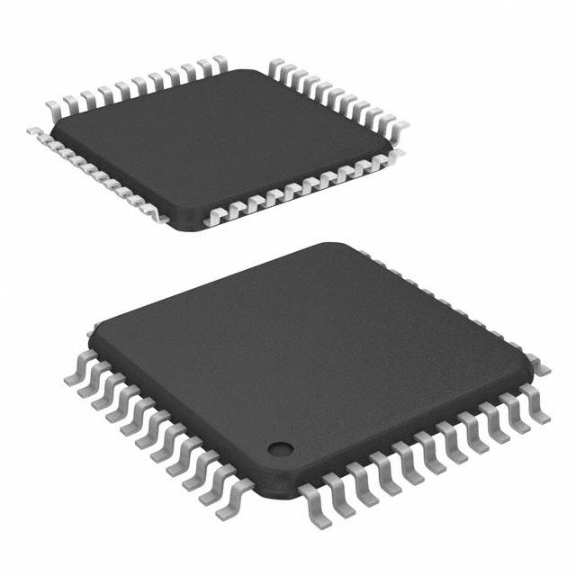
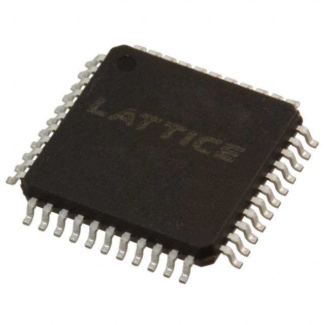
| 描述 | IC CPLD 32MC 5.5NS 44VQFP |
| 产品分类 | |
| I/O数 | 33 |
| 品牌 | Xilinx Inc |
| 数据手册 | |
| 产品图片 |
|
| 产品型号 | XC2C32A-6VQG44C |
| rohs | 无铅 / 符合限制有害物质指令(RoHS)规范要求 |
| 产品系列 | CoolRunner II |
| 产品目录页面 | |
| 供应商器件封装 | 44-VQFP(10x10) |
| 其它名称 | 122-1404 |
| 包装 | 托盘 |
| 可编程类型 | 系统内可编程 |
| 安装类型 | 表面贴装 |
| 宏单元数 | 32 |
| 封装/外壳 | 44-TQFP |
| 工作温度 | 0°C ~ 70°C |
| 延迟时间tpd(1)最大值 | 5.5ns |
| 栅极数 | 750 |
| 标准包装 | 160 |
| 电源电压-内部 | 1.7 V ~ 1.9 V |
| 逻辑元件/块数 | 2 |


- 商务部:美国ITC正式对集成电路等产品启动337调查
- 曝三星4nm工艺存在良率问题 高通将骁龙8 Gen1或转产台积电
- 太阳诱电将投资9.5亿元在常州建新厂生产MLCC 预计2023年完工
- 英特尔发布欧洲新工厂建设计划 深化IDM 2.0 战略
- 台积电先进制程称霸业界 有大客户加持明年业绩稳了
- 达到5530亿美元!SIA预计今年全球半导体销售额将创下新高
- 英特尔拟将自动驾驶子公司Mobileye上市 估值或超500亿美元
- 三星加码芯片和SET,合并消费电子和移动部门,撤换高东真等 CEO
- 三星电子宣布重大人事变动 还合并消费电子和移动部门
- 海关总署:前11个月进口集成电路产品价值2.52万亿元 增长14.8%


PDF Datasheet 数据手册内容提取
0 R XC2C32A CoolRunner-II CPLD DS310 (v2.1) November 6, 2008 Product Specification 0 0 Features Description (cid:129) Optimized for 1.8V systems The CoolRunner™-II 32-macrocell device is designed for - As fast as 3.8ns pin-to-pin logic delays both high performance and low power applications. This - As low as 12 μA quiescent current lends power savings to high-end communication equipment and high speed to battery operated devices. Due to the low (cid:129) Industry’s best 0.18 micron CMOS CPLD power stand-by and dynamic operation, overall system reli- - Optimized architecture for effective logic synthesis ability is improved. - Multi-voltage I/O operation: 1.5V through 3.3V This device consists of two Function Blocks interconnected (cid:129) Available in multiple package options by a low power Advanced Interconnect Matrix (AIM). The - 32-land QFN with 21 user I/Os AIM feeds 40 true and complement inputs to each Function - 44-pin VQFP with 33 user I/Os Block. The Function Blocks consist of a 40 by 56 P-term - 56-ball CP BGA with 33 user I/Os PLA and 16 macrocells which contain numerous configura- - Pb-free available for all packages tion bits that allow for combinational or registered modes of (cid:129) Advanced system features operation. - Fastest in system programming Additionally, these registers can be globally reset or preset · 1.8V ISP using IEEE 1532 (JTAG) interface and configured as a D or T flip-flop or as a D latch. There - IEEE1149.1 JTAG Boundary Scan Test are also multiple clock signals, both global and local product - Optional Schmitt-trigger input (per pin) term types, configured on a per macrocell basis. Output pin - Two separate I/O banks configurations include slew rate limit, bus hold, pull-up, - RealDigital 100% CMOS product term generation open drain, and programmable grounds. A Schmitt trigger - Flexible clocking modes input is available on a per input pin basis. In addition to stor- - Optional DualEDGE triggered registers ing macrocell output states, the macrocell registers can be - Global signal options with macrocell control configured as "direct input" registers to store signals directly · Multiple global clocks with phase selection per from input pins. macrocell · Multiple global output enables Clocking is available on a global or Function Block basis. · Global set/reset Three global clocks are available for all Function Blocks as a - Efficient control term clocks, output enables and synchronous clock source. Macrocell registers can be indi- set/resets for each macrocell and shared across vidually configured to power up to the zero or one state. A function blocks global set/reset control line is also available to asynchro- - Advanced design security nously set or reset selected registers during operation. - Open-drain output option for Wired-OR and LED Additional local clock, synchronous clock-enable, asynchro- drive nous set/reset, and output enable signals can be formed - Optional configurable grounds on unused I/Os using product terms on a per-macrocell or per-Function - Optional bus-hold, 3-state, or weak pullup on Block basis. selected I/O pins The CoolRunner-II 32-macrocell CPLD is I/O compatible - Mixed I/O voltages compatible with 1.5V, 1.8V, with standard LVTTL and LVCMOS18, LVCMOS25, and 2.5V, and 3.3V logic levels LVCMOS33 (see Table1). This device is also 1.5V I/O com- - PLA architecture patible with the use of Schmitt-trigger inputs. · Superior pinout retention Another feature that eases voltage translation is I/O bank- · 100% product term routability across function ing. Two I/O banks are available on the CoolRunner-II32A block macrocell device that permit easy interfacing to 3.3V, 2.5V, - Hot pluggable 1.8V, and 1.5V devices. Refer to the CoolRunner™-II family data sheet for the archi- tecture description. © 2004–2008 Xilinx, Inc. All Xilinx trademarks, registered trademarks, patents, and disclaimers are as listed at http://www.xilinx.com/legal.htm. All other trademarks and registered trademarks are the property of their respective owners. All specifications are subject to change without notice. DS310 (v2.1) November 6, 2008 www.xilinx.com 1 Product Specification
XC2C32A CoolRunner-II CPLD R RealDigital Design Technology LVCMOSstandard is used in 3.3V, 2.5V, and 1.8V applica- tions. CoolRunner-II CPLDs are also 1.5V I/O compatible Xilinx® CoolRunner-II CPLDs are fabricated on a with the use of Schmitt-trigger inputs. 0.18micron process technology which is derived from lead- ing edge FPGA product development. CoolRunner-II Table 1: I/O Standards for XC2C32A CPLDs employ RealDigital, a design technique that makes Board use of CMOS technology in both the fabrication and design IOSTANDARD Output Input Input Termination methodology. RealDigital design technology employs a cas- Attribute V V V Voltage V cade of CMOS gates to implement sum of products instead CCIO CCIO REF T of traditional sense amplifier methodology. Due to this tech- LVTTL 3.3 3.3 N/A N/A nology, Xilinx CoolRunner-II CPLDs achieve both high per- LVCMOS33 3.3 3.3 N/A N/A formance and low power operation. LVCMOS25 2.5 2.5 N/A N/A LVCMOS18 1.8 1.8 N/A N/A Supported I/O Standards LVCMOS15(1) 1.5 1.5 N/A N/A The CoolRunner-II CPLD 32 macrocell features both 1. LVCMOS15 requires Schmitt-trigger inputs. LVCMOS and LVTTL I/O implementations. See Table1 for I/O standard voltages. The LVTTL I/O standard is a general purpose EIA/JEDEC standard for 3.3V applications that use an LVTTL input buffer and Push-Pull output buffer. The 20 15 A) m (C 10 C I 5 0 0 50 100 150 200 250 300 Frequency (MHz) DS091_01_030105 Figure 1: I vs. Frequency CC Table 2: I vs. Frequency (LVCMOS 1.8V T = 25°C)(1) CC A Frequency (MHz) 0 25 50 75 100 150 175 200 225 250 300 Typical I (mA) 0.016 0.87 1.75 2.61 3.44 5.16 5.99 6.81 7.63 8.36 9.93 CC Notes: 1. 16-bit up/down, resettable binary counter (one counter per function block). 2 www.xilinx.com DS310 (v2.1) November 6, 2008 Product Specification
R XC2C32A CoolRunner-II CPLD Absolute Maximum Ratings Symbol Description Value Units V Supply voltage relative to ground –0.5 to 2.0 V CC V Supply voltage for output drivers –0.5 to 4.0 V CCIO V (2) JTAG input voltage limits –0.5 to 4.0 V JTAG V JTAG input supply voltage –0.5 to 4.0 V CCAUX V (1) Input voltage relative to ground –0.5 to 4.0 V IN V (1) Voltage applied to 3-state output –0.5 to 4.0 V TS T (3) Storage Temperature (ambient) –65 to +150 °C STG T Junction Temperature +150 °C J Notes: 1. Maximum DC undershoot below GND must be limited to either 0.5V or 10 mA, whichever is easiest to achieve. During transitions, the device pins might undershoot to –2.0V or overshoot to +4.5V, provided this overshoot or undershoot lasts less than 10ns and with the forcing current being limited to 200 mA. 2. Valid over commercial temperature range. 3. For soldering guidelines and thermal considerations, see the Device Packaging information on the Xilinx website. For Pb free packages, see XAPP427. Recommended Operating Conditions Symbol Parameter Min Max Units V Supply voltage for internal logic Commercial T = 0°C to +70°C 1.7 1.9 V CC A and input buffers Industrial T = –40°C to +85°C 1.7 1.9 V A V Supply voltage for output drivers @ 3.3V operation 3.0 3.6 V CCIO Supply voltage for output drivers @ 2.5V operation 2.3 2.7 V Supply voltage for output drivers @ 1.8V operation 1.7 1.9 V Supply voltage for output drivers @ 1.5V operation 1.4 1.6 V V JTAG programming pins 1.7 3.6 V CCAUX DC Electrical Characteristics Over Recommended Operating Conditions Symbol Parameter Test Conditions Typical Max. Units I Standby current Commercial V = 1.9V, V = 3.6V 22 90 μA CCSB CC CCIO I Standby current Industrial V = 1.9V, V = 3.6V 38 150 μA CCSB CC CCIO I (1) Dynamic current f = 1 MHz - 0.25 mA CC f = 50 MHz - 2.5 mA C JTAG input capacitance f = 1 MHz - 10 pF JTAG C Global clock input capacitance f = 1 MHz - 12 pF CLK C I/O capacitance f = 1 MHz - 10 pF IO I (2) Input leakage current V = 0V or V to 3.9V - +/-1 μA IL IN CCIO I (2) I/O High-Z leakage V = 0V or V to 3.9V - +/-1 μA IH IN CCIO Notes: 1. 16-bit up/down resettable binary counter (one per Function Block) tested at V = V = 1.9V. CC CCIO 2. See Quality and Reliability section of the CoolRunner-II family data sheet. DS310 (v2.1) November 6, 2008 www.xilinx.com 3 Product Specification
XC2C32A CoolRunner-II CPLD R LVCMOS 3.3V and LVTTL 3.3V DC Voltage Specifications Symbol Parameter Test Conditions Min. Max. Units V Input source voltage 3.0 3.6 V CCIO V High level input voltage 2 3.9 V IH V Low level input voltage –0.3 0.8 V IL V High level output voltage I = –8 mA, V = 3V V – 0.4V - V OH OH CCIO CCIO I = –0.1 mA, V = 3V V – 0.2V - V OH CCIO CCIO V Low level output voltage I = 8 mA, V = 3V - 0.4 V OL OL CCIO I = 0.1 mA, V = 3V - 0.2 V OL CCIO LVCMOS 2.5V DC Voltage Specifications Symbol Parameter Test Conditions Min. Max. Units V Input source voltage 2.3 2.7 V CCIO V High level input voltage 1.7 V + 0.3(1) V IH CCIO V Low level input voltage –0.3 0.7 V IL V High level output voltage I = –8 mA, V = 2.3V V – 0.4V - V OH OH CCIO CCIO I = –0.1 mA, V = 2.3V V – 0.2V - V OH CCIO CCIO V Low level output voltage I = 8 mA, V = 2.3V - 0.4 V OL OL CCIO I = 0.1mA, V = 2.3V - 0.2 V OL CCIO 1. The V Max value represents the JEDEC specification for LVCMOS25. The CoolRunner-II CPLD input buffer can tolerate up to 3.9V IH without physical damage. LVCMOS 1.8V DC Voltage Specifications Symbol Parameter(1) Test Conditions Min. Max. Units V Input source voltage 1.7 1.9 V CCIO V High level input voltage 0.65 x V V + 0.3(1) V IH CCIO CCIO V Low level input voltage –0.3 0.35 x V V IL CCIO V High level output voltage I = –8 mA, V = 1.7V V – 0.45 - V OH OH CCIO CCIO I = –0.1 mA, V = 1.7V V – 0.2 - V OH CCIO CCIO V Low level output voltage I = 8 mA, V = 1.7V - 0.45 V OL OL CCIO I = 0.1 mA, V = 1.7V - 0.2 V OL CCIO 1. The V Max value represents the JEDEC specification for LVCMOS18. The CoolRunner-II CPLD input buffer can tolerate up to 3.9V IH without physical damage. LVCMOS 1.5V DC Voltage Specifications Symbol Parameter Test Conditions Min. Max. Units V Input source voltage 1.4 1.6 V CCIO V Input hysteresis threshold voltage 0.5 x V 0.8 x V V T+ CCIO CCIO V 0.2 x V 0.5 x V V T- CCIO CCIO V High level output voltage I = –8 mA, V = 1.4V V – 0.45 - V OH OH CCIO CCIO I = –0.1 mA, V = 1.4V V – 0.2 - V OH CCIO CCIO V Low level output voltage I = 8 mA, V = 1.4V - 0.4 V OL OL CCIO I = 0.1 mA, V = 1.4V - 0.2 V OL CCIO Notes: 1. Hysteresis used on 1.5V inputs. 4 www.xilinx.com DS310 (v2.1) November 6, 2008 Product Specification
R XC2C32A CoolRunner-II CPLD Schmitt Trigger Input DC Voltage Specifications Symbol Parameter Test Conditions Min. Max. Units V Input source voltage 1.4 3.9 V CCIO V Input hysteresis threshold voltage 0.5 x V 0.8 x V V T+ CCIO CCIO V 0.2 x V 0.5 x V V T- CCIO CCIO AC Electrical Characteristics Over Recommended Operating Conditions -4 -6 Symbol Parameter Min. Max. Min. Max. Units T Propagation delay single p-term - 3.8 - 5.5 ns PD1 T Propagation delay OR array - 4.0 - 6.0 ns PD2 T Direct input register clock setup time 1.7 - 2.2 - ns SUD T Setup time fast (single p-term) 1.9 - 2.6 - ns SU1 T Setup time (OR array) 2.1 - 3.1 - ns SU2 T Direct input register hold time 0.0 - 0.0 - ns HD T P-term hold time 0.0 - 0.0 - ns H T Clock to output - 3.7 - 4.7 ns CO F (1) Internal toggle rate - 500 - 300 MHz TOGGLE F (2) Maximum system frequency - 323 - 200 MHz SYSTEM1 F (2) Maximum system frequency - 303 - 182 MHz SYSTEM2 F (3) Maximum external frequency - 179 - 137 MHz EXT1 F (3) Maximum external frequency - 172 - 128 MHz EXT2 T Direct input register p-term clock setup time 0.4 - 0.9 - ns PSUD T P-term clock setup time (single p-term) 0.6 - 1.3 - ns PSU1 T P-term clock setup time (OR array) 0.8 - 1.8 - ns PSU2 T Direct input register p-term clock hold time 1.5 - 1.6 - ns PHD T P-term clock hold 1.3 - 1.2 - ns PH T P-term clock to output - 5.0 - 6.0 ns PCO T /T Global OE to output enable/disable - 4.7 - 5.5 ns OE OD T /T P-term OE to output enable/disable - 6.2 - 6.7 ns POE POD T /T Macrocell driven OE to output enable/disable - 6.2 - 6.9 ns MOE MOD T P-term set/reset to output valid - 5.5 - 6.8 ns PAO T Global set/reset to output valid - 4.5 - 5.5 ns AO T Register clock enable setup time 2.0 - 3.0 - ns SUEC T Register clock enable hold time 0.0 - 0.0 - ns HEC T Global clock pulse width High or Low 1.4 - 2.2 - ns CW T P-term pulse width High or Low 4.0 - 6.0 - ns PCW T Asynchronous preset/reset pulse width (High or Low) 4.0 - 6.0 - ns APRPW T (4) Configuration time - 50 - 50 μs CONFIG Notes: 1. F is the maximum clock frequency to which a T-Flip Flop can reliably toggle (see the CoolRunner-II family data sheet). TOGGLE 2. F (1/T ) is the internal operating frequency for a device fully populated with one 16-bit counter through one p-term per SYSTEM1 CYCLE macrocell while F is through the OR array. SYSTEM2 3. F (1/T +T ) is the maximum external frequency using one p-term while F is through the OR array. EXT1 SU1 CO EXT2 4. Typical configuration current during T is 500 μA. CONFIG DS310 (v2.1) November 6, 2008 www.xilinx.com 5 Product Specification
XC2C32A CoolRunner-II CPLD R Internal Timing Parameters -4 -6 Symbol Parameter(1) Min. Max. Min. Max. Units Buffer Delays T Input buffer delay - 1.3 - 1.7 ns IN T Direct register input delay - 1.5 - 2.4 ns DIN T Global Clock buffer delay - 1.3 - 2.0 ns GCK T Global set/reset buffer delay - 1.6 - 2.0 ns GSR T Global 3-state buffer delay - 1.1 - 2.1 ns GTS T Output buffer delay - 1.8 - 2.0 ns OUT T Output buffer enable/disable delay - 2.9 - 3.4 ns EN P-term Delays T Control term delay - 1.3 - 1.6 ns CT T Single p-term delay adder - 0.4 - 1.1 ns LOGI1 T Multiple p-term delay adder - 0.2 - 0.5 ns LOGI2 Macrocell Delay T Input to output valid - 0.3 - 0.7 ns PDI T Setup before clock (transparent latch) - 1.5 - 2.5 ns LDI T Setup before clock 1.5 - 1.8 - ns SUI T Hold after clock 0.0 - 0.0 - ns HI T Enable clock setup time 0.7 - 1.7 - ns ECSU T Enable clock hold time 0.0 - 0.0 - ns ECHO T Clock to output valid - 0.6 - 0.7 ns COI T Set/reset to output valid - 1.1 - 1.5 ns AOI Feedback Delays T Feedback delay - 0.6 - 1.4 ns F T Macrocell to global OE delay - 0.7 - 0.8 ns OEM I/O Standard Time Adder Delays 1.5V CMOS T Hysteresis input adder - 3.0 - 4.0 ns HYS15 T Output adder - 0.8 - 1.0 ns OUT15 T Output slew rate adder - 4.0 - 5.0 ns SLEW15 I/O Standard Time Adder Delays 1.8V CMOS T Hysteresis input adder - 3.0 - 4.0 ns HYS18 T Output adder - 0.0 - 0.0 ns OUT18 T Output slew rate adder - 4.0 - 5.0 ns SLEW 6 www.xilinx.com DS310 (v2.1) November 6, 2008 Product Specification
R XC2C32A CoolRunner-II CPLD Internal Timing Parameters (Continued) -4 -6 Symbol Parameter(1) Min. Max. Min. Max. Units I/O Standard Time Adder Delays 2.5V CMOS T Standard input adder - 0.5 - 0.6 ns IN25 T Hysteresis input adder - 3.0 - 4.0 ns HYS25 T Output adder - 0.6 - 0.7 ns OUT25 T Output slew rate adder - 4.0 - 5.0 ns SLEW25 I/O Standard Time Adder Delays 3.3V CMOS/TTL T Standard input adder - 0.5 - 0.6 ns IN33 T Hysteresis input adder - 3.0 - 4.0 ns HYS33 T Output adder - 1.0 - 1.2 ns OUT33 T Output slew rate adder - 4.0 - 5.0 ns SLEW33 Notes: 1. 1.5 ns input pin signal rise/fall. Switching Characteristics AC Test Circuit VCC = VCCIO = 1.8V @ 25oC VCC 5.5 R1 5.0 Device Test Point Under Test 4.5 R2 CL s) n (2 4.0 D TP Output Type R1 R2 CL LVTTL33 268Ω 235Ω 35 pF 3.5 LVCMOS33 275Ω 275Ω 35 pF LVCMOS25 188Ω 188Ω 35pF 3.0 LVCMOS18 112.5Ω 112.5Ω 35pF 1 2 4 8 16 LVCMOS15 150Ω 150Ω 35pF Number of Outputs Switching CL includes test fixtures and probe capacitance. 1.5 nsec maximum rise/fall times on inputs. DS091_02_112002 Figure 2: Derating Curve for T DS310_03_102108 PD Figure 3: AC Load Circuit DS310 (v2.1) November 6, 2008 www.xilinx.com 7 Product Specification
XC2C32A CoolRunner-II CPLD R Typical I/O Output Curves 3.3V 60 50 A) m ent 40 2.5V urr 1.8V C put 30 Iol ut O O ( I 20 1.5V 10 0 0 .5 1.0 1.5 2.0 2.5 3.0 3.5 VO (Output Volts) XC32_VoIo_all_0403 Figure 4: Typical I/V Curve for XC2C32A Pin Descriptions Function Block Macrocell QFG32 PC44(1) VQ44 CP56 I/O Bank 1 1 44 38 F1 Bank 2 1 2 43 37 E3 Bank 2 1 3 42 36 E1 Bank 2 1(GTS1) 4 3 40 34 D1 Bank 2 1(GTS0) 5 2 39 33 C1 Bank 2 1(GTS3) 6 1 38 32 A3 Bank 2 1(GTS2) 7 32 37 31 A2 Bank 2 1(GSR) 8 31 36 30 B1 Bank 2 1 9 30 35 29 A1 Bank 2 1 10 29 34 28 C4 Bank 2 1 11 28 33 27 C5 Bank 2 1 12 24 29 23 C8 Bank 2 1 13 28 22 A10 Bank 2 1 14 23 27 21 B10 Bank 2 1 15 26 20 C10 Bank 2 1 16 25 19 E8 Bank 2 2 1 5 1 39 G1 Bank 1 2 2 2 40 F3 Bank 1 2 3 3 41 H1 Bank 1 2 4 4 42 G3 Bank 1 2(GCK0) 5 6 5 43 J1 Bank 1 2(GCK1) 6 7 6 44 K1 Bank 1 2(GCK2) 7 8 7 1 K2 Bank 1 8 www.xilinx.com DS310 (v2.1) November 6, 2008 Product Specification
R XC2C32A CoolRunner-II CPLD Pin Descriptions (Continued) Function Block Macrocell QFG32 PC44(1) VQ44 CP56 I/O Bank 2 8 9 8 2 K3 Bank 1 2 9 10 9 3 H3 Bank 1 2 10 11 5 K5 Bank 1 2 11 12 6 H5 Bank 1 2 12 13 14 8 H8 Bank 1 2 13 17 18 12 K8 Bank 1 2 14 18 19 13 H10 Bank 1 2 15 19 20 14 G10 Bank 1 2 16 22 16 F10 Bank 1 Notes: 1. This is an obsolete package type. It remains here for legacy support only. 2. GTS = global output enable, GSR = global set reset, GCK = global clock. 3. GTS, GSR, and GCK pins can also be used for general purpose I/O. XC2C32A Global, JTAG, Power/Ground, and No Connect Pins Pin Type QFG32 PC44(1)(2) VQ44(2) CP56(2) TCK 16 17 11 K10 TDI 14 15 9 J10 TDO 25 30 24 A6 TMS 15 16 10 K9 Input Only 22 (bank 2) 24 (bank 2) 18 (bank 2) D10 (bank 2) V (JTAG supply voltage) 4 41 35 D3 CCAUX Power internal (V ) 20 21 15 G8 CC Power bank 1 I/O (V ) 12 13 7 H6 CCIO1 Power bank 2 I/O (V ) 27 32 26 C6 CCIO2 Ground 11, 21, 26 10,23,31 4,17,25 H4, F8, C7 No connects - - K4, K6, K7, H7, E10, A7, A9, D8, A5, A8, A4, C3 Total user I/O (includes dual function pins) 21 33 33 33 Notes: 1. This is an obsolete package type. It remains here for legacy support only. 2. All packages pin compatible with larger macrocell densities. DS310 (v2.1) November 6, 2008 www.xilinx.com 9 Product Specification
XC2C32A CoolRunner-II CPLD R Ordering Information Pin/Ball θ θ Package Body Comm. (C) JA JC Part Number Spacing (°C/Watt) (°C/Watt) Package Type Dimensions I/O Ind. (I)(1) XC2C32A-4QFG32C 0.5mm 35.5 24.0 Quad Flat No Lead; Pb-free 5mm x 5mm 21 C XC2C32A-6QFG32C 0.5mm 35.5 24.0 Quad Flat No Lead; Pb-free 5mm x 5mm 21 C XC2C32A-4VQ44C 0.8mm 47.7 8.2 Very Thin Quad Flat Pack 10mm x 10mm 33 C XC2C32A-6VQ44C 0.8mm 47.7 8.2 Very Thin Quad Flat Pack 10mm x 10mm 33 C XC2C32A-4CP56C 0.5mm 66.0 14.9 Chip Scale Package 6mm x 6mm 33 C XC2C32A-6CP56C 0.5mm 66.0 14.9 Chip Scale Package 6mm x 6mm 33 C XC2C32A-4VQG44C 0.8mm 47.7 8.2 Very Thin Quad Flat Pack; Pb-free 10mm x 10mm 33 C XC2C32A-6VQG44C 0.8mm 47.7 8.2 Very Thin Quad Flat Pack; Pb-free 10mm x 10mm 33 C XC2C32A-4CPG56C 0.5mm 66.0 14.9 Chip Scale Package; Pb-free 6mm x 6mm 33 C XC2C32A-6CPG56C 0.5mm 66.0 14.9 Chip Scale Package; Pb-free 6mm x 6mm 33 C XC2C32A-6QFG32I 0.5mm 35.5 24.0 Quad Flat No Lead; Pb-free 5mm x 5mm 21 I XC2C32A-6VQ44I 0.8mm 47.7 8.2 Very Thin Quad Flat Pack 10mm x 10mm 33 I XC2C32A-6CP56I 0.5mm 66.0 14.9 Chip Scale Package 6mm x 6mm 33 I XC2C32A-6VQG44I 0.8mm 47.7 8.2 Very Thin Quad Flat Pack; Pb-free 10mm x 10mm 33 I XC2C32A-6CPG56I 0.5mm 66.0 14.9 Chip Scale Package; Pb-free 6mm x 6mm 33 I Notes: 1. C = Commercial (TA = 0°C to +70°C); I = Industrial (TA = –40°C to +85°C) Standard Example: X C 2 C 1 28 - 4 TQ 144 C Pb-Free Example: X C 2 C 1 28 -4 TQ G 144 C Device Device Speed Grade Speed Grade Package Type Package Type Number of Pins Pb-Free Temperature Range Number of Pins Temperature Range Device Part Marking R Device Type XC2Cxxx Package TQ144 This line not related to device part number Speed 7C Operating Range Part marking for non-chip scale package DS310_05_102108 Figure 5: Sample Package with Part Marking Note: Due to the small size of chip scale and quad flat no lead packages, the complete ordering part number cannot be included on the package marking. Part marking on chip scale and quad flat no lead packages by line are: (cid:129) Line 1 = X (Xilinx logo) then truncated part number (cid:129) Line 4 = Package code, speed, operating temperature, (cid:129) Line 2 = Not related to device part number three digits not related to device part number. Package codes: C3 = CP56, C4 = CPG56, Q1 = QFG32. (cid:129) Line 3 = Not related to device part number 10 www.xilinx.com DS310 (v2.1) November 6, 2008 Product Specification
R XC2C32A CoolRunner-II CPLD 2 I/O(1)I/O(3)I/OI/OI/OVccioGndTDO I/O(2) I/O(2) I/OI/OI/OI/OI/OI/OI/OVAUXI/O(1) 43210987654 I/O(1) 1323130292827262524 I/O I/O(2) 1 4444433333333 I/O(1) I/O(1) 2 I/O I/O 2 32 I/O(1) 23 I/O 3 31 I/O(1) I/O(1) 3 22 Input GND 4 30 I/O(3) VAUX 4 QFG32 21 Gnd II//OO 56 ToVpQ V4i4ew 2298 II//OO Top View I/O 5 20 Vcc VCCIO1 7 27 I/O I/O(2) 6 19 I/O TI/DOI 89 2265 VGCNCDIO2 I/O(2) 7 18 I/O TMS 10 24 TDO I/O(2) 8 012345617 I/O TCK 11121314151617181920212223 I/O 91111111 OOndccio1ODIMSCK I/OI/OI/OVCCI/OGND II/OI/OI/OI/O I/I/GVI/TTT (1) - Global Output Enable (1) - Global Output Enable (2) - Global Clock (2) - Global Clock (3) - Global Set/Reset (3) - Global Set/Reset Figure 6: QFG32 Package Figure 7: VQ44 Package O(2) O(2) OOOOOOO AUXO(1) I/I/I/I/I/I/I/I/I/VI/ 65432143210 I/O(2) 7 4444439 I/O(1) I/O 8 38 I/O(1) I/O 9 37 I/O(1) GND 10 36 I/O(3) PC44 I/O 11 35 I/O I/O 12 Top View 34 I/O VCCIO1 13 33 I/O I/O 14 32 VCCIO2 TDI 15 31 Gnd TMS 16 30 TDO TCK 17 29 I/O 89012345678 11222222222 OOO CODIOOOO I/I/I/VCI/GN I/I/I/I/ (1) - Global Output Enable (2) - Global Clock (3) - Global Set/Reset Figure 8: PC44 Package DS310 (v2.1) November 6, 2008 www.xilinx.com 11 Product Specification
XC2C32A CoolRunner-II CPLD R 0 1 2 3 4 5 6 7 8 9 1 K I/O(2) I/O(2) I/O NC I/O NC NC I/O TMS TCK J I/O(2) TDI H I/O I/O GND I/O VCC NC I/O I/O IO1 G I/O I/O V I/O CC F I/O I/O CP56 GND I/O Bottom View E I/O I/O I/O NC D I/O(1) V NC I AUX C I/O(1) NC I/O I/O VCC GND I/O I/O IO2 B I/O(3) I/O A I/O I/O(1) I/O(1) NC NC TDO NC NC NC I/O (1) - Global Output Enable (2) - Global Clock (3) - Global Set/Reset Figure 9: CP56 Package Warranty Disclaimer THESE PRODUCTS ARE SUBJECT TO THE TERMS OF THE XILINX LIMITED WARRANTY WHICH CAN BE VIEWED AT http://www.xilinx.com/warranty.htm. THIS LIMITED WARRANTY DOES NOT EXTEND TO ANY USE OF THE PRODUCTS IN AN APPLICATION OR ENVIRONMENT THAT IS NOT WITHIN THE SPECIFICATIONS STATED ON THE THEN-CURRENT XILINX DATA SHEET FOR THE PRODUCTS. PRODUCTS ARE NOT DESIGNED TO BE FAIL-SAFE AND ARE NOT WARRANTED FOR USE IN APPLICATIONS THAT POSE A RISK OF PHYSICAL HARM OR LOSS OF LIFE. USE OF PRODUCTS IN SUCH APPLICATIONS IS FULLY AT THE RISK OF CUSTOMER SUBJECT TO APPLICABLE LAWS AND REGULATIONS. 12 www.xilinx.com DS310 (v2.1) November 6, 2008 Product Specification
R XC2C32A CoolRunner-II CPLD Additional Information Additional information is available for the following CoolRunner-II topics: (cid:129) XAPP784: Bulletproof CPLD Design Practices To access these and all application notes with their associ- (cid:129) XAPP375: Timing Model ated reference designs, click the following links and scroll down the page until you find the document you want: (cid:129) XAPP376: Logic Engine (cid:129) XAPP378: Advanced Features CoolRunner-II CPLD Data Sheets and Application Notes (cid:129) XAPP382: I/O Characteristics Device Packages (cid:129) XAPP389: Powering CoolRunner-II (cid:129) XAPP399: Assigning VREF Pins Revision History The following table shows the revision history for this document. Date Version Revision 6/15/04 1.0 Initial Xilinx release. 8/30/04 1.1 Pb-free documentation 10/01/04 1.2 Add Asynchronous Preset/Reset Pulse Width specification to AC Electrical Characteristics. 11/08/04 1.3 Product Release. No changes to documentation. 11/22/04 1.4 Changes to output enable/disable specifications; changes to I . CCSB 02/17/05 1.5 Changes to f , t , and t TOGGLE SLEW25 SLEW33 03/07/05 1.6 Improvement of pin-to-pin logic delay, page 1. Modifications to Table 1, IOSTANDARDs. 06/28/05 1.7 Move to Product Specification. Change to T , T , T , and T . IN25 OUT25 IN33 OUT33 03/20/06 1.8 Add Warranty Disclaimer. Add note to Pin Descriptions that GCK, GSR, and GTS pins can also be used for general purpose I/O. 02/15/07 1.9 Change to V specification for 2.5V and 1.8V LVCMOS. Change to T for -4 speed IH OEM grade. 03/08/07 2.0 Fixed typo in note for V for LVCMOS18; removed note for V for LVCMOS33. IL IL 11/06/08 2.1 Added note to Pin Description tables to indicate the PC44 packages are obsolete. Removed part numbers for devices in PC44 packages from ordering information. See Product Discontinuation Notice xcn07022.pdf. DS310 (v2.1) November 6, 2008 www.xilinx.com 13 Product Specification
XC2C32A CoolRunner-II CPLD R 14 www.xilinx.com DS310 (v2.1) November 6, 2008 Product Specification