ICGOO在线商城 > 射频/IF 和 RFID > RF 定向耦合器 > XC1400P-03S
 Datasheet下载
- 型号: XC1400P-03S
- 制造商: Anaren Microwave
- 库位|库存: xxxx|xxxx
- 要求:
| 数量阶梯 | 香港交货 | 国内含税 |
| +xxxx | $xxxx | ¥xxxx |
查看当月历史价格
查看今年历史价格
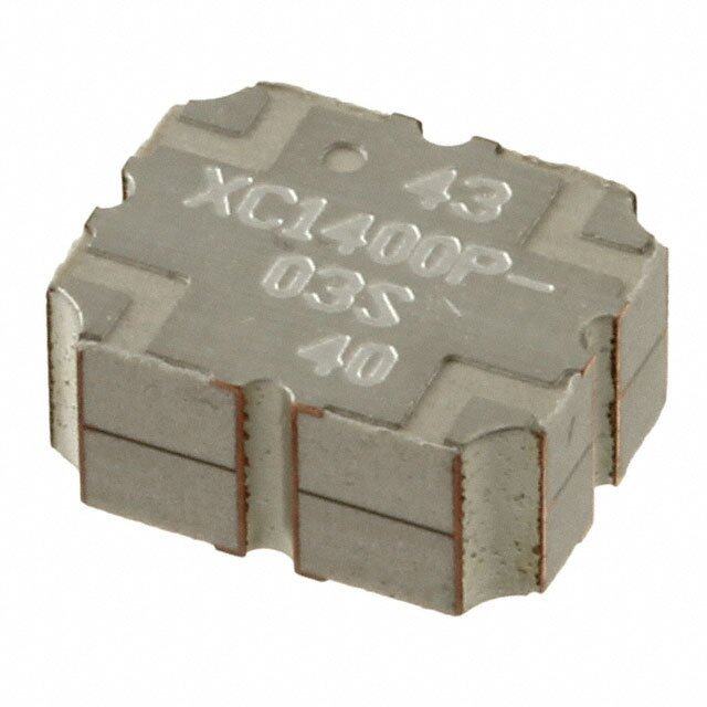
XC1400P-03S产品简介:
ICGOO电子元器件商城为您提供XC1400P-03S由Anaren Microwave设计生产,在icgoo商城现货销售,并且可以通过原厂、代理商等渠道进行代购。 XC1400P-03S价格参考¥13.92-¥27.81。Anaren MicrowaveXC1400P-03S封装/规格:RF 定向耦合器, RF Directional Coupler General Purpose 1.2GHz ~ 1.6GHz 40W 4-SMD, No Lead。您可以下载XC1400P-03S参考资料、Datasheet数据手册功能说明书,资料中有XC1400P-03S 详细功能的应用电路图电压和使用方法及教程。
Anaren品牌的RF定向耦合器型号XC1400P-03S主要应用于射频(RF)和微波通信领域,其具体应用场景包括:

1. 信号监测与测量:该耦合器可用于实时监测射频信号的功率、相位和质量。例如,在基站或无线通信设备中,通过提取一小部分主信号进行分析,确保系统正常运行。

2. 功率分配与合成:在多通道射频系统中,XC1400P-03S可以用于分配输入信号或将多个信号合成一个输出信号,同时保持信号的稳定性和低插入损耗。

3. 雷达系统:在雷达应用中,此型号的耦合器可用于发射机和接收机之间的信号分离,确保发射信号不会干扰接收信号,同时支持回波信号的精确检测。

4. 无线通信设备:适用于蜂窝网络、Wi-Fi、蓝牙等无线通信设备中的信号处理环节,帮助优化信号传输效率并减少干扰。

5. 测试与测量设备:在实验室环境中,XC1400P-03S可集成到矢量网络分析仪(VNA)、频谱分析仪等设备中,用于评估射频组件的性能。

6. 卫星通信:在卫星地面站或卫星终端中,该耦合器可用于信号放大链路中的功率监控和保护,以防止过载或损坏敏感元件。

7. 医疗设备:在需要高频信号处理的医疗设备(如MRI或超声波成像系统)中,XC1400P-03S可提供高精度的信号耦合功能。

8. 工业自动化:在工业物联网(IIoT)中,该耦合器可用于无线传感器网络中的信号增强和远程监控。

总之,XC1400P-03S凭借其宽频带、高隔离度和低插入损耗的特点,广泛适用于各种射频和微波系统的信号处理需求。
| 参数 | 数值 |
| 产品目录 | |
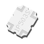
| 描述 | HYBRID COUPLER 3DB 90DEG |
| 产品分类 | |
| 品牌 | Anaren |
| 数据手册 | |
| 产品图片 |
|
| 产品型号 | XC1400P-03S |
| rohs | 无铅 / 符合限制有害物质指令(RoHS)规范要求 |
| 产品系列 | * |
| 供应商器件封装 | SMD |
| 其它名称 | 1173-1146-6 |
| 功率-最大值 | * |
| 包装 | Digi-Reel® |
| 回波损耗 | * |
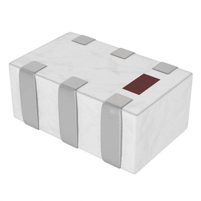
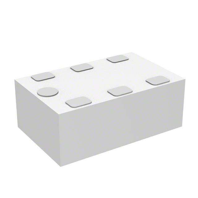
| 封装/外壳 | 4-SMD,无引线 |
| 应用 | * |
| 插入损耗 | * |
| 标准包装 | 1 |
| 耦合器类型 | * |
| 耦合系数 | * |
| 隔离 | * |
| 频率 | * |


- 商务部:美国ITC正式对集成电路等产品启动337调查
- 曝三星4nm工艺存在良率问题 高通将骁龙8 Gen1或转产台积电
- 太阳诱电将投资9.5亿元在常州建新厂生产MLCC 预计2023年完工
- 英特尔发布欧洲新工厂建设计划 深化IDM 2.0 战略
- 台积电先进制程称霸业界 有大客户加持明年业绩稳了
- 达到5530亿美元!SIA预计今年全球半导体销售额将创下新高
- 英特尔拟将自动驾驶子公司Mobileye上市 估值或超500亿美元
- 三星加码芯片和SET,合并消费电子和移动部门,撤换高东真等 CEO
- 三星电子宣布重大人事变动 还合并消费电子和移动部门
- 海关总署:前11个月进口集成电路产品价值2.52万亿元 增长14.8%
PDF Datasheet 数据手册内容提取
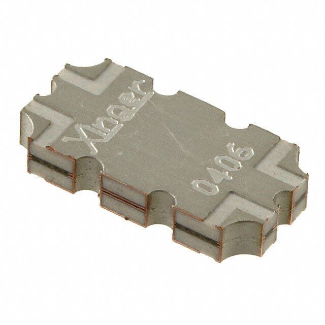
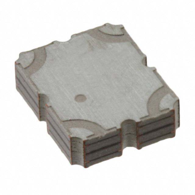
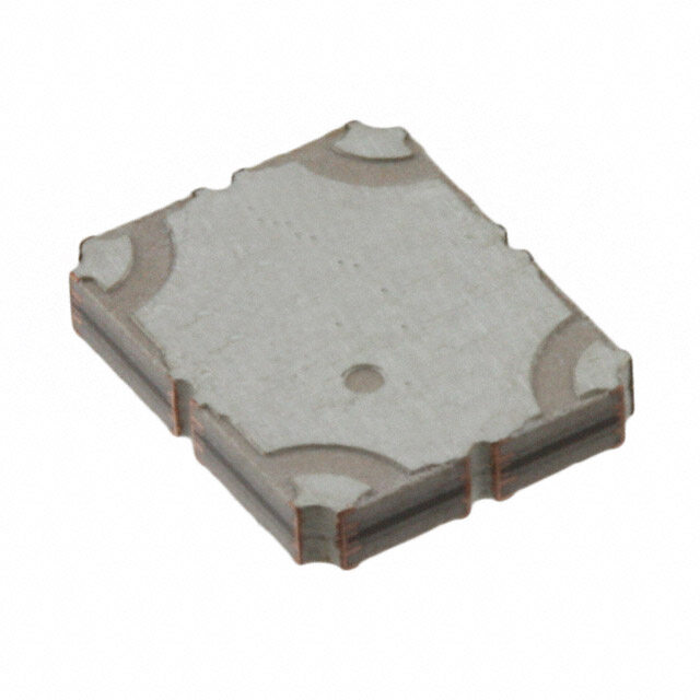
Model XC1400P-03S Rev C Hybrid Coupler 3 dB, 90° Description The XC1400P-03S is a low profile, high performance 3dB hybrid coupler in a new easy to use, manufacturing friendly surface mount package. It is designed for GPS band applications. The XC1400P-03S is designed particularly for balanced power and low noise amplifiers, plus signal distribution and other applications where low insertion loss and tight amplitude and phase balance is required. It can be used in high power applications up to 40 Watts. Parts have been subjected to rigorous qualification testing and they are manufactured using materials with coefficients of thermal expansion (CTE) compatible with common substrates such as FR4, G-10, RF-35, and RO4350. Produced with 6 of 6 RoHS compliant tin immersion. Electrical Specifications ** Features: Insertion Amplitude Frequency Isolation VSWR • 1200 – 1600 MHz Loss Balance • GPS MHz dB Min dB Max Max : 1 dB Max • High Power 1200-1600 23 0.32 1.20 +/-0.30 • Very Low Loss 1215-1240 23 0.23 1.17 +/-0.30 • Tight Amplitude Balance 1563-1588 23 0.32 1.20 +/-0.30 • High Isolation Operating • Production Friendly Phase Power ΘJC Temp. • Tape and Reel • Lead-Free Degrees Avg. CW Watts ºC/Watt ºC • Reliable, FIT=0.49 90 ± 4.0 30 57 -55 to +85 90 ± 3.0 40 57 -55 to +85 90 ± 4.0 30 57 -55 to +85 **Specification based on performance of unit properly installed on Anaren Test Board 54147-0001 with small signal appli ed. Specifications subject to change without notice. Refer to parameter definitions for details. Top View (Near-side) Side View Bottom View (Far-side) .107±.021 4x .020±.004 .250± .010 [2.72±0.54] [0.51±0.10] [6.35±0.25] PIN 1 PIN 2 PIN 2 GND PIN 1 4x .020±.004 [0.51±0.10] ORIENTATION MARKER DENOTES XC1400P- .200 ±.010 .120±.010 PIN 1 03S [5.08±0.25] [3.05±0.25] 4x .034±.004SQ [0.86±0.10] GND PIN 3 PIN 4 DENOTES PIN 3 .170±.010 PIN 4 ARRAY NUMBER [4.32±0.25] Dimensions are in Inches [Millimeters] Tolerances are Non-Cumulative XC1400P-03S Mechanical Outline Rev C Available on Tape USA/Canada: (315) 432-8909 and Reel for Pick and Toll Free: (800) 411-6596 Place Manufacturing. Europe: +44 2392-232392
Model XC1400P-03S Rev C Hybrid Coupler Pin Configuration The XC1400P-03S has an orientation marker to denote Pin 1. Once port one has been identified the other ports are known automatically. Please see the chart below for clarification: Configuration Pin 1 Pin 2 Pin 3 Pin 4 Splitter Input Isolated -3dB ∠θ−90 -3dB ∠θ Splitter Isolated Input -3dB ∠θ -3dB ∠θ−90 Splitter -3dB ∠θ−90 -3dB ∠θ Input Isolated Splitter -3dB ∠θ -3dB ∠θ−90 Isolated Input *Combiner A∠θ−90 A ∠θ Isolated Output *Combiner A∠θ A ∠θ−90 Output Isolated *Combiner Isolated Output A∠θ−90 A ∠θ *Combiner Output Isolated A∠θ A ∠θ−90 *Note: “A” is the amplitude of the applied signals. When two quadrature signals with equal amplitudes are applied to the coupler as described in the table, they will combine at the output port. If the amplitudes are not equal, some of the applied energy will be directed to the isolated port. USA/Canada: (315) 432-8909 Available on Tape and Toll Free: (800) 411-6596 Reel for Pick and Place Europe: +44 2392-232392 Manufacturing.
Model XC1400P-03S Rev C Insertion Loss and Power Derating Curves Typical Insertion Loss Derating Curve for XC1400P-03 Power Derating Curve for XC1400P-03 -0.05 70 typical insertion loss(f=1240Mhz) power handling (f=1240MHz) typical insertion loss(f=1588Mhz) power handling (f=1588MHz) typical insertion loss(f=1600Mhz) power handling (f=1600MHz) -0.1 60 -0.15 50 B) oss (d -0.2 Watts) 40 nsertion L -0.25 Power ( 30 I -0.3 20 -0.35 10 -0.4 0 -50 0 50 100 150 200 250 300 0 25 50 75 100 125 150 175 200 225 Temperature of the Part ( °C) Base Plate Temperature (°C) Insertion Loss Derating: Power Derating: The insertion loss, at a given frequency, of a group of The power handling and corresponding power derating couplers is measured at 25°C and then averaged. The plots are a function of the thermal resistance, mounting measurements are performed under small signal surface temperature (base plate temperature), conditions (i.e. using a Vector Network Analyzer). The maximum continuous operating temperature of the process is repeated at -55°C and 85°C. Based on coupler, and the thermal insertion loss. The thermal copper as well as dielectric losses, the insertion loss is insertion loss is defined in the Power Handling section of computed from -55°C to 300°C. the data sheet. As the mounting interface temperature approaches the maximum continuous operating temperature, the power handling decreases to zero. Available on Tape USA/Canada: (315) 432-8909 and Reel for Pick and Toll Free: (800) 411-6596 Place Manufacturing. Europe: +44 2392-232392
Model XC1400P-03S Rev C Typical Performance (-55°C, 25°C and 85°C): 1200-1600 MHz Return Loss for XC1400P-03(Feeding Port1) Return Loss for XC1400P-03(Feeding Port2) 0 0 -55 °C -55 °C 25 °C 25 °C 85 °C 85 °C -10 -10 -20 -20 B) B) d d s ( s ( os -30 os -30 L L n n ur ur Ret Ret -40 -40 -50 -50 -60 -60 1200 1250 1300 1350 1400 1450 1500 1550 1600 1200 1250 1300 1350 1400 1450 1500 1550 1600 Frequency (MHz) Frequency (MHz) Return Loss for XC1400P-03(Feeding Port3) Return Loss for XC1400P-03(Feeding Port4) 0 0 -55 °C -55 °C 25 °C 25 °C 85 °C 85 °C -10 -10 -20 -20 B) B) d d s ( s ( os -30 os -30 L L n n ur ur Ret Ret -40 -40 -50 -50 -60 -60 1200 1250 1300 1350 1400 1450 1500 1550 1600 1200 1250 1300 1350 1400 1450 1500 1550 1600 Frequency (MHz) Frequency (MHz) USA/Canada: (315) 432-8909 Available on Tape and Toll Free: (800) 411-6596 Reel for Pick and Place Europe: +44 2392-232392 Manufacturing.
Model XC1400P-03S Rev C Typical Performance (-55°C, 25°C and 85°C): 1200-1600 MHz Coupling for XC1400P-03(Feeding Port1) Insertion Loss for XC1400P-03(Feeding Port1) -2.8 0 -55 °C -55 °C 25 °C 25 °C 85 °C 85 °C -2.9 -0.05 -3 B) -0.1 Coupling (dB) -3.1 ertion Loss (d ns -0.15 I -3.2 -0.2 -3.3 -3.4 -0.25 1200 1250 1300 1350 1400 1450 1500 1550 1600 1200 1250 1300 1350 1400 1450 1500 1550 1600 Frequency (MHz) Frequency (MHz) Phase Balance for XC1400P-03(Feeding Port1) Isolation for XC1400P-03(Feeding Port1) 93 0 -55 °C -55 °C 25 °C 25 °C 85 °C 85 °C 92 -10 91 -20 e) e gr de B) nce ( 90 on (d -30 Bala olati ase Is h P 89 -40 88 -50 87 -60 1200 1250 1300 1350 1400 1450 1500 1550 1600 1200 1250 1300 1350 1400 1450 1500 1550 1600 Frequency (MHz) Frequency (MHz) Available on Tape USA/Canada: (315) 432-8909 and Reel for Pick and Toll Free: (800) 411-6596 Place Manufacturing. Europe: +44 2392-232392
Model XC1400P-03S Rev C Definition of Measured Specifications Parameter Definition Mathematical Representation V max The impedance match of VSWR = VSWR V the coupler to a 50Ω min (Voltage Standing Wave system. A VSWR of 1:1 is Vmax = voltage maxima of a standing wave Ratio) optimal. Vmin = voltage minima of a standing wave The impedance match of the coupler to a 50Ω VSWR+1 Return Loss system. Return Loss is Return Loss (dB)= 20log VSWR-1 an alternate means to express VSWR. The input power divided P in Insertion Loss by the sum of the power Insertion Loss(dB)= 10log P P at the two output ports. cpl+ direct The input power divided P in Isolation by the power at the Isolation(dB)= 10log P isolated port. iso The difference in phase Phase Balance angle between the two Phase at coupled port – Phase at direct port output ports. P P cpl direct The power at each output 10log and 10log Amplitude Balance divided by the average ⎛Pcpl+Pdirect⎞ ⎛Pcpl+Pdirect⎞ ⎜ ⎟ ⎜ ⎟ power of the two outputs. ⎝ 2 ⎠ ⎝ 2 ⎠ USA/Canada: (315) 432-8909 Available on Tape and Toll Free: (800) 411-6596 Reel for Pick and Place Europe: +44 2392-232392 Manufacturing.
Model XC1400P-03S Rev C Notes on RF Testing and Circuit Layout The XC1400P-03S Surface Mount Couplers require the use of a test fixture for verification of RF performance. This test fixture is designed to evaluate the coupler in the same environment that is recommended for installation. Enclosed inside the test fixture, is a circuit board that is fabricated using the recommended footprint. The part being tested is placed into the test fixture and pressure is applied to the top of the device using a pneumatic piston. A four port Vector Network Analyzer is connected to the fixture and is used to measure the S-parameters of the part. Worst case values for each parameter are found and compared to the specification. These worst case values are reported to the test equipment operator along with a Pass or Fail flag. See the illustrations below. Test Board Test Board In Fixture Test Station Available on Tape USA/Canada: (315) 432-8909 and Reel for Pick and Toll Free: (800) 411-6596 Place Manufacturing. Europe: +44 2392-232392
Model XC1400P-03S Rev C The effects of the test fixture on the measured data must be minimized in order to accurately determine the performance of the device under test. If the line impedance is anything other than 50Ω and/or there is a discontinuity at the microstrip to SMA interface, there will be errors in the data for the device under test. The test environment can never be “perfect”, but the procedure used to build and evaluate the test boards (outlined below) demonstrates an attempt to minimize the errors associated with testing these devices. The lower the signal level that is being measured, the more impact the fixture errors will have on the data. Parameters such as Return Loss and Isolation/Directivity, which are specified as low as 27dB and typically measure at much lower levels, will present the greatest measurement challenge. The test fixture errors introduce an uncertainty to the measured data. Fixture errors can make the performance of the device under test look better or worse than it actually is. For example, if a device has a known return loss of 30dB and a discontinuity with a magnitude of –35dB is introduced into the measurement path, the new measured Return Loss data could read anywhere between –26dB and –37dB. This same discontinuity could introduce an insertion phase error of up to 1°. There are different techniques used throughout the industry to minimize the affects of the test fixture on the measurement data. Anaren uses the following design and de-embedding criteria: • Test boards have been designed and parameters specified to provide trace impedances of 50 ±1Ω. Furthermore, discontinuities at the SMA to microstrip interface are required to be less than –35dB and insertion phase errors (due to differences in the connector interface discontinuities and the electrical line length) should be less than ±0.25° from the median value of the four paths. • A “Thru” circuit board is built. This is a two port, microstrip board that uses the same SMA to microstrip interface and has the same total length (insertion phase) as the actual test board. The “Thru” board must meet the same stringent requirements as the test board. The insertion loss and insertion phase of the “Thru” board are measured and stored. This data is used to completely de-embed the device under test from the test fixture. The de-embedded data is available in S-parameter form on the Anaren website (www.anaren.com). Note: The S-parameter files that are available on the anaren.com website include data for frequencies that are outside of the specified band. It is important to note that the test fixture is designed for optimum performance through 2.3GHz. Some degradation in the test fixture performance will occur above this frequency and connector interface discontinuities of –25dB or more can be expected. This larger discontinuity will affect the data at frequencies above 2.3GHz. Circuit Board Layout The dimensions for the Anaren test board are shown below. The test board is printed on Rogers RO4350 material that is 0.030” thick. Consider the case when a different material is used. First, the pad size must remain the same to accommodate the part. But, if the material thickness or dielectric constant (or both) changes, the reactance at the interface to the coupler will also change. Second, the linewidth required for 50Ω will be different and this will introduce a step in the line at the pad where the coupler interfaces with the printed microstrip trace. Both of these conditions will affect the performance of the part. To achieve the specified performance, serious attention must be given to the design and layout of the circuit environment in which this component will be used. If a different circuit board material is used, an attempt should be made to achieve the same interface pad reactance that is present on the Anaren RO4350 test board. When thinner circuit board material is used, the ground plane will be closer to the pad yielding more capacitance for the same size interface pad. The same is true if the dielectric constant of the circuit board material is higher than is used on the Anaren test board. In both of these cases, narrowing the line before the interface pad will introduce a series inductance, which, when properly tuned, will compensate for the extra capacitive reactance. If a thicker circuit board or one with a lower dielectric constant is used, USA/Canada: (315) 432-8909 Available on Tape and Toll Free: (800) 411-6596 Reel for Pick and Place Europe: +44 2392-232392 Manufacturing.
Model XC1400P-03S Rev C the interface pad will have less capacitive reactance than the Anaren test board. In this case, a wider section of line before the interface pad (or a larger interface pad) will introduce a shunt capacitance and when properly tuned will match the performance of the Anaren test board. Notice that the test board for the 3dB couplers has all four traces interfacing with the coupler at the same angle. The entry angle of the traces has a significant impact on the RF performance and these parts have been optimized for the layout used on the test boards shown below. 3 dB Test Board Testing Sample Parts Supplied on Anaren Test Boards If you have received a coupler installed on an Anaren produced microstrip test board, please remember to remove the loss of the test board from the measured data. The loss is small enough that it is not of concern for Return Loss and Isolation/Directivity, but it should certainly be considered when measuring coupling and calculating the insertion loss of the coupler. An S-parameter file for a “Thru” board (see description of “Thru” board above) will be supplied upon request. As a first order approximation, one should consider the following loss estimates: Frequency Band Avg. Ins. Loss of Test Board @ 25°C 1200 – 1600 MHz ~ 0.13dB For example, a 1900MHz, 10dB coupler on a test board may measure –10.30dB from input to the coupled port at some frequency, F1. When the loss of the test board is removed, the coupling at F1 becomes -10.18dB (-10.30dB + 0.12dB). This compensation must be made to both the coupled and direct path measurements when calculating insertion loss. The loss estimates in the table above come from room temperature measurements. It is important to note that the loss of the test board will change with temperature. This fact must be considered if the coupler is to be evaluated at other temperatures. Available on Tape USA/Canada: (315) 432-8909 and Reel for Pick and Toll Free: (800) 411-6596 Place Manufacturing. Europe: +44 2392-232392
Model XC1400P-03S Rev C Peak Power Handling High-Pot testing of these couplers during the qualification procedure resulted in a minimum breakdown voltage of 1.7KV (minimum recorded value). This voltage level corresponds to a breakdown resistance capable of handling at least 12dB peaks over average power levels, for very short durations. The breakdown location consistently occurred across the air interface at the coupler contact pads (see illustration below). The breakdown levels at these points will be affected by any contamination in the gap area around these pads. These areas must be kept clean for optimum performance. It is recommended that the user test for voltage breakdown under the maximum operating conditions and over worst case modulation induced power peaking. This evaluation should also include extreme environmental conditions (such as high humidity). Orientation Marker A printed circular feature appears on the top surface of the coupler to designate Pin 1. This orientation marker is not intended to limit the use of the symmetry that these couplers exhibit but rather to facilitate consistent placement of these parts into the tape and reel package. This ensures that the components are always delivered with the same orientation. Refer to the table on page 2 of the data sheet for allowable pin configurations. Test Plan Xinger II couplers are manufactured in large panels and then separated. A sample population of parts is RF small signal tested at room temperature in the fixture described above. All parts are DC tested for shorts/opens. (See “Qualification Flow Chart” section for details on the accelerated life test procedures.) USA/Canada: (315) 432-8909 Available on Tape and Toll Free: (800) 411-6596 Reel for Pick and Place Europe: +44 2392-232392 Manufacturing.
Model XC1400P-03S Rev C Power Handling The average power handling (total input power) of a Xinger coupler is a function of: • Internal circuit temperature. • Unit mounting interface temperature. • Unit thermal resistance • Power dissipated within the unit. All thermal calculations are based on the following assumptions: • The unit has reached a steady state operating condition. • Maximum mounting interface temperature is 85oC. • Conduction Heat Transfer through the mounting interface. • No Convection Heat Transfer. • No Radiation Heat Transfer. • The material properties are constant over the operating temperature range. Finite element simulations are made for each unit. The simulation results are used to calculate the unit thermal resistance. The finite element simulation requires the following inputs: • Unit material stack-up. • Material properties. • Circuit geometry. • Mounting interface temperature. • Thermal load (dissipated power). The classical definition for dissipated power is temperature delta (ΔT) divided by thermal resistance (R). The dissipated power (P ) can also be calculated as a function of the total input power (P ) and the thermal insertion loss dis in (IL ): therm ΔT ⎛ −ILtherm ⎞ P = = P ⋅⎜1−10 10 ⎟ (W) dis in ⎜ ⎟ (1) R ⎝ ⎠ Power flow and nomenclature for an “X” style coupler is shown in Figure 1. Available on Tape USA/Canada: (315) 432-8909 and Reel for Pick and Toll Free: (800) 411-6596 Place Manufacturing. Europe: +44 2392-232392
Model XC1400P-03S Rev C P P (RL) P (ISO) In Out Out Input Port Pin 1 Isolated Port Coupled Port Pin 4 Direct Port P (CPL) P (DC) Out Out Figure 1 The coupler is excited at the input port with P (watts) of power. Assuming the coupler is not ideal, and that there are in no radiation losses, power will exit the coupler at all four ports. Symbolically written, P is the power that is out(RL) returned to the source because of impedance mismatch, P is the power at the isolated port, P is the out(ISO) out(CPL) power at the coupled port, and P is the power at the direct port. out(DC) At Anaren, insertion loss is defined as the log of the input power divided by the sum of the power at the coupled and direct ports: Note: in this document, insertion loss is taken to be a positive number. In many places, insertion loss is written as a negative number. Obviously, a mere sign change equates the two quantities. ⎛ P ⎞ IL =10⋅log ⎜ in ⎟ (dB) 10⎜ ⎟ (2) P + P ⎝ ⎠ out(CPL) out(DC) In terms of S-parameters, IL can be computed as follows: ⎛ 2 2 ⎞ IL = −10⋅log ⎜ S + S ⎟ (dB) 10⎝ 31 41 ⎠ (3) We notice that this insertion loss value includes the power lost because of return loss as well as power lost to the isolated port. For thermal calculations, we are only interested in the power lost “inside” the coupler. Since P is lost in the out(RL) source termination and P is lost in an external termination, they are not be included in the insertion loss for out(ISO) thermal calculations. Therefore, we define a new insertion loss value solely to be used for thermal calculations: ⎛ P ⎞ IL =10⋅log ⎜ in ⎟ (dB) therm 10⎜ ⎟ (4) P + P + P + P ⎝ ⎠ out(CPL) out(DC) out(ISO) out(RL) USA/Canada: (315) 432-8909 Available on Tape and Toll Free: (800) 411-6596 Reel for Pick and Place Europe: +44 2392-232392 Manufacturing.
Model XC1400P-03S Rev C In terms of S-parameters, IL can be computed as follows: therm ⎛ 2 2 2 2 ⎞ IL = −10⋅log ⎜ S + S + S + S ⎟ (dB) therm 10⎝ 11 21 31 41 ⎠ (5) The thermal resistance and power dissipated within the unit are then used to calculate the average total input power of the unit. The average total steady state input power (P ) therefore is: in ΔT P R P = dis = (W) in ⎛ −ILtherm ⎞ ⎛ −ILtherm ⎞ (6) ⎜1−10 10 ⎟ ⎜1−10 10 ⎟ ⎜ ⎟ ⎜ ⎟ ⎝ ⎠ ⎝ ⎠ Where the temperature delta is the circuit temperature (T ) minus the mounting interface temperature (T ): circ mnt ΔT =T −T (oC) (7) circ mnt The maximum allowable circuit temperature is defined by the properties of the materials used to construct the unit. Multiple material combinations and bonding techniques are used within the Xinger II product family to optimize RF performance. Consequently the maximum allowable circuit temperature varies. Please note that the circuit temperature is not a function of the Xinger case (top surface) temperature. Therefore, the case temperature cannot be used as a boundary condition for power handling calculations. Due to the numerous board materials and mounting configurations used in specific customer configurations, it is the end users responsibility to ensure that the Xinger II coupler mounting interface temperature is maintained within the limits defined on the power derating plots for the required average power handling. Additionally appropriate solder composition is required to prevent reflow or fatigue failure at the RF ports. Finally, reliability is improved when the mounting interface and RF port temperatures are kept to a minimum. The power-derating curve illustrates how changes in the mounting interface temperature result in converse changes of the power handling of the coupler. Available on Tape USA/Canada: (315) 432-8909 and Reel for Pick and Toll Free: (800) 411-6596 Place Manufacturing. Europe: +44 2392-232392
Model XC1400P-03S Rev C Mounting Coupler Mounting Process In order for Xinger surface mount couplers to work The process for assembling this component is a optimally, there must be 50Ω transmission lines leading conventional surface mount process as shown in Figure to and from all of the RF ports. Also, there must be a 1. This process is conducive to both low and high volume very good ground plane underneath the part to ensure usage. proper electrical performance. If either of these two conditions is not satisfied, electrical performance may not meet published specifications. Overall ground is improved if a dense population of plated through holes connect the top and bottom ground Figure 1: Surface Mounting Process Steps layers of the PCB. This minimizes ground inductance and improves ground continuity. All of the Xinger hybrid Storage of Components: The Xinger II products are and directional couplers are constructed from ceramic available in either an immersion tin or tin-lead finish. filled PTFE composites which possess excellent electrical Commonly used storage procedures used to control and mechanical stability having X and Y thermal oxidation should be followed for these surface mount coefficient of expansion (CTE) of 17-25 ppm/oC. components. The storage temperatures should be held between 15OC and 60OC. When a surface mount hybrid coupler is mounted to a printed circuit board, the primary concerns are; ensuring Substrate: Depending upon the particular component, the RF pads of the device are in contact with the circuit the circuit material has an x and y coefficient of thermal trace of the PCB and insuring the ground plane of neither expansion of between 17 and 25 ppm/°C. This coefficient the component nor the PCB is in contact with the RF minimizes solder joint stresses due to similar expansion signal. rates of most commonly used board substrates such as RF35, RO4350, FR4, polyimide and G-10 materials. Mounting Footprint Mounting to “hard” substrates (alumina etc.) is possible depending upon operational temperature requirements. To ensure proper electrical and thermal performance there must be a ground plane with 100% The solder surfaces of the coupler are all copper plated solder conection underneath the part with either an immersion tin or tin-lead exterior finish. Solder Paste: All conventional solder paste formulations will work well with Anaren’s Xinger II surface mount components. Solder paste can be applied with stencils or syringe dispensers. An example of a stenciled solder paste deposit is shown in Figure 2. As shown in the figure solder paste is applied to the four RF pads and the Part Is Symmetric About All Axis entire ground plane underneath the body of the part. .170 [4.32] 4X .034 [0.86] Multiple plated thru holes 4X .034 to ground .120 [0.86] [3.05] 4X .063 SQ [1.60] 4X .034 [0.86] 4X 50 Ω Transmission Line Dimensions are in Inches [Millimeters] XC1400P-03S Mounting Footprint USA/Canada: (315) 432-8909 Available on Tape and Toll Free: (800) 411-6596 Reel for Pick and Place Europe: +44 2392-232392 Manufacturing.
Model XC1400P-03S Rev C Reflow: The surface mount coupler is conducive to most of today’s conventional reflow methods. A low and high temperature thermal reflow profile are shown in Figures 5 and 6, respectively. Manual soldering of these components can be done with conventional surface mount non-contact hot air soldering tools. Board pre-heating is highly recommended for these selective hot air soldering methods. Manual soldering with conventional irons should be avoided. Figure 2: Solder Paste Application Coupler Positioning: The surface mount coupler can be placed manually or with automatic pick and place mechanisms. Couplers should be placed (see Figure 3 and 4) onto wet paste with common surface mount techniques and parameters. Pick and place systems must supply adequate vacuum to hold a 0.50-0.55 gram coupler. Figure 3: Component Placement Figure 4: Mounting Features Example Available on Tape USA/Canada: (315) 432-8909 and Reel for Pick and Toll Free: (800) 411-6596 Place Manufacturing. Europe: +44 2392-232392
Model XC1400P-03S Rev C Figure 5 – Low Temperature Solder Reflow Thermal Profile Figure 6 – High Temperature Solder Reflow Thermal Profile USA/Canada: (315) 432-8909 Available on Tape and Toll Free: (800) 411-6596 Reel for Pick and Place Europe: +44 2392-232392 Manufacturing.
Model XC1400P-03S Rev C Qualification Flow Chart Available on Tape USA/Canada: (315) 432-8909 and Reel for Pick and Toll Free: (800) 411-6596 Place Manufacturing. Europe: +44 2392-232392
Model XC1400P-03S Rev C Visual Inspection n=50 Electrical testing at room Control Units temperature S-parameter n=10 n=50 Moisture Resistance Testing -25° to 65° C for 2 hrs. @ 90% humidity. Increase to 95% humidity and soak for 4 hrs. ramp temp to 25° C in 2 hrs. repeat for 10 cycles and then soak -10° C hour 3 hrs. n=40 Electrical testing at room temperature s-parameter n=50 Visual Inspection Control Units n=50 n=10 Bake parts for 1 hour at 100°C n=40 Electrical testing at room temperature S-parameter n=50 High Power Test Life Testing XXX watts Input XXX°C Visual Inspection n=2 base plate temperature 96 hours 3 in n=25 series n=6 Visual Inspection Mechanical Inspection n=16 n=25 Electrical Testing at room temperature Microsection and over temperature S-parameter 3 test units and 1 control n=6 Microsection 2 Life, 1 high power and 1 control USA/Canada: (315) 432-8909 Available on Tape and Toll Free: (800) 411-6596 Reel for Pick and Place Europe: +44 2392-232392 Manufacturing.
Model XC1400P-03S Rev C Application Information The XC1400P-03S is an “X” style 3dB (hybrid) coupler. Port configurations are defined in the table on page 2 of this data sheet and an example driving port 1 is shown below. Ideal 3dB Coupler Splitter Operation 1V 1 4 0.707V∠θ (-3dB) Isolated Port 2 3 0.707V ∠θ-90 (-3dB) The hybrid coupler can also be used to combine two signals that are applied with equal amplitudes and phase quadrature (90º phase difference). An example of this function is illustrated below. Ideal 3dB Coupler Combiner Operation 0.707V∠θ 1 4 Isolated Port 0.707V ∠θ -90 2 3 1V∠Φ 3dB couplers have applications in circuits which require splitting an applied signal into 2, 4, 8 and higher binary outputs. The couplers can also be used to combine multiple signals (inputs) at one output port. Some splitting and combining schemes are illustrated below: 2-Way Splitter/Combiner Network * 50Ω Input Termination Amplitude and Phase tracking Devices * 50Ω Output Termination Available on Tape USA/Canada: (315) 432-8909 and Reel for Pick and Toll Free: (800) 411-6596 Place Manufacturing. Europe: +44 2392-232392
Model XC1400P-03S Rev C 4-Way Splitter/Combiner Network * 50Ω * 50Ω Termination Term. Amplitude and Input Phase tracking Devices * 50Ω Termination * 50Ω Termination Amplitude and Phase tracking Output Devices * 50Ω * 50Ω Termination Term. The splitter/combiner networks illustrated above use only 3dB (hybrid) couplers and are limited to binary divisions (2n number of splits, where n is an integer). Splitter/combiner circuits configured this way are known as “corporate” networks. When a non-binary number of divisions is required, a “serial” network must be used. Serial networks can be designed with [3, 4, 5, ….., n] splits, but have a practical limitation of about 8 splits. A 5dB coupler is used in conjunction with a 3dB coupler to build 3-way splitter/combiner networks. An ideal version of this network is illustrated below. Note what is required; a 50% split (i.e. 3dB coupler) and a 66% and 33% split (which is actually a 4.77dB coupler, but due to losses in the system, higher coupler values, such as 5dB, are actually better suited for this function). The design of this type of circuit requires special attention to the losses and phase lengths of the components and the interconnecting lines. A more in depth look at serial networks can be found in the article “Designing In-Line Divider/Combiner Networks” by Samir Tozin, which describes the circuit design in detail and can be found in the White Papers Section of the Anaren website, www.anaren.com. 3-Way Splitter/Combiner 5 dB (4.77) 1/3 Pin 1/3 Pin 3 dB coupler * 50Ω Pin coupler Termination G=1 * 50Ω 2/3 Pin 1/3 Pin Termination 2/3 Pin 1/3 Pin G=1 3 dB coupler 5 dB (4.77) * 50Ω coupler Termination 1/3 Pin * 50Ω 1/3 Pin Termination Pout G=1 *Recommended Terminations Power (Watts) Model 8 RFP-060120A15Z50 15 RFP-250375A4Z50 50 RFP-375375A6Z50 100 RFP-500500A6Z50 USA/Canada: (315) 432-8909 Available on Tape and Toll Free: (800) 411-6596 Reel for Pick and Place Europe: +44 2392-232392 Manufacturing.
Model XC1400P-03S Rev C Reflections From Equal Unmatched Terminations Referring to the illustration below, consider the following reflection properties of the 3dB coupler. A signal applied to port 1 is split and appears at the two output ports, ports 3 & 4, with equal amplitude and in phase quadrature. If ports 3 & 4 are not perfectly matched to 50Ω there will be some signal reflected back into the coupler. If the magnitude and angle of these reflections are equal, there will be two signals that are equal in amplitude and in phase quadrature (i.e. the reflected signals) being applied to ports 3 & 4 as inputs. These reflected signals will combine at the isolated port and will cancel at the input port. So, terminations with the same mismatch placed at the outputs of the 3dB coupler will not reflect back to the input port and therefore will not affect input return loss. Γ× 0.707V ∠θ Γ (0.5V ∠2θ + 0.5V ∠2θ -180) = 0V 0.707V∠θ (-3dB) 4 1V 1 Termination = ZL Z −Z L 0 Γ= Z +Z L 0 Isolated Port 2 Termination = Z L 3 0.707V ∠θ -90 (-3dB) |Γ (0.5V ∠2θ -90 + 0.5V ∠2θ -90)| = |Γ| Γ× 0.707V ∠θ -90 The reflection property of common mismatches in 3dB couplers is very beneficial to the operation of many networks. For instance, when splitter/combiner networks are employed to increase output power by paralleling transistors with similar reflection coefficients, input return loss is not degraded by the match of the transistor circuit. The reflections from the transistor circuits are directed away from the input to the termination at the isolated port of the coupler. This example is not limited to Power Amplifiers. In the case of Low Noise Amplifiers (LNA’s), the reflection property of 3dB couplers is again beneficial. The transistor devices used in LNA’s will present different reflection coefficients depending on the bias level. The bias level that yields the best noise performance does not also provide the best match to 50 Ω. A circuit that is optimized for both noise performance and return loss can be achieved by combining two matched LNA transistor devices using 3dB couplers. The devices can be biased for the best noise performance and the reflection property of the couplers will provide a good match as described above. An example of this circuit is illustrated below: LNA Circuit Leveraging the Reflection Property of 3dB Couplers 50Ω Input Termination 50Ω Output Termination Amplitude and phase tracking Energy reflected from LNA LNA devices biased for devices biased for optimum noise performance optimum noise performance Available on Tape USA/Canada: (315) 432-8909 and Reel for Pick and Toll Free: (800) 411-6596 Place Manufacturing. Europe: +44 2392-232392
Model XC1400P-03S Rev C Signal Control Circuits Utilizing 3dB Couplers Variable attenuators and phase shifter are two examples of signal control circuits that can be built using 3dB couplers. Both of these circuits also use the reflection property of the 3dB coupler as described above. In the variable attenuator circuit, the two output ports of a 3dB coupler are terminated with PIN diodes, which are basically a voltage variable resistor at RF frequencies (consult the literature on PIN diodes for a more complete equivalent circuit). By changing the resistance at the output ports of the 3dB coupler, the reflection coefficient, Γ, will also change and different amounts of energy will be reflected to the isolated port (note that the resistances must change together so that Γ is the same for both output ports). A signal applied to the input of the 3dB coupler will appear at the isolated port and the amplitude of this signal will be a function of the resistance at the output ports. This circuit is illustrated below: Variable Attenuator Circuit Utilizing a 3dB Coupler Γ× 0.707V ∠θ 0.707V∠θ (-3dB) 4 Input 1 Vdc PIN Diodes Output 2 3 0.707V ∠θ -90 (-3dB) |Γ (0.5V ∠2θ -90 + 0.5V ∠2θ -90)| = |Γ| and Γ× 0.707V ∠θ -90 |Output| = | Γ|×|Input| If Γ=0, no energy is reflected from the PIN diodes and S21 = 0 (input to output). If | Γ | =1, all of the energy is reflected from the PIN diodes and |S21| = 1 (assuming the ideal case of no loss). The ideal range for Γ is –1 to 0 or 0 to 1, which translate to resistances of 0Ω to 50Ω and 50Ω to ∞Ω respectively. Either range can be selected, although normally 0Ω to 50Ω is easier to achieve in practice and produces better results. Many papers have been written on this circuit and should be consulted for the details of design and operation. Another very similar circuit is a Variable Phase Shifter (illustrated below). The same theory is applied but instead of PIN diodes (variable RF resistance), the coupler outputs are terminated with varactors. The ideal varactor is a variable capacitor with the capacitance value changing as a function of the DC bias. Ideally, the magnitude of the reflection coefficient is 1 for these devices at all bias levels. However, the angle of the reflected signal does change as the capacitance changes with bias level. So, ideally all of the energy applied to port 1, in the circuit illustrated below, will be reflected at the varactors and will sum at port 2 (the isolated port of the coupler). However, the phase angle of the signal will be variable with the DC bias level. In practice, neither the varactors nor the coupler are ideal and both will have some losses. Again, many papers have been written on this circuit and should be consulted for the details of design and operation. USA/Canada: (315) 432-8909 Available on Tape and Toll Free: (800) 411-6596 Reel for Pick and Place Europe: +44 2392-232392 Manufacturing.
Model XC1400P-03S Rev C Variable Phase Shifter Circuit Utilizing a 3dB Coupler Γ× 0.707V ∠θ 0.707V∠θ (-3dB) 4 Input 1 Vdc Varactor Diodes Output 2 3 0.707V ∠θ -90 (-3dB) * |Γ (0.5V ∠2θ -90 + 0.5V ∠2θ -90)| =| Γ| Γ× 0.707V ∠θ -90 • The phase angle of the signal exiting port 2 will vary with the phase angle of Γ, which is the reflection angle from the varactor. The varactors must be matched so that their reflection coefficients are equal. The Quadrifilar Antenna Feeding Network Utilizing 3dB Couplers Output 1 0.25V∠ 0 50 ohm termination Output 2 Input 1V --> 0.25V∠ -90 90 degree transmission line 50 ohm termination Output 3 0.25V∠ -180 50 ohm termination Output 4 0.25V∠ -270 The Quadrifilar antenna network illustrated above use three 3dB (hybrid) couplers and one 90-degree transmission line as phase shifter. The first 3dB hybrid coupler splits the input signal in half and also introduces a 0° phase shift in one path and a 90° phase shift in the other path. The 0° path is connected directly to another 3dB hybrid coupler. This second hybrid coupler again splits the signal in half and introduces another 0° phase shift in one path and a 90° phase shift in the other. The 90° path from the first 3dB hybrid is connected to a piece of transmission line that is 90° long. This transmission line is then connected to a third 3dB hybrid coupler which splits the signal in half and introduces another a 0° phase shift in one path and a 90° phase shift in the other. The resulting output signals are as required for radiation and are labeled in the figure. Available on Tape USA/Canada: (315) 432-8909 and Reel for Pick and Toll Free: (800) 411-6596 Place Manufacturing. Europe: +44 2392-232392
Model XC1400P-03S Rev C Packaging and Ordering Information Parts are available in both reel and tube. Packaging follows EIA 481-2. Parts are oriented in tape and reel as shown below. Minimum order quantities are 2000 per reel and 77 per tube. See Model Numbers below for further ordering information. XX XXXX X - XX X Xinger Coupler Frequency (MHz) Size (Inches) Coupling Value Plating Finish 0450 = 410-480 A = 0.56 x 0.35 03 = 3dB P = Tin Lead 0900 = 800-1000 B = 1.0 x 0.50 05 = 5dB S = Immersion Tin XC 1900 = 1700-2000 E = 0.56 x 0.20 10 = 10dB 2100 = 2000-2300 L = 0.65 x 0.48 20 = 20dB 2500 = 2300-2700 M= 0.40 x 0.20 30 = 30dB 3500 = 3300-3700 P = 0.25 x 0.20 USA/Canada: (315) 432-8909 Available on Tape and Toll Free: (800) 411-6596 Reel for Pick and Place Europe: +44 2392-232392 Manufacturing.
Mouser Electronics Authorized Distributor Click to View Pricing, Inventory, Delivery & Lifecycle Information: A naren: XC1400P-03S