ICGOO在线商城 > 集成电路(IC) > 数据采集 - 数字电位器 > X95820WV14IZ-2.7

 Datasheet下载
- 型号: X95820WV14IZ-2.7
- 制造商: Intersil
- 库位|库存: xxxx|xxxx
- 要求:
| 数量阶梯 | 香港交货 | 国内含税 |
| +xxxx | $xxxx | ¥xxxx |
查看当月历史价格
查看今年历史价格
X95820WV14IZ-2.7产品简介:
ICGOO电子元器件商城为您提供X95820WV14IZ-2.7由Intersil设计生产,在icgoo商城现货销售,并且可以通过原厂、代理商等渠道进行代购。 X95820WV14IZ-2.7价格参考。IntersilX95820WV14IZ-2.7封装/规格:数据采集 - 数字电位器, Digital Potentiometer 10k Ohm 2 Circuit 256 Taps I²C Interface 14-TSSOP。您可以下载X95820WV14IZ-2.7参考资料、Datasheet数据手册功能说明书,资料中有X95820WV14IZ-2.7 详细功能的应用电路图电压和使用方法及教程。
Renesas Electronics America Inc.的X95820WV14IZ-2.7是一款数字电位器,属于数据采集类电子元件。该器件主要用于替代传统的机械式电位器,具备更高的可靠性和稳定性。

应用场景包括:

1. 工业控制设备:用于调节和校准传感器信号、放大器增益控制以及PLC(可编程逻辑控制器)中的电压基准调整。

2. 测试与测量仪器:在精密测量设备中实现自动调零、量程切换或补偿功能,提高测量精度和自动化程度。

3. 通信设备:用于调节射频模块偏置电压、放大器增益控制等场景,确保信号传输质量。

4. 医疗设备:如监护仪、诊断设备中用于校准传感器输入信号,保证设备测量准确性。

5. 消费电子产品:如音频设备中的音量调节、显示亮度控制等场合,提供更稳定的操作体验。

6. 汽车电子系统:用于车身控制系统、车载娱乐系统的信号调节和参数校准。

该器件支持I²C接口通信,易于与微控制器连接;工作电压为2.7V至5.5V,具有宽电压适应能力,适合多种应用环境。其封装形式为TSSOP,便于PCB布局与自动化生产。
| 参数 | 数值 |
| 产品目录 | 集成电路 (IC)半导体 |
| 描述 | IC XDCP DUAL 256TAP 10K 14-TSSOP数字电位计 IC DL 256-TAP 10KOHM 2- WIRE INTERFACE7VTO5V |
| 产品分类 | |
| 品牌 | Intersil |
| 产品手册 | |
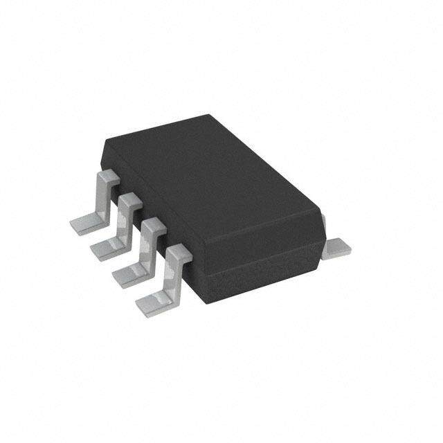
| 产品图片 |
|
| rohs | 符合RoHS无铅 / 符合限制有害物质指令(RoHS)规范要求 |
| 产品系列 | 数字电位计 IC,Intersil X95820WV14IZ-2.7XDCP™ |
| 数据手册 | |
| 产品型号 | X95820WV14IZ-2.7 |
| POT数量 | Dual |
| 产品种类 | 数字电位计 IC |
| 供应商器件封装 | 14-TSSOP |
| 其它名称 | X95820WV14IZ27 |
| 包装 | 管件 |
| 商标 | Intersil |
| 存储器类型 | 非易失 |
| 安装类型 | 表面贴装 |
| 封装 | Tube |
| 封装/外壳 | 14-TSSOP(0.173",4.40mm 宽) |
| 封装/箱体 | TSSOP-14 |
| 工作温度 | -40°C ~ 85°C |
| 工作电源电压 | 3.3 V |
| 工厂包装数量 | 95 |
| 弧刷存储器 | Non Volatile |
| 抽头 | 256 |
| 接口 | I²C(设备位址) |
| 数字接口 | Serial (I2C) |
| 最大工作温度 | + 85 C |
| 最小工作温度 | - 40 C |
| 标准包装 | 95 |
| 每POT分接头 | 256 |
| 温度系数 | 标准值 ±45 ppm/°C |
| 电压-电源 | 2.7 V ~ 5.5 V |
| 电源电压-最大 | 5.5 V |
| 电源电压-最小 | 2.7 V |
| 电源电流 | 1 mA |
| 电路数 | 2 |
| 电阻 | 10 KOhms |
| 电阻(Ω) | 10k |
| 系列 | X9582 |


- 商务部:美国ITC正式对集成电路等产品启动337调查
- 曝三星4nm工艺存在良率问题 高通将骁龙8 Gen1或转产台积电
- 太阳诱电将投资9.5亿元在常州建新厂生产MLCC 预计2023年完工
- 英特尔发布欧洲新工厂建设计划 深化IDM 2.0 战略
- 台积电先进制程称霸业界 有大客户加持明年业绩稳了
- 达到5530亿美元!SIA预计今年全球半导体销售额将创下新高
- 英特尔拟将自动驾驶子公司Mobileye上市 估值或超500亿美元
- 三星加码芯片和SET,合并消费电子和移动部门,撤换高东真等 CEO
- 三星电子宣布重大人事变动 还合并消费电子和移动部门
- 海关总署:前11个月进口集成电路产品价值2.52万亿元 增长14.8%


PDF Datasheet 数据手册内容提取
DATASHEET X95820 FN8212 2 Dual Digital Controlled Potentiometers (XDCP™) Low Noise/Low Power/I C Rev 2.00 Bus/256 Taps July 18, 2006 The X95820 integrates two digitally controlled Features potentiometers (XDCP) on a monolithic CMOS integrated • Two potentiometers in one package circuit. • 256 resistor taps-0.4% resolution The digitally controlled potentiometers are implemented with a combination of resistor elements and CMOS switches. The • I2C serial interface position of the wipers are controlled by the user through the - Three address pins, up to eight devices/bus I2C bus interface. Each potentiometer has an associated • Wiper resistance: 70 typical @ 3.3V volatile Wiper Register (WR) and a non-volatile Initial Value Register (IVR), that can be directly written to and read by the • Non-volatile storage of wiper position user. The contents of the WR controls the position of the • Standby current < 5µA max wiper. At power up the device recalls the contents of the two DCP’s IVR to the corresponding WRs. • Power supply: 2.7V to 5.5V • 50k, 10k total resistance The DCPs can be used as three-terminal potentiometers or as two-terminal variable resistors in a wide variety of • High reliability applications including control, parameter adjustments, and - Endurance: 150,000 data changes per bit per register signal processing. - Register data retention: 50 years @ T 75°C Ordering Information • 14 Ld TSSOP • Pb-free plus anneal available (RoHS compliant) PART RESISTANCE PART NUMBER MARKING OPTION PACKAGE Pinouts X95820WV14I-2.7* X95820WV G 10k 14 Ld TSSOP X95820 X95820WV14IZ-2.7* X95820WV Z G 10k 14 Ld TSSOP (14 LD TSSOP) (Note) (Pb-free) TOP VIEW X95820UV14I-2.7* X95820UV G 50k 14 Ld TSSOP VCC 1 14 A1 X95820UV14IZ-2.7* X95820UV Z G 50k 14 Ld TSSOP WP 2 13 A0 (Note) (Pb-free) RH0 3 12 RH1 *Add "T1" suffix for tape and reel. RL0 4 11 RL1 NOTE: Intersil Pb-free plus anneal products employ special Pb-free RW0 5 10 RW1 material sets; molding compounds/die attach materials and 100% A2 6 9 GND matte tin plate termination finish, which are RoHS compliant and compatible with both SnPb and Pb-free soldering operations. Intersil SCL 7 8 SDA Pb-free products are MSL classified at Pb-free peak reflow temperatures that meet or exceed the Pb-free requirements of IPC/JEDEC J STD-020. FN8212 Rev 2.00 Page 1 of 12 July 18, 2006
X95820 Block Diagram VCC I2C RH1 POWER-UP, INTERFACE SDA CIONNTTERROFAL CAEN,D WR1 RW1 SCL STATUS LOGIC RL1 A2 A1 RH0 A0 NON-VOLATILE WR0 RW0 REGISTERS RL0 WP GND PiN Descriptions PIN SYMBOL DESCRIPTION 1 VCC Power supply pin 2 WP Hardware write protection pin. Active low. Prevents any “Write” operation of the I2C interface. 3 RH0 “High” terminal of DCP0 4 RL0 “Low” terminal of DCP0 5 RW0 “Wiper” terminal of DCP0 6 A2 Device address for the I2C interface 7 SCL I2C interface clock 8 SDA Serial data I/O for the I2C interface 9 GND Ground 10 RW1 “Wiper” terminal of DCP1 11 RL1 “Low” terminal of DCP1 12 RH1 “High” terminal of DCP1 13 A0 Device address for the I2C interface 14 A1 Device address for the I2C interface FN8212 Rev 2.00 Page 2 of 12 July 18, 2006
X95820 Absolute Maximum Ratings Recommended Operating Conditions Storage Temperature. . . . . . . . . . . . . . . . . . . . . . . .-65C to +150C Temperature Range (Industrial). . . . . . . . . . . . . . . . . .-40°C to 85°C Voltage at Any Digital Interface Pin VCC . . . . . . . . . . . . . . . . . . . . . . . . . . . . . . . . . . . . . . . .2.7V to 5.5V with Respect to GND. . . . . . . . . . . . . . . . . . . . . . .-0.3V to VCC+0.3 Power Rating of Each DCP. . . . . . . . . . . . . . . . . . . . . . . . . . . .5mW VCC . . . . . . . . . . . . . . . . . . . . . . . . . . . . . . . . . . . . . . . .-0.3V to +6V Wiper Current of Each DCP. . . . . . . . . . . . . . . . . . . . . . . . . .±3.0mA Voltage at Any DCP Pin with Respect to GND . . . . . . -0.3V to VCC Lead Temperature (soldering, 10s) . . . . . . . . . . . . . . . . . . . . .300C IW (10s) . . . . . . . . . . . . . . . . . . . . . . . . . . . . . . . . . . . . . . . . . . ±6mA CAUTION: Stresses above those listed under “Absolute Maximum Ratings” may cause permanent damage to the device. This is a stress rating only; functional operation of the device (at these or any other conditions above those listed in the operational sections of this specification) is not implied. Exposure to absolute maximum rating conditions for extended periods may affect device reliability. Analog Specifications Over recommended operating conditions unless otherwise stated. TYP SYMBOL PARAMETER TEST CONDITIONS MIN (Note 1) MAX UNIT RTOTAL RH to RL Resistance W, U versions respectively 10, 50 k RH to RL Resistance Tolerance -20 +20 % RW Wiper Resistance VCC = 3.3V @ 25°C 70 200 Wiper current = VCC/RTOTAL CH/CL/CW Potentiometer Capacitance (Note 15) 10/10/25 pF ILkgDCP Leakage on DCP Pins (Note 15) Voltage at pin from GND to VCC 0.1 1 µA VOLTAGE DIVIDER MODE (0V @ RLi; VCC @ RHi; measured at RWi, unloaded; i = 0 or 1) INL (Note 6) Integral Non-linearity -1 1 LSB (Note 2) DNL (Note 5) Differential Non-linearity Monotonic over all tap positions -0.5 0.5 LSB (Note 2) ZSerror Zero-scale Error U option 0 1 7 LSB (Note 3) (Note 2) W option 0 0.5 2 FSerror Full-scale Error U option -7 -1 0 LSB (Note 4) (Note 2) W option -2 -1 0 VMATCH DCP to DCP Matching Any two DCPs at same tap position, same -2 2 LSB (Note 7) voltage at all RH terminals, and same (Note 2) voltage at all RL terminals TCV (Note 8) Ratiometric Temperature Coefficient DCP Register set to 80 hex ±4 ppm/°C RESISTOR MODE (Measurements between RWi and RLi with RHi not connected, or between RWi and RHi with RLi not connected. i = 0 or 1) RINL Integral Non-linearity DCP register set between 20 hex and -1 1 MI (Note 12) FF hex. Monotonic over all tap positions (Note 9) RDNL Differential Non-linearity -0.5 0.5 MI (Note 11) (Note 9) Roffset Offset DCP Register set to 00 hex, U option 0 1 7 MI (Note 10) (Note 9) DCP Register set to 00 hex, W option 0 0.5 2 MI (Note 9) RMATCH DCP to DCP Matching Any two DCPs at the same tap position with -2 2 MI (Note 13) the same terminal voltages. (Note 9) TCR Resistance Temperature Coefficient DCP register set between 20 hex and FF ±45 ppm/°C (Note 14) hex FN8212 Rev 2.00 Page 3 of 12 July 18, 2006
X95820 Operating Specifications Over the recommended operating conditions unless otherwise specified. TYP SYMBOL PARAMETER TEST CONDITIONS MIN (Note 1) MAX UNITS ICC1 VCC Supply Current fSCL = 400kHz;SDA = Open; (for I2C, 1 mA (Volatile write/read) Active, Read and Volatile Write States only) ICC2 VCC Supply Current fSCL = 400kHz; SDA = Open; (for I2C, 3 mA (nonvolatile write) Active, Nonvolatile Write State only) ISB VCC Current (standby) VCC = +5.5V, I2C Interface in Standby State 5 µA VCC = +3.6V, I2C Interface in Standby State 2 µA ILkgDig Leakage Current, at Pins A0, Voltage at pin from GND to VCC -10 10 µA A1, A2, SDA, SCL, and WP Pins tDCP DCP Wiper Response Time SCL falling edge of last bit of DCP Data Byte to 1 µs (Note 15) wiper change Vpor Power-on Recall Voltage Minimum VCC at which memory recall occurs 1.8 2.6 V VccRamp VCC Ramp Rate 0.2 V/ms tD (Note 15) Power-up Delay VCC above Vpor, to DCP Initial Value Register recall 3 ms completed, and I2C Interface in standby state EEPROM SPECS EEPROM Endurance 150,000 Cycles EEPROM Retention Temperature 75°C 50 Years SERIAL INTERFACE SPECS VIL WP, A2, A1, A0, SDA, and -0.3 0.3*Vcc V SCL input buffer LOW voltage VIH WP, A2, A1, A0, SDA, and 0.7*Vcc Vcc+0.3 V SCL Input Buffer HIGH Voltage Hysterisis SDA and SCL input buffer 0.05* V (Note 15) hysterisis Vcc VOL SDA Output Buffer LOW 0 0.4 V (Note 15) Voltage, Sinking 4mA Cpin WP, A2, A1, A0, SDA, and 10 pF (Note 15) SCL Pin Capacitance fSCL SCL Frequency 400 kHz tIN Pulse Width Suppression Any pulse narrower than the max spec is 50 ns (Note 15) Time at SDA and SCL Inputs suppressed. tAA SCL Falling Edge to SDA SCL falling edge crossing 30% of VCC, until SDA 900 ns (Note 15) Output Data Valid exits the 30% to 70% of VCC window. tBUF Time the Bus Must be Free SDA crossing 70% of VCC during a STOP condition, 1300 ns (Note 15) Before the Start of a New to SDA crossing 70% of VCC during the following Transmission START condition. tLOW Clock LOW Time Measured at the 30% of VCC crossing. 1300 ns tHIGH Clock HIGH Time Measured at the 70% of VCC crossing. 600 ns tSU:STA START Condition Setup SCL rising edge to SDA falling edge. Both crossing 600 ns Time 70% of VCC. tHD:STA START Condition Hold Time From SDA falling edge crossing 30% of VCC to SCL 600 ns falling edge crossing 70% of VCC. FN8212 Rev 2.00 Page 4 of 12 July 18, 2006
X95820 Operating Specifications Over the recommended operating conditions unless otherwise specified. (Continued) TYP SYMBOL PARAMETER TEST CONDITIONS MIN (Note 1) MAX UNITS tSU:DAT Input Data Setup Time From SDA exiting the 30% to 70% of VCC 100 ns window, to SCL rising edge crossing 30% of VCC tHD:DAT Input Data Hold Time From SCL rising edge crossing 70% of VCC to SDA 0 ns entering the 30% to 70% of VCC window. tSU:STO STOP Condition Setup Time From SCL rising edge crossing 70% of VCC, to SDA 600 ns rising edge crossing 30% of VCC. tHD:STO STOP Condition Setup Time From SDA rising edge to SCL falling edge. Both 600 ns crossing 70% of VCC. tDH (Note 15) Output Data Hold Time From SCL falling edge crossing 30% of VCC, until 0 ns SDA enters the 30% to 70% of VCC window. tR (Note 15) SDA and SCL Rise Time From 30% to 70% of VCC 20 + 250 ns 0.1 * Cb tF (Note 15) SDA and SCL Fall Time From 70% to 30% of VCC 20 + 250 ns 0.1 * Cb Cb (Note 15) Capacitive Loading of SDA Total on-chip and off-chip 10 400 pF or SCL Rpu (Note 15) SDA and SCL Bus Pull-up Maximum is determined by tR and tF. 1 k resIstor Off-chip For Cb = 400pF, max is about 2~2.5k. For Cb = 40pF, max is about 15~20k tWP Non-volatile Write Cycle 12 20 ms (Notes 15, 16) Time tSU:WPA A2, A1, A0, and WP Setup Before START condition 600 ns Time tHD:WPA A2, A1, A0, and WP Hold After STOP condition 600 ns Time SDA vs. SCL Timing tF tHIGH tLOW tR SCL tSU:DAT tSU:STA tHD:DAT tSU:STO tHD:STA SDA (INPUT TIMING) tAA tDH tBUF SDA (OUTPUT TIMING) WP, A0, A1, and A2 Pin Timing START STOP SCL Clk 1 SDA IN tSU:WPA tHD:WPA WP, A0, A1, or A2 FN8212 Rev 2.00 Page 5 of 12 July 18, 2006
X95820 NOTES: 1. Typical values are for TA = 25°C and 3.3V supply voltage. 2. LSB: [V(RW)255 - V(RW)0] / 255. V(RW)255 and V(RW)0 are V(RW) for the DCP register set to FF hex and 00 hex respectively. LSB is the incremental voltage when changing from one tap to an adjacent tap. 3. ZS error = V(RW)0 / LSB. 4. FS error = [V(RW)255 - VCC] / LSB. 5. DNL = [V(RW)i - V(RW)i-1] / LSB-1, for i = 1 to 255. i is the DCP register setting. 6. INL = [V(RW)i – (i • LSB – V(RW)0)]/LSB for i = 1 to 255. 7. VMATCH = [V(RWx)i - V(RWy)i] / LSB, for i = 0 to 255, x = 0 to 1 and y = 0 to 1. MaxVRWi–MinVRWi 106 8. TC = --------------------------------------------------------------------------------------------------------------- V MaxVRW+MinVRW2 125°C i i for i = 16 to 240 decimal, T = -40°C to 85°C. Max( ) is the maximum value of the wiper voltage and Min ( ) is the minimum value of the wiper voltage over the temperature range. 9. MI = |R255 - R0| / 255. R255 and R0 are the measured resistances for the DCP register set to FF hex and 00 hex respectively. 10. Roffset = R0 / MI, when measuring between RW and RL. Roffset = R255 / MI, when measuring between RW and RH. 11. RDNL = (Ri - Ri-1) / MI, for i = 32 to 255. 12. RINL = [Ri - (MI • i) - R0] / MI, for i = 32 to 255. 13. RMATCH = (Ri,x - Ri,y) / MI, for i = 0 to 255, x = 0 to 1 and y = 0 to 1. 6 14. TC = -------M-----a----x------R-----i-----–-----M-----i--n------R-----i-------------1----0--------- R MaxRi+MinRi2 125°C for i = 32 to 255, T = -40°C to 85°C. Max( ) is the maximum value of the resistance and Min ( ) is the minimum value of the resistance over the temperature range. 15. This parameter is not 100% tested. 16. tWC is the minimum cycle time to be allowed for any non-volatile Write by the user, unless Acknowledge Polling is used. It is the time from a valid STOP condition at the end of a Write sequence of a I2C serial interface Write operation, to the end of the self-timed internal non-volatile write cycle. Typical Performance Curves 160 1.8 VCC = 2.7, T = 85°C 140 1.6 VCC = 2.7, T = -40°C VCC = 2.7, T = 25°C 1.4 )120 CE (100 µA) 1.2 AN (C 1.0 -40°C T 80 C SIS BY I 0.8 E 60 D 85°C R N 0.6 R A PE 40 ST 0.4 WI 20 VCC = 5.5, T = 85°C 0.2 VCC = 5.5, T = -40°C VCC = 5.5, T = 25°C 25°C 0 0.0 0 50 100 150 200 250 2.7 3.2 3.7 4.2 4.7 5.2 TAP POSITION (DECIMAL) VCC (V) FIGURE 1. WIPER RESISTANCE vs TAP POSITION FIGURE 2. STANDBY ICC vs VCC [ I(RW) = VCC/RTOTAL ] FOR 50k (U) FN8212 Rev 2.00 Page 6 of 12 July 18, 2006
X95820 Typical Performance Curves (Continued) 0.01.52 VCC = 2.7, T V=C 2C5 °=C 5.5, T = -40°C VCC = 2.7, T = -40°C 00..23 VCC = 5.5, T = -4V0C°CC = 2.7, T = -40°C VCC = 5.5, T = 85°C 0.1 0.1 0.05 B) B) L (LS 0 L (LS 0 VCC = 2.7, T = 25°C DN-0.05 IN-0.1 VCC = 2.7, T = 85°C -0.1 VCC = 5.5, T = 25°C VCC = 5.5, T = 25°C -0.15 VCC = 2.7, T = 85°C VCC = 5.5, T = 85°C -0.2 -0.2 -0.3 0 50 100 150 200 250 0 50 100 150 200 250 TAP POSITION (DECIMAL) TAP POSITION (DECIMAL) FIGURE 3. DNL vs TAP POSITION IN VOLTAGE DIVIDER FIGURE 4. INL vs TAP POSITION IN VOLTAGE DIVIDER MODE FOR 10k (W) MODE FOR 10k (W) 0.4 0 -0.1 0.35 -0.2 VCC = 5.5V -0.3 error (LSB)0.02.53 2.7V Serror (LSB)---000...654 VCC = 2.7V S F Z -0.7 0.2 -0.8 5.5V -0.9 0.15 -1 -40 -20 0 20 40 60 80 -40 -20 0 20 40 60 80 TEMPERATURE (°C) TEMPERATURE (°C) FIGURE 5. ZSerror vs TEMPERATURE FIGURE 6. FSerror vs TEMPERATURE 0.3 0.5 VCC = 2.7, T = 25°C 0.4 VCC = 2.7, T = 25°C 0.2 VCC = 5.5, T = 25°C 0.3 0.2 VCC = 5.5, T = -40°C 0.1 0.1 LSB) 0 LSB) 0 VCC = 5.5, T = 85°C NL ( NL (-0.1 D-0.1 I-0.2 VCC = 5.5, T = 85°C -0.3 -0.2 VCC = 2.7, T = -40°C VCC = 2.7, T = 85°C -0.4 VCC = 2.7, T = 85°C VCC = 5.5, T = -40°C -0.5 VCC = 5.5, T = 25°C VCC = 2.7, T = -40°C -0.3 32 82 132 182 232 32 82 132 182 232 TAP POSITION (DECIMAL) TAP POSITION (DECIMAL) FIGURE 7. DNL vs TAP POSITION IN Rheostat MODE FOR FIGURE 8. INL vs TAP POSITION IN Rheostat MODE FOR 50k (U) 50k (U) FN8212 Rev 2.00 Page 7 of 12 July 18, 2006
X95820 Typical Performance Curves (Continued) 1.50 20 %) E ( 1.00 G N 10 A H 0.50 COTAL0.00 5.5V 2.7V pm/°C) 0 D RT C (p N-0.50 T E O -10 T D -1.00 N E -1.50 -20 -40 -20 0 20 40 60 80 32 82 132 182 232 TEMPERATURE (°C) TAP POSITION (DECIMAL) FIGURE 9. END TO END RTOTAL % CHANGE vs FIGURE 10. TC FOR VOLTAGE DIVIDER MODE IN ppm TEMPERATURE 35 INPUT 25 15 C) pm/° 5 OUTPUT p C ( T -5 Tap Position = Mid Point -15 RTOTAL = 9.4K -25 32 57 82 107 132 157 182 207 232 TAP POSITION (DECIMAL) FIGURE 12. FREQUENCY RESPONSE (2.2MHz) FIGURE 11. TC FOR Rheostat MODE IN ppm Signal at Wiper (Wiper Unloaded) SCL Signal at Wiper (Wiper Unloaded Movement From ffh to 00h) Wiper Movement Mid Point From 80h to 7fh FIGURE 13. MIDSCALE GLITCH, CODE 80h TO 7Fh (WIPER 0) FIGURE 14. LARGE SIGNAL SETTLING TIME FN8212 Rev 2.00 Page 8 of 12 July 18, 2006
X95820 Principles of Operation When the byte at address 8 is all zeroes, which is the default at power up: The X95820 in as integrated circuit incorporating two DCPs with their associated registers, non-volatile memory, and a I2C • A read operation to addresses 0 or 1 outputs the value of the serial interface providing direct communication between a host non-volatile IVRs. and the potentiometers and memory. • A write operation to addresses 0 or 1 writes the same value to the WR and IVR of the corresponding DCP. DCP Description When the byte at address 8 is 80h (128 decimal): Each DCP is implemented with a combination of resistor elements and CMOS switches. The physical ends of each DCP • A read operation to addresses 0 or 1 outputs the value of the are equivalent to the fixed terminals of a mechanical volatile WR. potentiometer (RH and RL pins). The RW pin of each DCP is • A write operation to addresses 0 or 1only writes to the connected to intermediate nodes, and is equivalent to the corresponding volatile WR. wiper terminal of a mechanical potentiometer. The position of It is not possible to write to an IVR without writing the same the wiper terminal within the DCP is controlled by an 8-bit value to its corresponding WR. volatile Wiper Register (WR). Each DCP has its own WR. When the WR of a DCP contains all zeroes (WR<7:0>: 00h), 00h and 80h are the only values that should be written to its wiper terminal (RW) is closest to its “Low” terminal (RL). address 8. All other values are reserved and must not be When the WR of a DCP contains all ones (WR<7:0>: FFh), its written to address 8. wiper terminal (RW) is closest to its “High” terminal (RH). As To access the general purpose bytes at addresses 2, 3, 4, 5, or the value of the WR increases from all zeroes (00h) to all ones 6, the value at address 8 must be all zeros. (255 decimal), the wiper moves monotonically from the position closest to RL to the closest to RH. At the same time, The X95820 is pre-programmed with 80h in the two IVRs. the resistance between RW and RL increases monotonically, TABLE 1. MEMORY MAP while the resistance between RH and RW decreases ADDRESS NON-VOLATILE VOLATILE monotonically. 8 - Access Control While the X95820 is being powered up, all two WRs are reset 7 Reserved to 80h (128 decimal), which locates RW roughly at the center between RL and RH. Soon after the power supply voltage 6 General Purpose Not Available becomes large enough for reliable non-volatile memory 5 4 reading, the X95820 reads the value stored on two different 3 non-volatile Initial Value Registers (IVRs) and loads them into 2 their corresponding WRs. 1 IVR1 WR1 The WRs and IVRs can be read or written directly using the 0 IVR0 WR0 I2C serial interface as described in the following sections. WR: Wiper Register, IVR: Initial value Register. Memory Description 2 I C Serial Interface The X95820 contains eight non-volatile bytes. they are accessed by I2C interface operations with Address Bytes 0 The X95820 supports a bidirectional I2C bus oriented protocol. through 7 decimal. The first two non-volatile bytes at The protocol defines any device that sends data onto the bus addresses 0 and 1 contain the initial value loaded at power-up as a transmitter and the receiving device as the receiver. The into the volatile Wiper Registers (WRs) of DCP0 and DCP1 device controlling the transfer is a master and the device being respectively. Bytes at addresses 2, 3, 4, 5, and 6 are available controlled is the slave. The master always initiates data to the user as general purpose registers. The byte at address 7 transfers and provides the clock for both transmit and receive is reserved; the user should not write to it, and its value should operations. Therefore, the X95820 operates as a slave device be ignored if read. in all applications. The volatile WR, and the non-volatile Initial Value Register All communication over the I2C interface is conducted by (IVR) of a DCP are accessed with the same Address Byte. sending the MSB of each byte of data first. A volatile byte at address 8 decimal, controls what byte is read Protocol Conventions or written when accessing DCP registers: the WR, the IVR, or Data states on the SDA line can change only during SCL LOW both. periods. SDA state changes during SCL HIGH are reserved for indicating START and STOP conditions (See Figure 15). On power up of the X95820 the SDA pin is in the input mode. FN8212 Rev 2.00 Page 9 of 12 July 18, 2006
X95820 All I2C interface operations must begin with a START SDA line LOW to acknowledge the reception of the eight bits of condition, which is a HIGH to LOW transition of SDA while SCL data (See Figure 16). is HIGH. The X95820 continuously monitors the SDA and SCL The X95820 responds with an ACK after recognition of a lines for the START condition and does not respond to any START condition followed by a valid Identification Byte, and command until this condition is met (See Figure 15). A START once again after successful receipt of an Address Byte. The condition is ignored during the power up sequence and during X95820 also responds with an ACK after receiving a Data Byte internal non-volatile write cycles. of a write operation. The master must respond with an ACK All I2C interface operations must be terminated by a STOP after receiving a Data Byte of a read operation condition, which is a LOW to HIGH transition of SDA while SCL A valid Identification Byte contains 1010 as the four MSBs, and is HIGH (See Figure 15). A STOP condition at the end of a the following three bits matching the logic values present at read operation, or at the end of a write operation to volatile pins A2, A1, and A0. The LSB in the Read/Write bit. Its value is bytes only places the device in its standby mode. A STOP “1” for a Read operation, and “0” for a Write operation (See condition during a write operation to a non-volatile byte, Table 2). initiates an internal non-volatile write cycle. The device enters its standby state when the internal non-volatile write cycle is TABLE 2. IDENTIFICATION BYTE FORMAT completed. Logic values at pins A2, A1, and A0 respectively An ACK, Acknowledge, is a software convention used to indicate a successful data transfer. The transmitting device, 1 0 1 0 A2 A1 A0 R/W either master or slave, releases the SDA bus after transmitting (MSB) (LSB) eight bits. During the ninth clock cycle, the receiver pulls the SCL SDA START DATA DATA DATA STOP STABLE CHANGE STABLE FIGURE 15. VALID DATA CHANGES, START, AND STOP CONDITIONS SCL from Master 1 8 9 SDA Output from High Impedance Transmitter SDA Output from High Impedance Receiver START ACK FIGURE 16. ACKNOWLEDGE RESPONSE FROM RECEIVER Write S Signals from the t S Master a Identification Address Data t r Byte Byte Byte o t p Signal at SDA 1 0 1 0A2A1A00 0 0 0 0 Signals from the A A A X95820 C C C K K K FIGURE 17. BYTE WRITE SEQUENCE FN8212 Rev 2.00 Page 10 of 12 July 18, 2006
X95820 Write Operation Control Register, at the falling edge of the SCL pulse that loads the last bit (LSB) of the Data Byte. If the Address Byte is A Write operation requires a START condition, followed by a between 0 and 6 (inclusive), and the Access Control Register valid Identification Byte, a valid Address Byte, a Data Byte, and is all zeros (default), then the STOP condition initiates the a STOP condition. After each of the three bytes, the X95820 internal write cycle to non-volatile memory. responds with an ACK. At this time, if the Data Byte is to be written only to volatile registers, then the device enters its Read Operation standby state. If the Data Byte is to be written also to non- volatile memory, the X95820 begins its internal write cycle to A Read operation consists of a three byte instruction followed non-volatile memory. During the internal non-volatile write by one or more Data Bytes (See Figure 18). The master cycle, the device ignores transitions at the SDA and SCL pins, initiates the operation issuing the following sequence: a and the SDA output is at a high impedance state. When the START, the Identification byte with the R/W bit set to “0”, an internal non-volatile write cycle is completed, the X95820 Address Byte, a second START, and a second Identification enters its standby state (See Figure 17). byte with the R/W bit set to “1”. After each of the three bytes, the X95820 responds with an ACK. Then the X95820 transmits The byte at address 00001000 bin (8 decimal) determines if Data Bytes as long as the master responds with an ACK during the Data Byte is to be written to volatile and/or non-volatile the SCL cycle following the eight bit of each byte. The master memory. See “Memory Description” on page 9. terminates the read operation (issuing a STOP condition) following the last bit of the last Data Byte (See Figure 18). Data Protection The Data Bytes are from the memory location indicated by an The WP pin has to be at logic HIGH to perform any Write internal pointer. This pointer initial value is determined by the operation to the device. When the WP is active (LOW) the Address Byte in the Read operation instruction, and device ignores Data Bytes of a Write Operation, does not increments by one during transmission of each Data Byte. respond to the Data Bytes with an ACK, and instead, goes to After reaching the memory location 01Fh (8 decimal) the its standby state waiting for a new START condition. pointer “rolls over” to 00h, and the device continues to output A STOP condition also acts as a protection of non-volatile data for each ACK received. memory. A valid Identification Byte, Address Byte, and total The byte at address 00001000 bin (8 decimal) determines if number of SCL pulses act as a protection of both volatile and the Data Bytes being read are from volatile or non-volatile non-volatile registers. During a Write sequence, the Data Byte memory. See “Memory Description” on page 9. is loaded into an internal shift register as it is received. If the Address Byte is 0, 1, or 8 decimal, the Data Byte is transferred to the appropriate Wiper Register (WR) or to the Access S Identification S Identification Signals t Byte t Byte S froMmas ttheer art Rw/With=0 AdBdyrteess art Rw/With=1 AC AC opt K K Signal at SDA 1 0 1 0 0 1 0 1 0 1 A A A Signals from the C C C Slave K K K First Read Data Last Read Data Byte Byte FIGURE 18. READ SEQUENCE FN8212 Rev 2.00 Page 11 of 12 July 18, 2006
X95820 Thin Shrink Small Outline Plastic Packages (TSSOP) M14.173 N 14 LEAD THIN SHRINK SMALL OUTLINE PLASTIC INDEX E 0.25(0.010) M B M PACKAGE AREA E1 INCHES MILLIMETERS GAUGE -B- PLANE SYMBOL MIN MAX MIN MAX NOTES A - 0.047 - 1.20 - 1 2 3 A1 0.002 0.006 0.05 0.15 - L 0.05(0.002) SEATING PLANE 0.25 A2 0.031 0.041 0.80 1.05 - 0.010 -A- b 0.0075 0.0118 0.19 0.30 9 D A c 0.0035 0.0079 0.09 0.20 - D 0.195 0.199 4.95 5.05 3 -C- E1 0.169 0.177 4.30 4.50 4 e A2 A1 c e 0.026 BSC 0.65 BSC - b 0.10(0.004) E 0.246 0.256 6.25 6.50 - 0.10(0.004) M C A M B S L 0.0177 0.0295 0.45 0.75 6 N 14 14 7 NOTES: 0o 8o 0o 8o - 1. These package dimensions are within allowable dimensions of Rev. 2 4/06 JEDEC MO-153-AC, Issue E. 2. Dimensioning and tolerancing per ANSI Y14.5M-1982. 3. Dimension “D” does not include mold flash, protrusions or gate burrs. Mold flash, protrusion and gate burrs shall not exceed 0.15mm (0.006 inch) per side. 4. Dimension “E1” does not include interlead flash or protrusions. Inter- lead flash and protrusions shall not exceed 0.15mm (0.006 inch) per side. 5. The chamfer on the body is optional. If it is not present, a visual index feature must be located within the crosshatched area. 6. “L” is the length of terminal for soldering to a substrate. 7. “N” is the number of terminal positions. 8. Terminal numbers are shown for reference only. 9. Dimension “b” does not include dambar protrusion. Allowable dambar protrusion shall be 0.08mm (0.003 inch) total in excess of “b” dimen- sion at maximum material condition. Minimum space between protru- sion and adjacent lead is 0.07mm (0.0027 inch). 10. Controlling dimension: MILLIMETER. Converted inch dimensions are not necessarily exact. (Angles in degrees) © Copyright Intersil Americas LLC 2005-2006. All Rights Reserved. All trademarks and registered trademarks are the property of their respective owners. For additional products, see www.intersil.com/en/products.html Intersil products are manufactured, assembled and tested utilizing ISO9001 quality systems as noted in the quality certifications found at www.intersil.com/en/support/qualandreliability.html Intersil products are sold by description only. Intersil may modify the circuit design and/or specifications of products at any time without notice, provided that such modification does not, in Intersil's sole judgment, affect the form, fit or function of the product. Accordingly, the reader is cautioned to verify that datasheets are current before placing orders. Information furnished by Intersil is believed to be accurate and reliable. However, no responsibility is assumed by Intersil or its subsidiaries for its use; nor for any infringements of patents or other rights of third parties which may result from its use. No license is granted by implication or otherwise under any patent or patent rights of Intersil or its subsidiaries. For information regarding Intersil Corporation and its products, see www.intersil.com FN8212 Rev 2.00 Page 12 of 12 July 18, 2006