ICGOO在线商城 > 集成电路(IC) > 数据采集 - 数字电位器 > AD5232BRUZ100

 Datasheet下载
- 型号: AD5232BRUZ100
- 制造商: Analog
- 库位|库存: xxxx|xxxx
- 要求:
| 数量阶梯 | 香港交货 | 国内含税 |
| +xxxx | $xxxx | ¥xxxx |
查看当月历史价格
查看今年历史价格
AD5232BRUZ100产品简介:
ICGOO电子元器件商城为您提供AD5232BRUZ100由Analog设计生产,在icgoo商城现货销售,并且可以通过原厂、代理商等渠道进行代购。 AD5232BRUZ100价格参考¥21.37-¥22.16。AnalogAD5232BRUZ100封装/规格:数据采集 - 数字电位器, Digital Potentiometer 100k Ohm 2 Circuit 256 Taps SPI Interface 16-TSSOP。您可以下载AD5232BRUZ100参考资料、Datasheet数据手册功能说明书,资料中有AD5232BRUZ100 详细功能的应用电路图电压和使用方法及教程。
AD5232BRUZ100 是由 Analog Devices Inc.(亚德诺半导体)生产的一款数字电位器,属于数据采集系统中的关键元件。它具有非易失性存储功能,能够保存设置值,即使断电后也能恢复到之前的配置。以下是该型号的一些典型应用场景:

 1. 音频设备
   - 在音频设备中,AD5232BRUZ100 可用于音量控制、增益调节或均衡器调整。其非易失性特性确保用户自定义的音量或增益设置在设备重启后仍然有效。
   - 例如:耳机放大器、音响系统、调音台等。

 2. 工业控制系统
   - 用于工业自动化设备中的信号调理和增益调整。例如,在传感器信号放大电路中,可以通过数字电位器动态调整放大倍数,以适应不同的输入信号范围。
   - 应用场景包括可编程逻辑控制器(PLC)、数据采集模块和过程控制系统。

 3. 医疗设备
   - 在医疗设备中,如心率监测仪、血压计或超声波设备,AD5232BRUZ100 可用于校准和补偿电路。通过数字化调节,可以实现更高的精度和稳定性。
   - 其非易失性特点也使得设备在出厂校准后无需频繁重新调整。

 4. 通信设备
   - 在通信领域,AD5232BRUZ100 可用于调节射频(RF)电路中的增益或匹配阻抗。例如,在无线模块或基站中,它可以动态调整功率放大器的输出水平。
   - 此外,还可以用于滤波器调谐,优化信号传输质量。

 5. 消费电子产品
   - 在便携式电子设备中,如智能手表、健康手环或其他物联网设备,AD5232BRUZ100 可用于电源管理电路中的电压调节,以延长电池寿命并优化性能。

 6. 测试与测量仪器
   - 在示波器、信号发生器或多用途测试仪中,AD5232BRUZ100 能够提供精确的电阻调节功能,用于校准或调整测量范围。
   - 它的高分辨率和低漂移特性使其非常适合需要高精度的应用场合。

 总结
AD5232BRUZ100 的主要优势在于其高可靠性、非易失性和易于集成的特点。无论是消费类电子产品还是工业级应用,这款数字电位器都能为用户提供灵活且高效的解决方案,满足多种动态调节需求。
| 参数 | 数值 |
| 产品目录 | 集成电路 (IC)半导体 |
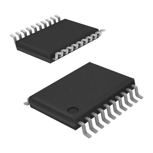
| 描述 | IC DGTL POT DUAL 256POS 16-TSSOP数字电位计 IC IC Dual 8Bit EEMEM |
| DevelopmentKit | EVAL-AD5232SDZ |
| 产品分类 | |
| 品牌 | Analog Devices |
| 产品手册 | |
| 产品图片 |
|
| rohs | 符合RoHS无铅 / 符合限制有害物质指令(RoHS)规范要求 |
| 产品系列 | 数字电位计 IC,Analog Devices AD5232BRUZ100- |
| 数据手册 | |
| 产品型号 | AD5232BRUZ100 |
| PCN设计/规格 | |
| PCN过时产品 | |
| POT数量 | Dual |
| 产品种类 | 数字电位计 IC |
| 供应商器件封装 | 16-TSSOP |
| 包装 | 管件 |
| 商标 | Analog Devices |
| 存储器类型 | 非易失 |
| 安装类型 | 表面贴装 |
| 安装风格 | SMD/SMT |
| 容差 | - 40 % to + 20 % |
| 封装 | Tube |
| 封装/外壳 | 16-TSSOP(0.173",4.40mm 宽) |
| 封装/箱体 | TSSOP-16 |
| 工作温度 | -40°C ~ 85°C |
| 工作电源电压 | 2.7 V |
| 工厂包装数量 | 96 |
| 弧刷存储器 | Non Volatile |
| 抽头 | 256 |
| 接口 | 4 线 SPI(芯片选择) |
| 数字接口 | SPI |
| 最大工作温度 | + 85 C |
| 最小工作温度 | - 40 C |
| 标准包装 | 96 |
| 每POT分接头 | 256 |
| 温度系数 | 300 PPM / C |
| 电压-电源 | 2.7 V ~ 5.5 V, ±2.25 V ~ 2.75 V |
| 电源电压-最大 | 5.5 V |
| 电源电压-最小 | 2.7 V |
| 电源电流 | 3.5 uA |
| 电路数 | 2 |
| 电阻 | 100 kOhms |
| 电阻(Ω) | 100k |
| 系列 | AD5232 |
| 缓冲刷 | Buffered |
| 配用 | /product-detail/zh/EVAL-AD5232-10EBZ/EVAL-AD5232-10EBZ-ND/1679957 |


- 商务部:美国ITC正式对集成电路等产品启动337调查
- 曝三星4nm工艺存在良率问题 高通将骁龙8 Gen1或转产台积电
- 太阳诱电将投资9.5亿元在常州建新厂生产MLCC 预计2023年完工
- 英特尔发布欧洲新工厂建设计划 深化IDM 2.0 战略
- 台积电先进制程称霸业界 有大客户加持明年业绩稳了
- 达到5530亿美元!SIA预计今年全球半导体销售额将创下新高
- 英特尔拟将自动驾驶子公司Mobileye上市 估值或超500亿美元
- 三星加码芯片和SET,合并消费电子和移动部门,撤换高东真等 CEO
- 三星电子宣布重大人事变动 还合并消费电子和移动部门
- 海关总署:前11个月进口集成电路产品价值2.52万亿元 增长14.8%


PDF Datasheet 数据手册内容提取
Nonvolatile Memory, Dual 256-Position Digital Potentiometer Data Sheet AD5232 FEATURES FUNCTIONAL BLOCK DIAGRAM Dual-channel, 256-position resolution VDD 10 kΩ, 50 kΩ, and 100 kΩ nominal terminal resistance AD5232 Nonvolatile memory maintenance of wiper settings CS DAECDODRDE RDAC1 Predefined linear increment/decrement instructions CLK REGISTER A1 Predefined ±6 dB step log taper increment/decrement SDI SERIAL W1 INTERFACE instructions SDO EEMEM1 RDAC1 B1 SPI-compatible serial interface Wiper settings and EEMEM readback POWER-ON RDAC2 3 V to 5 V single-supply operation PR RESET REGISTER A2 ±2.5 V dual-supply operation W2 14 bytes of general-purpose user EEMEM WP EEMEM B2 Permanent memory write protection RDY CONTROL EEMEM2 RDAC2 100-year typical data retention (T = 55°C) A 14 BYTES USER APPLICATIONS EEMEM MInestcrhuamneicnatla ptoiotne:n gtiaoimn aentedr oreffpsleatc aedmjuesnttm ent GND VSS 02618-001 Programmable voltage-to-current conversion Figure 1. Programmable filters, delays, and time constants Programmable power supply Low resolution DAC replacement Sensor calibration GENERAL DESCRIPTION The AD5232 device provides a nonvolatile, dual-channel, All internal register contents can be read via the serial data digitally controlled variable resistor (VR) with 256-position output (SDO). This includes the RDAC1 and RDAC2 registers, resolution. This device performs the same electronic adjustment the corresponding nonvolatile EEMEM1 and EEMEM2 registers, function as a mechanical potentiometer with enhanced resolution, and the 14 spare USER EEMEM registers that are available for solid state reliability, and superior low temperature coefficient constant storage. performance. The versatile programming of the AD5232, per- The basic mode of adjustment is the increment and decrement ormed via a microcontroller, allows multiple modes of operation command instructions that control the wiper position setting and adjustment. register (RDACx). An internal scratch pad RDACx register can In the direct program mode, a predetermined setting of the RDAC be moved up or down one step of the nominal resistance between registers (RDAC1 and RDAC2) can be loaded directly from the Terminal A and Terminal B. This step adjustment linearly changes microcontroller. Another important mode of operation allows the wiper to Terminal B resistance (R ) by one position segment WB the RDACx register to be refreshed with the setting previously of the device’s end-to-end resistance (R ). For exponential/ AB stored in the corresponding EEMEM register (EEMEM1 and logarithmic changes in wiper setting, a left/right shift command EEMEM2). When changes are made to the RDACx register to instruction adjusts the levels in ±6 dB steps, which can be useful establish a new wiper position, the value of the setting can be for audio and light alarm applications. saved into the EEMEMx register by executing an EEMEM save The AD5232 is available in a thin, 16-lead TSSOP package. operation. After the settings are saved in the EEMEMx register, All parts are guaranteed to operate over the extended industrial these values are automatically transferred to the RDACx register temperature range of −40°C to +85°C. An evaluation board, the to set the wiper position at system power-on. Such operation is EVAL-AD5232-10EBZ, is available. enabled by the internal preset strobe. The preset strobe can also be accessed externally. Rev. C Document Feedback Information furnished by Analog Devices is believed to be accurate and reliable. However, no responsibility is assumed by Analog Devices for its use, nor for any infringements of patents or other One Technology Way, P.O. Box 9106, Norwood, MA 02062-9106, U.S.A. rights of third parties that may result from its use. Specifications subject to change without notice. No license is granted by implication or otherwise under any patent or patent rights of Analog Devices. Tel: 781.329.4700 ©2001–2013 Analog Devices, Inc. All rights reserved. Trademarks and registered trademarks are the property of their respective owners. Technical Support www.analog.com
AD5232 Data Sheet TABLE OF CONTENTS Features .............................................................................................. 1 Digital Input/Output Configuration........................................ 14 Applications ....................................................................................... 1 Serial Data Interface ................................................................... 15 Functional Block Diagram .............................................................. 1 Daisy-Chaining Operation........................................................ 15 General Description ......................................................................... 1 Advanced Control Modes ......................................................... 17 Revision History ............................................................................... 2 Using Additional Internal, Nonvolatile EEMEM ................... 18 Specifications ..................................................................................... 3 Terminal Voltage Operating Range ......................................... 18 Electrical Characteristics—10 kΩ, 50 kΩ, 100 kΩ Versions .. 3 Detailed Potentiometer Operation .......................................... 18 Interface Timing Characteristics ................................................ 5 Programming the Variable Resistor ......................................... 19 Absolute Maximum Ratings ............................................................ 7 Programming the Potentiometer Divider ............................... 20 Thermal Resistance ...................................................................... 7 Operation from Dual Supplies ................................................. 20 ESD Caution .................................................................................. 7 Application Programming Examples ...................................... 20 Pin Configuration and Function Descriptions ............................. 8 Equipment Customer Start-up Sequence Typical Performance Characteristics ............................................. 9 for a PCB Calibrated Unit with Protected Settings ................ 21 Test Circuits ..................................................................................... 12 Flash/EEMEM Reliability .......................................................... 21 Theory of Operation ...................................................................... 14 Evaluation Board ........................................................................ 21 Scratch Pad and EEMEM Programming................................. 14 Outline Dimensions ....................................................................... 22 Ordering Guide .......................................................................... 22 Basic Operation .......................................................................... 14 EEMEM Protection .................................................................... 14 REVISION HISTORY Changes to Applications Section ..................................................... 1 11/13—Rev. B to Rev. C Change to Wiper Resistance Parameter, Table 1 ........................... 3 Changed t from 25 ms (max) to 25 ms (typ); Table 2 ............... 5 16 Changes to CS Rise to RDY Fall Time Parameter, Table 2........... 5 Changes to Ordering Guide .......................................................... 22 Changes to Figure 2 and Figure 3 .................................................... 6 09/11—Rev. A to Rev. B Changes to Figure 24 ...................................................................... 12 Change to Resistor Noise Voltage Parameter in Table 1 ............. 4 Added Figure 32 ............................................................................. 13 10/09—Rev. 0 to Rev. A Changes to Serial Data Interface Section .................................... 15 Updated Format .................................................................. Universal Changes to Programming the Variable Resistor Section .......... 19 Changes to Data Sheet Title ............................................................ 1 Changes to Ordering Guide .......................................................... 22 Changes to Features Section............................................................ 1 10/01—Revision 0: Initial Version Rev. C | Page 2 of 24
Data Sheet AD5232 SPECIFICATIONS ELECTRICAL CHARACTERISTICS—10 kΩ, 50 kΩ, 100 kΩ VERSIONS V = 3 V ± 10% or 5 V ± 10% and V = 0 V, V = +V , V = 0 V, −40°C < T < +85°C, unless otherwise noted. DD SS A DD B A Table 1. Parameter Symbol Conditions Min Typ1 Max Unit DC CHARACTERISTICS, Specifications apply to all VRs RHEOSTAT MODE Resistor Differential Nonlinearity2 R-DNL R , V = NC −1 ±1/2 +1 LSB WB A Resistor Nonlinearity2 R-INL R , V = NC −0.4 +0.4 % FS WB A Nominal Resistor Tolerance ∆R −40 +20 % AB Resistance Temperature Coefficient ∆R /∆T 600 ppm/°C AB Wiper Resistance R I = 100 µA, V = 5.5 V, code = 0x1E 50 100 Ω W W DD I = 100 µA, V = 3 V, code = 0x1E 200 Ω W DD POTENTIOMETER DIVIDER MODES Resolution N 8 Bits Differential Nonlinearity3 DNL −1 ±1/2 +1 LSB Integral Nonlinearity3 INL −0.4 +0.4 % FS Voltage Divider Temperature ∆V /ΔT Code = half scale 15 ppm/°C W Coefficient Full-Scale Error V Code = full scale −3 0 % FS WFSE Zero-Scale Error V Code = zero scale 0 3 % FS WZSE RESISTOR TERMINALS Terminal Voltage Range4 V , V , V V V V A B W SS DD Capacitance Ax, Bx5 C , C f = 1 MHz, measured to GND, code = half-scale 45 pF A B Capacitance Wx5 C f = 1 MHz, measured to GND, code = half scale 60 pF W Common-Mode Leakage Current5, 6 I V = V /2 0.01 1 µA CM W DD DIGITAL INPUTS AND OUTPUTS Input Logic High V With respect to GND, V = 5 V 2.4 V IH DD Input Logic Low V With respect to GND, V = 5 V 0.8 V IL DD Input Logic High V With respect to GND, V = 3 V 2.1 V IH DD Input Logic Low V With respect to GND, V = 3 V 0.6 V IL DD Input Logic High V With respect to GND, V = +2.5 V, V = −2.5 V 2.0 V IH DD SS Input Logic Low V With respect to GND, V = +2.5 V, V = −2.5 V 0.5 V IL DD SS Output Logic High (SDO and RDY) V R = 2.2 kΩ to 5 V 4.9 V OH PULL-UP Output Logic Low V I = 1.6 mA, V = 5 V 0.4 V OL OL LOGIC Input Current I V = 0 V or V ±2.5 µA IL IN DD Input Capacitance5 C 4 pF IL POWER SUPPLIES Single-Supply Power Range V V = 0 V 2.7 5.5 V DD SS Dual-Supply Power Range V /V ±2.25 ±2.75 V DD SS Positive Supply Current I V = V or V = GND 3.5 10 µA DD IH DD IL Programming Mode Current I V = V or V = GND 35 mA DD(PG) IH DD IL Read Mode Current7 I V = V or V = GND 0.9 3 9 mA DD(XFR) IH DD IL Negative Supply Current I V = V or V = GND, SS IH DD IL V = +2.5 V, V = −2.5 V 3.5 10 µA DD SS Power Dissipation8 P V = V or V = GND 0.018 0.05 mW DISS IH DD IL Power Supply Sensitivity5 PSS ∆V = 5 V ± 10% 0.002 0.01 %/% DD Rev. C | Page 3 of 24
AD5232 Data Sheet Parameter Symbol Conditions Min Typ1 Max Unit DYNAMIC CHARACTERISTICS5, 9 Bandwidth −3 dB, BW_10kΩ, R = 10 kΩ 500 kHz Total Harmonic Distortion THD V = 1 V rms, V = 0 V, f = 1 kHz, R = 10 kΩ 0.022 % w A B AB V = 1 V rms, V = 0 V, f = 1 kHz, R = 50 kΩ, 100 kΩ 0.045 % A B AB V Settling Time t V = 5 V, V = 0 V, V = V , V = 0 V, 0.65/3/6 µs W S DD SS A DD B V = 0.50% error band, Code 0x00 to Code 0x80 W for R = 10 kΩ/50 kΩ/100 kΩ AB Resistor Noise Voltage e R = 5 kΩ, f= 1 kHz 9 nV/√Hz N_WB WB Crosstalk (C /C ) C V = V , V = 0 V, measure V with −5 nV-sec W1 W2 T A DD B W adjacent VR making full-scale code change Analog Crosstalk (C /C ) C V = V , V = 0 V, measure V with V = −70 dB W1 W2 TA A1 DD B1 W1 W2 5 V p-p @ f = 10 kHz; Code = 0x80; Code = 0xFF 1 2 FLASH/EE MEMORY RELIABILITY Endurance10 100 kCycles Data Retention11 100 Years 1 Typical parameters represent average readings at 25°C and VDD = 5 V. 2 Resistor position nonlinearity (R-INL) error is the deviation from an ideal value measured between the maximum resistance and the minimum resistance wiper positions. R-DNL measures the relative step change from ideal between successive tap positions. Parts are guaranteed monotonic. IW ~ 50 µA @ VDD = 2.7 V and IW ~ 400 µA @ VDD = 5 V for the RAB = 10 kΩ version, IW ~ 50 µA for the RAB = 50 kΩ version, and IW ~ 25 µA for the RAB = 100 kΩ version (see Figure 22). 3 INL and DNL are measured at VW with the RDACx configured as a potentiometer divider similar to a voltage output digital-to-analog converter. VA = VDD and VB = VSS. DNL specification limits of ±1 LSB maximum are guaranteed monotonic operating conditions (see Figure 23). 4 The A, B, and W resistor terminals have no limitations on polarity with respect to each other. Dual supply operation enables ground-referenced bipolar signal adjustment. 5 Guaranteed by design; not subject to production test. 6 Common-mode leakage current is a measure of the dc leakage from any A, B, or W terminal to a common-mode bias level of VDD/2. 7 Transfer (XFR) mode current is not continuous. Current is consumed while the EEMEMx locations are read and transferred to the RDACx register (see Figure 13). 8 PDISS is calculated from (IDD × VDD) + (ISS × VSS). 9 All dynamic characteristics use VDD = +2.5 V and VSS = −2.5 V, unless otherwise noted. 10 Endurance is qualified to 100,000 cycles per JEDEC Std. 22, Method A117 and measured at −40°C, +25°C, and +85°C. Typical endurance at +25°C is 700,000 cycles. 11 The retention lifetime equivalent at junction temperature (TJ) = 55°C, as per JEDEC Std. 22, Method A117. Retention lifetime, based on an activation energy of 0.6 eV, derates with junction temperature as shown in Figure 44 in the Flash/EEMEM Reliability section. The AD5232 contains 9,646 transistors. Die size = 69 mil × 115 mil, 7,993 sq. mil. Rev. C | Page 4 of 24
Data Sheet AD5232 INTERFACE TIMING CHARACTERISTICS All input control voltages are specified with t = t = 2.5 ns (10% to 90% of 3 V) and are timed from a voltage level of 1.5 V. Switching R F characteristics are measured using both V = 3 V and V = 5 V. DD DD Table 2. Parameter1, 2 Symbol Conditions Min Typ3 Max Unit Clock Cycle Time (t ) t 20 ns CYC 1 CS Setup Time t2 10 ns CLK Shutdown Time to CS Rise t3 1 tCYC Input Clock Pulse Width t, t Clock level high or low 10 ns 4 5 Data Setup Time t From positive CLK transition 5 ns 6 Data Hold Time t From positive CLK transition 5 ns 7 CS to SDO-SPI Line Acquire t8 40 ns CS to SDO-SPI Line Release t9 50 ns CLK to SDO Propagation Delay4 t R = 2.2 kΩ, C < 20 pF 50 ns 10 P L CLK to SDO Data Hold Time t R = 2.2 kΩ, C < 20 pF 0 ns 11 P L CS High Pulse Width5 t12 10 ns CS High to CS High5 t13 4 tCYC RDY Rise to CS Fall t14 0 ns CS Rise to RDY Fall Time t15 0.15 0.3 ms Store/Read EEMEM Time6 t Applies to Command Instruction 2, Command 25 ms 16 Instruction 3, and Command Instruction 9 CS Rise to Clock Rise/Fall Setup t17 10 ns Preset Pulse Width (Asynchronous) t Not shown in timing diagram 50 ns PRW Preset Response Time to RDY High tPRESP PR pulsed low to refresh wiper positions 70 µs 1 Guaranteed by design; not subject to production test. 2 See the Timing Diagrams section for the location of measured values. 3 Typicals represent average readings at 25°C and VDD = 5 V. 4 Propagation delay depends on the value of VDD, RPULL-UP, and CL. 5 Valid for commands that do not activate the RDY pin. 6 RDY pin low only for Command Instruction 2, Command Instruction 3, Command Instruction 8, Command Instruction 9, Command Instruction 10, and the PR hardware pulse: CMD_8 ~ 1 ms, CMD_9 = CMD_10 ~ 0.12 ms, and CMD_2 = CMD_3 ~ 20 ms. Device operation at TA = −40°C and VDD < 3 V extends the save time to 35 ms. Rev. C | Page 5 of 24
AD5232 Data Sheet Timing Diagrams CPHA = 1 CS t12 t3 t13 t2 t1 CLK CPOL = 1 t5 Bt145 B0 t17 t7 t6 HIGH HIGH OR LOW B15 B0 OR LOW SDI (MSB) (LSB) t8 t10 t11 t9 B15 B0 SDO B16* (MSB) (LSB) t14 t15 t16 RDY N12..O TBTH2E4ES ICSP AONL E =X 1T RMAIC BRIOT CTOHNATTR ISO LNLOETR D CEOFMINMEADN, BDU ATL IITG NISS U TSHUEA ILNLCYO TMHINEG L SDBA TOAF TTOH ET HCEH APROASCITTIVEER ETDHGATE WOFA ST HPER ECVLIOOCUKS.LY TRANSMITTED. 02618-002 Figure 2. CPHA = 1 CPHA = 0 CS t12 B15 B0 (MSB) t1 (LSB) t3 t13 CLK t2 B15 t5 B0 t17 CPOL = 0 t4 t7 t6 HIGH HIGH OR LOW B15 B0 OR LOW SDI (MSB IN) (LSB) t8 t10 t11 t9 B15 B0 SDO (MSB OUT) (LSB) * t14 t15 t16 RDY N12..O TTTHHEIESS CEPXOTLR A= B0 IMT IICSR NOOCTO DNETFRIONLELDE, RB UCTO IMTM ISA NUDSU AALLIGLYN ST HTEH EM ISNBC OOMF ITNHGE D CAHTAAR TAOC TTEHRE TPHOASTIT WIVAES E JDUGSET ORFE CTEHIEV ECDL.OCK. 02618-003 Figure 3. CPHA = 0 Rev. C | Page 6 of 24
Data Sheet AD5232 ABSOLUTE MAXIMUM RATINGS T = 25°C, unless otherwise noted. A Stresses above those listed under Absolute Maximum Ratings Table 3. may cause permanent damage to the device. This is a stress Parameter Rating rating only; functional operation of the device at these or any V to GND −0.3 V, +7 V DD other conditions above those listed in the operational sections V to GND +0.3 V, −7 V SS of this specification is not implied. Exposure to absolute V to V 7 V DD SS maximum rating conditions for extended periods may affect V , V , V to GND V − 0.3 V, V + 0.3 V A B W SS DD device reliability. A − B , A − W , B − W X X X X X X Intermittent1 ±20 mA THERMAL RESISTANCE Continuous ±2 mA θ is specified for the worst-case conditions, that is, a device JA Digital Inputs and Output Voltage to GND −0.3 V, V + 0.3 V DD soldered in a circuit board for surface-mount packages. Operating Temperature Range2 −40°C to +85°C Maximum Junction Temperature (TJ max) 150°C Table 4. Thermal Resistance Storage Temperature Range −65°C to +150°C Package Type θ θ Unit JA JC Lead Temperature, Soldering 16-Lead TSSOP (RU-16) 150 28 °C/W Vapor Phase (60 sec) 215°C Infrared (15 sec) 220°C Package Power Dissipation (T max − T )/θ ESD CAUTION J A JA 1 Maximum terminal current is bounded by the maximum current handling of the switches, maximum power dissipation of the package, and maximum applied voltage across any two of the A, B, and W terminals at a given resistance. 2 Includes programming of nonvolatile memory. Rev. C | Page 7 of 24
AD5232 Data Sheet PIN CONFIGURATION AND FUNCTION DESCRIPTIONS CLK 1 16 RDY SDI 2 15 CS SDO 3 AD5232 14 PR GND 4 TOP VIEW 13 WP (Not to Scale) VSS 5 12 VDD A1 6 11 A2 W1 7 10 W2 B1 8 9 B2 02618-004 Figure 4. Pin Configuration Table 5. Pin Function Descriptions Pin No. Mnemonic Description 1 CLK Serial Input Register Clock. Shifts in one bit at a time on positive clock edges. 2 SDI Serial Data Input. The MSB is loaded first. 3 SDO Serial Data Output. This open-drain output requires an external pull-up resistor. Command Instruction 9 and Command Instruction 10 activate the SDO output (see Table 8). Other commands shift out the previously loaded SDI bit pattern delayed by 16 clock pulses, allowing daisy-chain operation of multiple packages. 4 GND Ground, Logic Ground Reference. 5 V Negative Power Supply. Connect to 0 V for single-supply applications. SS 6 A1 Terminal A of RDAC1. 7 W1 Wiper Terminal W of RDAC1, ADDR (RDAC1) = 0x0. 8 B1 Terminal B of RDAC1. 9 B2 Terminal B of RDAC2. 10 W2 Wiper Terminal W of RDAC2, ADDR (RDAC2) = 0x1. 11 A2 Terminal A of RDAC2. 12 V Positive Power Supply. DD 13 WP Write Protect. When active low, WP prevents any changes to the present register contents, except PR, Command Instruction 1, and Command Instruction 8, which refresh the RDACx register from EEMEM. Execute an NOP instruction (Command Instruction 0) before returning WP to logic high. 14 PR Hardware Override Preset. Refreshes the scratch pad register with current contents of the EEMEMx register. Factory default loads Midscale 0x80 until EEMEMx is loaded with a new value by the user (PR is activated at the logic high transition). 15 CS Serial Register Chip Select, Active Low. Serial register operation takes place when CS returns to logic high. 16 RDY Ready. This active-high, open-drain output requires a pull-up resistor. Identifies completion of Command Instruction 2, Command Instruction 3, Command Instruction 8, Command Instruction 9, Command Instruction 10, and PR. Rev. C | Page 8 of 24
Data Sheet AD5232 TYPICAL PERFORMANCE CHARACTERISTICS 2.00 2000 1.75 VDD = 2.7V VDD = 5V 111...520050 VSS = 0V pm/°C)1500 TVRAAW =B= –MN4OE0A °CCSO/U+NR8N5E°EDCCT R (LSB) 000...752505 INL TA = –40°C INL TA = +25°C EMPCO (p RO 0 E T1000 L ER––00..2550 INL TA = +85°C MOD IN–0.75 AT T –1.00 OS 500 –1.25 HE –1.50 R –1.75 –2.000 64 DIGITA12L8 CODE 192 256 02618-005 00 32 64 9C6ODE 1(D28ecima1l)60 192 224 256 02618-008 Figure 5. INL vs. Code; TA = −40°C, +25°C, +85°C Overlay Figure 8. ΔRWB/ΔT vs. Code; RAB = 10 kΩ, VDD = 5 V 2.00 70 11..7550 VVDSSD == 02V.7V m/°C) 60 VTAD D= =– 450V°C/+85°C 1.25 p VA = 2V 1.00 O (p 50 VB = 0V R (LSB) 000...752505 DNL TA = –40°C DNL TA = +25°C E TEMPC 40 RO 0 OD 30 DNL ER–––000...257505 DNL TA = +85°C METER M 20 –1.00 TIO 10 –1.25 N E –1.50 OT 0 –1.75 P –2.000 64 DIGITA12L8 CODE 192 256 02618-006 –100 32 64 9C6ODE 1(D28ecima1l)60 192 224 256 02618-009 Figure 6. DNL vs. Code; TA = −40°C, +25°C, +85°C Overlay Figure 9. ΔVWB/ΔT vs. Code; RAB = 10 kΩ, VDD = 5 V 0.20 1 VDD = 5.5V VDD = +2.5V 0.15 VSS = 0V VSS = –2.5V TA = 25°C VCM = 0V 0.10 0.1 B) 0.05 LS A) NL ( 0 (µM R-D–0.05 IC 0.01 –0.10 –0.15 –0.200 32 64 9C6ODE 1(D28ecima1l)60 192 224 256 02618-007 0.001–50 –35 –20 –5TEMP1E0RATU2R5E (°C4)0 55 70 85 02618-010 Figure 7. R-DNL vs. Code; RAB = 10 kΩ, 50 kΩ, 100 kΩ Overlay Figure 10. ICM vs. Temperature (See Figure 30) Rev. C | Page 9 of 24
AD5232 Data Sheet 4 12 6 VDD = 5.5V f–3dB = 500kHz, R = 10kΩ 0 –6 f–3dB = 45kHz, R = 100kΩ A) dB) –12 f–3dB = 95kHz, R = 50kΩ I (µDD 2 VDD = 2.7V GAIN ( –18 –24 VIN = 100mV rms –30 VDD = +2.5V VSS = –2.5V –36 RL = 1MΩ TA = +25°C 0–50 –35 –20 –5TEMP1E0RATU2R5E (°C4)0 55 70 85 02618-011 –421k 10kFREQUENCY (Hz)100k 1M 02618-014 Figure 11. IDD vs. Temperature Figure 14. −3 dB Bandwidth vs. Resistance T 10 VDD = 5V TA = 25°C CS FILTER = 22kHz 1 1 %) CLK E ( S 2 OI 0.1 + N RAB = 10kΩ D H SDI T 3 0.01 RAB = 50kΩ, 100kΩ IDD 2mA/DIV 4 CCHH13 55..0000VV CCHH24 51.00.00V0V M 2.00ms 02618-012 0.00110 100 FREQUE1NkCY (Hz) 10k 100k 02618-015 Figure 12. IDD vs. Time (Save) Program Mode Figure 15. Total Harmonic Distortion + Noise vs. Frequency T 110 100 VDD = 2.7V TA = 25°C CS 90 1 80 70 CLK 2 R (Ω)W 6500 40 SDI 3 30 IDD* 20 2mA/DIV 10 *AIS4FFU CTPCCEOPHHRML13 YMC 55OCA..00UMN00RDMVVR AINENNSCCDTTHH R I24RNU E S51CTT.0T0UR.00IROUV0NCVNST 0I OT(NONO M1MP I( )N2R I.IES0MA0 EUmDXM sEE PCEOUMWTEEMEDR). ICMOMNESDUIAMTPETLIYON 02618-013 00 32 64 9C6ODE 1(D28ecima1l)60 192 224 256 02618-016 Figure 13. IDD vs. Time Read Mode Figure 16. Wiper On Resistance vs. Code Rev. C | Page 10 of 24
Data Sheet AD5232 0 80 0x80 RAB = 100kΩ –6 –12 0x40 RAB = 50kΩ –18 0x20 B) 60 0x10 N (d RAB = 10kΩ N (dB)––2340 0x08 ECTIO 40 GAI–36 0x04 REJ 0x02 RR –42 0x01 PS VDD = 5.5V ± 100mVAC 20 VSS = 0V –––4568401kVVVTADSAS D == = =21 5–0+°202C.m.77VVV rms 1V0AkFREQUENCY (Hz)100k RAB = 10kΩ 1M 02618-017 01kMTVVAABE A=== S250U5VV°RCEAT VW 1W0IkTFHR ECQOUDEEN =C 0Yx (8H0z)100k 1M 02618-020 Figure 17. Gain vs. Frequency vs. Code, RAB = 10 kΩ Figure 20. PSRR vs. Frequency 0 120 –6 0x80 dB) 0x40 N ( –12 O100 TI 0x20 C –18 E J AIN (dB)––2340 000xxx100084 SSTALK RE 80 RAB = 100kΩ RAB = 10kΩ G–36 RO 60 RAB = 50kΩ –42 0x02 G C O –––4568401kVVVTADSAS D == = =21 5–0+°202C.m.77VVV rms 1V0AkF0RxE0Q1UENCY (Hz)100k RAB = 50kΩ 1M 02618-018 C ANALTA 24001VVTVASIDNS D = = = = 2 + 5VV5°BAVC22 P ==- P –+22..7755VV FREQUE1N0CY (kHz) 100 02618-021 Figure 18. Gain vs. Frequency vs. Code, RAB = 50 kΩ Figure 21. Analog Crosstalk vs. Frequency (See Figure 31) 0 0x80 –6 0x40 –12 0x20 –18 0x10 B)–24 N (d–30 0x08 GAI–36 0x04 0x02 –42 0x01 –48 VDD = +2.7V VA –54 VSS = –2.7V RAB = 100kΩ VA = 100mV rms –601kTA = 25°C 10kFREQUENCY (Hz)100k 1M 02618-019 Figure 19. Gain vs. Frequency vs. Code, RAB = 100 kΩ Rev. C | Page 11 of 24
AD5232 Data Sheet TEST CIRCUITS Figure 22 to Figure 32 define the test conditions that are used in the Specifications section. NC A DUT B DUT A W IW VIN W 5V B OFFSET OP279 VOUT NC = NO CVOMSNNECT 02618-022 GND OFFSET BIAS 02618-026 Figure 22. Resistor Position Nonlinearity Error (Rheostat Operation; R-INL, R-DNL) Figure 26. Inverting Gain 5V DUT V+ = VDD A W 1LSB = V+/2N VIN OP279 VOUT V+ W B VMS 02618-023 OFFGSNEDT OFFSAET BDIAUST B 02618-027 Figure 23. Potentiometer Divider Nonlinearity Error (INL, DNL) Figure 27. Noninverting Gain DUT IW= VDD/RNOMINAL A +15V VMS2 A W VW VIN DUT W B OFFSET B OP42 VOUT VMS1 RW = [VMS1 – VMS2]/IW 02618-024 GND 2.5V –15V 02618-028 Figure 24. Wiper Resistance Figure 28. Gain vs. Frequency VA V+ = VDD ± 10% DUT RSW=0IS.1WV V+ ~ VDD A W PSRR (dB) = 20 LOG( ΔΔ VV MD DS ) A W CODE = 0x00+ B VMS PSS (%/%) =ΔΔVVMDDS%% 02618-025 AB = NC ISWVSSTO VDD –0.1V 02618-029 Figure 25. Power Supply Sensitivity (PSS, PSRR) Figure 29. Incremental On Resistance Rev. C | Page 12 of 24
Data Sheet AD5232 NC 200µA IOL VDD A ICM DUT W TO OUTPUT VOH (MIN) VSS GND B VCM PIN 50pCFL OVORL (MAX) NCNC = NO CONNECT 02618-030 200µA IOH N1 . O TTTHHEEES ADPIOPDLEIC BARTIIODGN EC TIRECSUTI TC IWRCITUHI TR PISU LELQ-UUPI VOAFL E2.N2TkΩT.O 02618-032 Figure 30. Common-Mode Leakage Current Figure 32. Load Circuit for Measuring VOH and VOL A1 VDD A2 RDAC1 RDAC2 VIN NC W1 W2 VOUT B1 VSS B2 CNCTA = = N 2O0 LCOOGN N[VEOCUTT/VIN] 02618-031 Figure 31. Analog Crosstalk Rev. C | Page 13 of 24
AD5232 Data Sheet THEORY OF OPERATION The AD5232 digital potentiometer is designed to operate as a The application programming example shown in Table 6 lists true variable resistor replacement device for analog signals that two digital potentiometers set to independent data values. The remain within the terminal voltage range of V < V < V . wiper positions are then saved in the corresponding nonvolatile SS TERM DD EEMEMx registers. The basic voltage range is limited to a |V − V | < 5.5 V. The DD SS digital potentiometer wiper position is determined by the RDACx Table 6. Application Programming Example register contents. The RDACx register acts as a scratch pad register, SDI SDO Action allowing as many value changes as necessary to place the poten- 0xB040 0xXXXX1 Loads 0x40 data into the RDAC1 register; tiometer wiper in the correct position. The scratch pad register Wiper W1 moves to 1/4 full-scale position. can be programmed with any position value using the standard 0x20XX1 0xB040 Saves a copy of the RDAC1 register contents SPI serial interface mode by loading the complete representative into the corresponding EEMEM1 register. data-word. When a desirable position is found, this value can be 0xB180 0x20XX1 Loads 0x80 data into the RDAC2 register; saved into a corresponding EEMEMx register. Thereafter, the wiper Wiper W2 moves to 1/2 full-scale position. position is always set at that position for any future on-off-on 0x21XX1 0xB180 Saves a copy of the RDAC2 register contents power supply sequence. The EEMEM save process takes approx- into the corresponding EEMEM2 register. imately 25 ms. During this time, the shift register is locked, 1 X = don’t care. preventing any changes from taking place. The RDY pin indicates Note that the PR pulse first sets the wiper at midscale when it is the completion of this EEMEM save. brought to Logic 0. Then, on the positive transition to logic high, SCRATCH PAD AND EEMEM PROGRAMMING it reloads the DAC wiper register with the contents of EEMEMx. The scratch pad register (RDACx register) directly controls the Many additional advanced programming commands are avail- position of the digital potentiometer wiper. When the scratch able to simplify the variable resistor adjustment process. pad register is loaded with all 0s, the wiper is connected to For example, the wiper position can be changed, one step at Terminal B of the variable resistor. When the scratch pad register a time, by using the software controlled increment/decrement is loaded with midscale code (1/2 of full-scale position), the wiper command instructions. The wiper position can be also be changed, is connected to the middle of the variable resistor. When the 6 dB at a time, by using the shift left/right command instructions. scratch pad is loaded with full-scale code, which is all 1s, the After an increment, decrement, or shift command instruction is wiper connects to Terminal A. Because the scratch pad register loaded into the shift register, subsequent CS strobes repeat this is a standard logic register, there is no restriction on the number command instruction. This is useful for push-button control appli- of changes allowed. The EEMEMx registers have a program cations (see the Advanced Control Modes section). The SDO pin erase/write cycle limitation that is described in the Flash/EEMEM is available for daisy chaining and for readout of the internal Reliability section. register contents. The serial input data register uses a 16-bit BASIC OPERATION instruction/address/data-word. The basic mode of setting the variable resistor wiper position EEMEM PROTECTION (by programming the scratch pad register) is accomplished by The write protect (WP) pin disables any changes of the scratch loading the serial data input register with Command Instruc- pad register contents, regardless of the software commands, tion 11, which includes the desired wiper position data. When except that the EEMEM setting can be refreshed using Instruction the desired wiper position is found, the user loads the serial Command 8 and PR. Therefore, the WP pin provides a hardware data input register with Command Instruction 2, which copies EEMEM protection feature. Execute an NOP command (Com- the desired wiper position data into the corresponding non- mand Instruction 0) before returning WP to logic high. volatile EEMEMx register. After 25 ms, the wiper position is permanently stored in the corresponding nonvolatile EEMEM DIGITAL INPUT/OUTPUT CONFIGURATION location. Table 6 provides an application programming example All digital inputs are ESD protected, high input impedance that listing the sequence of serial data input (SDI) words and the can be driven directly from most digital sources. The PR and WP corresponding serial data output appearing at the serial data pins, which are active at logic low, must be biased to V if they DD output (SDO) pin in hexadecimal format. are not being used. No internal pull-up resistors are present on At system power-on, the scratch pad register is refreshed with any digital input pins. the last value saved in the EEMEMx register. The factory preset The SDO and RDY pins are open-drain, digital outputs when pull- EEMEM value is midscale. The scratch pad (wiper) register can up resistors are needed, but only if these functions are in use. be refreshed with the current contents of the nonvolatile EEMEMx A resistor value in the range of 1 kΩ to 10 kΩ optimizes the power register under hardware control by pulsing the PR pin. and switching speed trade-off. Rev. C | Page 14 of 24
Data Sheet AD5232 SERIAL DATA INTERFACE VDD The AD5232 contains a 4-wire SPI-compatible digital interface (SDI, SDO, CS, and CLK) and uses a 16-bit serial data-word INPUTS that is loaded MSB first. The format of the SPI-compatible word LOGIC 300Ω PINS is shown in Table 7. The chip select (CS) pin must be held low until the complete data-word is loaded into the SDI pin. When CthSe rientsutrruncs thioignhs, itnh Te asbelreia 8l .d Tahtae- cwoomrdm ias ndde cboitdse (dC axc)c coordnitnrogl ttoh e AD5232 GND 02618-034 operation of the digital potentiometer. The address bits (Ax) Figure 34. Equivalent ESD Digital Input Protection determine which register is activated. The data bits (Dx) are the VDD values that are loaded into the decoded register. Table 9 provides an address map of the EEMEM locations. The last command instruction executed prior to a period of no programming activity INPUTS should be the no operation (NOP) command instruction (Com- 300Ω WP mand Instruction 0). This instruction places the internal logic circuitry in a minimum power dissipation state. VALID PR WP AD5232 GND 02618-035 COMMAND COMMAND 5V PROCESSOR Figure 35. Equivalent WP Input Protection COUNTER AND ADDRESS DECODE DAISY-CHAINING OPERATION RPULL-UP The SDO pin serves two purposes: it can be used to read back CLK SERIAL REGISTER the contents of the wiper setting and the EEMEM using Command SDO Instruction 9 and Command Instruction 10 (see Table 8), or it can CS GND be used for daisy-chaining multiple devices.The remaining com- SDI AD5232 02618-033 msimanudlt iannsetrouucst ioopnes raartei ovnasli.d D foaris dya cishya-icnhianign imngi nmimulitzipelse t dheev nicuems ibne r Figure 33. Equivalent Digital Input/Output Logic of port pins required from the controlling IC (see Figure 36). The AD5232 has an internal counter that counts a multiple of The SDO pin contains an open-drain N-channel FET that requires 16 bits (per frame) for proper operation. For example, the AD5232 a pull-up resistor if this function is used. As shown in Figure 36, works with a 16-bit or 32-bit word, but it cannot work properly users must tie the SDO pin of one package to the SDI pin of the with a 15-bit or 17-bit word. To prevent data from mislocking next package. Users may need to increase the clock period because (due to noise, for example), the counter resets if the count is not the pull-up resistor and the capacitive loading at the SDO-to-SDI a multiple of 4 when CS goes high, but the data remains in the interface may require additional time delay between subsequent register if the count is a multiple of 4. In addition, the AD5232 has packages. If two AD5232s are daisy-chained, 32 bits of data are a subtle feature whereby, if CS is pulsed without CLK and SDI, required. The first 16 bits go to U2, and the second 16 bits with the same format go to U1. The 16 bits are formatted to contain the part repeats the previous command (except during power- the 4-bit instruction, followed by the 4-bit address, followed by up). As a result, care must be taken to ensure that no excessive noise exists in the CLK or CS line that may alter the effective the eight bits of data. The CS pin should be kept low until all 32 bits number of bits pattern. are locked into their respective serial registers. The CS pin is then pulled high to complete the operation. The equivalent serial data input and output logic is shown in Figure 33. The open-drain SDO is disabled whenever CS is logic VDD high. The SPI interface can be used in two slave modes: CPHA = 1, AD5232 RP AD5232 CPOL = 1; and CPHA = 0, CPOL = 0. CPHA and CPOL refer U1 2.2kΩ U2 to the control bits that dictate SPI timing in the following micro- SDI SDO SDI SDO MicroConverter processors and MicroConverter® devices: the ADuC812 and the ADuC824, the M68HC11, and the MC68HC16R1/916R1. ESD CS CLK CS CLK protection of the digital inputs is shown in Figure 34 and Figure 35. 02618-036 Figure 36. Daisy-Chain Configuration Using the SDO Rev. C | Page 15 of 24
AD5232 Data Sheet Command bits are identified as Cx, address bits are Ax, and data-words to completely clock out the contents of the serial data bits are Dx. The command instruction codes are defined register. The RDACx register is a volatile scratch pad register in Table 8. The SDO output shifts out the last eight bits of data that is refreshed at power-on from the corresponding nonvol- clocked into the serial register for daisy-chain operation, with atile EEMEMx register. The increment, decrement, and shift the following exception: after Command Instruction 9 or Com- command instructions ignore the contents of Data Byte 0 in the mand Instruction 10, the selected internal register data is present shift register. Execution of the operation noted in Table 8 occurs in Data Byte 0. The command instructions following Command when the CS strobe returns to logic high. Execution of an NOP Instruction 9 and Command Instruction 10 must be full 16-bit instruction minimizes power dissipation. Table 7. 16-Bit Serial Data Word MSB LSB B15 B14 B13 B12 B11 B10 B9 B8 B7 B6 B5 B4 B3 B2 B1 B0 C3 C2 C1 C0 A3 A2 A1 A0 D7 D6 D5 D4 D3 D2 D1 D0 Table 8. Instruction/Operation Truth Table Instruction Byte 1 Data Byte 0 Comm. Inst. B15 B8 B7 B0 No. C3 C2 C1 C0 A3 A2 A1 A0 D7 D6 D5 D4 D3 D2 D1 D0 Operation 0 0 0 0 0 X X X X X X X X X X X X No operation (NOP). Do nothing. 1 0 0 0 1 0 0 0 A0 X X X X X X X X Write contents of EEMEM (A0) to the RDAC (A0) register. This com- mand leaves the device in the read program power state. To return the part to the idle state, perform Command Instruction 0 (NOP). 2 0 0 1 0 0 0 0 A0 X X X X X X X X Save wiper setting. Write contents of RDAC (ADDR) to EEMEM (A0). 3 0 0 1 1 ADDR D7 D6 D5 D4 D3 D2 D1 D0 Write contents of Serial Register Data Byte 0 to EEMEM (ADDR). 4 0 1 0 0 0 0 0 A0 X X X X X X X X Decrement 6 dB right shift con- tents of RDAC (A0). Stops at all 0s. 5 0 1 0 1 X X X X X X X X X X X X Decrement all 6 dB right shift contents of all RDAC registers. Stops at all 0s. 6 0 1 1 0 0 0 0 A0 X X X X X X X X Decrement contents of RDAC (A0) by 1. Stops at all 0s. 7 0 1 1 1 X X X X X X X X X X X X Decrement contents of all RDAC registers by 1. Stops at all 0s. 8 1 0 0 0 0 0 0 0 X X X X X X X X Reset. Load all RDACs with their corresponding, previously saved EEMEM values. 9 1 0 0 1 ADDR X X X X X X X X Write contents of EEMEM(ADDR) to Serial Register Data Byte 0. 10 1 0 1 0 0 0 0 A0 X X X X X X X X Write contents of RDAC (A0) to Serial Register Data Byte 0. 11 1 0 1 1 0 0 0 A0 D7 D6 D5 D4 D3 D2 D1 D0 Write contents of Serial Register Data Byte 0 to RDAC (A0). 12 1 1 0 0 0 0 0 A0 X X X X X X X X Increment 6 dB left shift contents of RDAC (A0). Stops at all 1s. 13 1 1 0 1 X X X X X X X X X X X X Increment all 6 dB left shift contents of all RDAC registers. Stops at all 1s. 14 1 1 1 0 0 0 0 A0 X X X X X X X X Increment contents of RDAC (A0) by 1. Stops at all 1s. 15 1 1 1 1 X X X X X X X X X X X X Increment contents of all RDAC registers by 1. Stops at all 1s. Rev. C | Page 16 of 24
Data Sheet AD5232 ADVANCED CONTROL MODES tional 6 dB instruction does not change the wiper position from full scale (RDACx register code = 255). The AD5232 digital potentiometer contains a set of user program- Figure 37 illustrates the operation of the 6 dB shifting function ming features to address the wide variety of applications avail- on the individual RDACx register data bits for the 8-bit AD5232 able to these universal adjustment devices. Key programming example. Each line going down the table represents a successive features include the following: shift operation. Note that the Left Shift 12 and Left Shift 13 com- • Independently programmable read and write to all mand instructions were modified so that if the data in the RDACx registers register is equal to 0 and is left shifted, it is then set to Code 1. • Simultaneous refresh of all RDAC wiper registers from In addition, the left shift commands were modified so that if the corresponding internal EEMEM registers data in the RDAC register is greater than or equal to midscale and • Increment and decrement command instructions for each is left shifted, the data is then set to full scale. This makes the left RDAC wiper register shift function as close to ideally logarithmic as possible. • Left and right bit shift of all RDAC wiper registers to achieve 6 dB level changes The Right Shift 4 and Right Shift 5 command instructions are • Nonvolatile storage of the present scratch pad RDACx ideal only if the LSB is 0 (that is, ideal logarithmic, with no error). If the LSB is a 1, the right shift function generates a linear half- register values into the corresponding EEMEMx register LSB error that translates to a code-dependent logarithmic error • Fourteen extra bytes of user-addressable, electrical erasable for odd codes only, as shown in Figure 38. The plot shows the memory errors of the odd codes. Increment and Decrement Commands LEFT SHIFT RIGHT SHIFT The increment and decrement command instructions (Command 0000 0000 1111 1111 0000 0001 0111 1111 Instruction 14, Command Instruction 15, Command Instruction 6, 0000 0010 0011 1111 and Command Instruction 7) are useful for the basic servo adjust- 0000 0100 0001 1111 LEFT SHIFT 0000 1000 0000 0111 RIGHT SHIFT ment application. These commands simplify microcontroller (+6dB) 0001 0000 0000 0011 (–6dB) 0010 0000 0000 0001 software coding by eliminating the need to perform a readback 0100 0000 0000 0000 ocof nthteen ctus rurseinntg w thipee mr picorsoitcioonnt raonldle trh aednd aedr.d T ah e1 mtoi cthroe croengtisrtoelrle r 111011011011 011011011011 000000000000 000000000000 02618-037 sends an increment command instruction (Command Instruc- Figure 37. Detail Left and Right Shift Function tion 14) to the digital potentiometer, which automatically moves Actual conformance to a logarithmic curve between the data the wiper to the next resistance segment position. The master contents in the RDACx register and the wiper position for each increment command instruction (Command Instruction 15) Right Shift 4 and Right Shift 5 command execution contains an moves all potentiometer wipers by one position from their present error only for the odd codes. The even codes are ideal, with the position to the next resistor segment position. The direction of exception of zero right shift or greater than half-scale left shift. movement is referenced to Terminal B. Thus, each Command Figure 38 shows plots of Log_Error, that is, 20 × log10 Instruction 15 moves the wiper tap position farther from (error/code). For example, Code 3 Log_Error = 20 × log10 (0.5/3) Terminal B. = −15.56 dB, which is the worst case. The plot of Log_Error is Logarithmic Taper Mode Adjustment more signifi-cant at the lower codes. Programming instructions allow decrement and increment wiper 0 position control by an individual potentiometer or in a ganged potentiometer arrangement, where both wiper positions are –10 changed at the same time. These settings are activated by the 6 dB decrement and 6 dB increment command instructions –20 (Command Instruction 4 and Command Instruction 5, and Command Instruction 12 and Command Instruction 13, dB) respectively). For example, starting with the wiper connected N (–30 AI to Terminal B, executing nine increment instructions (Command G LOG_ERROR (CODE) FOR 8-BIT Instruction 12) moves the wiper in 6 dB steps from the 0% of the –40 R (Terminal B) position to the 100% of the R position of the BA BA AD5232 8-bit potentiometer. The 6 dB increment instruction –50 doubles the value of the RDACx register contents each time the command is executed. When the wiper position is greater than mthied wsciapleer, ttoh eg ola stot 6t hdeB f uinllc-rsecmalee n2t5 c5o cmomdea pnods iintisotnru. cAtnioyn a cdaduis-es –600 20 40 60 C8O0DE10, 0FR1O2M0 11 4T0O 215650 B1Y8 02 200 220 240 260 02618-038 Figure 38. Plot of Log_Error Conformance for Odd Codes Only (Even Codes Are Ideal) Rev. C | Page 17 of 24
AD5232 Data Sheet VDD USING ADDITIONAL INTERNAL, NONVOLATILE EEMEM The AD5232 contains additional internal user storage registers A (EEMEM) for saving constants and other 8-bit data. Table 9 W provides an address map of the internal nonvolatile storage registers, which are shown in the functional block diagram as B EEMEM1, EEMEM2, and bytes of USER EEMEM. N• oteR thDeA fCol ldoawtain sgto arbeodu itn E EEEMMEEMM f ulonccattiioonn:s are transferred to VSS 02618-039 their corresponding RDACx register at power-on or when Figure 39. Maximum Terminal Voltages Set by VDD and VSS Command Instruction 1 and Command Instruction 8 are Table 10. RDAC and Digital Register Address Map executed. Register Address (ADDR) Name of Register1 • USERx refers to internal nonvolatile EEMEM registers that are 0000 RDAC1 available to store and retrieve constants by using Command 0001 RDAC2 Instruction 3 and Command Instruction 9, respectively. 1 The RDACx registers contain data that determines the position of the • The EEMEM locations are one byte each (eight bits). variable resistor wiper. • Execution of Command Instruction 1 leaves the device in DETAILED POTENTIOMETER OPERATION the read mode power consumption state. When the final Command Instruction 1 is executed, the user should perform The actual structure of the RDACx is designed to emulate the an NOP (Command Instruction 0) to return the device to performance of a mechanical potentiometer. The RDACx contains the low power idle state. multiple strings of connected resistor segments, with an array of analog switches that act as the wiper connection to several points Table 9. EEMEM Address Map along the resistor array. The number of points is equal to the EEMEM Address EEMEM Contents of Each Device resolution of the device. For example, the AD5232 has 256 con- (ADDR) EEMEM (ADDR) nection points, allowing it to provide better than 0.5% setability 0000 RDAC1 resolution. Figure 40 provides an equivalent diagram of the con- 0001 RDAC2 nections between the three terminals that make up one channel of 0010 USER 1 the RDACx. The SW and SW switches are always on, whereas A B 0011 USER 2 only one of the SW(0) to SW(2N–1) switches is on at a time, 0100 USER 3 depending on the resistance step decoded from the data bits. The 0101 USER 4 resistance contributed by R must be accounted for in the output W *** *** resistance. 1111 USER 14 SWA A TERMINAL VOLTAGE OPERATING RANGE SW(2N–1) The positive V and negative V power supply of the digital DD SS potentiometer defines the boundary conditions for proper W 3-terminal programmable resistance operations. Signals present WRIDPAECR RS SW(2N–2) on Terminal A, Terminal B, and Wiper Terminal W that exceed REGISTER AND VDD or VSS are clamped by a forward biased diode (see Figure 39). DECODER The ground pin of the AD5232 device is used primarily as RS SW(1) a digital ground reference that needs to be tied to the common ground of the PCB. The digital input logic signals to the AD5232 RS SW(2) must be referenced to the ground (GND) pin of the device and RS= RAB/2N satisfy the minimum input logic high level and the maximum SWB input logic low level that are defined in the Specifications section. B Athne winitpeerrn sawl iltecvhe lc oshnitfrto cl ierncsuuitr ebse tthwaet ethne t choem dmigiotnal- minotedref avcoelt aagned N1 . O DOTIMEGSIITTTAELD C FIROCRU CITLRAYRITY 02618-040 range of the three terminals, Terminal A, Terminal B, and Figure 40. Equivalent RDAC Structure Wiper Terminal W, extends from V to V . SS DD Rev. C | Page 18 of 24
Data Sheet AD5232 Table 11. Nominal Individual Segment Resistor Values (Ω) 100 Segmented Resistor Size for RAB End-to-End Values )AB Device 10 kΩ 50 kΩ 100 kΩ L% R 75 Resolution Version Version Version NAE ( MINC 8-Bit 78.10 390.5 781.0 OA NT OF SIS 50 PROGRAMMING THE VARIABLE RESISTOR ENT D RE CN Rheostat Operation PERTO-E 25 The nominal resistances of the RDACx between Terminal A and ND- E Terminal B are available with values of 10 kΩ, 50 kΩ, and 100 kΩ. The final digits of the part number determine the nominal RWB RWA rneosmistiannacl er evsaislutaen; cfoer ( Rexam) opfl eth, 1e 0A kDΩ5 2=3 120 V; 1R0 h0a ksΩ 2 5=6 1c0o0n.t Tachte 00 64 CODE 1(D28ecimal) 192 25802618-041 AB Figure 41. Symmetrical RDAC Operation points accessed by Wiper Terminal W, plus the Terminal B contact. The 8-bit data-word in the RDACx latch is decoded to select When these terminals are used, Terminal B should be tied to one of the 256 possible settings. the wiper. Setting the resistance value for RWA starts at a maximum value of resistance and decreases as the data loaded in the latch The general transfer equation, which determines the digitally is increased in value. The general transfer equation for this programmed output resistance between Wx and Bx, is operation is D R (D) R R (1) 256D WB 256 AB W RWA(D) 256 RAB RW (2) where: where: D is the decimal equivalent of the data contained in the RDACx D is the decimal equivalent of the data contained in the RDAC register. register. R is the nominal resistance between Terminal A and Terminal B. AB R is the nominal resistance between Terminal A and Terminal B. AB R is the wiper resistance. W R is the wiper resistance. W Table 12 lists the output resistance values that are set for the Table 13 lists the output resistance values that are set for the RDACx latch codes shown for 8-bit, 10 kΩ potentiometers. RDACx latch codes shown for 8-bit, 10 kΩ potentiometers. Table 12. Nominal Resistance Value at Selected Codes for Table 13. Nominal Resistance Value at Selected Codes for R = 10 kΩ AB R = 10 kΩ AB D (Dec) R (D) (Ω) Output State WB D (Dec) R (D) (Ω) Output State WA 255 10011 Full scale 255 89 Full scale 128 5050 Midscale 128 5050 Midscale 1 89 1 LSB 1 10011 1 LSB 0 50 Zero scale1 (wiper contact resistance) 0 10050 Zero scale 1 Note that in the zero-scale condition, a finite wiper resistance of 50 Ω(cid:31) is present. Care should be taken to limit the current flow between Wx and Bx The multichannel AD5232 has a ±0.2% typical distribution of in this state to a maximum continuous value of 2 mA to avoid degradation internal channel-to-channel R match. Device-to-device matching BA or possible destruction of the internal switch metallization. Intermittent is dependent on process lot and exhibits a −40% to +20% variation. current operation to 20 mA is allowed. The change in R with temperature has a 600 ppm/°C temperature Like the mechanical potentiometer that the RDACx replaces, BA coefficient. the AD5232 parts are totally symmetrical. The resistance between the Wiper Terminal W and Terminal A also produces a digitally controlled resistance, R . Figure 41 shows the symmetrical WA programmability of the various terminal connections. Rev. C | Page 19 of 24
AD5232 Data Sheet PROGRAMMING THE POTENTIOMETER DIVIDER RDAC 10kΩ Voltage Output Operation A B CA CB The digital potentiometer easily generates an output voltage pro- 45pF CW 45pF 60pF portional to the input voltage applied to a given terminal. For epxraomdupclee,s c aonn noeucttpinugt vToelrtmagine aalt A th teo w5 iVp earn tdh Tate rcmanin bael Ban toy vGaNluDe W 02618-043 from 0 V to 5 V. Each LSB of voltage is equal to the voltage Figure 43. RDAC Circuit Simulation Model for RDACx = 10 kΩ applied across Terminal A to Terminal B, divided by the 2N The following code provides a macro model net list for the position resolution of the potentiometer divider. The general 10 kΩ RDAC: equation defining the output voltage with respect to ground for any given input voltage applied to Terminal A to Terminal B is .PARAM DW=255, RDAC=10E3 R (D) R (D) * V (D)= WB ×V + WA ×V (3) W R A R B .SUBCKT DPOT (A,W,B) AB AB * where R (D) can be obtained from Equation 1 and R (D) WB WA can be obtained from Equation 2. CA A 0 {45E-12} RAW A W {(1-DW/256)*RDAC+50} Operation of the digital potentiometer in the divider mode results in more accurate operation over temperature. Here the CW W 0 60E-12 output voltage is dependent on the ratio of the internal resistors, RBW W B {DW/256*RDAC+50} not the absolute value; therefore, the drift improves to 15 ppm/°C. CB B 0 {45E-12} There is no voltage polarity restriction between Terminal A, * Terminal B, and Wiper Terminal W as long as the terminal voltage (V ) stays within V < V < V . .ENDS DPOT TERM SS TERM DD APPLICATION PROGRAMMING EXAMPLES OPERATION FROM DUAL SUPPLIES The command sequence examples shown in Table 14 to Table 18 The AD5232 can be operated from dual supplies, enabling have been developed to illustrate a typical sequence of events control of ground-referenced ac signals (see Figure 42 for for the various features of the AD5232 nonvolatile digital poten- a typical circuit connection). tiometer. Table 14 illustrates setting two digital potentiometers +2.5V to independent data values. VDD SS CS VDD ±2V p-p Table 14. MicroConverter SCLK CLK MOSI SDI ±1V p-p SDI SDO Action GND 0xB140 0xXXXX Loads 0x40 data into the RDAC2 register; GND Wiper W2 moves to 1/4 full-scale position. 0xB080 0xB140 Loads 0x80 data into the RDAC1 register; AD5232 Wiper W1 moves to 1/2 full-scale position. VSS –2.5V 02618-042 Tfoalblolew 1e5d ibllyu ast sraavtees ttoh ne oanctviovlea ttirliem mmeimngo royf (oPnCe Bp octaelnibtrioamte)e.t er, Figure 42. Operation from Dual Supplies Table 15. The internal parasitic capacitances and the external capacitive SDI SDO Action loads dominate the ac characteristics of the RDACs. When 0xB040 0xXXXX Loads 0x40 data into the RDAC1 register; configured as a potentiometer divider, the −3 dB bandwidth of Wiper W1 moves to 1/4 full-scale position. the AD5232BRU10 (10 kΩ resistor) measures 500 kHz at half 0xE0XX 0xB040 Increments the RDAC1 register by 1, to 0x41; scale. Figure 14 provides the large signal BODE plot character- Wiper W1 moves one resistor segment istics of the three resistor versions: 10 kΩ, 50 kΩ, and 100 kΩ (see away from Terminal B. Figure 43 for a parasitic simulation model of the RDAC circuit). 0xE0XX 0xE0XX Increments the RDAC1 register by 1, to 0x42; Wiper W1 moves one more resistor segment away from Terminal B. Continue until desired the wiper position is reached. 0x20XX 0xE0XX Saves the RDAC1 register data into the corresponding nonvolatile EEMEM1 memory: ADDR = 0x0. Rev. C | Page 20 of 24
Data Sheet AD5232 Table 16 illustrates using the left shift-by-one to change circuit During reliability qualification, Flash/EE memory is cycled gain in 6 dB steps. from 0x00 to 0xFF until a first fail is recorded, signifying the endurance limit of the on-chip Flash/EE memory. Table 16. As indicated in the Specifications section, the AD5232 Flash/EE SDI SDO Action memory endurance qualification has been carried out in accor- 0xC1XX 0xXXXX Moves Wiper W2 to double the present dance with JEDEC Std. 22, Method A117 over the industrial data value contained in the RDAC2 register in the direction of Terminal A. temperature range of −40°C to +85°C. The results allow the 0xC1XX 0xXXXX Moves Wiper W2 to double the present specification of a minimum endurance figure over supply and data value contained in the RDAC2 register temperature of 100,000 cycles, with an endurance figure of in the direction of Terminal A. 700,000 cycles being typical of operation at 25°C. Table 17 illustrates storing additional data in nonvolatile memory. Retention quantifies the ability of the Flash/EE memory to retain its programmed data over time. Again, the AD5232 has been Table 17. qualified in accordance with the formal JEDEC Retention SDI SDO Action Lifetime Specification (A117) at a specific junction temperature of 0x3280 0xXXXX Stores 0x80 data in spare EEMEM location, T = 55°C. As part of this qualification procedure, the Flash/EE J USER1. memory is cycled to its specified endurance limit, as described 0x3340 0xXXXX Stores 0x40 data in spare EEMEM location, previously, before data retention is characterized. This means USER2. that the Flash/EE memory is guaranteed to retain its data for Table 18 illustrates reading back data from various memory its full specified retention lifetime every time the Flash/EE locations. memory is repro-grammed. It should also be noted that retention lifetime, based on an activation energy of 0.6 eV, Table 18. derates with T, as shown in Figure 44. J SDI SDO Action 300 0x94XX 0xXXXX Prepares data read from USER3 location. (USER3 is already loaded with 0x80.) 250 0x00XX 0xXX80 Instruction 0 (NOP) sends 16-bit word out of SDO where the last eight bits contain the contents of USER3 location. The NOP s)200 ar command ensures that the device returns Ye to the idle power dissipation state. N ( O150 ADI TYPICAL PERFORMANCE NTI AT TJ = 55°C E EQUIPMENT CUSTOMER START-UP SEQUENCE RET100 FOR A PCB CALIBRATED UNIT WITH PROTECTED SETTINGS 50 1. For the PCB setting, tie WP to GND to prevent changes in 2. tSheet pPoCwBe wr VipDeDr asnetd p VoSsSi twioitnh. respect to GND. 040 50 TJ 6J0UNCTIO7N0 TEMPE8R0ATURE9 0(°C) 100 110 02618-044 3. As an optional step, strobe the PR pin to ensure full power- Figure 44. Flash/EE Memory Data Retention on preset of the wiper register with EEMEM contents in EVALUATION BOARD unpredictable supply sequencing environments. Analog Devices, Inc., offers a user-friendly EVAL-AD5232-SDZ FLASH/EEMEM RELIABILITY evaluation kit that can be controlled by a personal computer through a printer port. The driving program is self-contained; The Flash/EE memory array on the AD5232 is fully qualified no programming languages or skills are needed. for two key Flash/EE memory characteristics: namely, Flash/EE memory cycling endurance and Flash/EE memory data retention. Endurance quantifies the ability of the Flash/EE memory to be cycled through many program, read, and erase cycles. In real terms, a single endurance cycle is composed of four independent, sequential events. These events are defined as follows: 1. Initial page erase sequence 2. Read/verify sequence 3. Byte program sequence 4. Second read/verify sequence Rev. C | Page 21 of 24
AD5232 Data Sheet OUTLINE DIMENSIONS 5.10 5.00 4.90 16 9 4.50 6.40 4.40 BSC 4.30 1 8 PIN 1 1.20 MAX 0.15 0.20 0.05 0.09 0.75 0.30 8° 0.60 B0.S6C5 0.19 SEATING 0° 0.45 PLANE COPLANARITY 0.10 COMPLIANT TO JEDEC STANDARDS MO-153-AB Figure 45. 16-Lead Thin Shrink Small Outline Package [TSSOP] (RU-16) Dimensions shown in millimeters ORDERING GUIDE Number of End-to-End R Temperature Package Package Ordering AB Model1 Channels (kΩ) Range Description Option Quantity Branding2 AD5232BRU10 2 10 −40°C to +85°C 16-Lead TSSOP RU-16 96 5232B10 AD5232BRU10-REEL7 2 10 −40°C to +85°C 16-Lead TSSOP RU-16 1,000 5232B10 AD5232BRUZ10 2 10 −40°C to +85°C 16-Lead TSSOP RU-16 96 5232B10 AD5232BRUZ10-REEL7 2 10 −40°C to +85°C 16-Lead TSSOP RU-16 1,000 5232B10 AD5232BRU50 2 50 −40°C to +85°C 16-Lead TSSOP RU-16 96 5232B50 AD5232BRUZ50 2 50 −40°C to +85°C 16-Lead TSSOP RU-16 96 5232B50 AD5232BRUZ50-REEL7 2 50 −40°C to +85°C 16-Lead TSSOP RU-16 1,000 5232B50 AD5232BRU100-REEL7 2 100 −40°C to +85°C 16-Lead TSSOP RU-16 1,000 5232BC AD5232BRUZ100 2 100 −40°C to +85°C 16-Lead TSSOP RU-16 96 5232BC AD5232BRUZ100-RL7 2 100 −40°C to +85°C 16-Lead TSSOP RU-16 1,000 5232BC EVAL-AD5232-SDZ 10 Evaluation Board 1 1 Z = RoHS Compliant Part. 2 Line 1 contains the Analog Devices logo, followed by the date code: YYWW. Line 2 contains the model number, followed by the end-to-end resistance value. (Note that C = 100 kΩ). OR Line 1 contains the model number. Line 2 contains the Analog Devices logo, followed by the end-to-end resistance value. Line 3 contains the date code: YYWW. Rev. C | Page 22 of 24
Data Sheet AD5232 NOTES Rev. C | Page 23 of 24
AD5232 Data Sheet NOTES ©2001–2013 Analog Devices, Inc. All rights reserved. Trademarks and registered trademarks are the property of their respective owners. D02618-0-11/13(C) Rev. C | Page 24 of 24
Mouser Electronics Authorized Distributor Click to View Pricing, Inventory, Delivery & Lifecycle Information: A nalog Devices Inc.: EVAL-AD5232SDZ AD5232BRUZ100 AD5232BRU50 AD5232BRU10 AD5232BRUZ10 AD5232BRUZ50 AD5232BRUZ10-REEL7 AD5232BRUZ50-REEL7 AD5232BRU100-REEL7 AD5232BRU10-REEL7 AD5232BRUZ100-RL7