ICGOO在线商城 > 集成电路(IC) > 线性 - 放大器 - 仪表,运算放大器,缓冲器放大器 > VCA824ID
 Datasheet下载
- 型号: VCA824ID
- 制造商: Texas Instruments
- 库位|库存: xxxx|xxxx
- 要求:
| 数量阶梯 | 香港交货 | 国内含税 |
| +xxxx | $xxxx | ¥xxxx |
查看当月历史价格
查看今年历史价格
VCA824ID产品简介:
ICGOO电子元器件商城为您提供VCA824ID由Texas Instruments设计生产,在icgoo商城现货销售,并且可以通过原厂、代理商等渠道进行代购。 VCA824ID价格参考¥30.54-¥56.74。Texas InstrumentsVCA824ID封装/规格:线性 - 放大器 - 仪表,运算放大器,缓冲器放大器, 可变增益 放大器 1 电路 14-SOIC。您可以下载VCA824ID参考资料、Datasheet数据手册功能说明书,资料中有VCA824ID 详细功能的应用电路图电压和使用方法及教程。
VCA824ID 是 Texas Instruments(德州仪器)推出的一款宽带宽、低噪声电压控制放大器(VCA),属于线性放大器类别中的放大器和缓冲器。它具有宽频率响应范围和良好的动态性能,适用于需要增益调节的模拟信号处理场景。

主要应用场景包括:

1. 通信系统:用于射频(RF)或中频(IF)信号链中的自动增益控制(AGC),适应不同强度信号的动态调节,提升接收灵敏度与稳定性。

2. 测试与测量设备:如频谱分析仪、示波器等,用于信号放大与调节,确保测量精度与动态范围。

3. 音频处理设备:用于专业音频设备中实现动态范围压缩或扩展,如调音台、音频均衡器等。

4. 工业控制系统:在传感器信号调理中用于动态增益调节,适应不同工况下的信号强度变化。

5. 医疗成像设备:如超声波系统,用于回波信号的放大与处理,提升图像清晰度。

该器件支持宽电压供电(±5V 至 ±12V),具备高增益带宽积(约 500MHz),适合高频、高精度信号处理需求。
| 参数 | 数值 |
| -3db带宽 | 710MHz |
| 产品目录 | 集成电路 (IC)半导体 |
| 描述 | IC OPAMP VGA 710MHZ 14SOIC运算放大器 - 运放 WB >40dB Gain Adj Range Amp |
| 产品分类 | Linear - Amplifiers - Instrumentation, OP Amps, Buffer Amps集成电路 - IC |
| 品牌 | Texas Instruments |
| 产品手册 | http://www.ti.com/litv/sbos394c |
| 产品图片 |
|
| rohs | 符合RoHS无铅 / 符合限制有害物质指令(RoHS)规范要求 |
| 产品系列 | 放大器 IC,运算放大器 - 运放,Texas Instruments VCA824ID- |
| 数据手册 | |
| 产品型号 | VCA824ID |
| 产品目录页面 | |
| 产品种类 | 运算放大器 - 运放 |
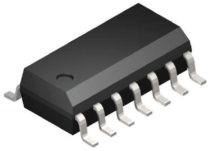
| 供应商器件封装 | 14-SOIC |
| 共模抑制比—最小值 | 65 dB |
| 关闭 | No Shutdown |
| 其它名称 | 296-22898-5 |
| 包装 | 管件 |
| 单位重量 | 130 mg |
| 单电源电压 | 8 V to 12 V |
| 压摆率 | 2500 V/µs |
| 双重电源电压 | +/- 5 V |
| 商标 | Texas Instruments |
| 增益带宽积 | - |
| 安装类型 | 表面贴装 |
| 安装风格 | SMD/SMT |
| 封装 | Tube |
| 封装/外壳 | 14-SOIC(0.154",3.90mm 宽) |
| 封装/箱体 | SOIC-14 |
| 工作温度 | -40°C ~ 85°C |
| 工作电源电压 | 8 V to 12 V |
| 工厂包装数量 | 50 |
| 技术 | BiCOM |
| 放大器类型 | 可变增益 |
| 最大双重电源电压 | +/- 6 V |
| 最大工作温度 | + 85 C |
| 最小双重电源电压 | +/- 4 V |
| 最小工作温度 | - 40 C |
| 标准包装 | 50 |
| 电压-电源,单/双 (±) | ±4 V ~ 6 V |
| 电压-输入失调 | 4mV |
| 电流-电源 | 36.5mA |
| 电流-输入偏置 | 19µA |
| 电流-输出/通道 | 90mA |
| 电路数 | 1 |
| 系列 | VCA824 |
| 转换速度 | 2500 V/us |
| 输入偏压电流—最大 | 25 uA |
| 输入补偿电压 | 17 mV |
| 输出类型 | - |
| 通道数量 | 1 Channel |
| 配用 | /product-detail/zh/DEM-VCA-SO-1B/296-30915-ND/1898362 |


- 商务部:美国ITC正式对集成电路等产品启动337调查
- 曝三星4nm工艺存在良率问题 高通将骁龙8 Gen1或转产台积电
- 太阳诱电将投资9.5亿元在常州建新厂生产MLCC 预计2023年完工
- 英特尔发布欧洲新工厂建设计划 深化IDM 2.0 战略
- 台积电先进制程称霸业界 有大客户加持明年业绩稳了
- 达到5530亿美元!SIA预计今年全球半导体销售额将创下新高
- 英特尔拟将自动驾驶子公司Mobileye上市 估值或超500亿美元
- 三星加码芯片和SET,合并消费电子和移动部门,撤换高东真等 CEO
- 三星电子宣布重大人事变动 还合并消费电子和移动部门
- 海关总署:前11个月进口集成电路产品价值2.52万亿元 增长14.8%


PDF Datasheet 数据手册内容提取
Product Order Technical Tools & Support & Folder Now Documents Software Community VCA824 SBOS394E–NOVEMBER2007–REVISEDJULY2019 VCA824 Ultra-Wideband, > 40-dB Gain Adjust Range, Linear in V/V Variable Gain Amplifier 1 Features The VCA824 internal architecture consists of two input buffers and an output current feedback amplifier • 710-MHzSmall-SignalBandwidth(G=2V/V) 1 stage integrated with a multiplier core to provide a • 320MHz,4-VPPBandwidth(G=10V/V) complete variable gain amplifier (VGA) system that • 0.1-dBGainFlatnessto135MHz does not require external buffering. The maximum gain is set externally with two resistors, providing • 2500-V/µsSlewRate flexibility in designs. The maximum gain is intended • >40-dBGainAdjustRange to be set between 2 V/V and 40 V/V. Operating from • HighGainAccuracy:20-dB±0.3-dB ±5-V supplies, the gain control voltage for the VCA824 adjusts the gain linearly in V/V as the control • HighOutputCurrent: ±90mA voltage varies from 1 V to –1 V. For example, set for a maximum gain of 10 V/V, the VCA824 provides 2 Applications 10 V/V, at 1-V input, to 0.1 V/V at –1-V input of gain • DifferentialLineReceivers control range. The VCA824 offers excellent gain • DifferentialEqualizers linearity. For a 20-dB maximum gain, and a gain- control input voltage varying between 0 V and 1 V, • PulseAmplitudeCompensation the gain does not deviate by more than ±0.3-dB • VariableAttenuators (maximumat25°C). • Voltage-TunableActiveFilters DeviceInformation(1) 3 Description PARTNUMBER PACKAGE BODYSIZE(NOM) The VCA824 is a DC-coupled, wideband, linear-in SOIC(14) 8.65mm×3.91mm VCA824 V/V, continuously variable, voltage-controlled gain VSSOP(10) 3.00mm×3.00mm amplifier. The device provides a differential input to (1) For all available packages, see the orderable addendum at single-ended conversion with a high-impedance gain theendofthedatasheet. control input used to vary the gain down 40 dB from the nominal maximum gain set by the gain resistor (R )andfeedbackresistor(R ). G F SPACE DifferentialEqualizationofanRCLoad DifferentialEqualizer 9 Equalized Frequency Response 6 R VIN1 +VIN F 3 R RG+ 0 Initial Frequency Response S RC11 RG R VCA824FB Gain (dB)-1---2369 of the VCA824 with RC Load G- VIN2 -VIN 20W --1158 RS -21 -24 1M 10M 100M 1G Frequency (Hz) 1 An IMPORTANT NOTICE at the end of this data sheet addresses availability, warranty, changes, use in safety-critical applications, intellectualpropertymattersandotherimportantdisclaimers.PRODUCTIONDATA.
VCA824 SBOS394E–NOVEMBER2007–REVISEDJULY2019 www.ti.com Table of Contents 1 Features.................................................................. 1 8.2 FunctionalBlockDiagram.......................................19 2 Applications........................................................... 1 8.3 FeatureDescription.................................................19 3 Description............................................................. 1 8.4 DeviceFunctionalModes........................................19 4 RevisionHistory..................................................... 2 9 ApplicationandImplementation........................ 22 9.1 ApplicationInformation............................................22 5 DeviceComparisonTable..................................... 3 9.2 TypicalApplication..................................................28 6 PinConfigurationandFunctions......................... 3 10 PowerSupplyRecommendations..................... 30 7 Specifications......................................................... 4 11 Layout................................................................... 30 7.1 AbsoluteMaximumRatings......................................4 11.1 LayoutGuidelines ................................................30 7.2 ESDRatings..............................................................4 11.2 LayoutExample....................................................31 7.3 RecommendedOperatingConditions.......................4 12 DeviceandDocumentationSupport................. 32 7.4 ThermalInformation..................................................4 7.5 ElectricalCharacteristics:V =±5V.........................5 12.1 DeviceSupport......................................................32 S 7.6 TypicalCharacteristics:V =±5V,A =2V/V...7 12.2 ReceivingNotificationofDocumentationUpdates32 S VMAX 7.7 TypicalCharacteristics:V =±5V,A =10 12.3 CommunityResources..........................................32 S VMAX V/V........................................................................... 11 12.4 Trademarks...........................................................32 7.8 TypicalCharacteristics:V =±5V,A =40 12.5 ElectrostaticDischargeCaution............................32 S VMAX V/V........................................................................... 15 12.6 Glossary................................................................32 8 DetailedDescription............................................ 19 13 Mechanical,Packaging,andOrderable 8.1 Overview.................................................................19 Information........................................................... 32 4 Revision History ChangesfromRevisionD(January2016)toRevisionE Page • ChangedOutputVoltageSwingparameterR =100Ωspecifications ................................................................................. 6 L • ChangedOutputCurrentparameterspecifications................................................................................................................ 6 ChangesfromRevisionC(December2008)toRevisionD Page • AddedPinConfigurationandFunctionssection,ESDRatingstable,FeatureDescriptionsection,DeviceFunctional Modes,ApplicationandImplementationsection,PowerSupplyRecommendationssection,Layoutsection,Device andDocumentationSupportsection,andMechanical,Packaging,andOrderableInformationsection............................... 1 • DeletedThermalCharacteristicsrowsfromElectricalCharacteristics .................................................................................. 5 ChangesfromRevisionB(August2008)toRevisionC Page • RevisedsecondparagraphintheWidebandVariableGainAmplifierOperationsectiondescribingpin9.......................... 28 ChangesfromRevisionA(December2007)toRevisionB Page • ChangedstoragetemperaturerangeratinginAbsoluteMaximumRatingstablefrom–40°Cto125°Cto–65°C to125°C .............................................................................................................................................................................. 4 ChangesfromOriginal(November2007)toRevisionA Page • Addedtypicalvalueforoutputimpedance............................................................................................................................. 6 • ChangedwordingofexplanationforX2Ycapacitorusageatendofparagraph.................................................................. 28 2 SubmitDocumentationFeedback Copyright©2007–2019,TexasInstrumentsIncorporated ProductFolderLinks:VCA824
VCA824 www.ti.com SBOS394E–NOVEMBER2007–REVISEDJULY2019 5 Device Comparison Table SINGLES DUALS GAINADJUSTRANGE(dB) INPUTNOISE(nV/√Hz) SIGNALBANDWIDTH(MHz) VCA810 — 80 2.4 35 — VCA2612 45 1.25 80 — VCA2613 45 1 80 — VCA2615 52 0.8 50 — VCA2617 48 4.1 50 VCA820 — 40 8.2 150 VCA821 — 40 6.0 420 VCA822 — 40 8.2 150 VCA824 — 40 6.0 420 6 Pin Configuration and Functions DPackage DGSPackage 14-PinSOIC 10-PinVSSOP TopView TopView +V 1 14 +V FB 1 10 GND CC CC V 2 13 NC +V 2 9 V G CC OUT +V 3 12 FB V 3 8 -V IN G CC +R 4 11 GND +V 4 7 -V G IN IN -R 5 10 V +R 5 6 -R G OUT G G -V 6 9 V IN REF -V 7 8 -V CC CC NC=NoConnection PinFunctions PIN I/O DESCRIPTION NAME SOIC VSSOP V 1,14 2 P Positivesupplyvoltage CC V 2 3 I Gaincontrolvoltage G +V 3 4 I noninvertinginput IN +R 4 5 I Gainsetresistornoninvertinginput G –R 5 6 I Gainsetresistorinvertinginput G –V 6 7 I Invertinginput IN –V 7,8 8 P Negativesupplyvoltage CC V 9 — I Outputreferencevoltage(Non-Invertinginputofoutputbuffer) REF V 10 9 O Outputvoltage OUT GND 11 10 P Ground FB 12 1 I Feedbackresistor(invertinginputofoutputbuffer) NC 13 — — Notconnected Copyright©2007–2019,TexasInstrumentsIncorporated SubmitDocumentationFeedback 3 ProductFolderLinks:VCA824
VCA824 SBOS394E–NOVEMBER2007–REVISEDJULY2019 www.ti.com 7 Specifications 7.1 Absolute Maximum Ratings overoperatingfree-airtemperaturerange(unlessotherwisenoted)(1) MIN MAX UNIT Powersupply ±6.5 V Internalpowerdissipation SeeThermalInformation Inputvoltage ±V V S Junctiontemperature(T) 260 °C J Junctiontemperature(T),continuousoperation 140 °C J Storagetemperature –65 125 °C (1) StressesbeyondthoselistedunderAbsoluteMaximumRatingsmaycausepermanentdamagetothedevice.Thesearestressratings only,whichdonotimplyfunctionaloperationofthedeviceattheseoranyotherconditionsbeyondthoseindicatedunderRecommended OperatingConditions.Exposuretoabsolute-maximum-ratedconditionsforextendedperiodsmayaffectdevicereliability. 7.2 ESD Ratings VALUE UNIT Humanbodymodel(HBM),perANSI/ESDA/JEDECJS-001(1) ±2000 Chargeddevicemodel(CDM),perJEDECspecificationJESD22- V(ESD) Electrostaticdischarge C101(2) ±500 V Machinemodel(MM) ±200 (1) JEDECdocumentJEP155statesthat500-VHBMallowssafemanufacturingwithastandardESDcontrolprocess. (2) JEDECdocumentJEP157statesthat250-VCDMallowssafemanufacturingwithastandardESDcontrolprocess. 7.3 Recommended Operating Conditions overoperatingfree-airtemperaturerange(unlessotherwisenoted) MIN NOM MAX UNIT Operatingvoltage 7 10 12 V Operatingtemperature –40 25 85 °C 7.4 Thermal Information VCA824 THERMALMETRIC(1) D(SOIC) DGS(VSSOP) UNIT 14PINS 10PINS R Junction-to-ambientthermalresistance 90.3 173.1 °C/W θJA R Junction-to-case(top)thermalresistance 49.8 46.6 °C/W θJC(top) R Junction-to-boardthermalresistance 44.9 94.3 °C/W θJB ψ Junction-to-topcharacterizationparameter 13.8 2.2 °C/W JT ψ Junction-to-boardcharacterizationparameter 44.6 92.7 °C/W JB R Junction-to-case(bottom)thermalresistance n/a n/a °C/W θJC(bot) (1) Formoreinformationabouttraditionalandnewthermalmetrics,seetheSemiconductorandICPackageThermalMetricsapplication report. 4 SubmitDocumentationFeedback Copyright©2007–2019,TexasInstrumentsIncorporated ProductFolderLinks:VCA824
VCA824 www.ti.com SBOS394E–NOVEMBER2007–REVISEDJULY2019 7.5 Electrical Characteristics: V = ±5 V S AtA =10V/V,V =1V,R =402Ω,R =80Ω,andR =100Ω,unlessotherwisenoted. VMAX G F G L PARAMETER TESTCONDITIONS TESTLEVEL(1) MIN TYP MAX UNIT ACPERFORMANCE AVMAX=2V/V,VG=1V,VO=500mVPP 710 Small-SignalBandwidth AVMAX=10V/V,VG=1V,VO=500mVPP C 420 MHz AVMAX=40V/V,VG=1V,VO=500mVPP 170 Large-SignalBandwidth AVMAX=10V/V,VG=1V,VO=4VPP C 320 MHz TA=25°C 240 330 GainControlBandwidth VO=200mVPP,TA=25°C TA=0°Cto70°C B 235 MHz TA=–40°Cto85°C 235 Bandwidthfor0.1-dBFlatness AVMAX=10V/V,VG=1V,VO=2VPP C 135 MHz TA=25°C 1800 2500 SlewRate A4VVMASXte=p10V/V,VG=1V,VO= TA=0°Cto70° B 1700 V/μs TA=–40°Cto85°C 1700 TA=25°C 1.5 1.8 Rise-and-FallTime A4VVMASXte=p10V/V,VG=1V,VO= TA=0°Cto70°C B 1.9 ns TA=–40°Cto85°C 1.9 SettlingTimeto0.01% AVMAX=10V/V,VG=1V,VO=4VStep C 11 ns TA=25°C –64 -66 2nd-Harmonic VO=2VPP,f=20MHz TA=0°Cto70°C B –64 dBc Harmonic TA=–40°Cto85°C –64 Distortion TA=25°C –61 –63 3rd-Harmonic VO=2VPP,f=20MHz TA=0°Cto70°C B –61 dBc TA=–40°Cto85°C –61 InputVoltageNoise f>100kHz C 6 nV/√Hz InputCurrentNoise f>100kHz C 2.6 pA/√Hz GAINCONTROL TA=25°C ±0.1 ±0.4 GainError AVMAX=10V/V,VG=1V TA=0°Cto70°C A ±0.5 dB TA=–40°Cto85°C ±0.6 TA=25°C ±0.05 ±0.3 GainDeviation AVMAX=10V/V,0<VG<1 TA=0°Cto70°C A ±0.34 dB TA=–40°Cto85°C ±0.37 TA=25°C ±1.06 ±1.9 GainDeviation AVMAX=10V/V,-0.8<VG<1 TA=0°Cto70°C A ±2.1 dB TA=–40°Cto85°C ±2.2 TA=25°C –26 –24 GainatVG=–0.9V Relativetomaxgain TA=0°Cto70°C A –24 dB TA=–40°Cto85°C –23 TA=25°C 22 30 GainControlBiasCurrent TA=0°Cto70°C A 35 μA TA=–40°Cto85°C 37 AverageGainControlBiasCurrent TA=0°Cto70°C B ±100 nA/°C Drift TA=–40°Cto85°C ±100 GainControlInputImpedance TA=25°C C 1.5||0.6 MΩ||pF DCPERFORMANCE TA=25°C ±4 ±17 InputOffsetVoltage AVVGM=AX1=V10V/V,VCM=0V, TA=0°Cto70° A ±17.8 mV TA=–40°Cto85°C ±19 AverageInputOffsetVoltageDrift AVMAX=10V/V,VCM=0V, TA=0°Cto70°C B ±30 μV/°C VG=1V TA=–40°Cto85°C ±30 TA=25°C 19 25 InputBiasCurrent AVVGM=AX1=V10V/V,VCM=0V, TA=0°Cto70°C A 29 μA TA=–40°Cto85°C 31 (1) Testlevels:(A)100%testedat25°C.Overtemperaturelimitssetbycharacterizationandsimulation.(B)Limitssetbycharacterization andsimulation.(C)Typicalvalueonlyforinformation. Copyright©2007–2019,TexasInstrumentsIncorporated SubmitDocumentationFeedback 5 ProductFolderLinks:VCA824
VCA824 SBOS394E–NOVEMBER2007–REVISEDJULY2019 www.ti.com Electrical Characteristics: V = ±5 V (continued) S AtA =10V/V,V =1V,R =402Ω,R =80Ω,andR =100Ω,unlessotherwisenoted. VMAX G F G L PARAMETER TESTCONDITIONS TESTLEVEL(1) MIN TYP MAX UNIT AverageInputBiasCurrentDrift AVMAX=10V/V,VCM=0V, TA=0°Cto70°C B ±90 nA/°C VG=1V TA=–40°Cto85° ±90 TA=25°C ±0.5 ±2.5 InputOffsetCurrent AVVGM=AX1=V10V/V,VCM=0V, TA=0°Cto70°C A ±3.2 μA TA=–40°Cto85°C ±3.5 AverageInputOffsetCurrentDrift AVMAX=10V/V,VCM=0V, TA=0°Cto70°C B ±16 nA/°C VG=1V TA=–40°Cto85°C ±16 TA=25°C ±2.6 ±2.55 MaxCurrentThroughGainResistance TA=0°Cto70°C B ±2.55 mA TA=–40°Cto85°C ±2.5 INPUT TA=25°C 1.6 1.6 MostPositiveCommon-ModeInput Voltage RL=100Ω TA=0°Cto70°C A 1.6 V TA=–40°Cto85°C 1.6 TA=25°C –2.1 –2.1 MostNegativeCommon-ModeInput Voltage RL=100Ω TA=0°Cto70°C A –2.1 V TA=–40°Cto85°C –2.1 TA=25°C 80 65 Common-ModeRejectionRatio VCM=±0.5V TA=0°Cto70°C A 60 dB TA=–40°Cto85°C 60 Differential C 1||1 MΩ||pF InputImpedance Common-Mode C 1||2 MΩ||pF OUTPUT TA=25°C ±3.6 ±3.9 RL=1kΩ TA=0°Cto70°C A ±3.4 V TA=–40°Cto85°C ±3.3 OutputVoltageSwing 3.5 3.6 TA=25°C –3.3 –3.2 RL=100Ω TA=0°Cto70°C A 3.3 –3 V TA=–40°Cto85°C 3.2 –2.9 Source,TA=25°C 60 90 OutputCurrent VO=0V,RL=10Ω STAin=k,0T°AC=to257°0C°C A 50 –55 ––5402 mA TA=–40°Cto85°C 45 –38 OutputImpedance AVMAX=10V/V,f>100kHz C 0.01 Ω POWERSUPPLY SpecifiedOperatingVoltage C ±5 V TA=25°C ±4 MinimumOperatingVoltage TA=0°Cto70°C B ±4 V TA=–40°Cto85°C ±4 TA=25°C ±6 MaximumOperatingVoltage TA=0°Cto70°C A ±6 V TA=–40°Cto85°C ±6 TA=25°C 36.5 37.5 MaximumQuiescentCurrent VG=0V TA=0°Cto70°C A 38 mA TA=–40°Cto85°C 38.5 TA=25°C 36.5 35 MinimumQuiescentCurrent VG=0V TA=0°Cto70°C A 34.5 mA TA=–40°Cto85°C 34 TA=25°C –61 -68 Power-SupplyRejectionRatio (-PSRR) VG=1V TA=0°Cto70°C A –59 dB TA=–40°Cto85°C –58 6 SubmitDocumentationFeedback Copyright©2007–2019,TexasInstrumentsIncorporated ProductFolderLinks:VCA824
VCA824 www.ti.com SBOS394E–NOVEMBER2007–REVISEDJULY2019 7.6 Typical Characteristics: V = ±5 V, A = 2 V/V S VMAX AtT =25°C,R =100Ω,R =453Ω,R =453Ω,V =1V,V =single-endedinputon+V with–V atground,and14- A L F G G IN IN IN PinSOICpackage,unlessotherwisenoted. 3 3 VG= 0V VO= 0.5VPP 0 0 B) -3 B) -3 d d ain ( -6 VG= +1V ain ( -6 VO= 1VPP G G d d VO= 2VPP ze -9 ze -9 mali mali VO= 4VPP or -12 or -12 N N V = 5V A = +2V/V O PP -15 VVM=AX 1V -15 IN PP R = 100W -18 L -18 1M 10M 100M 1G 1M 10M 100M 1G Frequency (Hz) Frequency (Hz) Figure1.Small-SignalFrequencyResponse Figure2.Large-SignalFrequencyResponse 400 4 VIN= 250mVPP VIN= 2VPP 300 f = 20MHz 3 f = 20MHz Output Voltage (mV) -2110000000 Output Voltage (V) -2101 -200 -2 -300 -3 Time (10ns/div) Time (10ns/div) Figure3.Small-SignalPulseResponse Figure4.Large-SignalPulseResponse 0 0 0.2 0.15 -0.1 -0.005 Left Scale Differential Gain (%) ------000000......234567 -dP, VG= 0V -dG, V-Gd=P, 0VVG= +1V ------000000......000000112233050505 Differential Phase ()°Magnitude (dB) ---0000....10123 Right Scale 000--00..10..010550 Deviation from Linear Phase -0.8 -0.040 -0.4 AVMAX= +2V/V -0.15 ()° -0.9 -dG, VG= +1V -0.045 -0.5 VG= +1V -0.20 1 2 3 4 0 50 100 150 200 Number of Video Loads Frequency (MHz) Figure5.CompositeVideodG/dP Figure6.GainFlatness,DeviationFromLinearPhase Copyright©2007–2019,TexasInstrumentsIncorporated SubmitDocumentationFeedback 7 ProductFolderLinks:VCA824
VCA824 SBOS394E–NOVEMBER2007–REVISEDJULY2019 www.ti.com Typical Characteristics: V = ±5 V, A = 2 V/V (continued) S VMAX AtT =25°C,R =100Ω,R =453Ω,R =453Ω,V =1V,V =single-endedinputon+V with–V atground,and14- A L F G G IN IN IN PinSOICpackage,unlessotherwisenoted. -60 -60 A = +2V/V VMAX -65 -65 VG= +1V c) c) VO= 2VPP on (dB -70 3rd-Harmonic on (dB -70 f = 20MHz 2nd-Harmonic storti -75 storti -75 Di Di c c oni -80 oni -80 m A = +2V/V m 3rd-Harmonic Har -85 2nd-Harmonic VMAXVG= +1V Har -85 V = 2V O PP R = 100W -90 L -90 0.1 1 10 100 100 1k Frequency (MHz) Resistance (W) Figure7.HarmoneicDistortionvsFrequency Figure8.HarmonicDistortionvsLoadResistance -30 -10 Distortion (dBc) ------344556505050 AVRf =VGL M=2=A0 X1+M01=H0V +Wz2V/V TMhraoxuimghu mRG CLuirmreitnetd Distortion (dBc) ----23450000 TMhraoxuimghu3 mRrdG C-HLuiarmrremitneotdnic AVMARfVX =LO= =2= + 0 122M0VV0HP/WVzP Harmonic ---677505 2nd-Harmonic Harmonic --6700 2nd-Harmonic -80 3rd-Harmonic -80 -85 -90 0.1 1 10 -0.6 -0.4 -0.2 0 0.2 0.4 0.6 0.8 1.0 Output Voltage Swing (V ) Gain Control Voltage (V) PP Figure9.HarmonicDistortionvsOutputVoltage Figure10.HarmonicDistortionvsGainControlVoltage 38 40 f = 20MHz Constant Input Voltage At 50WMatched Load 36 35 m) m) Constant Output Voltage B 34 B d d 30 + + nt ( 32 nt ( oi oi 25 P P pt 30 pt e e nterc 28 nterc 20 I I 26 15 At 50WMatched Load 24 10 0 10 20 30 40 50 60 70 80 90 100 -0.6 -0.4 -0.2 0 0.2 0.4 0.6 0.8 1.0 Frequency (MHz) Gain Control Voltage (V) Figure11.Two-Tone,3rd-OrderIntermodulationIntercept Figure12.Two-Tone,3rd-OrderIntermodulationInterceptvs GainControlVoltage 8 SubmitDocumentationFeedback Copyright©2007–2019,TexasInstrumentsIncorporated ProductFolderLinks:VCA824
VCA824 www.ti.com SBOS394E–NOVEMBER2007–REVISEDJULY2019 Typical Characteristics: V = ±5 V, A = 2 V/V (continued) S VMAX AtT =25°C,R =100Ω,R =453Ω,R =453Ω,V =1V,V =single-endedinputon+V with–V atground,and14- A L F G G IN IN IN PinSOICpackage,unlessotherwisenoted. 2.2 3 2.0 VG= 0VDC+ 10mVPP V = 0.5V 1.8 IN DC 0 1.6 B) 1.4 d V/V) 1.2 Gain ( -3 Gain ( 10..08 alized -6 0.6 m 0.4 Nor 0.2 -9 0 -0.2 -12 -1.2 -0.8 -0.4 0 0.4 0.8 1.2 1M 10M 100M 1G Gain Control Voltage (V) Frequency (Hz) Figure13.GainvsGainControlVoltage Figure14.GainControlFrequencyResponse 4 10 V = 1V O IN DC 3 utpu -100 VG= +1V 2 t Vo -20 1 ltag -30 e (V) 11..50 0-1e (V) Gain (dB) ---456000 VG=-1V ag 0.5 -70 Volt 0 -80 put -0.5 -90 VG= 2VPP In -100 -1.0 1M 10M 100M 1G Time (10ns/div) Frequency (Hz) Figure15.GainControlPulseResponse Figure16.Fully-AttenuatedResponse 2.0 1.6 1.8 10MHz 1.4 1.6 1.2 s) 1.4 s) n n y ( 1.2 y ( 1.0 a a p Del 1.0 1MHz p Del 0.8 ou 0.8 20MHz ou 0.6 Gr 0.6 Gr 0.4 0.4 V = +1V 0.2 0.2 VG= 1V O PP 0 0 -1.0 -0.8 -0.6 -0.4 -0.2 0 0.2 0.4 0.6 0.8 1.0 0 20 40 60 80 100 Gain Control Voltage (V) Frequency (MHz) Figure17.GroupDelayvsGainControlVoltage Figure18.GroupDelayvsFrequency Copyright©2007–2019,TexasInstrumentsIncorporated SubmitDocumentationFeedback 9 ProductFolderLinks:VCA824
VCA824 SBOS394E–NOVEMBER2007–REVISEDJULY2019 www.ti.com Typical Characteristics: V = ±5 V, A = 2 V/V (continued) S VMAX AtT =25°C,R =100Ω,R =453Ω,R =453Ω,V =1V,V =single-endedinputon+V with–V atground,and14- A L F G G IN IN IN PinSOICpackage,unlessotherwisenoted. 100 9 VO= 0.5VPP CL= 10pF 6 CL= 100pF CL= 22pF 3 W) W) CL= 47pF R(S 10 R(S 0 -3 VIN + RF VCA824 RS VOUT -6 - CL 1kW(1) 0.1dB Flatness Targeted NOTE: (1) 1kWis optional. 1 -9 1 10 100 1k 1 10 100 1k Capacitive Load (pF) Capacitive Load (pF) Figure19.RecommendedR vsCapacitiveLoad Figure20.FrequencyResponsevsCapacitiveLoad S 200 10 )Hz )z Öensity (nV/ 100 VG= 0VVG= +1V Önsity (pA/H D e se e D Noi ois ge e N a g Volt olta put VG=-1V ut V Out Inp 10 1 100 1k 10k 100k 1M 10M 100 1k 10k 100k 1M 10M Frequency (Hz) Frequency (Hz) Figure21.OutputVoltageDensity Figure22.InputCurrentNoiseDensity 10 SubmitDocumentationFeedback Copyright©2007–2019,TexasInstrumentsIncorporated ProductFolderLinks:VCA824
VCA824 www.ti.com SBOS394E–NOVEMBER2007–REVISEDJULY2019 7.7 Typical Characteristics: V = ±5 V, A = 10 V/V S VMAX AtT =25°C,R =100Ω,R =402Ω,R =80Ω,V =1V,andV =single-endedinputon+V with–V atground,unless A L F G G IN IN IN otherwisenoted. 3 3 V = 0V 0 G 0 V = 1V O PP B) -3 B) -3 n (d n (d VO= 0.5VPP ai -6 ai -6 G G zed -9 VG= +1V zed -9 ali ali m m or -12 or -12 N N -15 AVVM=AX 2=0 0+m10VV/V -15 VO= 4VPP RIN= 100W PP VO= 2VPP -18 G -18 1M 10M 100M 1G 0 200M 400M 600M 800M 1G Frequency (Hz) Frequency (Hz) Figure23.Small-SignalFrequencyResponse Figure24.Large-SignalFrequencyResponse 300 3 VINf= = 5 200mMVHPzP VIN=f 4=0 200mMVHPzP 200 2 Output Voltage (mV) -1100000 Output Voltage (V) -101 -200 -2 -300 -3 Time (10ns/div) Time (10ns/div) Figure25.Small-SignalPulseResponse Figure26.Large-SignalPulseResponse 0.1 0.20 200 )z H Magnitude (dB) ----0000....01234 Right Scale Left Scale 0000-0...110.05055 Deviation from Linear Phas ÖVoltage Noise Density (nV/ 100 VG= 0V VG= +1V VG=-1V --00..56 AVVGM=A X+1=V +10V/V --00..1105 e ()° Output 10 0 50 100 150 200 100 1k 10k 100k 1M 10M Frequency (MHz) Frequency (Hz) Figure27.GainFlatness,DeviationfromLinearPhase Figure28.OutputVoltageNoiseDensity Copyright©2007–2019,TexasInstrumentsIncorporated SubmitDocumentationFeedback 11 ProductFolderLinks:VCA824
VCA824 SBOS394E–NOVEMBER2007–REVISEDJULY2019 www.ti.com Typical Characteristics: V = ±5 V, A = 10 V/V (continued) S VMAX AtT =25°C,R =100Ω,R =402Ω,R =80Ω,V =1V,andV =single-endedinputon+V with–V atground,unless A L F G G IN IN IN otherwisenoted. -50 -66 A = +10V/V VMAX -55 -68 VG= +1V V = 1V c) c) O PP dB -60 dB -70 f = 20MHz ortion ( -65 3rd-Harmonic ortion ( -72 c Dist -70 c Dist -74 3rd-Harmonic ni ni mo -75 A = +10V/V mo -76 Har -80 2nd-Harmonic VMAXVVG== 2 +V1V Har -78 O PP R = 100W 2nd-Harmonic -85 L -80 0.1 1 10 100 100 1k Frequency (MHz) Resistance (W) Figure29.HarmonicDistortionvsFrequency Figure30.HarmonicDistortionvsLoadResistance -20 -10 A = +10V/V A = +10V/V VMAX VMAX monic Distortion (dBc) -----3456700000 VRf =GL =2=0 1+M01H0VWz 2nd-HarmoniTcMhraoxuimghu mRG CLuirmreitnetd monic Distortion (dBc) ----23450000 TMhra3oxrudimg-hHu amRrG mCLouinrmriceitnetd RfV =LO =2= 0 12M0V0HPWzP Har -80 3rd-Harmonic Har -60 2nd-Harmonic -90 -70 0.1 1 10 -0.6 -0.4 -0.2 0 0.2 0.4 0.6 0.8 1.0 Output Voltage Swing (V ) Gain Control Voltage (V) PP Figure31.HarmonicDistortionvsOutputVoltage Figure32.HarmonicDistortionvsGainControlVoltage 34 35 Constant Input Voltage 32 30 m) m) B B Constant Output Voltage d d + + nt ( 30 nt ( 25 oi oi P P ept 28 ept 20 c c er er nt nt I 26 I 15 f = 20MHz At 50WMatched Load At 50WMatched Load 24 10 0 10 20 30 40 50 60 70 80 90 100 -0.6 -0.4 -0.2 0 0.2 0.4 0.6 0.8 1.0 Frequency (MHz) Gain Control Voltage (V) Figure33.Two-Tone,3rd-OrderIntermodulationIntercept Figure34.Two-Tone,3rd-OrderIntermodulationInterceptvs GainControlVoltage 12 SubmitDocumentationFeedback Copyright©2007–2019,TexasInstrumentsIncorporated ProductFolderLinks:VCA824
VCA824 www.ti.com SBOS394E–NOVEMBER2007–REVISEDJULY2019 Typical Characteristics: V = ±5 V, A = 10 V/V (continued) S VMAX AtT =25°C,R =100Ω,R =402Ω,R =80Ω,V =1V,andV =single-endedinputon+V with–V atground,unless A L F G G IN IN IN otherwisenoted. 11 3 V = 0V + 10mV 10 G DC PP V = 0.1V 9 0 IN DC 8 B) V/V) 76 Gain (d -3 ain ( 54 zed -6 G ali 3 m -9 2 Nor 1 -12 0 -1 -15 -1.2 -0.8 -0.4 0 0.4 0.8 1.2 1M 10M 100M 1G Gain Control Voltage (V) Frequency (Hz) Figure35.GainvsGainControlVoltage Figure36.GainControlFrequencyResponse 3 5 VIN= 0.2VDC 2 Outp 4 1PWow Ienrternal 1 ut Vo 3 Dissipation 1L0o0aWd age (V) 110...505 0-1ltage (V) Output Voltage (V) --21012 L5o0aWd L2o5aWd Volt 0 -3 1W Internal ut -4 Power np -0.5 Dissipation I -5 -1.0 -150 -100 -50 0 50 100 150 Time (10ns/div) Output Current (mA) Figure37.GainControlPulseResponse Figure38.OutputVoltageandCurrentLimitations 30 0.4 2.0 A = +10V/V 20 Input Voltage VMAX 10 VG= +1V 0.3 Left Scale VG=-0.3V 1.5 0 0.2 1.0 -10 V) Ou Gain (dB) -----2345600000 VG=-1V Input Voltage ( -00..101 ORiugthptu St cVaolletage 00-0.5.5 tput Voltage (V -70 -0.2 -1.0 ) -80 Input Referred -90 VO= 2VPP -0.3 -1.5 -100 -0.4 -2.0 1M 10M 100M 1G Time (40ns/div) Frequency (Hz) Figure40.I LimitedOverdriveRecovery RG Figure39.Fully-AttenuatedResponse Copyright©2007–2019,TexasInstrumentsIncorporated SubmitDocumentationFeedback 13 ProductFolderLinks:VCA824
VCA824 SBOS394E–NOVEMBER2007–REVISEDJULY2019 www.ti.com Typical Characteristics: V = ±5 V, A = 10 V/V (continued) S VMAX AtT =25°C,R =100Ω,R =402Ω,R =80Ω,V =1V,andV =single-endedinputon+V with–V atground,unless A L F G G IN IN IN otherwisenoted. 0.6 6 1.65 A = +10V/V VMAX V = +1V 10MHz 0.4 Output Voltage G 4 1.60 Input Voltage (V) -00..202 Right Scale 20-2 Output Voltage (V) Group Delay (ns) 111...554505 1MHz 20MHz -0.4 Input Voltage -4 Left Scale 1.40 -1.0 -0.8 -0.6 -0.4 -0.2 0 0.2 0.4 0.6 0.8 1.0 -0.6 -6 Gain Control Voltage (V) Time (40ns/div) Figure42.GroupDelayvsGainControlVoltage Figure41.OutputLimitedOverdriveRecovery 1.8 1.6 1.4 ns) 1.2 y ( a 1.0 el D p 0.8 u o Gr 0.6 0.4 V = +1V 0.2 G V = 1V O PP 0 0 20 40 60 80 100 Frequency (MHz) Figure43.GroupDelayvsFrequency 14 SubmitDocumentationFeedback Copyright©2007–2019,TexasInstrumentsIncorporated ProductFolderLinks:VCA824
VCA824 www.ti.com SBOS394E–NOVEMBER2007–REVISEDJULY2019 7.8 Typical Characteristics: V = ±5 V, A = 40 V/V S VMAX AtT =25°C,R =100Ω,R =402Ω,R =18Ω,V =1V,V =single-endedinputon+V with–V atground,andSO-14 A L F G G IN IN IN package,unlessotherwisenoted. 3 3 0 0 V = 0V B) -3 G B) -3 d d n ( n ( VO= 4VPP VO= 0.5VPP ai -6 ai -6 G G zed -9 VG= +1V zed -9 VO= 1VPP ali ali m m or -12 or -12 N N V = 2V A = +40V/V O PP -15 VVM=AX 50mV -15 IN PP R = 100W -18 L -18 1M 10M 100M 1G 0 100 200 200 400 500 600 Frequency (Hz) Frequency (MHz) Figure44.Small-SignalFrequencyResponse Figure45.Large-SignalFrequencyResponse 400 2.5 300 VIN= f1 =2 .250mMVHPzP 2.0 VIN=f 1=0 200mMVHPzP 1.5 Output Voltage (mV) -2110000000 Output Voltage (V) --1001....05050 -1.5 -200 -2.0 -300 -2.5 Time (10ns/div) Time (10ns/div) Figure46.Small-SignalPulseResponse Figure47.Large-SignalPulseResponse 0.2 0.15 1000 AVMAX= +40V/V Hz) Magnitude (dB) ----00000.....101234 VG= +1V 000---000..10...01105505 Deviation from Linear Phase ()° Öutput Voltage Noise Density (nV/ 100 VVVGGG===- +011VVV O -0.5 -0.20 10 0 20 40 60 200 100 1k 10k 100k 1M 10M Frequency (MHz) Frequency (Hz) Figure48.GainFlatness,DeviationfromLinearPhase Figure49.OutputVoltageNoiseDensity Copyright©2007–2019,TexasInstrumentsIncorporated SubmitDocumentationFeedback 15 ProductFolderLinks:VCA824
VCA824 SBOS394E–NOVEMBER2007–REVISEDJULY2019 www.ti.com Typical Characteristics: V = ±5 V, A = 40 V/V (continued) S VMAX AtT =25°C,R =100Ω,R =402Ω,R =18Ω,V =1V,V =single-endedinputon+V with–V atground,andSO-14 A L F G G IN IN IN package,unlessotherwisenoted. -35 -50 A = +40V/V VMAX -40 VG= +1V -55 dBc) -45 VROL== 120V0PWP dBc) -60 ortion ( -50 ortion ( -65 3rd-Harmonic st st c Di -55 c Di -70 ni ni mo -60 mo -75 Har -65 2nd-Harmonic Har -80 AVVGM=A X+1=V +40V/V 2nd-Harmonic V = 1V -70 3rd-Harmonic -85 f =O 20MHPPz 0.1 1 10 100 100 1k Frequency (MHz) Resistance (W) Figure50.HarmonicDistortionvsFrequency Figure51.HarmonicDistortionvsLoadResistance -10 -10 A = +40V/V A = +40V/V VMAX VMAX -20 VG= +1V -15 VO= 2VPP monic Distortion (dBc) ----34560000 Rf =L =20 1M0H0Wz2nd-Harmonic TMhraoxuimghu mRG CLuirmreitnetd monic Distortion (dBc) -----2233405050 2nd-Harmonic TMhraoxuimghu3 mRrdG -CHLuairmrrmeitneotdnic Rf =L =2 01M00HWz Har 3rd-Harmonic Har -45 -70 -50 -80 -55 0.1 1 10 -0.6 -0.4 -0.2 0 0.2 0.4 0.6 0.8 1.0 Output Voltage Swing (V ) Gain Control Voltage (V) PP Figure52.HarmonicDistortionvsOutputVoltage Figure53.HarmonicDistortionvsGainControlVoltage 34 35 32 30 Bm) Bm) Constant Input Voltage d 30 d oint (+ 28 oint (+ 25 Constant Output Voltage P P pt pt 20 e e erc 26 erc nt nt I I 15 24 f = 20MHz At 50WMatched Load At 50WMatched Load 22 10 0 10 20 30 40 50 60 70 80 90 100 -0.6 -0.4 -0.2 0 0.2 0.4 0.6 0.8 1.0 Frequency (MHz) Gain Control Voltage (V) Figure54.Two-Tone,3rd-OrderIntermodulationIntercept Figure55.Two-Tone,3rd-OrderIntermodulationInterceptvs GainControlVoltage 16 SubmitDocumentationFeedback Copyright©2007–2019,TexasInstrumentsIncorporated ProductFolderLinks:VCA824
VCA824 www.ti.com SBOS394E–NOVEMBER2007–REVISEDJULY2019 Typical Characteristics: V = ±5 V, A = 40 V/V (continued) S VMAX AtT =25°C,R =100Ω,R =402Ω,R =18Ω,V =1V,V =single-endedinputon+V with–V atground,andSO-14 A L F G G IN IN IN package,unlessotherwisenoted. 45 3 40 0 35 Intercept Point (+dBm) 32211050505 Normalized Gain (dB)-1---2369 0 -15 VG= 0VDC+ 10mVPP V = 10mV -5 -18 IN DC -1.2 -0.8 -0.4 0 0.4 0.8 1.2 1M 10M 100M 1G Gain Control Voltage (V) Frequency (Hz) Figure56.GainvsGainControlVoltage Figure57.GainControlFrequencyResponse 3 V) 40 VIN= 50mVDC 2 ge ( 30 V = +1V 1 olta 20 G V 10 0 put 0 -1Out dB) -10 e (V) 11..50 Gain ( ---234000 ag 0.5 -50 VG=-1V Volt 0 -60 Input Referred put -0.5 -70 VO= 2VPP In -80 -1.0 1M 10M 100M 1G Time (10ns/div) Frequency (Hz) Figure58.GainControlPulseResponse Figure59.FullyAttenuatedResponse 0.4 1.6 0.3 6 A = +40V/V A = +40V/V Input Voltage VMAX VMAX 0.3 Left Scale VG=-0.3V 1.2 0.2 Output Voltage VG= +1V 4 Right Scale 0.2 0.8 Input Voltage (V) --000...1012 00--00.4..48 Output Voltage (V) Input Voltage (V) -00..101 20-2 Output Voltage (V) Input Voltage Output Voltage -0.2 -4 -0.3 Right Scale -1.2 Left Scale -0.4 -1.6 -0.3 -6 Time (40ns/div) Time (40ns/div) Figure60.I LimitedOverdriveRecovery Figure61.OutputLimitedOverdriveRecovery RG Copyright©2007–2019,TexasInstrumentsIncorporated SubmitDocumentationFeedback 17 ProductFolderLinks:VCA824
VCA824 SBOS394E–NOVEMBER2007–REVISEDJULY2019 www.ti.com Typical Characteristics: V = ±5 V, A = 40 V/V (continued) S VMAX AtT =25°C,R =100Ω,R =402Ω,R =18Ω,V =1V,V =single-endedinputon+V with–V atground,andSO-14 A L F G G IN IN IN package,unlessotherwisenoted. 2.15 2.5 10MHz 2.10 20MHz 2.0 2.05 s) s) n n Delay ( 2.00 1MHz Delay ( 1.5 Group 11..9950 Group 1.0 1.85 0.5 V = +1V G V = 1V 1.80 O PP -1.0 -0.8 -0.6 -0.4 -0.2 0 0.2 0.4 0.6 0.8 1.0 0 0 20 40 60 80 100 Gain Control Voltage (V) Frequency (MHz) Figure62.GroupDelayvsGainControlVoltage Figure63.GroupDelayvsFrequency 18 SubmitDocumentationFeedback Copyright©2007–2019,TexasInstrumentsIncorporated ProductFolderLinks:VCA824
VCA824 www.ti.com SBOS394E–NOVEMBER2007–REVISEDJULY2019 8 Detailed Description 8.1 Overview The VCA824 is a voltage controlled variable gain amplifier with differential inputs and a single ended output. The maximum gain is set by external resistors while the gain range is controlled by an external analog voltage. The maximum gain is designed for gains of 2 V/V up to 100 V/V and the analog control allows a gain range of over 40 dB. The VCA824 Input consists of two buffers, which together create a fully symmetrical, high impedance differential input with a typical common mode rejection of 80 dB. The gain set resistor is connected between the two input buffer output pins, so that the input impedance is independent of the gain settings. The bipolar inputs have a input voltage range of 1.6 and –2.1 V on ±5 V supplies. The amplifier maximum gain is set by external resistors, but the internal gain control circuit is controlled by a continuously variable, analog voltage. The gain control is a multiplier stage which is linear in V/V. The gain control input pin operates over a voltage range of –1 V to 1 V. The VCA824 contains a high-speed, high-current output buffer. The output stage can typically swing ±3.9Vandsource/sink ±90mA.TheVCA824canbeoperatedoveravoltagerangeof ±3.5Vto ±6V. 8.2 Functional Block Diagram +V V IN R IN F R 50W 1 RG+ Source 50W R V G OUT R G- 50W R Load 3 -V R IN 2 50W V G 8.3 Feature Description The VCA824 can be operated with both single ended or differential input signals. The inputs present consistently high impedance across all gain configurations. By using an analog control signal the amplifier gain is continuously variable for smooth, glitch free gain changes. With a large signal bandwidth of 320 Mhz and a slew rate of 2500 V/us the VCA824 offers linear performance over a wide range of signal amplitudes and gain settings. The low impedance/high current output buffer can drive loads ranging from low impedance transmission lines to high-impedance, switched-capacitor analog-to-digital converters. By using closely matched internal components,theVCA824offersgainaccuracyof ±0.3dB. 8.4 Device Functional Modes The VCA824 functions as a differential input, single maximum gain of operation-ended output variable gain amplifier. This functional mode is enabled by applying power to the amplifier supply pins and is disabled by turning the power off. The gain is continuously variable through the analog gain control input. While the gain range is fixed, the maximum gain is set by two external components, Rf and Rg, as shown in the Functional Block Diagram. The maximum gain is equal to 2x (Rf / Rg). This gain is achieved with a 1-V voltage on the gain adjust pin VG. As the voltage decreases on the VG pin, the gain decreases in a linear in dB fashion with over 40 dB of gain range from 1-V to –1-V control voltage. As with most other differential input amplifiers, inputs can be applied to either one or both of the amplifier inputs. The amplifier gain is controlled through the gain control pin. 8.4.1 MaximumGainOfOperation This section describes the use of the VCA824 in a fixed-gain application in which the V control pin is set at G V =1V.Thetradeoffsdescribedherearewithbandwidth,gain,andoutputvoltagerange. G Copyright©2007–2019,TexasInstrumentsIncorporated SubmitDocumentationFeedback 19 ProductFolderLinks:VCA824
VCA824 SBOS394E–NOVEMBER2007–REVISEDJULY2019 www.ti.com Device Functional Modes (continued) In the case of an application that does not make use of the V , but requires some other characteristic of the GAIN VCA824, the R resistor must be set such that the maximum current flowing through the resistance I is less G RG than±2.6mAtypical,or5.2mA asdefinedinElectricalCharacteristics:V =±5V,andmustfollowEquation1. PP S V OUT I = RG A ´R VMAX G (1) As Equation 1 illustrates, once the output dynamic range and maximum gain are defined, the gain resistor is set. This gain setting in turn affects the bandwidth, because in order to achieve the gain (and with a set gain element), the feedback element of the output stage amplifier is set as well. Keeping in mind that the output amplifieroftheVCA824isacurrent-feedbackamplifier,the larger the feedback element, the lower the bandwidth becausethefeedbackresistoristhecompensationelement. Limiting the discussion to the input voltage only and ignoring the output voltage and gain, Equation 2 illustrates thetradeoffbetweentheinputvoltageandthecurrentflowingthroughthegainresistor. 8.4.2 OutputCurrentAndVoltage The VCA824 provides output voltage and current capabilities that are unsurpassed in a low-cost monolithic VCA. Under no-load conditions at 25°C, the output voltage typically swings closer than 1 V to either supply rails; the 25°C swing limit is within 1.2 V of either rails. Into a 15-Ω load (the minimum tested load), the VCA824 device is testedtodelivermorethan±160mA. The specifications described above, though familiar in the industry, consider voltage and current limits separately. In many applications, it is the voltage × current, or V-I product, that is more relevant to circuit operation (See Figure 38). The X- and Y-axes of this graph show the zero-voltage output current limit and the zero-current output voltage limit, respectively. The four quadrants give a more detailed view of the VCA824 output drive capabilities, noting that the graph is bounded by a Safe Operating Area of 1-W maximum internal power dissipation. Superimposing resistor load lines onto the plot shows that the VCA824 can drive ±2.5 V into 25-Ω or ±3.5 V into 50-Ω without exceeding the output capabilities or the 1-W dissipation limit. A 100-Ω load line (thestandardtestcircuitload)showsthefull ±3.9-Voutputswingcapability,asshowninTypicalCharacteristics. The minimum specified output voltage and current overtemperature are set by worst-case simulations at the cold temperature extreme. Only at cold startup do the output current and voltage decrease to the numbers shown in Electrical Characteristic. As the output transistors deliver power, the respective junction temperatures increase, therebyincreasingtheavailableoutputvoltageswingandoutputcurrent. In steady-state operation, the available output voltage and current are always greater than the temperature shown in the overtemperature specifications because the output stage junction temperatures are higher than the specifiedoperatingambient. 8.4.3 InputVoltageDynamicRange The VCA824 has a input dynamic range limited to 1.6 V and –2.1 V. Increasing the input voltage dynamic range can be done by using an attenuator network on the input. If the VCA824 is trying to regulate the amplitude at the output,suchasinanAGCapplication,theinputvoltagedynamicrangeisdirectlyproportionaltoEquation2. V = R ´I IN(PP) G RG(PP) (2) As such, for unity-gain or under-attenuated conditions, the input voltage must be limited to the CMIR of ±1.6 V (3.2 V ) and the current (I ) must flow through the gain resistor, ±2.6 mA (5.2 mA ). This configuration sets a PP RQ PP minimumvalueforR suchthatthegainresistormustbegreaterthanEquation3. E 3.2V R = PP = 615.4W GMIN 5.2mA PP (3) Values lower than 615.4 Ω are gain elements that result in reduced input range, as the dynamic input range is limited by the current flowing through the gain resistor R (I ). If the I current limits the performance of the G RG RG circuit, the input stage of the VCA824 goes into overdrive, resulting in limited output voltage range. Such I - RG limitedoverdriveconditionsareshowninFigure40forthegainof10V/VandFigure60 forthegainof40V/V. 20 SubmitDocumentationFeedback Copyright©2007–2019,TexasInstrumentsIncorporated ProductFolderLinks:VCA824
VCA824 www.ti.com SBOS394E–NOVEMBER2007–REVISEDJULY2019 Device Functional Modes (continued) 8.4.4 OutputVoltageDynamicRange With its large output current capability and its wide output voltage swing of ±3.9 V typical on 100-Ω load, it is easy to forget other types of limitations that the VCA824 can encounter. For these limitations, careful analysis must be done to avoid input stage limitation: either voltage or I current. Note that if control pin V varies, the RG G gainlimitationmayaffectotheraspectsofthecircuit. 8.4.5 Bandwidth The output stage of the VCA824 is a wideband current-feedback amplifier. As such, the feedback resistance is the compensation of the last stage. Reducing the feedback element and maintaining the gain constant limits the useful range of I , and therefore, reduces the gain adjust range. For a given gain, reducing the gain element RG limitsthemaximumachievableoutputvoltageswing. 8.4.6 OffsetAdjustment As a result of the internal architecture used on the VCA824, the output offset voltage originates from the output stage and from the input stage and multiplier core. Figure 67 shows how to compensate both sources of the output offset voltage. Use this procedure to compensate the output offset voltage: starting with the output stage compensation, set V = –1 V to eliminate all offset contribution of the input stage and multiplier core. Adjust the G output stage offset compensation potentiometer. Finally, set V = 1 V to the maximum gain and adjust the input G stage and multiplier core potentiometer. This procedure effectively eliminates all offset contribution at the maximum gain. Because adjusting the gain modifies the contribution of the input stage and the multiplier core, someresidualoutputoffsetvoltageremains. 8.4.7 Noise The VCA824 offers 6 nV/√Hz input-referred voltage noise density at a gain of 10 V/V and 2.6-pA/√Hz input- referred current noise density. The input-referred voltage noise density considers that all noise terms (except the input current noise but including the thermal noise of both the feedback resistor and the gain resistor) are expressedasoneterm. ThismodelisformulatedinEquation4andFigure68. e = A ´ 2´(R ´i )2+ e 2+ 2´4kTR O VMAX S n n S (4) A more complete model is shown in Figure 69. For additional information on this model and the actual modeled noiseterms,pleasecontacttheHigh-SpeedProductApplicationSupportteamatwww.ti.com. 8.4.8 InputandESDProtection The VCA824 is built using a very high-speed complementary bipolar process. The internal junction breakdown voltages are relatively low for these very small geometry devices. These breakdowns are reflected in the AbsoluteMaximumRatings. All pins on the VCA824 are internally protected from ESD by means of a pair of back-to-back reverse-biased diodes to either power supply, as shown in Figure 64. These diodes begin to conduct when the pin voltage exceeds either power supply by about 0.7 V. This situation can occur with loss of the amplifier power supplies while a signal source is still present. The diodes can typically withstand a continuous current of 30 mA without destruction. To ensure long-term reliability, however, diode current should be externally limited to 10 mA wheneverpossible. ESD protection diodes internally +VS connected to all pins. External Internal Pin Circuitry -V S Figure64. InternalESDProtection Copyright©2007–2019,TexasInstrumentsIncorporated SubmitDocumentationFeedback 21 ProductFolderLinks:VCA824
VCA824 SBOS394E–NOVEMBER2007–REVISEDJULY2019 www.ti.com 9 Application and Implementation NOTE Information in the following applications sections is not part of the TI component specification, and TI does not warrant its accuracy or completeness. TI’s customers are responsible for determining suitability of components for their purposes. Customers should validateandtesttheirdesignimplementationtoconfirmsystemfunctionality. 9.1 Application Information 9.1.1 DifferenceAmplifier Because both inputs of the VCA824 are high-impedance, a difference amplifier can be implemented without any majorproblem.Figure65shows this implementation. This circuit provides excellent common-mode rejection ratio (CMRR) as long as the input is within the CMRR range of –2.1 V to 1.6 V. Note that this circuit does not make use of the gain control pin, V . Also, it is recommended to choose R such that the pole formed by R and the G S S parasitic input capacitance does not limit the bandwidth of the circuit. Figure 66 shows the common-mode rejection ratio for this circuit implemented in a gain of 10 V/V for V = 1 V. Note that because the gain control G voltage is fixed and is normally set to 1V, the feedback element can be reduced in order to increase the bandwidth. When reducing the feedback element, make sure that the VCA824 is not limited by common-mode inputvoltage,thecurrentflowingthroughR ,oranyotherlimitationdescribedinthisdatasheet. G R F V +V IN+ IN R R G+ FB S RG VCA824 R G- V -V IN- IN 20W R S Figure65. DifferenceAmplifier 85 B) 80 d atio ( 75 Input Referred R n 70 o ecti 65 ej e R 60 d Mo 55 n- o 50 m m o 45 C 40 10k 100k 1M 10M 100M Frequency (Hz) Figure66. Common-ModeRejectionRatio 22 SubmitDocumentationFeedback Copyright©2007–2019,TexasInstrumentsIncorporated ProductFolderLinks:VCA824
VCA824 www.ti.com SBOS394E–NOVEMBER2007–REVISEDJULY2019 Application Information (continued) +5V Output Stage Offset 10kW Compensation Circuit 0.1mF 4kW -5V R F V +V IN IN R 50W G+ FB RG VCA824 VOUT R G- +5V -VIN 50W 1kW 10kW 0.1mF Input Stage and Multiplexer Core -5V Offset Compensation Circuit Figure67. AdjustingtheInputandOutputVoltageSources R F +V IN R i R e G+ FB n S O RG VCA824 eO * R G- 4kTR -V S IN i R n S * 4kTRS NOTE: R and R are noiseless. F G Figure68. SimpleNoiseModel Copyright©2007–2019,TexasInstrumentsIncorporated SubmitDocumentationFeedback 23 ProductFolderLinks:VCA824
VCA824 SBOS394E–NOVEMBER2007–REVISEDJULY2019 www.ti.com Application Information (continued) V G i V nINPUT G +V IN V+ R S1 * enINPUT * 4kTRS1 FB x1 R F +RG * inINPUT * 4kTRF V OUT R e G O (Noiseless) ICORE iinOUTPUT -RG VREF x1 R F e i nOUTPUT niOUTPUT * enINPUT * 4kTRF -V IN V- RS2 inINPUT GND * 4kTRS2 Figure69. FullNoiseModel 24 SubmitDocumentationFeedback Copyright©2007–2019,TexasInstrumentsIncorporated ProductFolderLinks:VCA824
VCA824 www.ti.com SBOS394E–NOVEMBER2007–REVISEDJULY2019 Application Information (continued) 9.1.2 DifferentialEqualizer If the application requires frequency shaping (the transition from one gain to another), the VCA824 can be used advantageouslybecauseitsarchitectureallowsthe application to isolate the input from the gain setting elements. Figure70showsanimplementationofsuchaconfiguration.ThetransferfunctionisshowninEquation5. R 1 + sR C G = 2´ F ´ G 1 R 1 + sR C G 1 1 (5) R V +V F IN1 IN R R G+ S R FB 1 RG VCA824 C 1 R G- VIN2 -VIN 20W R S Figure70. DifferentialEqualizer Thistransferfunctionhasonepole,P (locatedatR C ),andonezero,Z (locatedatR C ).When equalizing an 1 G 1 1 1 1 RC load, R and C , compensate the pole added by the load located at R C with the zero Z . Knowing R , C , L L L L 1 L L and R allows the user to select C as a first step and then calculate R . Using R = 75-Ω, C = 100pF and G 1 1 L L wanting the VCA824 to operate at a gain of 2 V/V, which gives R = R = 453-kΩ, allows the user to select F G C = 15.5 pF to ensure a positive value for the resistor R . With all these values known, to achieve greater than 1 1 300 MHz bandwidth, R can be calculated to be 20-Ω. Figure 71 shows the frequency response for both the 1 initial,unequalizedfrequencyresponseandtheresultingequalizedfrequencyresponse. 9 Equalized Frequency Response 6 3 0 Initial Frequency Response -3 dB) -6 of the VCA824 with RC Load ain ( -9 G-12 -15 -18 -21 -24 1M 10M 100M 1G Frequency (Hz) Figure71. DifferentialEqualizationofanRCLoad 9.1.3 DifferentialCableEqualizer A differential cable equalizer can easily be implemented using the VCA824. An example of a cable equalization for 100 feet of Belden Cable 1694F is illustrated in Figure 73, with Figure 72 showing the result for this implementation.Thisimplementationhasamaximumerrorof0.2dBfromDCto70MHz. Copyright©2007–2019,TexasInstrumentsIncorporated SubmitDocumentationFeedback 25 ProductFolderLinks:VCA824
VCA824 SBOS394E–NOVEMBER2007–REVISEDJULY2019 www.ti.com Application Information (continued) 2.0 B) 1.5 d F Cable Attenuation (Equalizer Gain (dB) 10..050 Cable Attenuation VCA824 Equalization 4 69 -0.5 1 -1.0 1 10 100 Frequency (MHz) Figure72. CableAttenuationvsEqualizerGain Notethatthisimplementationshowsthecableattenuationside-by-sidewiththeequalizationinthesame plot. For a given frequency, the equalization function realized with the VCA824 matches the cable attenuation. The circuit in Figure 73 is a driver circuit. To implement a receiver circuit, the signal is received differentially between the +V and–V inputs. IN IN R 2 453W V +V IN IN R8 RG+ R 50W R18 R17 R21 R9 FB V 751W0 13.6kW 6kW 3kW 432W VCA824 OUT V V OUT C REF 7 300mF GND 75WLoad RG- VG R1 C6 -VIN 20W 320mF R 5 50W C 5 V = +1V 4pF G DC C 9 10mF Figure73. DifferentialCableEqualizer 9.1.4 Voltage-ControlledLowpassFilter[applicationsub] In the circuit of Figure 74, the VCA824 serves as the variable-gain element of a voltage-controlled low-pass filter. This section discusses how this implementation expands the circuit voltage swing capability over that normally achieved with the equivalent multiplier implementation. The circuit control voltage, V , is calculated as according G tothesimplifiedrelationshipdescribedinEquation6. V R 1 OUT =- 2 ´ V R RC IN 1 1 + s 2 G (6) 26 SubmitDocumentationFeedback Copyright©2007–2019,TexasInstrumentsIncorporated ProductFolderLinks:VCA824
VCA824 www.ti.com SBOS394E–NOVEMBER2007–REVISEDJULY2019 Application Information (continued) R 2 332W 24pF C R 1 332W R F V 1kW IN 24pF OPA690 +V IN R G+ FB R 200WG VCA824 Out VOUT RG- -V IN 20W 50W V G Figure74. Voltage-ControlLow-PassFilter The response control results from amplification of the feedback voltage applied to R . First, consider the case 2 where the VCA824 produces G = 1V/V. Then this circuit performs as if the amplifier were replaced by a short circuit. Visually replacing the amplifier by a short leaves a simple voltage-feedback amplifier with a feedback resistor bypassed by a capacitor. Replacing this gain with a variable gain, G, the pole can be written as shown in Equation7. G f = 8 2pR C 2 (7) Because the VCA824 is most linear in the midrange, the median of the adjustable pole should be set at V = 0V G (see Figure 13, Figure 33, Figure 54, and Equation 8). Selecting R = R = 332Ω, and targeting a median 1 2 frequencyof10MHz,thecapacitance (C) is 24pF. Because the OPA690 was selected for the circuit of Figure 74, and in order to limit peaking in the OPA690 frequency response, a capacitor equal to C was added on the invertingmode to ground. This architecture has the effect of setting the high-frequency noise gain of the OPA690 to2V/V,ensuringstabilityandprovidingflatfrequencyresponse. -0.8V£V £0.8V G (8) Once the median frequency is set, the maximum and minimum frequencies can be determined by using V = G –0.8 V and V = 0.8 V in the gain equation of Equation 9. Note that this is a first-order analysis and does not G takeintoconsiderationtheopen-loopgainlimitationoftheOPA690. R V + 1 G = 2´ F ´ G R 2 G (9) With the components shown, the circuit provides a linear variation of the low-pass cutoff from 2MHz to 20MHz, using–1V≤ V ≤ 1V. G 9.1.5 WidebandVariableGainAmplifierOperation The VCA824 provides an exceptional combination of high output power capability with a wideband, greater than 40dB gain adjust range, linear in V/V variable gain amplifier. The VCA824 input stage places the transconductance element between two input buffers, using the output currents as the forward signal. As the differential input voltage rises, a signal current is generated through the gain element. This current is then mirrored and gained by a factor of two before reaching the multiplier. The other input of the multiplier is the voltage gain control pin, V . Depending on the voltage present on V , up to two times the gain current is G G provided to the transimpedance output stage. The transimpedance output stage is a current-feedback amplifier providing high output current capability and high slew rate, 2500 V/μs. This exceptional full-power performance comes at the price of relatively high quiescent current (36.5 mA), but low input voltage noise for this type of architecture(6nV/√Hz). Copyright©2007–2019,TexasInstrumentsIncorporated SubmitDocumentationFeedback 27 ProductFolderLinks:VCA824
VCA824 SBOS394E–NOVEMBER2007–REVISEDJULY2019 www.ti.com Application Information (continued) Figure 75 shows the dc-coupled, gain of 10 V/V, dual power-supply circuit used as the basis of Electrical Characteristics- V = ± 5 V Electrical Characteristics: V = ±5 V and Typical Characteristics. For test purposes, s S the input impedance is set to 50-Ω with a resistor to ground and the output impedance is set to 50-Ω with a series output resistor. Voltage swings reported in Electrical Characteristics- VS = ± 5 V are taken directly at the input and output pins, while output power (dBm) is at the matched 50-Ω load. For the circuit in Figure 75, the total effective load is 100-Ω ∥ 1-kΩ. Note that for the 14-pin, SOIC package, there is a voltage reference pin, V (pin 9). For the 14-pin SOIC package, this pin must be connected to ground through a 20-Ω resistor to REF avoid possible oscillations of the output stage. In the 10-pin, MSOP package, this pin is internally connected and does not require such precaution. An X2Y® capacitor has been used for power-supply bypassing. The combination of low inductance, high resonance frequency, and integration of three capacitors in one package (twocapacitorstogroundandoneacrossthesupplies) enables the VCA824 to achieve the low second-harmonic distortionreportedinElectricalCharacteristics-VS=± 5V. 0.1mF ® X2Y Capacitor Detail X2Yâ Capacitor +V S (see detail) +5V -5V A G G + 1 2 2.2mF 2.2mF + VG B -V +V S V IN IN 20W x1 FB I R RG G+ R F R 1kW G 200W RG- x2 VOUT V OUT x1 SO-14 -V V VCA824 IN REF 20W 20W Figure75. DC-Coupled,A =10V/V,BipolarSupplySpecificationandTestCircuit VMAX 9.2 Typical Application A four-quadrant multiplier can easily be implemented using the VCA824. By placing a resistor between FB and V ,thetransferfunctiondependsuponbothV andV ,asshowninEquation10. IN IN G R R R V = F ´V ´V + F - F ´V OUT R G IN R R IN G G 1 (10) Setting R to equal R , the term that depends only on V drops out of the equation, leaving only the term that 1 G IN dependsonbothV andV .V thenfollowsEquation11. G IN OUT R V = F ´V ´V OUT R IN G G (11) 28 SubmitDocumentationFeedback Copyright©2007–2019,TexasInstrumentsIncorporated ProductFolderLinks:VCA824
VCA824 www.ti.com SBOS394E–NOVEMBER2007–REVISEDJULY2019 Typical Application (continued) R 1 V G R F V +V IN IN R R G+ FB SoRuSrce 2 RG VCA824 Impedance RG- -V IN 20W R 3 Figure76. Four-QuadrantMultiplierCircuit Figure 77 illustrates the behavior of this circuit. Keeping the input amplitude of a 1-MHz signal constant and varyingtheV voltage(100kHz,2V )givesthemodulatedoutputvoltageshowninFigure77. G PP 9.2.1 DesignRequirements A multiplier requires two inputs, one for the X input and one for the Y input. The output of the multiplier circuit is in the form of Vout = aVin1 × bVin2 : where a and b are real numbers and should not be negative. For four quadrantoperationbothpositiveandnegativeinputsmustbesupportedontheXandYinputs. A four-quadrant multiplier can easily be implemented using the VCA824. By placing a resistor between FB and VIN,thetransferfunctiondependsuponbothVINandV ,asshowninEquation10 G 9.2.2 DetailedDesignProcedure Setting R1 to equal RG, the term that depends only on VIN drops out of the equation, leaving only the term that dependsonbothVGandVIN.VOUTthenfollowsEquation11. The behavior of this circuit is illustrated in Figure 77. Keeping the input amplitude of a 1MHz signal constant and varyingtheVGvoltage(100kHz,2VPP)givesthemodulatedoutputvoltageshowninFigure77. 9.2.3 ApplicationCurve 1.5 f = 1MHz IN 1.0 f = 0.1MHz VG V) 0.5 e ( d u 0 plit m A -0.5 V V IN OUT -1.0 V G -1.5 0 1 2 3 4 5 6 7 8 9 10 Time (ms) Figure77. ModulatedOutputSignalofthe4-QuadrantMultiplexerCircuit Copyright©2007–2019,TexasInstrumentsIncorporated SubmitDocumentationFeedback 29 ProductFolderLinks:VCA824
VCA824 SBOS394E–NOVEMBER2007–REVISEDJULY2019 www.ti.com 10 Power Supply Recommendations High-speed amplifiers require low inductance power supply traces and low ESR bypass capacitors. When possible both power and ground planes should be used in the printed circuit board design and the power plane should be adjacent to the ground plane in the board stack-up. The power supply voltage should be centered on the desired amplifier output voltage, so for ground referenced output signals, split supplies are required. The powersupplyvoltageshouldbefrom7-Vto12-V. 11 Layout 11.1 Layout Guidelines Achievingoptimumperformance with a high-frequency amplifier such as the VCA824 requires careful attention to printed circuit board (PCB) layout parasitics and external component types. Recommendations to optimize performanceinclude: a. Minimize parasitic capacitance to any AC ground for all of the signal I/O pins. This recommendation includes the ground pin (pin 2). Parasitic capacitance on the output can cause instability: on both the invertinginputandthenoninvertinginput, it can react with the source impedance to cause unintentional band limiting.Toreduceunwantedcapacitance,awindowaroundthesignalI/Opinsshould be opened in all of the ground and power planes around those pins. Otherwise, ground and power planes should be unbroken elsewhere on the board. Place a small series resistance (greater than 25-Ω) with the input pin connected to groundtohelpdecouplepackageparasitics. b. Minimize the distance (less than 0.25”) from the power-supply pins to high-frequency 0.1-μF decoupling capacitors. At the device pins, the ground and power plane layout should not be in close proximity to the signal I/O pins. Avoid narrow power and ground traces to minimize inductance between the pins and the decoupling capacitors. The power-supply connections should always be decoupled with these capacitors. Larger (2.2-μF to 6.8-μF) decoupling capacitors, effective at lower frequencies, should also be used on the main supply pins. These capacitors may be placed somewhat farther from the device and may be shared amongseveraldevicesinthesameareaofthePCB. c. Careful selection and placement of external components preserve the high-frequency performance of the VCA824. Resistors should be a very low reactance type. Surface-mount resistors work best and allow a tighter overall layout. Metal-film and carbon composition, axially-leaded resistors can also provide good high- frequency performance. Again, keep the leads and PCB trace length as short as possible. Never use wire- woundtyperesistorsinahigh-frequencyapplication.Becausetheoutputpinis the most sensitive to parasitic capacitance, always position the series output resistor, if any, as close as possible to the output pin. Other network components, such as inverting or noninverting input termination resistors, should also be placed closetothepackage. d. Connections to other wideband devices on the board may be made with short direct traces or through onboard transmission lines. For short connections, consider the trace and the input to the next device as a lumped capacitive load. Relatively wide traces (50 mils to 100 mils, or 1.27 mm to 2.54 mm) should be used, preferablywithgroundandpowerplanesopeneduparoundthem. e. Socketing a high-speed part like the VCA824 device is not recommended. The additional lead length and pin-to-pin capacitance introduced by the socket can create an extremely troublesome parasitic network, which can make it almost impossible to achieve a smooth, stable frequency response. Best results are obtainedbysolderingtheVCA824deviceontotheboard. 11.1.1 ThermalConsiderations The VCA824 does not require heatsinking or airflow in most applications. The maximum desired junction temperature sets the maximum allowed internal power dissipation as described in this section. In no case should themaximumjunctiontemperaturebeallowedtoexceed150°C. Operatingjunctiontemperature(T )isgivenbyEquation12: J T = T + P ´q J A D JA (12) 30 SubmitDocumentationFeedback Copyright©2007–2019,TexasInstrumentsIncorporated ProductFolderLinks:VCA824
VCA824 www.ti.com SBOS394E–NOVEMBER2007–REVISEDJULY2019 Layout Guidelines (continued) The total internal power dissipation (P ) is the sum of quiescent power (P ) and additional power dissipated in D DQ the output stage (P ) to deliver load power. Quiescent power is simply the specified no-load supply current DL times the total supply voltage across the part. P depends on the required output signal and load; for a DL grounded resistive load, however, it is at a maximum when the output is fixed at a voltage equal to one-half of either supply voltage (for equal bipolar supplies). Under this worst-case condition, P = V 2/(4 × R ), where R DL S L L istheresistiveload. Note that it is the power in the output stage and not in the load that determines internal power dissipation. As a worst-case example, compute the maximum T using a VCA824ID (SO-14 package) in the circuit of Figure 75 J operatingatmaximumgainandatthemaximumspecifiedambienttemperatureof85°C. P = 10V(38.5mA) + 52/(4´100W) = 447.5mW D (13) Maximum T = +85°C + (0.449W´80°C/W) = 120.8°C J (14) This maximum operating junction temperature is well below most system level targets. Most applications should be lower because an absolute worst-case output stage power was assumed in this calculation of V /2, which is CC beyondtheoutputvoltagerangefortheVCA824. 11.2 Layout Example Figure78. LayoutRecommendation Copyright©2007–2019,TexasInstrumentsIncorporated SubmitDocumentationFeedback 31 ProductFolderLinks:VCA824
VCA824 SBOS394E–NOVEMBER2007–REVISEDJULY2019 www.ti.com 12 Device and Documentation Support 12.1 Device Support 12.1.1 DevelopmentSupport 12.1.1.1 DemonstrationBoards Two printed circuit boards (PCBs) are available to assist in the initial evaluation of circuit performance using the VCA824 in its two package options. Both of these are offered free of charge as unpopulated PCBs, delivered withauser'sguide.ThesummaryinformationforthesefixturesisshowninTable1. Table1.EVMOrderingInformation PRODUCT PACKAGE BOARDPARTNUMBER LITERATUREREQUESTNUMBER VCA824ID SO-14 DEM-VCA-SO-1B SBOU050 VCA824IDGS MSOP-10 DEM-VCA-MSOP-1A SBOU051 The demonstration fixtures can be requested at the Texas Instruments web site (www.ti.com) through the VCA824productfolder. 12.2 Receiving Notification of Documentation Updates To receive notification of documentation updates, navigate to the device product folder on ti.com. In the upper right corner, click on Alert me to register and receive a weekly digest of any product information that has changed.Forchangedetails,reviewtherevisionhistoryincludedinanyreviseddocument. 12.3 Community Resources The following links connect to TI community resources. Linked contents are provided "AS IS" by the respective contributors. They do not constitute TI specifications and do not necessarily reflect TI's views; see TI's Terms of Use. TIE2E™OnlineCommunity TI'sEngineer-to-Engineer(E2E)Community.Createdtofostercollaboration amongengineers.Ate2e.ti.com,youcanaskquestions,shareknowledge,exploreideasandhelp solveproblemswithfellowengineers. DesignSupport TI'sDesignSupport QuicklyfindhelpfulE2Eforumsalongwithdesignsupporttoolsand contactinformationfortechnicalsupport. 12.4 Trademarks E2EisatrademarkofTexasInstruments. X2YisaregisteredtrademarkofX2YAttenuatorsLLC. Allothertrademarksarethepropertyoftheirrespectiveowners. 12.5 Electrostatic Discharge Caution This integrated circuit can be damaged by ESD. Texas Instruments recommends that all integrated circuits be handled with appropriateprecautions.Failuretoobserveproperhandlingandinstallationprocedurescancausedamage. ESDdamagecanrangefromsubtleperformancedegradationtocompletedevicefailure.Precisionintegratedcircuitsmaybemore susceptibletodamagebecauseverysmallparametricchangescouldcausethedevicenottomeetitspublishedspecifications. 12.6 Glossary SLYZ022—TIGlossary. Thisglossarylistsandexplainsterms,acronyms,anddefinitions. 13 Mechanical, Packaging, and Orderable Information The following pages include mechanical, packaging, and orderable information. This information is the most current data available for the designated devices. This data is subject to change without notice and revision of thisdocument.Forbrowser-basedversionsofthisdatasheet,refertotheleft-handnavigation. 32 SubmitDocumentationFeedback Copyright©2007–2019,TexasInstrumentsIncorporated ProductFolderLinks:VCA824
PACKAGE OPTION ADDENDUM www.ti.com 6-Feb-2020 PACKAGING INFORMATION Orderable Device Status Package Type Package Pins Package Eco Plan Lead/Ball Finish MSL Peak Temp Op Temp (°C) Device Marking Samples (1) Drawing Qty (2) (6) (3) (4/5) VCA824ID ACTIVE SOIC D 14 50 Green (RoHS NIPDAU Level-2-260C-1 YEAR -40 to 85 VCA824ID & no Sb/Br) VCA824IDGST ACTIVE VSSOP DGS 10 250 Green (RoHS NIPDAUAG Level-2-260C-1 YEAR -40 to 85 BOT & no Sb/Br) (1) The marketing status values are defined as follows: ACTIVE: Product device recommended for new designs. LIFEBUY: TI has announced that the device will be discontinued, and a lifetime-buy period is in effect. NRND: Not recommended for new designs. Device is in production to support existing customers, but TI does not recommend using this part in a new design. PREVIEW: Device has been announced but is not in production. Samples may or may not be available. OBSOLETE: TI has discontinued the production of the device. (2) RoHS: TI defines "RoHS" to mean semiconductor products that are compliant with the current EU RoHS requirements for all 10 RoHS substances, including the requirement that RoHS substance do not exceed 0.1% by weight in homogeneous materials. Where designed to be soldered at high temperatures, "RoHS" products are suitable for use in specified lead-free processes. TI may reference these types of products as "Pb-Free". RoHS Exempt: TI defines "RoHS Exempt" to mean products that contain lead but are compliant with EU RoHS pursuant to a specific EU RoHS exemption. Green: TI defines "Green" to mean the content of Chlorine (Cl) and Bromine (Br) based flame retardants meet JS709B low halogen requirements of <=1000ppm threshold. Antimony trioxide based flame retardants must also meet the <=1000ppm threshold requirement. (3) MSL, Peak Temp. - The Moisture Sensitivity Level rating according to the JEDEC industry standard classifications, and peak solder temperature. (4) There may be additional marking, which relates to the logo, the lot trace code information, or the environmental category on the device. (5) Multiple Device Markings will be inside parentheses. Only one Device Marking contained in parentheses and separated by a "~" will appear on a device. If a line is indented then it is a continuation of the previous line and the two combined represent the entire Device Marking for that device. (6) Lead/Ball Finish - Orderable Devices may have multiple material finish options. Finish options are separated by a vertical ruled line. Lead/Ball Finish values may wrap to two lines if the finish value exceeds the maximum column width. Important Information and Disclaimer:The information provided on this page represents TI's knowledge and belief as of the date that it is provided. TI bases its knowledge and belief on information provided by third parties, and makes no representation or warranty as to the accuracy of such information. Efforts are underway to better integrate information from third parties. TI has taken and continues to take reasonable steps to provide representative and accurate information but may not have conducted destructive testing or chemical analysis on incoming materials and chemicals. TI and TI suppliers consider certain information to be proprietary, and thus CAS numbers and other limited information may not be available for release. In no event shall TI's liability arising out of such information exceed the total purchase price of the TI part(s) at issue in this document sold by TI to Customer on an annual basis. Addendum-Page 1
PACKAGE OPTION ADDENDUM www.ti.com 6-Feb-2020 Addendum-Page 2
PACKAGE MATERIALS INFORMATION www.ti.com 22-Jul-2019 TAPE AND REEL INFORMATION *Alldimensionsarenominal Device Package Package Pins SPQ Reel Reel A0 B0 K0 P1 W Pin1 Type Drawing Diameter Width (mm) (mm) (mm) (mm) (mm) Quadrant (mm) W1(mm) VCA824IDGST VSSOP DGS 10 250 180.0 12.4 5.3 3.4 1.4 8.0 12.0 Q1 PackMaterials-Page1
PACKAGE MATERIALS INFORMATION www.ti.com 22-Jul-2019 *Alldimensionsarenominal Device PackageType PackageDrawing Pins SPQ Length(mm) Width(mm) Height(mm) VCA824IDGST VSSOP DGS 10 250 210.0 185.0 35.0 PackMaterials-Page2
PACKAGE OUTLINE DGS0010A VSSOP - 1.1 mm max height SCALE 3.200 SMALL OUTLINE PACKAGE C 5.05 4.75 TYP SEATING PLANE A PIN 1 ID 0.1 C AREA 8X 0.5 10 1 3.1 2X 2.9 NOTE 3 2 5 6 0.27 10X 0.17 B 3.1 0.1 C A B 1.1 MAX 2.9 NOTE 4 0.23 TYP SEE DETAIL A 0.13 0.25 GAGE PLANE 0.15 0.7 0 - 8 0.05 0.4 DETAIL A TYPICAL 4221984/A 05/2015 NOTES: 1. All linear dimensions are in millimeters. Any dimensions in parenthesis are for reference only. Dimensioning and tolerancing per ASME Y14.5M. 2. This drawing is subject to change without notice. 3. This dimension does not include mold flash, protrusions, or gate burrs. Mold flash, protrusions, or gate burrs shall not exceed 0.15 mm per side. 4. This dimension does not include interlead flash. Interlead flash shall not exceed 0.25 mm per side. 5. Reference JEDEC registration MO-187, variation BA. www.ti.com
EXAMPLE BOARD LAYOUT DGS0010A VSSOP - 1.1 mm max height SMALL OUTLINE PACKAGE 10X (1.45) 10X (0.3) SYMM (R0.05) TYP 1 10 SYMM 8X (0.5) 5 6 (4.4) LAND PATTERN EXAMPLE SCALE:10X SOOPLEDNEINRG MASK METAL MSOELTDAEL RU NMDAESRK SOOPLEDNEINRG MASK 0.05 MAX 0.05 MIN ALL AROUND ALL AROUND NON SOLDER MASK SOLDER MASK DEFINED DEFINED SOLDER MASK DETAILS NOT TO SCALE 4221984/A 05/2015 NOTES: (continued) 6. Publication IPC-7351 may have alternate designs. 7. Solder mask tolerances between and around signal pads can vary based on board fabrication site. www.ti.com
EXAMPLE STENCIL DESIGN DGS0010A VSSOP - 1.1 mm max height SMALL OUTLINE PACKAGE 10X (1.45) SYMM (R0.05) TYP 10X (0.3) 1 10 SYMM 8X (0.5) 5 6 (4.4) SOLDER PASTE EXAMPLE BASED ON 0.125 mm THICK STENCIL SCALE:10X 4221984/A 05/2015 NOTES: (continued) 8. Laser cutting apertures with trapezoidal walls and rounded corners may offer better paste release. IPC-7525 may have alternate design recommendations. 9. Board assembly site may have different recommendations for stencil design. www.ti.com
None
None
IMPORTANTNOTICEANDDISCLAIMER TI PROVIDES TECHNICAL AND RELIABILITY DATA (INCLUDING DATASHEETS), DESIGN RESOURCES (INCLUDING REFERENCE DESIGNS), APPLICATION OR OTHER DESIGN ADVICE, WEB TOOLS, SAFETY INFORMATION, AND OTHER RESOURCES “AS IS” AND WITH ALL FAULTS, AND DISCLAIMS ALL WARRANTIES, EXPRESS AND IMPLIED, INCLUDING WITHOUT LIMITATION ANY IMPLIED WARRANTIES OF MERCHANTABILITY, FITNESS FOR A PARTICULAR PURPOSE OR NON-INFRINGEMENT OF THIRD PARTY INTELLECTUAL PROPERTY RIGHTS. These resources are intended for skilled developers designing with TI products. You are solely responsible for (1) selecting the appropriate TI products for your application, (2) designing, validating and testing your application, and (3) ensuring your application meets applicable standards, and any other safety, security, or other requirements. These resources are subject to change without notice. TI grants you permission to use these resources only for development of an application that uses the TI products described in the resource. Other reproduction and display of these resources is prohibited. No license is granted to any other TI intellectual property right or to any third party intellectual property right. TI disclaims responsibility for, and you will fully indemnify TI and its representatives against, any claims, damages, costs, losses, and liabilities arising out of your use of these resources. TI’s products are provided subject to TI’s Terms of Sale (www.ti.com/legal/termsofsale.html) or other applicable terms available either on ti.com or provided in conjunction with such TI products. TI’s provision of these resources does not expand or otherwise alter TI’s applicable warranties or warranty disclaimers for TI products. Mailing Address: Texas Instruments, Post Office Box 655303, Dallas, Texas 75265 Copyright © 2020, Texas Instruments Incorporated