ICGOO在线商城 > 集成电路(IC) > 线性 - 放大器 - 仪表,运算放大器,缓冲器放大器 > PGA870IRHDT
 Datasheet下载
- 型号: PGA870IRHDT
- 制造商: Texas Instruments
- 库位|库存: xxxx|xxxx
- 要求:
| 数量阶梯 | 香港交货 | 国内含税 |
| +xxxx | $xxxx | ¥xxxx |
查看当月历史价格
查看今年历史价格
PGA870IRHDT产品简介:
ICGOO电子元器件商城为您提供PGA870IRHDT由Texas Instruments设计生产,在icgoo商城现货销售,并且可以通过原厂、代理商等渠道进行代购。 PGA870IRHDT价格参考¥38.15-¥63.93。Texas InstrumentsPGA870IRHDT封装/规格:线性 - 放大器 - 仪表,运算放大器,缓冲器放大器, 可编程增益 放大器 1 电路 28-VQFN(5x5)。您可以下载PGA870IRHDT参考资料、Datasheet数据手册功能说明书,资料中有PGA870IRHDT 详细功能的应用电路图电压和使用方法及教程。
Texas Instruments(德州仪器)的PGA870IRHDT是一款线性放大器,属于仪表放大器、运算放大器和缓冲器放大器类别。其应用场景主要包括以下几个方面:

1. 工业自动化与控制:
   PGA870IRHDT可用于工业传感器信号调理,例如压力传感器、温度传感器或应变片等微弱信号的放大与处理。其高精度和低噪声特性使其适合在工业环境中对小信号进行精确放大。

2. 医疗设备:
   在医疗领域,该器件可用于心电图(ECG)、脑电图(EEG)或其他生物医学信号的采集与放大。其低功耗和高共模抑制比(CMRR)特性非常适合对微弱生物电信号进行准确测量。

3. 音频信号处理:
   作为高性能运算放大器,PGA870IRHDT可以用于音频设备中的前置放大器或缓冲器,提供高质量的音频信号放大,同时保持低失真和低噪声。

4. 汽车电子系统:
   在汽车应用中,该放大器可用于传感器信号处理,例如胎压监测系统(TPMS)、发动机管理系统的压力和温度传感器信号放大等。其宽工作温度范围(-40°C至+125°C)使其适用于恶劣的汽车环境。

5. 通信设备:
   PGA870IRHDT可用于通信设备中的信号调理电路,例如射频(RF)前端模块中的中频信号放大或数据转换器之前的信号预处理。

6. 消费电子产品:
   在便携式设备中,如可穿戴设备或智能家居传感器,该放大器可用于低功耗模式下的信号采集与放大,确保电池续航时间的同时实现高精度测量。

总结来说,PGA870IRHDT凭借其高精度、低噪声、低功耗和高共模抑制比的特点,广泛应用于需要精确信号放大和处理的各种场景,尤其是在工业、医疗、汽车和通信领域中表现优异。
| 参数 | 数值 |
| -3db带宽 | 650MHz |
| 产品目录 | 集成电路 (IC)半导体 |
| 描述 | IC OPAMP PGA 650MHZ 28VQFN差分放大器 Hi-Spd Fully Diff Program Gain Amp |
| DevelopmentKit | PGA870EVM |
| 产品分类 | Linear - Amplifiers - Instrumentation, OP Amps, Buffer Amps集成电路 - IC |
| 品牌 | Texas Instruments |
| 产品手册 | http://www.ti.com/litv/sbos436a |
| 产品图片 |
|
| rohs | 符合RoHS无铅 / 符合限制有害物质指令(RoHS)规范要求 |
| 产品系列 | 放大器 IC,差分放大器,Texas Instruments PGA870IRHDT- |
| 数据手册 | 点击此处下载产品Datasheethttp://www.ti.com/lit/pdf/slyb174 |
| 产品型号 | PGA870IRHDT |
| PCN设计/规格 | |
| 产品目录页面 | |
| 产品种类 | 差分放大器 |
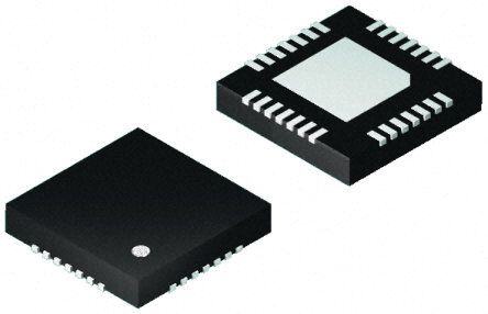
| 供应商器件封装 | 28-VQFN (5x5) |
| 共模抑制比—最小值 | 54 dB |
| 其它名称 | 296-25578-6 |
| 制造商产品页 | http://www.ti.com/general/docs/suppproductinfo.tsp?distId=10&orderablePartNumber=PGA870IRHDT |
| 包装 | Digi-Reel® |
| 压摆率 | 2900 V/µs |
| 商标 | Texas Instruments |
| 增益带宽积 | - |
| 安装类型 | 表面贴装 |
| 安装风格 | SMD/SMT |
| 封装 | Reel |
| 封装/外壳 | 28-VFQFN 裸露焊盘 |
| 封装/箱体 | VQFN-28 |
| 工作温度 | -40°C ~ 85°C |
| 工作电源电压 | 5 V |
| 工厂包装数量 | 250 |
| 带宽 | 650 MHz |
| 放大器类型 | 可编程增益 |
| 最大功率耗散 | 2.9 W |
| 最大工作温度 | + 85 C |
| 最大输入电阻 | 173 Ohms |
| 最小工作温度 | - 40 C |
| 标准包装 | 1 |
| 电压-电源,单/双 (±) | 4.75 V ~ 5.25 V |
| 电压-输入失调 | - |
| 电流-电源 | 143mA |
| 电流-输入偏置 | - |
| 电流-输出/通道 | 50mA |
| 电源电流 | 143 mA |
| 电路数 | 1 |
| 稳定时间 | 3 ns |
| 系列 | PGA870 |
| 转换速度 | 2900 V/us |
| 输入补偿电压 | +/- 5 mV |
| 输出电流 | 50 mA |
| 输出类型 | - |


- 商务部:美国ITC正式对集成电路等产品启动337调查
- 曝三星4nm工艺存在良率问题 高通将骁龙8 Gen1或转产台积电
- 太阳诱电将投资9.5亿元在常州建新厂生产MLCC 预计2023年完工
- 英特尔发布欧洲新工厂建设计划 深化IDM 2.0 战略
- 台积电先进制程称霸业界 有大客户加持明年业绩稳了
- 达到5530亿美元!SIA预计今年全球半导体销售额将创下新高
- 英特尔拟将自动驾驶子公司Mobileye上市 估值或超500亿美元
- 三星加码芯片和SET,合并消费电子和移动部门,撤换高东真等 CEO
- 三星电子宣布重大人事变动 还合并消费电子和移动部门
- 海关总署:前11个月进口集成电路产品价值2.52万亿元 增长14.8%


PDF Datasheet 数据手册内容提取
PGA870 PGA870 www.ti.com SBOS436A–DECEMBER2009–REVISEDFEBRUARY2011 High-Speed, Fully Differential, Programmable-Gain Amplifier CheckforSamples:PGA870 FEATURES DESCRIPTION 1 • Wideband+5-VOperation:650-MHzBandwidth The PGA870 is a wideband programmable-gain 23 • LowImpedance,VoltageModeOutput amplifier (PGA) for high-speed signal chain and data acquisition systems. The PGA870 has been • WideGainRange:–11.5dBto+20dB optimized to provide high bandwidth, low distortion, • Precise0.5-dBGainSteps and low noise, making it ideally suited as a 14-bit Step-to-StepGainError=±0.03dB analog-to-digital converter (ADC) driver for wireless • HD :–93dBcat100MHz base station signal chain applications. The wide gain 2 range of –11.5 dB to +20 dB can be adjusted in • HD :–88dBcat100MHz 3 0.5-dB gain steps through a 6-bit control word applied • IMD :–98dBcat100MHz,–95dBcat200MHz 3 to the parallel interface. The gain control interface • OIP3:+47dBmat100MHz; may be configured as a level-triggered latch or an Exceeds+45dBmforFrequenciesto300MHz edge-triggered latch, or it may be placed in an unlatched (transparent) mode. In addition to the 6-bit • FlexibleGainControlInterface: gain control, the PGA870 contains a power-down pin – Supportslatchedandunlatchedoptions (PD) that can be used to put the device into a – Gainmaybesetinpower-downstate low-current, power-down mode. In this mode, the quiescent current drops to 2 mA, but the gain control – Fastsetupandholdtimes:2.5ns circuitry remains active, allowing the gain of the • LowDisableCurrent:2mA PGA870 to be set before device power-up. The • Pb-Free(RoHS-Compliant)andGreenPackage PGA870 is offered in a QFN-28 PowerPAD™ package. APPLICATIONS RELATEDPRODUCTS • ProgrammableGainIFAmplifier: – Differentialsignalchains DEVICE DESCRIPTION – Single-endedtodifferentialconversion THS4509 Wideband,low-noise,low-distortion,fully differentialamplifier • FastGainControlLoopsfor: THS7700 High-speed,fullydifferential16-bitADCdriver – Test/measurement THS9000 50-MHzto400-MHzIF/RFAmplifier – Digitalradiosignalchains 14-Bit,250-MSPSADCwithDDR ADS6149 • ADCDriverforWirelessBaseStationSignal LVDS/CMOSOutputs Chains:GSM,WCDMA,MC-GSM ADS6145 14-Bit,125-MSPSADCwithDDR • Radar/RangingSystems LVDS/CMOSOutputs ADS58C48 QuadchannelIFreceiverwithSNRBoost3G 6b Gain Adjust Fast Gain Control Loop +5 V 6b Signal Source 6b FS= 250 MHz Programmable Attenuator BaFnidltpearss ADS6149 FPGA PGA870 Control Logic Latch Mode1 Powerdown 1 Gain Strobe 1 1 Pleasebeawarethatanimportantnoticeconcerningavailability,standardwarranty,anduseincriticalapplicationsofTexas Instrumentssemiconductorproductsanddisclaimerstheretoappearsattheendofthisdatasheet. PowerPADisatrademarkofTexasInstruments. 2 Allothertrademarksarethepropertyoftheirrespectiveowners. 3 PRODUCTIONDATAinformationiscurrentasofpublicationdate. ©2009–2011,TexasInstrumentsIncorporated Products conform to specifications per the terms of the Texas Instruments standard warranty. Production processing does not necessarilyincludetestingofallparameters.
PGA870 SBOS436A–DECEMBER2009–REVISEDFEBRUARY2011 www.ti.com This integrated circuit can be damaged by ESD. Texas Instruments recommends that all integrated circuits be handled with appropriateprecautions.Failuretoobserveproperhandlingandinstallationprocedurescancausedamage. ESDdamagecanrangefromsubtleperformancedegradationtocompletedevicefailure.Precisionintegratedcircuitsmaybemore susceptibletodamagebecauseverysmallparametricchangescouldcausethedevicenottomeetitspublishedspecifications. ORDERINGINFORMATION(1) SPECIFIED PACKAGE TEMPERATURE PACKAGE ORDERING TRANSPORTMEDIA, PRODUCT PACKAGE-LEAD DESIGNATOR RANGE MARKING NUMBER QUANTITY PGA870 PGA870IRHDT TapeandReel,250 PGA870 QFN-28 RHD –40°Cto+85°C PGA870 PGA870IRHDR TapeandReel,3000 (1) ForthemostcurrentpackageandorderinginformationseethePackageOptionAddendumattheendofthisdocument,orseetheTI websiteatwww.ti.com. ABSOLUTE MAXIMUM RATINGS(1) Overoperatingfree-airtemperaturerange,unlessotherwisenoted. PGA870 UNIT Powersupply 6 V Internalpowerdissipation SeeThermalCharacteristics Inputvoltagerange VS V Storagetemperaturerange –65to+150 °C Maximumjunctiontemperature(TJ) +150 °C Maximumjunctiontemperature(TJ),continuousoperation,long-termreliability +140 °C Humanbodymodel(HBM) 2000 V ESDrating Chargeddevicemodel(CDM) 1000 V Machinemodel(MM) 200 V (1) Stressesabovetheseratingsmaycausepermanentdamage.Exposuretoabsolutemaximumconditionsforextendedperiodsmay degradedevicereliability.Thesearestressratingsonly,andfunctionaloperationofthedeviceattheseoranyotherconditionsbeyond thosespecifiedisnotsupported. DISSIPATION RATINGS(1) POWERRATING(2) (T =+125°C) J PACKAGE θ (°C/W) θ (°C/W) T =+25°C T =+85°C JP JA A A QFN-28 4.1 35 2.9W 0.87W (1) ThesedataweretakenwiththeJEDECHigh-KtestPCB.FortheJEDEClow-KtestPCB,θ is350°C/W. JA (2) Powerratingisdeterminedwithajunctiontemperatureof+125°C.Thisisthepointwheredistortionstartstosubstantiallyincreaseand long-termreliabilitystartstobereduced.Thermalmanagementofthefinalprintedcircuitboardshouldstrivetokeepthejunction temperatureatorbelow+125°Cforbestperformanceandreliability. 2 ©2009–2011,TexasInstrumentsIncorporated ProductFolderLink(s):PGA870
PGA870 www.ti.com SBOS436A–DECEMBER2009–REVISEDFEBRUARY2011 ELECTRICAL CHARACTERISTICS: V = +5 V S+ Boldfacelimitsaretestedat+25°C. AtT =+25°C,V =+5V,differentialinputsignal,differentialV =2V ,R =200Ωdifferential,G=20dB,andinputand A S+ OUT PP L outputcommon-modeatinternalmidsupplyreference,unlessotherwisenoted. PGA870IRHD TEST PARAMETER CONDITIONS MIN TYP MAX UNITS LEVEL(1) ACPERFORMANCE Small-signalbandwidth G=20dB,VO=100mVPP 650 MHz C Large-signalbandwidth G=20dB,VO=2VPP 650 MHz C Bandwidthfor0.1-dBflatness 100 MHz C Slewrate(differential) 2-Vstep 2900 V/µs C Risetime 2-Vstep 0.55 ns C Falltime 2-Vstep 0.55 ns C Settlingtimeto1% 2-Vstep 3 ns C Settlingtimeto0.1% 2-Vstep 5 ns C Noisefigure 150-Ωsystem,Gain=+20dB,f=100MHz 13 dB C Gain=+20dB,f>1MHz 30 nV/√Hz C Output-referredvoltagenoise Gain=–11dB,f>1MHz 40 nV/√Hz C HARMONICDISTORTION Gain=+20dB,VO=2VPP,RL=200Ω f=50MHz –108 dBc C Second-orderharmonicdistortion f=100MHz –93 dBc C f=200MHz –71 dBc C f=50MHz –95 dBc C Third-orderharmonicdistortion f=100MHz –88 dBc C f=200MHz –75 dBc C f1(MHz) f2(MHz) C Second-orderintermodulation 2-MHztone 49 51 -87 dBc C distortion spacing 99 101 -90 dBc C 199 201 -89 dBc C 49 51 -103 dBc C 2-MHztone Third-orderintermodulationdistortion 99 101 –98 dBc C spacing 199 201 –95 dBc C 49 51 50 dBm C Outputthird-orderintercept VOUT=2VPP, 99 101 47 dBm C RL=200Ω 199 201 45 dBm C DC TA=+25°C –30 ±5 30 mV A Outputoffsetvoltage TA=–40°Cto+85°C –35 35 mV B Averageoffsetvoltagedrift TA=–40°Cto+85°C 20 μV/°C B INPUT Inputreturnloss ZSYS=150Ω,frequency<300MHz -40 dB B Differentialinputresistance 129 150 173 Ω B Differentialinputcapacitance 1.2 pF C Single-endedinputresistance 141 Ω B Common-moderejectionratio TA=+25°C,Gain=20dB 54 76 dB A (1) Testlevels:(A)100%testedat+25°C.Overtemperaturelimitssetbycharacterizationandsimulation.(B)Limitssetbycharacterization andsimulation.(C)Typicalvalue;onlyforinformation. ©2009–2011,TexasInstrumentsIncorporated 3 ProductFolderLink(s):PGA870
PGA870 SBOS436A–DECEMBER2009–REVISEDFEBRUARY2011 www.ti.com ELECTRICAL CHARACTERISTICS: V = +5 V (continued) S+ Boldfacelimitsaretestedat+25°C. AtT =+25°C,V =+5V,differentialinputsignal,differentialV =2V ,R =200Ωdifferential,G=20dB,andinputand A S+ OUT PP L outputcommon-modeatinternalmidsupplyreference,unlessotherwisenoted. PGA870IRHD TEST PARAMETER CONDITIONS MIN TYP MAX UNITS LEVEL(1) OUTPUT TA=+25°C 3.5 3.7 V A Maximumoutputvoltagehigh Eachoutputwith TA=–40°Cto+85°C 3.4 V B 100Ωto midsupply TA=+25°C 1.3 1.5 V A Minimumoutputvoltagelow TA=–40°Cto+85°C 1.6 V B TA=+25°C,RL=200Ω 4 4.8 VPP B Differentialoutputvoltageswing TA=–40°Cto+85°C 3.6 VPP B Differentialoutputcurrentdrive TA=+25°C,RL=20Ω 40 50 mAP A Outputcommon-modeoffsetfrom midsupply TA=+25°C,RL=20Ω –60 ±10 60 mV A Differentialoutputimpedance f=100MHz 3.5/87 Ω/° B Differentialoutputimpedancemodel SeriesROUT,EQ,LOUT,EQ 0.3/3.8 Ω/nH B POWERSUPPLY Specifiedoperatingvoltage 4.75 5 5.25 V C TA=+25°C 138 143 148 mA A Quiescentcurrent TA=–40°Cto+85°C 136 150 mA B Power-supplyrejectionratio(PSRR) TA=+25°C,Gain=20dB(2) 54 76 dB A POWERDOWN Devicepower-upvoltagethreshold Ensuredonabove2.1V 2.1 V A Devicepower-downvoltagethreshold Ensuredoffbelow0.9V 0.9 V A TA=+25°C 2 4 mA A Power-downquiescentcurrent TA=–40°Cto+85°C 4.8 mA B Forwardisolationinpower-downstate f=100MHz -110 dB C PDpininputbiascurrent PD=VS– 0.5 μA B PDpininputimpedance 20||0.5 kΩ||pF C Turn-ontimedelay Measuredtooutputon 16 ns C Turn-offtimedelay Measuredtooutputoff 60 ns C GAINSETTING Gainrange –11.5 +20 dB A Gaincontrol:G0toG5 6 Bits B Gainstepsize –11.5dB≤Gain≤+20dB 0.50 dB A Absolutegainerror –0.35 ±0.05 0.35 dB A Gainerroroverentiregainrange Steptostepgainerror –0.10 ±0.03 0.10 dB A Gaintempcoefficient 0.0018 0.0022 0.0026 dB/°C B Gainsettlingtime 5 ns B DIGITALINPUTS B0toB5andLatch Digitalthresholdlow 0.9 V A Digitalthresholdhigh 2.1 V A Currentinto/outofdigitalpins ±20 nA C DatasetuptimetoGAINSTROBElow 2.5 ns C DataholdtimeafterGAINSTROBE 0 ns C low Latencytime 6.4 ns C (2) PSRRisdefinedwithrespecttoadifferentialoutput. 4 ©2009–2011,TexasInstrumentsIncorporated ProductFolderLink(s):PGA870
PGA870 www.ti.com SBOS436A–DECEMBER2009–REVISEDFEBRUARY2011 PIN CONFIGURATION QFN-28 RHDPACKAGE (TOPVIEW) VMID1 PD GND VS+ GND GND GND 8 7 6 5 4 3 2 2 2 2 2 2 2 2 LATCH MODE 1 21 GND VS+ 2 20 VS+ IN+ 3 19 OUT+ VMID2 4 18 GND IN- 5 17 OUT- VS+ 6 PowerPADä 16 VS+ GAIN STROBE 7 15 GND 8 9 10 11 12 13 14 B5 B4 B3 S+ B2 B1 B0 B) V S M ( PINASSIGNMENTS PINNUMBER PINNAME DESCRIPTION Controlslatchedandunlatchedacquisitionofthegaincontrolword(B0toB5).SeetheapplicationsectionGain 1 LATCHMODE ControlModesforadetaileddescription. 2,6,11,16,20,25 VS+ +5Vpowersupply 3 IN+ Noninvertinginput Bufferoutputfortheinternalmidsupplyreference.Thispointistheoutputofanactivebufferwhichisnotintended 4 VMID2 todriveanexternalload.Itshouldbebypassedbya0.1-μFcapacitor. 5 IN– Invertinginput 7 GAINSTROBE Gainlatchclockpin 8 B5(MSB) GaincontrolMSB 9 B4 Gaincontrolbit4 10 B3 Gaincontrolbit3 12 B2 Gaincontrolbit2 13 B1 Gaincontrolbit1 14 B0(LSB) Gaincontrolbit0 17 OUT– Invertingoutput 15,18,21,22,23, GND Ground 24,26 19 OUT+ Noninvertingoutput 27 PD Activelowpower-downfordeviceanalogcircuitry.GaincontrolCMOScircuitryisstillactivewhenPDislow. Chipbypasspinforinternalmidsupplyreference.Thispointisthemidpointofaresistivevoltagedividerandisnot 28 VMID1 intendedtofunctionasaninput.Itshouldbebypassedwitha0.1-μFcapacitor. ThermalPad PowerPAD Thermalcontactforheatdissipation.Thethermalpadmustbeconnectedtoelectricalground. ©2009–2011,TexasInstrumentsIncorporated 5 ProductFolderLink(s):PGA870
PGA870 SBOS436A–DECEMBER2009–REVISEDFEBRUARY2011 www.ti.com TYPICAL CHARACTERISTICS AtT =+25°C,V =+5V,differentialinputsignal,differentialV =2V ,R =200Ωdifferential,G=+20dB,andinputand A S+ OUT PP L outputcommon-modeatinternalmidsupplyreference,unlessotherwisenoted. SMALL-SIGNALACRESPONSE SMALL-SIGNALACRESPONSE GainAdjustedfrom–11.5dBto+5dB GainAdjustedfrom+5.5dBto+20dB 10 25 Gain Adjusted in 0.5-dB Steps Gain = +5 dB Gain Adjusted in 0.5-dB Steps Gain = +20 dB V = 200 mV V = 200 mV OUT PP OUT PP 5 20 B) 0 B) 15 d d n ( n ( Gai -5 Gai 10 -10 5 Gain = +5.5 dB Gain =-11.5 dB -15 0 10 100 1000 10 100 1000 Frequency (MHz) Frequency (MHz) Figure1. Figure2. LARGE-SIGNALACRESPONSEATFOURGAINS LARGE-SIGNALACRESPONSEATFOURGAINS DIFFERENTIALINPUT SINGLE-ENDEDINPUT 30 30 25 25 Gain = 20 dB Gain = 20 dB 20 20 15 15 Gain = 10 dB Gain = 10 dB B) 10 B) 10 d d ain ( 5 Gain = 0 dB ain ( 5 Gain = 0 dB G 0 G 0 -5 Gain =-6 dB -5 Gain =-6 dB -10 -10 -15 Differential Input -15 Single-Ended Input V = 2 V V = 2 V -20 OUT PP -20 OUT PP 10 100 1000 10 100 1000 Frequency (MHz) Frequency (MHz) Figure3. Figure4. DIFFERENTIALFREQUENCYRESPONSEvsCAPACITIVE LOAD R vsCAPACITIVELOAD OS 25 100 C = 44 pF C = 94 pF L L C = L 20 10 pF C = 820 pF L dB) 15 C = 470 pF W) Gain ( 10 L CL= R(OS 10 ROS 16 pF ROS 5 PGA870 ROS CLVOUT C20L p=F PGA870 ROS CLVOUT CL CL 0 1 10 100 1000 1 10 100 1000 Frequency (MHz) Capacitive Load (pF) Figure5. Figure6. 6 ©2009–2011,TexasInstrumentsIncorporated ProductFolderLink(s):PGA870
PGA870 www.ti.com SBOS436A–DECEMBER2009–REVISEDFEBRUARY2011 TYPICAL CHARACTERISTICS (continued) AtT =+25°C,V =+5V,differentialinputsignal,differentialV =2V ,R =200Ωdifferential,G=+20dB,andinputand A S+ OUT PP L outputcommon-modeatinternalmidsupplyreference,unlessotherwisenoted. STEP-TO-STEPGAINERRORvsGAINSETTING LARGE-SIGNALGAINvsGAINSETTING OVERTEMPERATURE 25 0.15 -40°C 20 0.10 15 0.05 Gain (dB) 105 n Error (dB) -0.050 +25°C 0 ai G -5 -0.10 +85°C 50 MHz -10 100 MHz -0.15 200 MHz -15 -0.20 -12-10-8 -6 -4 -2 0 2 4 6 8 10 12 14 16 18 20 -12-10-8 -6 -4 -2 0 2 4 6 8 10 12 14 16 18 20 Gain Setting Gain Setting Figure7. Figure8. STEP-TO-STEPGAINERRORvsGAINSETTING OVERFREQUENCY GAINSTEPRESPONSE:NOLATCH 0.04 4.0 1.5 3.5 Gain Control Gain Code = 111111 0.02 1.0 3.0 Gain Error (dB) --00..00240 Gain Control (V) 22110.....50505 -000.5.5 Amplifier Output (V ) -0.06 50 MHz 0 -1.0 100 MHz -0.5 Amplifier Gain Code = 000000 200 MHz Output -0.08 -1.0 -1.5 -12-10-8 -6 -4 -2 0 2 4 6 8 10 12 14 16 18 20 0 100 200 300 400 500 Gain Setting Time (ns) Figure9. Figure10. GAINSTEPRESPONSE:LEVEL-TRIGGEREDGAINLATCH GAINSTEPRESPONSE:EDGE-TRIGGEREDLATCH V) V) Strobe ( 22..50 G11a1in1 1C1ode = Gain Strobe Strobe ( 22..50 Gain Code = 111111 SGtraoibne ain 1.5 ain 1.5 ol, G 1.0 ol, G 1.0 G00a0in0 0C0ode = ontr 0.5 ontr 0.5 C C ain 0 1.0 Am ain 0 1.0 Am G G00a0in0 0C0ode = 0.5 plifie G 0.5 plifie 0 r O 0 r O u u -0.5 tp -0.5 tp u u -1.0 t (V -1.0 t (V ) ) Time (50 ns/div) Time (50 ns/div) Figure11. Figure12. ©2009–2011,TexasInstrumentsIncorporated 7 ProductFolderLink(s):PGA870
PGA870 SBOS436A–DECEMBER2009–REVISEDFEBRUARY2011 www.ti.com TYPICAL CHARACTERISTICS (continued) AtT =+25°C,V =+5V,differentialinputsignal,differentialV =2V ,R =200Ωdifferential,G=+20dB,andinputand A S+ OUT PP L outputcommon-modeatinternalmidsupplyreference,unlessotherwisenoted. THIRD-ORDERINTERMODULATIONDISTORTION SECOND-ORDERINTERMODULATIONDISTORTION FORTWOGAINSANDFOUROUTPUTLOADS(V =2 OUT FORFOUROUTPUTLOADS(V =2V ) V ) OUT PP PP -70 -80 VOUT= 2 VPP -82 VOUT= 2 VPP -75 DF = 2 MHz --8846 DF = 2 MHz -88 -80 -90 c) c) -92 D(dB2 -85 D(dB3 --9946 M M -98 I --9905 RRRLLL=== 125000000WWW I ----111100000246 Dashed lines: Gain =-6 dB RRRLLL=== 125000000WWW Gain = +10 dB RL= 1 kW -108 Solid lines: Gain = +10 dB RL= 1 kW -100 -110 50 100 150 200 250 300 50 100 150 200 250 300 Frequency (MHz) Frequency (MHz) Figure13. Figure14. THIRD-ORDERINTERMODULATIONDISTORTION SECOND-ORDERINTERMODULATIONDISTORTION FORTWOGAINSANDFOUROUTPUTLOADS(V =2 OUT FORFOUROUTPUTLOADS(V =2V ) V ) OUT PP PP -70 -80 VOUT= 2 VPP RL= 100W -82 VOUT= 2 VPP -75 DF = 2 MHz RRL== 250000WW --8846 DF = 2 MHz RL= 1 kW -88 -80 L -90 c) c) -92 D(dB2 -85 D(dB3 --9946 M M -98 I -90 I -100 R = 100W -95 ---111000246 Dashed lines: Gain = 0 dB RRLLL== 250000WW Gain = +20 dB -108 Solid lines: Gain = +20 dB RL= 1 kW -100 -110 50 100 150 200 250 300 50 100 150 200 250 300 Frequency (MHz) Frequency (MHz) Figure15. Figure16. OUTPUTTHIRD-ORDERINTERCEPTvsFREQUENCY (V =2V ) OUT PP 50 V = 2 V OUT PP 48 RL= 200W 46 m) B 44 d ( P3 42 OI 40 Gain = +20 dB Gain = +10 dB 38 Gain = 0 dB Gain =-6dB 36 50 100 150 200 250 300 Frequency (MHz) Figure17. 8 ©2009–2011,TexasInstrumentsIncorporated ProductFolderLink(s):PGA870
PGA870 www.ti.com SBOS436A–DECEMBER2009–REVISEDFEBRUARY2011 TYPICAL CHARACTERISTICS (continued) AtT =+25°C,V =+5V,differentialinputsignal,differentialV =2V ,R =200Ωdifferential,G=+20dB,andinputand A S+ OUT PP L outputcommon-modeatinternalmidsupplyreference,unlessotherwisenoted. THIRD-ORDERINTERMODULATIONDISTORTION SECOND-ORDERINTERMODULATIONDISTORTION FORTWOGAINSANDFOUROUTPUTLOADS(V =3 OUT FORFOUROUTPUTLOADS(V =3V ) V ) OUT PP PP -70 -74 Gain = +10 dB -76 VOUT= 3 VPP -75 -78 DF = 2 MHz -80 -80 -82 c) c) -84 (dB -85 (dB -86 D2 D3 -88 M M -90 I -90 RL= 100W I -92 RL= 100W R = 200W -94 R = 200W L L -95 RRLL== 510 k0WW VDFOU =T 2= M3 HVzPP --9968 DSoalsidh elidn elisn:e Gs:a Gina =in + =10- 6d BdB RRLL== 510 k0WW -100 -100 50 100 150 200 250 300 50 100 150 200 250 300 Frequency (MHz) Frequency (MHz) Figure18. Figure19. THIRD-ORDERINTERMODULATIONDISTORTION SECOND-ORDERINTERMODULATIONDISTORTION FORTWOGAINSANDFOUROUTPUTLOADS(V =3 OUT FORFOUROUTPUTLOADS(V =3V ) V ) OUT PP PP -70 -74 VOUT= 3 VPP RL= 100W -76 RL= 100W VOUT= 3 VPP -75 DF = 2 MHz RL= 200W -78 RL= 200W DF = 2 MHz RL= 500W -80 RL= 500W -80 RL= 1 kW -82 RL= 1 kW c) c) -84 (dB -85 (dB -86 D2 D3 -88 M M -90 I -90 I -92 -94 -95 -96 Dashed lines: Gain = 0 dB Gain = +20 dB -98 Solid lines: Gain = +20 dB -100 -100 50 100 150 200 250 300 50 100 150 200 250 300 Frequency (MHz) Frequency (MHz) Figure20. Figure21. OUTPUTTHIRD-ORDERINTERCEPTvsFREQUENCY (V =3V ) OUT PP 52 V = 3 V OUT PP 50 RL= 200W 48 m) B 46 d ( P3 44 OI 42 40 Gain = +20 dB Gain = 0 dB Gain = +10 dB Gain =-6 dB 38 50 100 150 200 250 300 Frequency (MHz) Figure22. ©2009–2011,TexasInstrumentsIncorporated 9 ProductFolderLink(s):PGA870
PGA870 SBOS436A–DECEMBER2009–REVISEDFEBRUARY2011 www.ti.com TYPICAL CHARACTERISTICS (continued) AtT =+25°C,V =+5V,differentialinputsignal,differentialV =2V ,R =200Ωdifferential,G=+20dB,andinputand A S+ OUT PP L outputcommon-modeatinternalmidsupplyreference,unlessotherwisenoted. HARMONICDISTORTIONvsFREQUENCY HARMONICDISTORTIONvsFREQUENCY (V =2V ) (V =2V ) OUT PP OUT PP on (dBc) ---566505 VROLU=T 1=0 20 VWPP ---455505 Third-O on (dBc) ---566505 VROLU=T 2=0 20 VWPP ---455505 Third-O Distorti --7705 --6605 rder H Distorti --7705 --6605 rder H nic -80 -70 arm nic -80 -70 arm o o o o Second-Order Harm ---111---001899050505 GGaaiinn == D-0a6 ds SdBhoBeldid lilnineess:GG: 23aanriinndd ==HH aa++rr12mm00oo ddnnBBiicc ------7889915050500 nic Distortion (dBc) Second-Order Harm ---111---001899050505 GGaaiinn == D-0a6 ds SdBhoBeldid lilnineess:GG: 23aanriinndd ==HH aa++rr12mm00oo ddnnBBiicc ------7889915050500 nic Distortion (dBc) 0 50 100 150 200 250 300 0 50 100 150 200 250 300 Frequency (MHz) Frequency (MHz) Figure23. Figure24. HARMONICDISTORTIONvsFREQUENCY HARMONICDISTORTIONvsFREQUENCY (V =2V ) (V =2V ) OUT PP OUT PP on (dBc) ---566505 VROLU=T 5=0 20 VWPP ---455505 Third-O on (dBc) ---566505 VROLU=T 1= k2W VPP ---455505 Third-O Distorti --7705 --6605 rder H Distorti --7705 --6605 rder H nic -80 -70 arm nic -80 -70 arm o o o o Second-Order Harm ---111---001899050505 GGaaiinn D==a -0sS6 hdo edBldiBd lilnineess:: GG 23naarddiinn HH==aa ++rrmm1200oo nnddiiBBcc ------7889915050500 nic Distortion (dBc) Second-Order Harm ---111---001899050505 GGaaiinnD ==a s-0Sh6 ode ldBdidB lilnineess:: GG 23naarddiinn HH ==aa ++rrmm1200oo nnddiiBBcc ------7889915050500 nic Distortion (dBc) 0 50 100 150 200 250 300 0 50 100 150 200 250 300 Frequency (MHz) Frequency (MHz) Figure25. Figure26. 10 ©2009–2011,TexasInstrumentsIncorporated ProductFolderLink(s):PGA870
PGA870 www.ti.com SBOS436A–DECEMBER2009–REVISEDFEBRUARY2011 TYPICAL CHARACTERISTICS (continued) AtT =+25°C,V =+5V,differentialinputsignal,differentialV =2V ,R =200Ωdifferential,G=+20dB,andinputand A S+ OUT PP L outputcommon-modeatinternalmidsupplyreference,unlessotherwisenoted. HARMONICDISTORTIONvsFREQUENCY HARMONICDISTORTIONvsFREQUENCY (V =3V ) (V =3V ) OUT PP OUT PP on (dBc) ---566505 VROLU=T 1=0 30 VWPP ---445050 Third-O on (dBc) ---566505 VROLU=T 2=0 30 VWPP ---445050 Third-O Distorti --7705 --5650 rder H Distorti --7705 --5650 rder H nic -80 -65 arm nic -80 -65 arm o o o o Second-Order Harm ---111---001899050505 GGaaiinn == D-0a6 ds SdBhoBeldid lilnineess:GG: 23aanriinndd ==HH aa++rr12mm00oo ddnnBBiicc ------778899050505 nic Distortion (dBc) Second-Order Harm ---111---001899050505 GGaaiinn == D-0a6 ds SdBhoBeldid lilnineess:GG: 23aanriinndd ==HH aa++rr12mm00oo ddnnBBiicc ------778899050505 nic Distortion (dBc) 0 50 100 150 200 250 300 0 50 100 150 200 250 300 Frequency (MHz) Frequency (MHz) Figure27. Figure28. HARMONICDISTORTIONvsFREQUENCY HARMONICDISTORTIONvsFREQUENCY (V =3V ) (V =3V ) OUT PP OUT PP on (dBc) ---566505 VROLU=T 5=0 30 VWPP ---445050 Third-O on (dBc) ---566505 VROLU=T 1= k3W VPP ---445050 Third-O Distorti --7705 --5650 rder H Distorti --7705 --5650 rder H nic -80 -65 arm nic -80 -65 arm o o o o Second-Order Harm ---111---001899050505 GGaaiinn == D-0a6 ds SdBhoBeldid lilnineess:GG: 23aanriinndd ==HH aa++rr12mm00oo ddnnBBiicc ------778899050505 nic Distortion (dBc) Second-Order Harm ---111---001899050505 GGaaiinn == D-0a6 ds SdBhoBeldid lilnineess:GG: 23aanriinndd ==HH aa++rr12mm00oo ddnnBBiicc ------778899050505 nic Distortion (dBc) 0 50 100 150 200 250 300 0 50 100 150 200 250 300 Frequency (MHz) Frequency (MHz) Figure29. Figure30. ©2009–2011,TexasInstrumentsIncorporated 11 ProductFolderLink(s):PGA870
PGA870 SBOS436A–DECEMBER2009–REVISEDFEBRUARY2011 www.ti.com TYPICAL CHARACTERISTICS (continued) AtT =+25°C,V =+5V,differentialinputsignal,differentialV =2V ,R =200Ωdifferential,G=+20dB,andinputand A S+ OUT PP L outputcommon-modeatinternalmidsupplyreference,unlessotherwisenoted. OUTPUTVOLTAGENOISEvsFREQUENCY NOISEFIGUREvsGAIN 1000 45 f = 100 MHz )z 40 RSYS= 150W H ? age Noise (nV/ 100 e Figure (dB) 332505 ut Volt Nois 20 p ut O Gain = +20 dB 15 Gain =-11.5 dB 10 10 10 100 1 k 10 k 100 k 1 M 10 M 100 M -12-10-8 -6 -4 -2 0 2 4 6 8 10 12 14 16 18 20 22 Frequency (Hz) Gain (dB) Figure31. Figure32. LARGE-ANDSMALL-SIGNAL DISABLESTEPRESPONSE DIFFERENTIALPULSERESPONSE 2.25 1.5 1.5 0.15 2.00 Disable Signal 1.2 V) Gain = 20 dB, RL= 200W S Disable Signal Amplitude (V) 1111000.......752075250505050 Amplifier Output 0000----0001...963....3692 Amplifier Output (V) Large-Signal Differential Output ( --1001....05050 Left Scale Right Scale 000--00..10..010550 mall-Signal Differential Output (V) -0.25 -1.5 -1.5 -0.15 100 200 300 400 500 0 5 10 15 20 25 Time (ns) Time (2.5 ns/div) Figure33. Figure34. FORWARDISOLATIONvsFREQUENCY INDISABLEDMODE DIFFERENTIALINPUTIMPEDANCE -60 160 4 Magnitude W) 150 0 ation (dB) -80 Magnitude ( 140 Phase -4 Input Imped Forward Isol --110200 put Impedance 111321000 ---81126 ance Phase ()° n I -140 100 -20 0 100 200 300 400 500 100 k 1 M 10 M 100 M 1 G Frequency (MHz) Frequency (Hz) Figure35. Figure36. 12 ©2009–2011,TexasInstrumentsIncorporated ProductFolderLink(s):PGA870
PGA870 www.ti.com SBOS436A–DECEMBER2009–REVISEDFEBRUARY2011 TYPICAL CHARACTERISTICS (continued) AtT =+25°C,V =+5V,differentialinputsignal,differentialV =2V ,R =200Ωdifferential,G=+20dB,andinputand A S+ OUT PP L outputcommon-modeatinternalmidsupplyreference,unlessotherwisenoted. DIFFERENTIALINPUTRETURNLOSS SINGLE-ENDEDINPUTRETURNLOSS vsFREQUENCY vsFREQUENCY 0 0 ZSYS= 150W ZSYS= 150W -10 -5 Loss (dB) -20 Loss (dB) --1105 n -30 n etur etur -20 R R put -40 20 dB put -25 20 dB n n I 10 dB I 10 dB -50 0 dB -30 0 dB -6 dB -6 dB -60 -35 100 M 1 G 10 M 100 M 1 G Frequency (Hz) Frequency (Hz) Figure37. Figure38. DIFFERENTIALOUTPUTSWING DIFFERENTIALOUTPUTIMPEDANCE vsR LOAD 100 100 5.5 W) Phase 90 ude ( 80 Outp g (V) 5.0 utput Impedance Magnit 101 Magnitude 765432000000 ut Impedance Phase ()° Differential Output Swin 44..50 O 10 0.1 0 3.5 10 k 100 k 1 M 10 M 100 M 300 M 100 1 k 10 k Frequency (Hz) Differential Load Resistance, R (W) LOAD Figure39. Figure40. PSRRANDCMRR vsFREQUENCY 90 pply Rejection Ratio (dB)Mode Rejection Ratio (dB) 876543000000 CMRR PSRR Sun- er-mo 20 wm PoCo 10 0 1 k 10 k 100 k 1 M 10 M 100 M 1 G Frequency (Hz) Figure41. ©2009–2011,TexasInstrumentsIncorporated 13 ProductFolderLink(s):PGA870
PGA870 SBOS436A–DECEMBER2009–REVISEDFEBRUARY2011 www.ti.com APPLICATION INFORMATION Device Operation The PGA870 is a wideband, fully differential, programmable-gain amplifier. Looking at the block diagram in Figure42,thePGA870canbeseparatedintothefollowingfunctionalblocks: • InputAttenuator • BufferedMUX • OutputAmplifier • 8-bitdigitalinterface • Powerfunction Attenuator 1 IN- VS 2 Gain = +20 dB OUT- Buffered Output VMID2 MUX Amp OUT+ 7 IN+ 8 BIAS Gain Control Control PGA870 Gain Latch B0 B1 B2 B3 B4 B5 Disable Strobe Mode (LSB) (MSB) Figure42. PGA870BlockDiagram InputAttenuator The input stage of the PGA870 consists of a logarithmic R2R ladder and presents a 150-Ω load to the previous stage. To minimize input return loss and noise figure, it is recommended to provide a 150-Ω matching for that input.Thisinputcanbedriveneitherdifferentiallyorsingle-ended. This resistive input network is internally biased to midsupply by an internal buffer (V on pin 4). Proper MID2 bypassing is required on this node (0.1 μF). The buffer midsupply is generated by a passive resistor network (V on pin 28). A 0.1-μF capacitor is expected on V for adequate bypassing. Although V and V are MID1 MID1 MID1 MID2 externally accessible, neither of these pins is intended to be externally driven. Additionally, V is not intended MID2 todrivethemidsupplyreferencetoanotherchip,butcansourceapproximately200μAifrequired. During power-down operation, the input maintains its nominal differential resistance. However, V and V MD1 MID2 fall to 0 V. The input attenuator is controlled via the three most significant bits (MSBs) of the gain control. Refer toTable1forthestepsizeofeachofthesethreeMSBs. InputAmplifierandBufferedMUX Following the input attenuator is a programmable buffer stage; the gain of the programmable buffer is controlled by the three least significant bits (LSBs) of the gain-control word. Refer to Table 1 for the step size of each of thesethreeLSBs. Table1.GainBitsandCorrespondingGainStepSizes(indB) (MSB) (LSB) B5 B4 B3 B2 B1 B0 16 8 4 2 1 0.5 14 ©2009–2011,TexasInstrumentsIncorporated ProductFolderLink(s):PGA870
PGA870 www.ti.com SBOS436A–DECEMBER2009–REVISEDFEBRUARY2011 OutputAmplifier The PGA870 has a differential, voltage-mode output stage with a differential output resistance of approximately 0.3Ωandaninductivereactanceequivalentto3.8nH.Thecommon-modeoutputvoltagehasanominalvalueof V .Thisoutputamplifierhasanominalgainof+20dB. MID2 The nominal load is 200 Ω, but the PGA870 can drive loads as low as 100 Ω with only minor changes to the devicedistortion. Theoutputpinsgotoahigh-impedancestatewhenthedeviceisthepower-downstate(thatis,whenPDislow). 8-bitDigitalInterface The 8-bit digital interface is composed of six bits: three MSBs that control the input attenuation and three LSBs thatcontroltheinputamplifierandbufferedMUX.Formoreinformationonthisparallelinterface,refertotheGain ControlandLatchModessection. PowerFunction The PGA870 features a low-power disabled state for the analog circuitry when the power-down (PD) pin is low. In the disabled state, the digital circuitry remains active, which allows the gain to be set before device power-up. There is no internal circuitry to provide a nominal bias to this pin. If this pin is to be left open, it must be biased withanexternalpull-upresistor. Note that when the PGA870 is in this low-power mode, the gain can be programmed using the 8-bit digital interface, the output pins go to a high-impedance state, and the voltage on the midsupply pins biasing the attenuator(pin4andpin28)goesto0V. Gain Control and Latch Modes The PGA870 has six bits of gain control (B5 to B0) that give an extended gain range from a maximum gain of 20 dB to a minimum gain of –11.5 dB. The LSB (B0) represents a minimum gain change (step size) of 0.5 dB, and the LSB (B5) represents a gain change of 16 dB. The equivalent gain step size of each gain control bit is shown inTable1.ThedevicevoltagegaincanbeexpressedbyEquation1: Gain =20dB− 0.5dB× (N −63) (1) dB G N is the equivalent base-10 integer number that corresponds to the binary gain control word. A summary of the G 63possibledevicegainsversusNGandthevaluesofB0toB5areshowninTable2. The high and low voltage thresholds allow all of the gain control pins to be controlled by CMOS circuitry. There are no internal pull-up resistors on the gain-control pins. If the pins are to be left open, they must be biased with externalpull-upresistors. The PGA870 can be configured so the device gain is controlled by only the six gain bits (no latch) when the GAIN STROBE pin and the GAIN MODE pin are both held high. In this operating mode, the device voltage gain follows the signals on pins B0 to B5. Transients on the six gain bits can cause changes to the PGA870 gain while in this mode, as well. To combat this possibility, the PGA870 also supports two gain modes where the gain bitdataareacquiredandlatchedbysignalsontheGAINSTROBEpin. The device is configured for a level-triggered latch when the LATCH MODE pin is high; this configuration allows the six gain bits to be acquired and latched only on a high signal on the GAIN STROBE. When the GAIN STROBE signal goes low, the gain-control data are latched and the PGA870 gain is independent of the six gain bitsuntiltheGAINSTROBEgoeshighagain. If the PGA870 LATCH MODE pin is low, the device is configured for an edge-triggered latch that acquires and latchesthesixgain-controlbitsonlyonthefallingedgeoftheGAINSTROBEsignal. ©2009–2011,TexasInstrumentsIncorporated 15 ProductFolderLink(s):PGA870
PGA870 SBOS436A–DECEMBER2009–REVISEDFEBRUARY2011 www.ti.com Table2.PGA870GainandCorrespondingGainWordValues Gain Gain State Gain (MSB) (LSB) State Gain (MSB) (LSB) NG (dB) B5 B4 B3 B2 B1 B0 NG (dB) B5 B4 B3 B2 B1 B0 63 20 1 1 1 1 1 1 31 4 0 1 1 1 1 1 62 19.5 1 1 1 1 1 0 30 3.5 0 1 1 1 1 0 61 19 1 1 1 1 0 1 29 3 0 1 1 1 0 1 60 18.5 1 1 1 1 0 0 28 2.5 0 1 1 1 0 0 59 18 1 1 1 0 1 1 27 2 0 1 1 0 1 1 58 17.5 1 1 1 0 1 0 26 1.5 0 1 1 0 1 0 57 17 1 1 1 0 0 1 25 1 0 1 1 0 0 1 56 16.5 1 1 1 0 0 0 24 0.5 0 1 1 0 0 0 55 16 1 1 0 1 1 1 23 0 0 1 0 1 1 1 54 15.5 1 1 0 1 1 0 22 -0.5 0 1 0 1 1 0 53 15 1 1 0 1 0 1 21 -1 0 1 0 1 0 1 52 14.5 1 1 0 1 0 0 20 -1.5 0 1 0 1 0 0 51 14 1 1 0 0 1 1 19 -2 0 1 0 0 1 1 50 13.5 1 1 0 0 1 0 18 -2.5 0 1 0 0 1 0 49 13 1 1 0 0 0 1 17 -3 0 1 0 0 0 1 48 12.5 1 1 0 0 0 0 16 -3.5 0 1 0 0 0 0 47 12 1 0 1 1 1 1 15 -4 0 0 1 1 1 1 46 11.5 1 0 1 1 1 0 14 -4.5 0 0 1 1 1 0 45 11 1 0 1 1 0 1 13 -5 0 0 1 1 0 1 44 10.5 1 0 1 1 0 0 12 -5.5 0 0 1 1 0 0 43 10 1 0 1 0 1 1 11 -6 0 0 1 0 1 1 42 9.5 1 0 1 0 1 0 10 -6.5 0 0 1 0 1 0 41 9 1 0 1 0 0 1 9 -7 0 0 1 0 0 1 40 8.5 1 0 1 0 0 0 8 -7.5 0 0 1 0 0 0 39 8 1 0 0 1 1 1 7 -8 0 0 0 1 1 1 38 7.5 1 0 0 1 1 0 6 -8.5 0 0 0 1 1 0 37 7 1 0 0 1 0 1 5 -9 0 0 0 1 0 1 36 6.5 1 0 0 1 0 0 4 -9.5 0 0 0 1 0 0 35 6 1 0 0 0 1 1 3 -10 0 0 0 0 1 1 34 5.5 1 0 0 0 1 0 2 -10.5 0 0 0 0 1 0 33 5 1 0 0 0 0 1 1 -11 0 0 0 0 0 1 32 4.5 1 0 0 0 0 0 0 -11.5 0 0 0 0 0 0 Table3.GainControlSignalsandLatchModes LatchMode GAINSTROBE LATCHMODE CONDITION Devicegainfollowsandlatchesgaincontrolword(B0 Edge-triggeredlatch Fallingedge Low toB5)onlyonGAINSTROBEfallingedge. Devicegainfollowsgaincontrolword(B0toB5)when Level-triggeredlatch Low High GAINSTROBEandLATCHMODEarebothhigh. DevicegainlatcheswhenGAINSTROBEgoeslow. Devicegainislevel-triggeredonthegain-controlword Nolatch High High (B0toB5)whenLATCHMODEishighandGAIN STROBEremainshigh. 16 ©2009–2011,TexasInstrumentsIncorporated ProductFolderLink(s):PGA870
PGA870 www.ti.com SBOS436A–DECEMBER2009–REVISEDFEBRUARY2011 Table 3 and Figure 43 show a summary table and timing diagrams of the gain modes, respectively. Figure 44 illustrates a timing diagram that defines the transitions and timing of the set-up and hold times for both level-triggeredandedge-triggeredlatchmodes. Latched on Latched on No Latch Gain Strobe Gain Strobe Follows Falling Edge High Level Gain Control Word 1 Gain Strobe 0 1 Latch Mode 0 1 Gain Bits B5 to B0 (MSB to LSB) 0 1 Gain 0 Figure43. GainModeTiming 1 Gain Bits B5 to B0 (MSB to LSB) 0 t SU t HOLD 1 Gain Strobe 0 1 t LATENCY Gain 0 1 Latch Mode 0 Figure44. Set-UpandHoldTimes:Level-TriggeredandEdge-TriggeredLatchModes ©2009–2011,TexasInstrumentsIncorporated 17 ProductFolderLink(s):PGA870
PGA870 SBOS436A–DECEMBER2009–REVISEDFEBRUARY2011 www.ti.com Single-Ended to Differential Operation Figure 45 represents a single-ended to differential conversion test configuration with a 50-Ω source and a 200-Ω load. The midsupply pins V and V are properly bypassed; because this circuit is ac-coupled, these pins MID1 MID2 provide the biasing voltage required by the PGA870 input stage. The LATCH MODE, GAIN STROBE, and PD pins are connected to the supply voltage through a pull-up resistor. The PD pin set high powers up the PGA870, while setting the LATCH MODE and GAIN STROBE pins high bypasses the latch mode, allowing instantaneous gainchangesasB5toB0change.Onthenoninvertinginput,a75-Ω resistancewasaddedtoadaptthe150Ω to 50Ω andmatchthe50-Ω source. If a single-ended signal source is to be dc-coupled to the device, its voltage swing should be centered about the midsupply reference, V . If the input dc voltage is greater than 0.2 V from midsupply, then increased distortion MID1 and reduced performance can result. The non-driven input pin of the PGA870 should be ac-coupled to ground through a capacitor. In this configuration, the PGA870 amplifies the difference between the dc-coupled input signalandthemidsupplyreference. +5 V 1kW From 50-W Source 0.1mF IN+ (1) LM 75W (1) GS PD V MID2 OUT+ 0.1mF PGA870 200W V MID1 0.1mF OUT- B0 to B5 IN- 0.1mF B0 to B5 (1) LM=LATCHMODEpin(pin1),GS=GAINSTROBEpin(pin7). Figure45. BasicConnectionsforSingle-EndedtoDifferentialConversion 18 ©2009–2011,TexasInstrumentsIncorporated ProductFolderLink(s):PGA870
PGA870 www.ti.com SBOS436A–DECEMBER2009–REVISEDFEBRUARY2011 Differential-to-Differential Operation Differential operation of PGA870 is shown in Figure 46. In this example, both input pins are connected to a differential 150-Ω source. The PGA870 is driving a typical 200-Ω load. Both midsupply voltage pins V and MID1 V are bypassed with a 0.1-μF capacitor. The LATCH MODE, GAIN STROBE, and PD pins are connected to MID2 the power supply using a 1-kΩ pull-up resistor. The PD pin set high powers up the PGA870, while setting the Latch Mode and the Gain Strobe pins high bypasses the latch mode, allowing instantaneous gain changes as B5 toB0change. If a differential signal source is to be dc-coupled to the device, it should have a common-mode voltage that is within 0.2 V of the midsupply reference. If the input common-mode is greater than 0.2 V from midsupply, then increaseddistortionandreducedperformancecanresult. +5 V 1kW From 150-W Differential Source 0.1mF IN+ (1) LM (1) GS V PD 0.1mF MID2 OUT+ PGA870 200W V MID1 0.1mF OUT- B0 to B5 IN- 0.1mF B0 to B5 (1) LM=LATCHMODEpin(pin1),GS=GAINSTROBEpin(pin7). Figure46. BasicConnectionsforFullyDifferentialOperation Operation with Split Supply ±2.5 V The PGA870 can be operated using a split ±2.5-V supply. In this case, V is connected to +2.5 V, and GND S+ (and any other pin noted to be connected to GND) is connected to –2.5 V. As with any device, what the user decides to name the levels in the system is irrelevant to the PGA870. In essence, it is simply a level shift of the powerpinsandallvoltagelevelsby–2.5V.Witha±2.5-Vpowersupply,theoutputcommon-modevoltageis0V and input and output voltage ranges are symmetrical around 0 V. The power-down and gain control logic input thresholds all shift to relative to –2.5 V; that is, the logic low threshold of 0.9 V with a single 5-V supply shifts to 1.6 V with ±2.5-V supplies, and the logic high threshold of 2.1 V with a single 5-V supply shifts to –0.4 V with ±2.5-Vsupplies.Level-shiftingthelogicsignalsmayrequireacomparatorcircuitforeachlogicsignalline. ©2009–2011,TexasInstrumentsIncorporated 19 ProductFolderLink(s):PGA870
PGA870 SBOS436A–DECEMBER2009–REVISEDFEBRUARY2011 www.ti.com Figure 47 shows one possible circuit using one channel of the high-speed, 4.5-ns propagation delay TLV3502. Theswitchingspeedoftheoutputlogicsignalislimitedbythepropagationdelayofthecomparator.Usingslower comparators limits the digital logic speed and can thus limit the gain control speed in automatic gain control applications. +2.5 V 2.5-V Input Logic V = 2.1 V, V = 0.9 V OH OL +2.5 V 1/2 Logic to PGA870 Pin TLV3502 V = +2.5 V, V =-2.5 V R OH OL R -2.5 V Figure47. ComparatorCircuittoShiftLogicSignalstoPGA870OperatedonSplit±2.5-VSupplies Using the PGA870 with split ±2.5-V supplies allows for an input signal centered around ground and sets the output common mode of the PGA870 to ground. The ADC Input Common-Mode Voltage Considerations: DC-Coupled Input section discusses how an output common-mode voltage of 0 V provides less signal attenuation when using a level-translating resistor network to drive an ADC with a low input common-mode voltageindc-coupledapplications. Driving ADCs The PGA870 is designed and optimized to drive differential input ADCs for the lowest distortion performance. Figure 48 shows a generic block diagram of the PGA870 driving an ADC. The primary interface circuit between the amplifier and the ADC is a noise-limiting and anti-aliasing filter that may also provide a means to bias the signal to the input common-mode voltage required by the ADC. Filters range from single-order real RC poles to higher-order LC filters, depending on the application requirements. Output resistors (R ) are shown on the O amplifier outputs to isolate the amplifier from any capacitive loading presented by the filter as the PGA870 presentsalowimpedanceonitsoutputs. R O Bandpass A IN+ PGA870 Filter ADC and R Bias AIN- CM O Figure48. GenericADCDriverBlockDiagram KeypointstoconsiderforsuccessfullyimplementingthePGA870aredescribedinthefollowingsubsections. SNRConsiderations Depending on the amplitude of the signal and the bandwidth of the filter, the SNR of the amplifier and filter together can be calculated. Note that the noise from the amplifier is band-limited by the filter with the equivalent brick-wallfilterbandwidth.TheamplifierandfilternoisecanbecalculatedusingEquation2. ( V 2 ( ( V ( SNR = 10log O = 20log O Amp+Filter e2 e Filterout Filterout with: e = e ENB Filterout NAmpout (2) 20 ©2009–2011,TexasInstrumentsIncorporated ProductFolderLink(s):PGA870
PGA870 www.ti.com SBOS436A–DECEMBER2009–REVISEDFEBRUARY2011 e is the output noise density of the PGA870 (30 nV/√Hz), ENB is the brick-wall equivalent noise bandwidth NAmpout of the filter, and V is the amplifier output signal. For example, with a first-order (N = 1) bandpass or low-pass O filterwith30-MHzcutoff,theENBis1.57•f =1.57•30MHz=47.1MHz.Forsecond-order(N=2)filters,the –3dB ENBis1.22•f . –3dB Asthefilterorderincreases,theENBapproachesf (forN=3,ENB=1.15 •f ,andforN=4,ENB=1.13• –3dB –3dB f ). Both V and e are in RMS voltages. For example, with a 2-V (0.707-V ) output signal and –3dB O Filterout PP RMS 30-MHz first-order filter, the SNR of the amplifier and filter is 70.7 dB with e = 30 nV/√Hz • √47.1 MHz= 206 Filterout μV . RMS The signal-to-noise ratio (SNR) of the amplifier, filter, and ADC add in RMS fashion as shown in Equation 3 (SNRvaluesindB): SNRSystem=-20log 10-SNR1Am0p+Filter +10-SN1R0ADC (3) Using this equation, one can see that if the SNR of the amplifier + filter equals the SNR of the ADC, the combined SNR is 3 dB lower (that is, worse). For minimal impact (less than 1 dB) on the ADC SNR, the SNR of the amplifier and filter together should be ≥ 10 dB better than the ADC SNR. The combined SNR calculated in thismannerisaccuratetowithin±1dBofactualimplementation. SFDRConsiderations The SFDR of the amplifier is usually set by second-order or third-order harmonic distortion for single-tone inputs, and by second-order or third-order intermodulation distortion for two-tone inputs. Harmonics and second-order intermodulation distortion can be filtered to some degree by the filter, but third-order intermodulation spurious cannot be filtered. The ADC generates the same distortion products as the amplifier; however, as a result of the samplingandclockfeedthrough,additionalspurs(notlinearlyrelatedtotheinputsignal)arealsoadded. Whenthespursfromtheamplifierandfiltertogetherareknown,eachindividualspurcanbedirectlyaddedtothe samespurfromtheADCasshowninEquation4toestimatethecombinedspur(spuramplitudesindBc): HDxSystem=-20log 1-0HDxAm2p+0Filter +10-HD2x0ADC (4) Note that Equation 4 assumes the spurs are in phase, but generally provides a good estimate of the final combineddistortion. For example, if the spur of the amplifier + filter equals the spur of the ADC, the combined spur is 6 dB higher. To minimize the amplifier contribution (less than 1 dB) to the overall system distortion, it is important that the spur from the amplifier + filter be ~15 dB better than the converter. The combined spur calculated in this manner is usually accurate to within ±6 dB of actual implementation, but higher variations have been observed, especially insecond-orderharmonicperformanceasaresultofphaseshiftinthefilter. The worst-case spur calculation above assumes that the amplifier/filter spur of interest is in phase with the corresponding spur in the ADC, such that the two spur amplitudes can be added linearly. There are two phase shift mechanisms that cause the measured distortion performance of the amplifier-ADC chain to deviate from the expectedperformancecalculatedusingEquation4:common-modephaseshiftanddifferentialphaseshift. Common-mode phase shift is the phase shift seen equally in both branches of the differential signal path, including the filter. This common-mode phase shift nullifies the basic assumption that the amplifier/filter and ADC spur sources are in phase. This phase shift can lead to better performance than predicted as the spurs are phase shifted, and there is the potential for cancellation as the phase shift reaches 180°. However, there is a significant challenge when designing an amplifier-ADC interface circuit to take advantage of common-mode phase shift for cancellation: the phase characteristic of the ADC spur sources are unknown, and therefore the necessaryphaseshiftinthefilterandsignalpathforcancellationisunknown. ©2009–2011,TexasInstrumentsIncorporated 21 ProductFolderLink(s):PGA870
PGA870 SBOS436A–DECEMBER2009–REVISEDFEBRUARY2011 www.ti.com Differential phase shift is the difference in the phase response between the two branches of the differential filter signal path. Differential phase shift in the filter as a result of mismatched components caused by nominal tolerancecanseverelydegradetheeven-orderdistortionoftheamplifier-ADCchain.Thisconditionhasthesame effect as mismatched path lengths for the two differential traces, and causes more phase shift in one path than the other. Ideally, the phase response over frequency through the two sides of a differential signal path are identical, such that even-order harmonics remain optimally out of phase and cancel when the signal is taken differentially. However, if one side has more phase shift than the other, then the even-order harmonic cancellationisnotaseffective. Single-order RC filters cause very little differential phase shift with nominal tolerances of 5% or less, but higher-order LC filters are very sensitive to component mismatch. For instance, a third-order Butterworth bandpass filter with 100-MHz center frequency and 20-MHz bandwidth shows up to 20° differential phase imbalance in a Spice Monte Carlo analysis with 2% component tolerances. Therefore, while a prototype may work, production variance is unacceptable. In ac-coupled applications that require second- and higher-order filters between the PGA870 and ADC, a transformer or balun is recommended at the ADC input to restore the phase balance. For dc-coupled applications where a transformer or balun at the ADC input cannot be used, it is recommended to use first- or second-order filters to minimize the effects of differential phase shift as a result of componenttolerance. ADCInputCommon-ModeVoltageConsiderations:AC-CoupledInput The input common-mode voltage range of the ADC must be respected for proper operation. In an ac-coupled application between the amplifier and the ADC, the input common-mode voltage bias of the ADC is accomplished in different ways depending on the specific ADC. Some ADCs use internal bias networks, and the analog inputs are automatically biased to the required input common-mode voltage if the inputs are ac-coupled with capacitors (or if the filter between the amplifier and ADC is a bandpass filter). Other ADCs supply the required input common-mode voltage as a reference voltage output at a CM pin. With these types of ADCs, the ac-coupled input signal can be re-biased to the input common-mode voltage by connecting resistors from each input to the CM output of the ADC, as shown in Figure 49. However, the signal is attenuated because of the voltagedividercreatedbyR andR . CM O R O R CM A IN+ PGA870 ADC RCM AIN- CM R O Figure49. BiasingAC-CoupledADCInputswiththeADCCMOutput Thesignalcanbere-biasedwhenaccoupling,andthereforethe output common-mode voltage of the amplifier is adon’tcarefortheADC. 22 ©2009–2011,TexasInstrumentsIncorporated ProductFolderLink(s):PGA870
PGA870 www.ti.com SBOS436A–DECEMBER2009–REVISEDFEBRUARY2011 ADCInputCommon-ModeVoltageConsiderations:DC-CoupledInput DC-coupled applications vary in complexity and requirements depending on the ADC; one requirement is the need to resolve the mismatch between the common-mode voltage of the driving amplifier and the ADC. For example, while the PGA870 has a fixed output common-mode of midsupply, or 2.5 V on a single 5-V supply, the ADS6149requiresanominal1.5-Vinputcommon-mode.TheADS58C48andADS4149,however,bothrequirea nominal 0.95-V input common-mode. As Figure 50 shows, a resistor network can be used to perform a common-mode level shift. This resistor network consists of the amplifier series output resistors and pull-up or pull-down resistors to a reference voltage. This resistor network introduces signal attenuation that may prevent the use of the full-scale input range of the ADC. ADCs with an input common-mode closer to the PGA870 output common-modeof2.5Vareeasiertouseinadc-coupledconfiguration,andrequirelittleornolevelshifting. V REF R VAMP+ RO P VADC+ ADC Amp R C IN IN VAMP- RO R VADC- P V REF Figure50. ResistorNetworktoDCLevel-ShiftCommon-ModeVoltage For common-mode analysis of the circuit in Figure 48, assume that V = V (for the PGA870, 2.5 V on a AMP± OCM single 5-V supply) and V = V (the specification for the ADC input common-mode voltage). V is chosen ADC± CM REF to be a voltage within the system greater than V (such as the ADC or amplifier analog supply) or ground, CM depending on whether the voltage must be pulled up or down, respectively, and R is chosen to be a reasonable O value,suchas24.9Ω.Withtheseknownvalues,R canbefoundbyusingEquation5. P V -V R = R ADC REF P O V -V AMP CM (5) Shifting the common-mode with the resistor network comes at the expense of signal attenuation. Modeling the ADC input as the parallel combination of a resistance R and capacitance C using values taken from the IN IN respective ADC data sheet, the approximate differential input impedance, Z , for the ADC can be calculated at IN thesignalfrequency.Thisimpedancecreatesadividerwiththeresistornetwork,whosegain(attenuation)canbe calculatedbyEquation6: 2R || Z GAIN = P IN 2R + 2R || Z O P IN (6) The introduction of the R resistors also modifies the effective load seen by the amplifier. The effective load seen P bytheamplifieristhencalculatedbyEquation7. R = 2R + 2R || Z L O P IN (7) The R resistors act in parallel to the ADC input such that the effective load (that is, the output current) seen by P the amplifier is increased. Higher current loads limit the PGA870 differential output swing and the typical distortionperformanceisonlyspecifiedforloadimpedancesof100-Ω differentialandgreater. Usingthegainandknowingthefull-scaleinputoftheADC,V ,therequiredamplitudetodrivetheADCwith ADC_FS thenetworkcanbecalculatedwithEquation8. V V = ADC_FS AMP_PP GAIN (8) ©2009–2011,TexasInstrumentsIncorporated 23 ProductFolderLink(s):PGA870
PGA870 SBOS436A–DECEMBER2009–REVISEDFEBRUARY2011 www.ti.com Using the ADC examples given previously, Table 4shows sample calculations of the value of R and V for P AMP_FS full-scaledrive,andthenfor–1dBFS. Table4.ExampleR forVariousADCs P ADC RIN||CIN VAMP_PP at for0 VAMP_PP VAMP VCM VREF 170MHz RO RP GAIN GAIN VADC_FS dBFS –1dBFS ADC (VDC) (VDC) (VDC) (Ω) (Ω) (Ω) (V/V) (dB) (VPP) (VPP) (VPP) ADS6149 2.5 1.5 0 216 25 37.5 0.53 –5.57 2 3.80 3.38 ADS58C48/ 2.5 0.95 0 195 25 15.3 0.35 –9.21 2 5.78 5.15 ADS4149 ADS58C48/ ADS4149(1) 0 0.95 2.5 195 25 40.8 0.53 –5.43 2 3.74 3.33 (1) PGA870operatedwith±2.5-Vsupply. As Table 4 shows, the signal attenuation as a result of the added resistor network increases as the required common-mode shift increases. For the ADS6149, the required common-mode level shift is –1 V, from 2.5 V to 1.5 V, and the signal attenuates by 5.57 dB. This difference is a significant signal loss, and the amplifier output must be increased (either by increasing the PGA870 input or the PGA870 gain) to make up for the loss in order to drive the full-scale input of the ADC for the highest SNR. At the same time, increasing the amplifier output swingresultsindegradeddistortionperformanceastheamplifieroutputapproachesitsoutputrangelimits. For the ADS58C48/ADS4149 case with the PGA870 operated with a single 5-V supply, the required level shift is –1.55 V and the signal attenuates by 9.21 dB. This signal loss cannot be fully recovered by increasing the PGA870 output: the differential output swing required at the PGA870 output to drive the full-scale range of the ADS58C48/ADS4149 exceeds the PGA870 output swing capability. Additionally, the distortion performance of the amplifier is degraded as the output swing increases. In these configurations, the maximum recommended ADC input is –6 dBFS in order to limit the impact of the additional loading. Another option is to operate the PGA870 with a split ±2.5-V supply, with the resulting calculations shown in the last row of Table 4. For this situation, if +2.5 V is used as the V pull-up voltage, the PGA870 only needs to drive 3.33 V at its output to REF PP drive the ADS58C48/ADS4149 input to –1 dBFS. See the Operation with Split Supply ±2.5V section for more detailsonusingthePGA870withsplitsupplies. Aswithanydesign,testingisrecommendedtovalidatewhethertheresultmeetsthespecificdesigngoals. PGA870 Driving ADS58C48 To illustrate the performance of the PGA870 as an ADC driver, the PGA870 is tested with the ADS58C48 and bandpass filter designs centered at an operating frequency of 170 MHz. The ADS58C48 is a quad-channel, 11-bit, 200-MSPS ADC with LVDS-compatible digital outputs on six data pairs per channel. The device has unbufferedanaloginputs.ThereareseveralkeyinformationpointstoconsiderwheninterfacingtothePGA870: • Unbufferedanaloginputswithafrequency-dependentinputimpedanceofZ =R ||C IN IN IN • 0.95-Vanaloginputcommon-modevoltage • SNR=66.1dBFS(typ)atf =170MHz IN • SFDR=80dBc(typ)atf =170MHz IN • HD =82dBc(typ)atf =170MHz 2 IN • HD =80dBc(typ)atf =170MHz 3 IN • IMD=83dBFS(typ)withtwo-toneinputf =185MHz,f =190MHz IN1 IN2 The ADS58C48EVM is designed for flexible options to ease design work. Used in conjunction with the TSW1200EVM High-Speed ADC LVDS Evaluation System, it reduces evaluation time to help the designer move fromprototypetoproductionmorequickly. The ADS58C48EVM provides back-to-back input transformers for each of the four analog input channels in order to convert single-ended test signals to differential when driving the ADCs directly. The Channel D path on the EVM, however, provides an alternate path (selectable via jumper resistors) for driving the channel with an onboard PGA870. In this path, a single-ended input test signal can be converted to differential with a single transformer to drive the PGA870 input. The EVM provides various component pads between the PGA870 and ADS58C48 input for implementing various filter types. For the latest schematic of the EVM, refer to the ADS58C48EVMDesignPackageavailablethroughtheADS58C48EVMproductpageontheTIwebsite. 24 ©2009–2011,TexasInstrumentsIncorporated ProductFolderLink(s):PGA870
PGA870 www.ti.com SBOS436A–DECEMBER2009–REVISEDFEBRUARY2011 Testing the PGA870 with a First-Order Bandpass Filter Differential phase shift in a differential filter because of component mismatches can lead to severely degraded even-order distortion performance. In applications where good SFDR performance at the expense of slight degradation in SNR is acceptable, a first-order filter can prove to be less sensitive and provide more repeatable resultscomparedtohigher-orderfilters. Figure 51 shows a simplified schematic of the PGA870 driving Channel D of the ADS58C48 on an ADS58C48EVM with a first-order bandpass filter designed for 50-MHz bandwidth at a center frequency of 170 MHz. As a result of board parasitics, the measured –3-dB bandwidth of the filter is 70 MHz. The measured –1-dB bandwidth of the filter is 40 MHz. At 20 dB of gain, the output voltage noise specification of the PGA870 is 30 nV/√Hz. With 2-V differential output swing and 70-MHz bandwidth, the expected SNR from the PP combined amplifier and filter is 68.7 dB. Added in combination with the ADS58C48 SNR, the expected SNR of theamplifier,filter,andADCchainis64dBFS. R2 C2 R10 25W 100 nF 15W ADC+ C18 R11 68 pF 100W L13 ADC V 8.2 nH CM C17 100 nF R1 100W R3 C3 R9 25W 100 nF 15W ADC- Figure51. First-OrderBandpassFilterSchematic Figure 52 shows the resulting FFT plot captured using the TSW1200 software with the PGA870 and first-order filterdrivingtheADSto–1dBFS,withasingle-toneinput170-MHzsinewavesampledat200MSPS.Theresults show 81.7-dBc SFDR and 63.7-dBFS SNR; analysis of the plot is provided in Table 5. The PGA870 is set to a maximum gain of 20 dB. Figure 53 shows the FFT plot with the PGA870 set to a gain of –4 dB, with the input signalamplitudeincreasedaccordinglytoachieve–1dBFSattheADCinput.Theresultsshow5dBlowerSFDR at this gain setting, which is expected at lower gains (see the Harmonic Distortion vs Frequency graphs, Figure23throughFigure30);however,theSNRremainsthesameatapproximately63.8dBFS. ©2009–2011,TexasInstrumentsIncorporated 25 ProductFolderLink(s):PGA870
PGA870 SBOS436A–DECEMBER2009–REVISEDFEBRUARY2011 www.ti.com Figure52. FFTPlotofPGA870(G=20dB)+First-OrderBandpassFilterandADS58C48with Single-ToneInputat170MHz Figure53. FFTPlotofPGA870(G=–4dB)+First-OrderBandpassFilterandADS58C48with Single-ToneInputat170MHz Table5.AnalysisofFFTforPGA870(G=20dB)+First-OrderBandpassFilter andADS58C48at170MHzvsTypicalADCSpecifications CONFIGURATION ADCINPUT SNR HD HD 2 3 PGA870+ First-order –1dBFS 63.7dBFS –83.8dBc –81.7dBc BandpassFilter andADS58C48 ADS58C48Only –1dBFS 66.1dBFS –82dBc –80dBc (typ) 26 ©2009–2011,TexasInstrumentsIncorporated ProductFolderLink(s):PGA870
PGA870 www.ti.com SBOS436A–DECEMBER2009–REVISEDFEBRUARY2011 Figure 54 and Figure 55 each show the FFT plots for the same first-order bandpass filter circuit with two-tone inputs, with each tone at –7 dBFS and the PGA870 set to a gain of 20 dB. Figure 54 shows the FFT for two-tone inputs at 160 MHz and 170 MHz. The third-order intermodulation distortion products at 150 MHz and 180 MHz are less than –86 dBc. Figure 55 shows the FFT for two-tone inputs at 168 MHz and 170 MHz. The highest spur isthethird-orderintermodulationproductat172MHzat–85dBFS. Figure54. FFTPlotofPGA870(G=20dB)+First-OrderBandpassFilterandADS58C48withTwo-Tone Inputsat160MHzand170MHz Figure55. FFTPlotofPGA870(G=20dB)+First-OrderBandpassFilterandADS58C48withTwo-Tone Inputsat168MHzand170MHz ©2009–2011,TexasInstrumentsIncorporated 27 ProductFolderLink(s):PGA870
PGA870 SBOS436A–DECEMBER2009–REVISEDFEBRUARY2011 www.ti.com Testing the PGA870 with a Second-Order Bandpass Filter For better combined SNR performance, narrower bandwidth and/or higher-order filters are required between the PGA870 and ADC. However, narrow filter bandwidth and highe-order filters cause the signal chain performance todependmorestronglyoncomponenttoleranceandmismatch.Componentvaluesthatare5%offfromnominal can detune a narrowband filter to the point that the desired signals do not fall within the useful passband and become attenuated. Mismatch between corresponding series components on the positive and negative sides of the differential filter can result in a differential phase shift that degrades even-order distortion performance. As mentioned in the SFDR Considerations section, a transformer or balun is recommended at the ADC input in these applications to restore the phase balance in the input signal to the ADC. The results shown in this discussion interface the PGA870 and filter directly to the ADS58C48 input, and other builds of the same filter on thesameEVMshowedover10dBofvariationindistortionperformance. Figure 56 shows a simplified schematic of the PGA870 driving Channel D of the ADS58C48 on an ADS58C48EVM with a second-order bandpass filter designed for 50-MHz bandwidth at a center frequency of 170 MHz. The measured –3-dB bandwidth of the filter is 57 MHz. The measured –1-dB bandwidth of the filter is 34 MHz. At a gain of 20 dB, the output voltage noise specification of the PGA870 is 30 nV/√Hz. With 2-V PP differential output swing and 57-MHz bandwidth, the expected SNR from the combined amplifier and filter is 70dB.AddedincombinationwiththetypicalADS58C48SNR,theexpectedSNRoftheamplifier,filter,andADC chainis64.5dBFS. R2 C21 L16 R10 25W 15 nF 56 nH 15W ADC+ R13 C10203 pF R10101W 49.9W L15 C20 ADC V 8.2 nH C17 CM 3.3 pF 100 nF R1 R12 100W 49.9W R3 C22 L17 R9 25W 15 nF 56 nH 15W ADC- Figure56. Second-OrderBandpassFilterSchematic Figure 57 shows the resulting FFT plot captured using the TSW1200 software with the PGA870 and a second-order filter driving the ADS to –1 dBFS, with a single-tone input 170-MHz sine wave sampled at 200 MSPS. The results show 87.76-dBc SFDR and 65-dBFS SNR; analysis of the plot is shown in Table 6. The PGA870issettoamaximumgainof20dB.Figure58showstheFFTplotwiththePGA870setinsteadtoagain of –4 dB, with the input signal amplitude increased accordingly to obtain –1 dBFS at the ADC input. The results showabout1dBlowerSFDRatthisgainsettingandnochangeintheSNR. 28 ©2009–2011,TexasInstrumentsIncorporated ProductFolderLink(s):PGA870
PGA870 www.ti.com SBOS436A–DECEMBER2009–REVISEDFEBRUARY2011 Figure57. FFTPlotofPGA870(G=20dB)+Second-OrderBandpassFilterandADS58C48with Single-ToneInputat170MHz Figure58. FFTPlotofPGA870(G=–4dB)+Second-OrderBandpassFilterandADS58C48with Single-ToneInputat170MHz Table6.AnalysisofFFTforPGA870(G=20dB)+Second-OrderBandpass FilterandADS58C48at170MHzvsTypicalADCSpecifications CONFIGURATION ADCINPUT SNR HD HD 2 3 PGA870+ Second-order –1dBFS 65dBFS –89.7dBc –90.8dBc BandpassFilter andADS58C48 ADS58C48Only –1dBFS 66.1dBFS –82dBc –80dBc (typ) ©2009–2011,TexasInstrumentsIncorporated 29 ProductFolderLink(s):PGA870
PGA870 SBOS436A–DECEMBER2009–REVISEDFEBRUARY2011 www.ti.com Figure 59 and Figure 60 show the FFT plots for the same second-order bandpass filter circuit with two-tone inputs, with each tone at –7 dBFS and the PGA870 set to a gain of 20 dB. Figure 59 shows the FFT for two-tone inputs at 160 MHz and 170 MHz. The third-order intermodulation distortion products at 150 MHz and 180 MHz are less than –90 dBc, though the second-order intermodulation distortion product at 10 MHz is at –82 dBc. Figure 60 shows the FFT for two-tone inputs at 168 MHz and 170 MHz. The near-in third-order intermodulation products at 166 MHz and 172 MHz are less than –88 dBFS, and the highest spur is the second-order intermodulationproductat2MHzat–81dBFS. Figure59. FFTPlotofPGA870(G=20dB)+Second-OrderBandpassFilterandADS58C48with Two-ToneInputsat160MHzand170MHz Figure60. FFTPlotofPGA870(G=20dB)+Second-OrderBandpassFilterandADS58C48with Two-ToneInputsat168MHzand170MHz 30 ©2009–2011,TexasInstrumentsIncorporated ProductFolderLink(s):PGA870
PGA870 www.ti.com SBOS436A–DECEMBER2009–REVISEDFEBRUARY2011 PCB Layout Recommendations Complete information about the PGA870EVM is found in the PGA870EVM User Guide, available for download through the PGA870 product folder on the TI web site. Printed circuit board (PCB) layout should follow these generalguidelines: 1. Signal routing should be direct and as short as possible into and out of the device input and output pins. Routingthesignalpathbetweenlayersusingviasshouldbeavoidedifpossible. 2. The device PowerPAD should be connected to a solid ground plane with multiple vias. The PowerPAD must beconnectedtoelectricalground.ConsultthePGA870EVMUserGuideforalayoutexample. 3. Groundorpowerplanesshouldberemovedfromdirectlyundertheamplifieroutputpins. 4. A0.1-μFcapacitorshouldbeplacedbetweentheV pinandgroundneartothepin. MID 5. Anoutputresistorisrecommendedineachoutputlead,placedasneartotheoutputpinsaspossible. 6. Two 0.1-μF power-supply decoupling capacitors should be placed as near to the power-supply pins as possible. 7. Two10-μFpower-supplydecouplingcapacitorsshouldbeplacedwithin1in(2,54cm)ofthedevice. 8. The digital control pins use CMOS logic levels for high and low signals, but can tolerate being pulled high to a+5-Vpowersupply.Thedigitalcontrolpinsdonothaveinternalpull-upresistors. ©2009–2011,TexasInstrumentsIncorporated 31 ProductFolderLink(s):PGA870
PGA870 SBOS436A–DECEMBER2009–REVISEDFEBRUARY2011 www.ti.com REVISION HISTORY NOTE:Pagenumbersforpreviousrevisionsmaydifferfrompagenumbersinthecurrentversion. ChangesfromOriginal(December,2009)toRevisionA Page • UpdatedRelatedProductstable ........................................................................................................................................... 1 • ChangedstoragetemperaturerangespecificationinAbsoluteMaximumRatingstable ..................................................... 2 • MovednoisefigureparametertoACPerformancesectionofElectricalCharacteristics(V =+5V)table ......................... 3 S • Addedoutput-referredvoltagenoiseparametertoElectricalCharacteristics(V =+5V)table .......................................... 3 S • AddedFigure31 ................................................................................................................................................................. 12 • RevisedsecondparagraphofSingle-EndedtoDifferentialOperationsection .................................................................. 18 • AddednewparagraphtoDifferential-to-DifferentialOperationsection .............................................................................. 19 • AddedOperationwithSplitSupply±2.5Vsection .............................................................................................................. 19 • AddedDrivingADCssection .............................................................................................................................................. 20 • AddedPGA870DrivingADS58C48section ....................................................................................................................... 24 • AddedTestingthePGA870withaFirst-OrderBandpassFiltersection ............................................................................ 25 • AddedTestingthePGA870withaSecond-OrderBandpassFiltersection ....................................................................... 28 32 ©2009–2011,TexasInstrumentsIncorporated ProductFolderLink(s):PGA870
PACKAGE OPTION ADDENDUM www.ti.com 6-Feb-2020 PACKAGING INFORMATION Orderable Device Status Package Type Package Pins Package Eco Plan Lead/Ball Finish MSL Peak Temp Op Temp (°C) Device Marking Samples (1) Drawing Qty (2) (6) (3) (4/5) PGA870IRHDR ACTIVE VQFN RHD 28 3000 Green (RoHS NIPDAU Level-2-260C-1 YEAR -40 to 85 PGA870 & no Sb/Br) IRHD PGA870IRHDT ACTIVE VQFN RHD 28 250 Green (RoHS NIPDAU Level-2-260C-1 YEAR -40 to 85 PGA870 & no Sb/Br) IRHD (1) The marketing status values are defined as follows: ACTIVE: Product device recommended for new designs. LIFEBUY: TI has announced that the device will be discontinued, and a lifetime-buy period is in effect. NRND: Not recommended for new designs. Device is in production to support existing customers, but TI does not recommend using this part in a new design. PREVIEW: Device has been announced but is not in production. Samples may or may not be available. OBSOLETE: TI has discontinued the production of the device. (2) RoHS: TI defines "RoHS" to mean semiconductor products that are compliant with the current EU RoHS requirements for all 10 RoHS substances, including the requirement that RoHS substance do not exceed 0.1% by weight in homogeneous materials. Where designed to be soldered at high temperatures, "RoHS" products are suitable for use in specified lead-free processes. TI may reference these types of products as "Pb-Free". RoHS Exempt: TI defines "RoHS Exempt" to mean products that contain lead but are compliant with EU RoHS pursuant to a specific EU RoHS exemption. Green: TI defines "Green" to mean the content of Chlorine (Cl) and Bromine (Br) based flame retardants meet JS709B low halogen requirements of <=1000ppm threshold. Antimony trioxide based flame retardants must also meet the <=1000ppm threshold requirement. (3) MSL, Peak Temp. - The Moisture Sensitivity Level rating according to the JEDEC industry standard classifications, and peak solder temperature. (4) There may be additional marking, which relates to the logo, the lot trace code information, or the environmental category on the device. (5) Multiple Device Markings will be inside parentheses. Only one Device Marking contained in parentheses and separated by a "~" will appear on a device. If a line is indented then it is a continuation of the previous line and the two combined represent the entire Device Marking for that device. (6) Lead/Ball Finish - Orderable Devices may have multiple material finish options. Finish options are separated by a vertical ruled line. Lead/Ball Finish values may wrap to two lines if the finish value exceeds the maximum column width. Important Information and Disclaimer:The information provided on this page represents TI's knowledge and belief as of the date that it is provided. TI bases its knowledge and belief on information provided by third parties, and makes no representation or warranty as to the accuracy of such information. Efforts are underway to better integrate information from third parties. TI has taken and continues to take reasonable steps to provide representative and accurate information but may not have conducted destructive testing or chemical analysis on incoming materials and chemicals. TI and TI suppliers consider certain information to be proprietary, and thus CAS numbers and other limited information may not be available for release. In no event shall TI's liability arising out of such information exceed the total purchase price of the TI part(s) at issue in this document sold by TI to Customer on an annual basis. Addendum-Page 1
PACKAGE OPTION ADDENDUM www.ti.com 6-Feb-2020 Addendum-Page 2
PACKAGE MATERIALS INFORMATION www.ti.com 3-Aug-2017 TAPE AND REEL INFORMATION *Alldimensionsarenominal Device Package Package Pins SPQ Reel Reel A0 B0 K0 P1 W Pin1 Type Drawing Diameter Width (mm) (mm) (mm) (mm) (mm) Quadrant (mm) W1(mm) PGA870IRHDR VQFN RHD 28 3000 330.0 12.4 5.3 5.3 1.5 8.0 12.0 Q2 PGA870IRHDT VQFN RHD 28 250 180.0 12.4 5.3 5.3 1.5 8.0 12.0 Q2 PackMaterials-Page1
PACKAGE MATERIALS INFORMATION www.ti.com 3-Aug-2017 *Alldimensionsarenominal Device PackageType PackageDrawing Pins SPQ Length(mm) Width(mm) Height(mm) PGA870IRHDR VQFN RHD 28 3000 367.0 367.0 35.0 PGA870IRHDT VQFN RHD 28 250 210.0 185.0 35.0 PackMaterials-Page2
None
None
None
None
IMPORTANTNOTICEANDDISCLAIMER TI PROVIDES TECHNICAL AND RELIABILITY DATA (INCLUDING DATASHEETS), DESIGN RESOURCES (INCLUDING REFERENCE DESIGNS), APPLICATION OR OTHER DESIGN ADVICE, WEB TOOLS, SAFETY INFORMATION, AND OTHER RESOURCES “AS IS” AND WITH ALL FAULTS, AND DISCLAIMS ALL WARRANTIES, EXPRESS AND IMPLIED, INCLUDING WITHOUT LIMITATION ANY IMPLIED WARRANTIES OF MERCHANTABILITY, FITNESS FOR A PARTICULAR PURPOSE OR NON-INFRINGEMENT OF THIRD PARTY INTELLECTUAL PROPERTY RIGHTS. These resources are intended for skilled developers designing with TI products. You are solely responsible for (1) selecting the appropriate TI products for your application, (2) designing, validating and testing your application, and (3) ensuring your application meets applicable standards, and any other safety, security, or other requirements. These resources are subject to change without notice. TI grants you permission to use these resources only for development of an application that uses the TI products described in the resource. Other reproduction and display of these resources is prohibited. No license is granted to any other TI intellectual property right or to any third party intellectual property right. TI disclaims responsibility for, and you will fully indemnify TI and its representatives against, any claims, damages, costs, losses, and liabilities arising out of your use of these resources. TI’s products are provided subject to TI’s Terms of Sale (www.ti.com/legal/termsofsale.html) or other applicable terms available either on ti.com or provided in conjunction with such TI products. TI’s provision of these resources does not expand or otherwise alter TI’s applicable warranties or warranty disclaimers for TI products. Mailing Address: Texas Instruments, Post Office Box 655303, Dallas, Texas 75265 Copyright © 2020, Texas Instruments Incorporated