ICGOO在线商城 > 集成电路(IC) > 线性 - 放大器 - 仪表,运算放大器,缓冲器放大器 > AD845JN
 Datasheet下载
- 型号: AD845JN
- 制造商: Analog
- 库位|库存: xxxx|xxxx
- 要求:
| 数量阶梯 | 香港交货 | 国内含税 |
| +xxxx | $xxxx | ¥xxxx |
查看当月历史价格
查看今年历史价格
AD845JN产品简介:
ICGOO电子元器件商城为您提供AD845JN由Analog设计生产,在icgoo商城现货销售,并且可以通过原厂、代理商等渠道进行代购。 AD845JN价格参考¥25.96-¥59.82。AnalogAD845JN封装/规格:线性 - 放大器 - 仪表,运算放大器,缓冲器放大器, J-FET 放大器 1 电路 8-PDIP。您可以下载AD845JN参考资料、Datasheet数据手册功能说明书,资料中有AD845JN 详细功能的应用电路图电压和使用方法及教程。
AD845JN 是由 Analog Devices Inc. 生产的一款高性能、低噪声、高速运算放大器,广泛应用于需要高精度和快速响应的电路中。以下是该型号的主要应用场景:

1. 精密测量与数据采集系统:AD845JN 的低噪声特性和高增益带宽积(350 MHz)使其非常适合用于精密测量设备,如医疗仪器、工业自动化中的传感器信号调理电路等。它能够准确放大微弱信号,确保数据采集系统的高精度和稳定性。

2. 高速模拟信号处理:在通信设备、雷达系统和测试仪器中,AD845JN 可以作为缓冲器或驱动器,用于处理高频模拟信号。其快速的建立时间和低失真特性保证了信号的完整性,适用于要求严格的高速信号传输应用。

3. 音频和视频处理:由于其出色的线性度和低失真性能,AD845JN 也常用于高质量音频放大器和视频信号处理电路中。它可以提供清晰、无失真的音频输出,并且在视频应用中保持图像的细节和色彩准确性。

4. 电源管理与保护电路:AD845JN 还可用于电源监控和保护电路中,例如过压/欠压检测、电流监测等。其快速响应速度有助于及时触发保护机制,防止系统因电压波动而损坏。

5. 传感器接口电路:对于各种类型的传感器(如温度、压力、加速度等),AD845JN 可以作为前端放大器,将传感器产生的小信号放大到适合后续处理的电平。它的低输入偏置电流和轨到轨输出能力使得它在传感器应用中表现出色。

总之,AD845JN 凭借其卓越的性能参数,在多个领域内都能发挥重要作用,特别是在那些对速度、精度和可靠性有严格要求的应用场合。
| 参数 | 数值 |
| -3db带宽 | - |
| 产品目录 | 集成电路 (IC)半导体 |
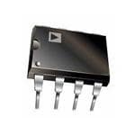
| 描述 | IC OPAMP JFET 16MHZ 8DIP精密放大器 Prec 16MHz CBFET IC |
| 产品分类 | Linear - Amplifiers - Instrumentation, OP Amps, Buffer Amps集成电路 - IC |
| 品牌 | Analog Devices |
| 产品手册 | |
| 产品图片 |
|
| rohs | 否不符合限制有害物质指令(RoHS)规范要求 |
| 产品系列 | 放大器 IC,精密放大器,Analog Devices AD845JN- |
| 数据手册 | |
| 产品型号 | AD845JN |
| 产品培训模块 | http://www.digikey.cn/PTM/IndividualPTM.page?site=cn&lang=zhs&ptm=30008http://www.digikey.cn/PTM/IndividualPTM.page?site=cn&lang=zhs&ptm=26202 |
| 产品种类 | 精密放大器 |
| 供应商器件封装 | 8-PDIP |
| 共模抑制比—最小值 | 86 dB |
| 关闭 | No |
| 包装 | 管件 |
| 压摆率 | 100 V/µs |
| 双重电源电压 | +/- 15 V |
| 商标 | Analog Devices |
| 增益带宽生成 | 16 MHz |
| 增益带宽积 | 16MHz |
| 安装类型 | 通孔 |
| 封装 | Tube |
| 封装/外壳 | 8-DIP(0.300",7.62mm) |
| 封装/箱体 | PDIP |
| 工作温度 | 0°C ~ 70°C |
| 工厂包装数量 | 50 |
| 放大器类型 | J-FET |
| 最大功率耗散 | 1.6 W |
| 最大双重电源电压 | +/- 18 V |
| 最大工作温度 | + 70 C |
| 最小双重电源电压 | +/- 4.75 V |
| 最小工作温度 | 0 C |
| 标准包装 | 50 |
| 电压-电源,单/双 (±) | ±4.75 V ~ 18 V |
| 电压-输入失调 | 700µV |
| 电压增益dB | 113.98 dB |
| 电流-电源 | 10mA |
| 电流-输入偏置 | 750pA |
| 电流-输出/通道 | 50mA |
| 电源类型 | Dual |
| 电路数 | 1 |
| 系列 | AD845 |
| 视频文件 | http://www.digikey.cn/classic/video.aspx?PlayerID=1364138032001&width=640&height=505&videoID=2245193153001http://www.digikey.cn/classic/video.aspx?PlayerID=1364138032001&width=640&height=505&videoID=2245193159001 |
| 转换速度 | 100 V/us |
| 输入偏压电流—最大 | 0.002 uA |
| 输入补偿电压 | 1.5 mV |
| 输出类型 | No |
| 通道数量 | 1 Channel |


- 商务部:美国ITC正式对集成电路等产品启动337调查
- 曝三星4nm工艺存在良率问题 高通将骁龙8 Gen1或转产台积电
- 太阳诱电将投资9.5亿元在常州建新厂生产MLCC 预计2023年完工
- 英特尔发布欧洲新工厂建设计划 深化IDM 2.0 战略
- 台积电先进制程称霸业界 有大客户加持明年业绩稳了
- 达到5530亿美元!SIA预计今年全球半导体销售额将创下新高
- 英特尔拟将自动驾驶子公司Mobileye上市 估值或超500亿美元
- 三星加码芯片和SET,合并消费电子和移动部门,撤换高东真等 CEO
- 三星电子宣布重大人事变动 还合并消费电子和移动部门
- 海关总署:前11个月进口集成电路产品价值2.52万亿元 增长14.8%


PDF Datasheet 数据手册内容提取
a Precision, 16 MHz CBFET Op Amp AD845 FEATURES CONNECTION DIAGRAMS Replaces Hybrid Amplifiers in Many Applications Plastic Mini-DIP (N) Package 16-Lead SOIC AC PERFORMANCE: and CERDIP (Q) Package (R-16) Package Settles to 0.01% in 350 ns 100 V/(cid:1)s Slew Rate 12.8 MHz Min Unity Gain Bandwidth 1.75 MHz Full Power Bandwidth at 20 V p-p DC PERFORMANCE: 0.25 mV Max Input Offset Voltage 5 (cid:1)V/(cid:2)C Max Offset Voltage Drift 0.5 nA Input Bias Current 250 V/mV Min Open-Loop Gain 4 (cid:1)V p-p Max Voltage Noise, 0.1 Hz to 10 Hz 94 dB Min CMRR Available in Plastic Mini-DIP, Hermetic CERDIP, and SOIC Packages. Also Available in Tape and Reel in Accordance with EIA-481A Standard GENERAL DESCRIPTION The AD845 conforms to the standard op amp pinout except The AD845 is a fast, precise, N channel JFET input, monolithic that offset nulling is to V+. The AD845J and AD845K grade operational amplifier. It is fabricated using Analog Devices’ devices are available specified to operate over the commercial complementary bipolar (CB) process. Advanced laser-wafer 0∞C to 70∞C temperature range. AD845A and AD845B trimming technology enables the very low input offset voltage devices are specified for operation over the –40∞C to +85∞C and offset voltage drift performance to be realized. This preci- industrial temperature range. The AD845S is specified to oper- sion, when coupled with a slew rate of 100 V/ms, a stable unity ate over the full military temperature range of –55∞C to +125∞C. gain bandwidth of 16 MHz, and a settling time of 350 ns to Both the industrial and military versions are available in 8-lead 0.01%—while driving a parallel load of 100 pF and 500 W— CERDIP packages. The commercial version is available in an represents a combination of features unmatched by any FET 8-lead plastic mini-DIP and 16-lead SOIC; J and S grade chips input IC amplifier. The AD845 can easily be used to upgrade are also available. many existing designs that use BiFET or FET input hybrid amplifiers and, in some cases, those which use bipolar input PRODUCT HIGHLIGHTS op amps. 1. The high slew rate, fast settling time, and dc precision of the AD845 make it ideal for high speed applications requiring The AD845 is ideal for use in applications such as active filters, 12-bit accuracy. high speed integrators, photodiode preamps, sample-and-hold amplifiers, and log amplifiers, and for buffering A/D and D/A 2. The performance of circuits using the LF400, HA2520, converters. The 250 mV max input offset voltage makes offset HA2522, HA2525, HA2620, HA2622, HA2625, 3550, nulling unnecessary in many applications. The common-mode OPA605, and LH0062 can be upgraded in most cases. rejection ratio of 110 dB over a ±10 V input voltage range 3. The AD845 is unity gain stable and internally compensated. represents exceptional performance for a JFET input high speed op amp. This, together with a minimum open-loop 4. The AD845 is specified while driving 100 pF/500 W loads. gain of 250 V/mV ensures that 12-bit performance is achieved, even in unity gain buffer circuits. REV.E Information furnished by Analog Devices is believed to be accurate and reliable. However, no responsibility is assumed by Analog Devices for its use, nor for any infringements of patents or other rights of third parties that may result from its use. No license is granted by implication or otherwise One Technology Way, P.O. Box 9106, Norwood, MA 02062-9106, U.S.A. under any patent or patent rights of Analog Devices. Trademarks and Tel: 781/329-4700 www.analog.com registered trademarks are the property of their respective owners. Fax: 781/326-8703 © 2003 Analog Devices, Inc. All rights reserved.
AD845–SPECIFICATIONS (@ 25(cid:2)C and (cid:3)15 V dc, unless otherwise noted.) AD845J/A AD845K/B AD845S Parameter Conditions Min Typ Max Min Typ Max Min Typ Max Unit INPUT OFFSET VOLTAGE1 Initial Offset 0.7 1.5 0.1 0.25 0.25 1.0 mV T to T 2.5 0.4 2.0 mV MIN MAX Offset Drift 20 1.5 5.0 10 mV/∞C INPUT BIAS CURRENT2 Initial V = 0 V 0.75 2 0.5 1 0.75 2 nA CM T to T 45/75 18/38 500 nA MIN MAX INPUT OFFSET CURRENT Initial V = 0 V 25 300 15 100 25 300 pA CM T to T 3/6.5 1.2/2.6 20 nA MIN MAX INPUT CHARACTERISTICS Input Resistance 1011 1011 1011 kW Input Capacitance 4.0 4.0 4.0 pF INPUT VOLTAGE RANGE Differential ±20 ±20 ±20 V Common-Mode (cid:3)10 +10.5/–13 (cid:3)10 +10.5/–13 (cid:3)10 +10.5/–13 V Common-Mode Rejection VCM = ±10 V 86 110 94 113 86 110 dB INPUT VOLTAGE NOISE 0.1 Hz to 10 Hz 4 4 4 mV p-p f = 10 Hz 80 80 80 nV/÷Hz f = 100 Hz 60 60 60 nV/÷Hz f = 1 kHz 25 25 25 nV/÷Hz f = 10 kHz 18 18 18 nV/÷Hz f = 100 kHz 12 12 12 nV/÷Hz INPUT CURRENT NOISE f = 1 kHz 0.1 0.1 0.1 pA/÷Hz OPEN-LOOP GAIN VO = ±10 V RLOAD ≥ 2 kW 200 500 250 500 200 500 V/mV RLOAD ≥ 500 W 100 250 125 250 100 250 V/mV T –T 70 75 50 V/mV MIN MAX OUTPUT CHARACTERISTICS Voltage RLOAD ≥ 500 W (cid:3)12.5 (cid:3)12.5 (cid:3)12.5 V Current Short Circuit 50 50 50 mA Output Resistance Open Loop 5 5 5 W FREQUENCY RESPONSE Small Signal Unity Gain 12.8 16 13.6 16 13.6 16 MHz Full Power Bandwidth3 VO = ±10 V RLOAD = 500 W 1.75 1.75 1.75 MHz Rise Time 20 20 20 ns Overshoot 20 20 20 % Slew Rate 80 100 94 100 94 100 V/ms Settling Time 10 V Step C = 100 pF LOAD RLOAD = 500 W to 0.01% 350 350 500 350 500 ns to 0.1% 250 250 250 ns DIFFERENTIAL GAIN f = 4.4 MHz 0.04 0.04 0.04 % DIFFERENTIAL PHASE f = 4.4 MHz 0.02 0.02 0.02 Degree POWER SUPPLY Rated Performance ±15 ±15 ±15 V Operating Range (cid:3)4.75 (cid:3)18 (cid:3)4.75 (cid:3)18 (cid:3)4.75 (cid:3)18 V Rejection Ratio VS = ±5 to ±15 V 88 110 95 113 88 110 dB Quiescent Current T to T 10 12 10 12 10 12 mA MIN MAX NOTES 1Input offset voltage specifications are guaranteed after five minutes of operation at TA = 25∞C. 2Bias current specifications are guaranteed maximum at either input after five minutes of operation at TA = 25∞C. 3FPBW = slew rate/2 p V peak. 4S grade TMIN–TMAX are tested with automatic test equipment at TA = –55∞C and TA = +125∞C. All min and max specifications are guaranteed. Specifications shown in boldface are tested on all production units at final electrical test. Results from these tests are used to calculate outgoing quality levels. Specifications subject to change without notice. –2– REV. E
AD845 ABSOLUTE MAXIMUM RATINGS1 METALIZATION PHOTOGRAPH Supply Voltage . . . . . . . . . . . . . . . . . . . . . . . . . . . . . . . . ±18 V Dimensions shown in inches and (mm). Internal Power Dissipation2 Contact factory for latest dimensions. Plastic Mini-DIP . . . . . . . . . . . . . . . . . . . . . . . . . . . . .1.6 W CERDIP . . . . . . . . . . . . . . . . . . . . . . . . . . . . . . . . . . .1.4 W 16-Lead SOIC . . . . . . . . . . . . . . . . . . . . . . . . . . . . . . .1.5 W Input Voltage . . . . . . . . . . . . . . . . . . . . . . . . . . . . . . . . . . .+V S Output Short-Circuit Duration . . . . . . . . . . . . . . . . Indefinite Differential Input Voltage . . . . . . . . . . . . . . . . . .+V and –V S S Storage Temperature Range Q . . . . . . . . . . . . . . . . . . . . . . . . . . . . . . . .–65∞C to +150∞C N, R . . . . . . . . . . . . . . . . . . . . . . . . . . . . . .–65∞C to +125∞C Lead Temperature Range (Soldering 60 sec) . . . . . . . . . 300∞C NOTES 1Stresses above those listed under Absolute Maximum Ratings may cause perma- nent damage to the device. This is a stress rating only, and functional operation of the device at these or any other conditions above those indicated in the operational sections of this specification is not implied. Exposure to absolute maximum rating conditions for extended periods may affect device reliability. 2Mini-DIP package: qJA = 100∞C/W; CERDIP package: qJA = 110∞C/W; SOIC SUBSTRATE CONNECTED TO +VS package: qJA = 100∞C/W. ORDERING GUIDE Temperature Package Package Model Range Description Option1 AD845JN 0∞C to 70∞C 8-Lead PDIP N-8 AD845KN 0∞C to 70∞C 8-Lead PDIP N-8 AD845JR-16 0∞C to 70∞C 16-Lead SOIC R-16 AD845JR-16-REEL 0∞C to 70∞C Tape and Reel R-16 AD845JR-16-REEL7 0∞C to 70∞C Tape and Reel R-16 AD845AQ –40∞C to +85∞C 8-Lead CERDIP Q-8 AD845BQ –40∞C to +85∞C 8-Lead CERDIP Q-8 AD845SQ –55∞C to +125∞C 8-Lead CERDIP Q-8 AD845SQ/883B –55∞C to +125∞C 8-Lead CERDIP Q-8 5962-8964501PA2 –55∞C to +125∞C 8-Lead CERDIP Q-8 AD845JCHIPS 0∞C to 70∞C Die NOTES 1N = Plastic DIP; Q = CERDIP; R = Small Outline IC (SOIC). 2See military data sheet. REV. E –3–
AD845–Typical Performance Characteristics TPC 1.Input Voltage Swing TPC 2.Output Voltage Swing TPC 3.Output Voltage Swing vs. Supply Voltage vs. Supply Voltage vs. Resistive Load TPC 4.Quiescent Current vs. TPC 5.Input Bias Current vs. TPC 6.Magnitude of Output Supply Voltage Temperature Impedance vs. Frequency TPC 7.Input Bias Current vs. TPC 8.Short-Circuit Current TPC 9.Unity-Gain Bandwidth Common-Mode Voltage Limit vs. Temperature vs. Temperature –4– REV. E
AD845 TPC 10.Open-Loop Gain and TPC 11.Open-Loop Gain vs. TPC 12.Power Supply Phase Margin vs. Frequency Supply Voltage Rejection vs. Frequency TPC 13.Common-Mode TPC 14.Large Signal Frequency TPC 15. Output Swing and Rejection vs. Frequency Response Error vs. Settling Time TPC 16.Harmonic Distortion TPC 17.Input Noise Voltage TPC 18.Slew Rate vs. Temperature vs. Frequency Spectral Density REV. E –5–
AD845 TPC 19.Recommended Power TPC 20.AD845 Simplified TPC 21.Offset Null Configuration Supply Bypassing Schematic TPC 22.Unity Gain Follower TPC 23. Unity Gain Follower TPC 24.Unity Gain Follower Large Signal Pulse Response Small Signal Pulse Response TPC 25.Unity Gain Inverter TPC 26.Unity Gain Inverter TPC 27.Unity Gain Inverter Large Signal Pulse Response Small Signal Pulse Response –6– REV. E
AD845 MEASURING AD845 SETTLING TIME stable, accurately defined gain. Low input bias currents and fast Figure 1 shows AD845 settling time performance. This measure- settling are achieved with the FET input AD845. ment was accomplished by driving the amplifier in the unity Most monolithic instrumentation amplifiers do not have the gain inverting mode with a fast pulse generator. The input high frequency performance of the circuit in Figure 3. The cir- summing junction was measured using false nulling techniques. cuit bandwidth is 10.9 MHz at a gain of 1 and 8.8 MHz at a Settling time is defined as the interval of time from the application gain of 10; settling time for the entire circuit is 900 ns to 0.01% of an ideal step function input until the closed-loop amplifier for a 10 V step (Gain = 10). output has entered and remains within a specified error band. The capacitors employed in this circuit greatly improve the Components of settling time include: amplifier’s settling time and phase margin. 1. Propagation time through the amplifier 2. Slewing time to approach the final output value 3. Recovery time from overload associated with the slewing 4. Linear settling to within a specified error band These individual components can be seen easily in Figure 1. Settling time is extremely important in high speed applications where the current output of a DAC must be converted to a voltage. When driving a 500 W load in parallel with a 100 pF capacitor, the AD845 settles to 0.1% in 250 ns and to 0.01% in 310 ns. Figure 3.High Performance, High Speed Instrumentation Amplifier Table I. Performance Summary for the 3-Op Amp Instrumentation Amplifier Circuit 3-Op Amp In-Amp Figure 1.Settling Characteristics 0 V to 10 V Step Small Signal Settling Time Upper Trace: Output of AD845 Under Test (5 V/Div) Gain R Bandwidth to 0.01% G Lower Trace: Error Voltage (1 mV/Div) 1 Open 10.9 MHz 500 ns 2 2 kW 8.8 MHz 500 ns 10 226 W 2.6 MHz 900 ns 100 20 W 290 kHz 7.5 ms Note: Resistors around the amplifiers’ input pins need to be small enough in value so that the RC time constant they form, with stray circuit capacitance, does not reduce circuit bandwidth. Figure 2.Settling Time Test Circuit A HIGH SPEED INSTRUMENTATION AMP The 3-op amp instrumentation amplifier circuit shown in Figure 3 can provide a range of gains from unity up to 1000 and Figure 4.The Pulse Response of the 3-Op Amp higher. The instrumentation amplifier configuration features Instrumentation Amplifier. Gain = 1, Horizontal Scale = high common-mode rejection, balanced differential inputs, and 0.5 ms/Div and Vertical Scale = 5 V/Div. REV. E –7–
AD845 Figure 5.Settling Time of the 3-Op Amp Instrumentation Figure 6. Settling Time of the Three Op Amp Instru- Amplifier. Horizontal Scale is 200 ns/Div, Vertical Scale, mentation Amplifier. Horizontal Scale: 200 ns/Div; Vertical Positive Pulse Input is 5 V/Div and Output Settling is Scale, Negative Pulse Input: 5 V/ Div; Output Settling: 1 mV/Div. 1 mV/Div. DRIVING THE ANALOG INPUT OF AN A/D CONVERTER AD845 is ideally suited to drive high resolution A/D converters An op amp driving the analog input of an A/D converter, such with 5 ms or longer conversion times since it offers both wide as that shown in Figure 7, must be capable of maintaining a bandwidth and high open-loop gain. constant output voltage under dynamically changing load condi- tions. In successive approximation converters, the input current is compared to a series of switched trial currents. The compari- son point is diode clamped but may deviate several hundred millivolts, resulting in high frequency modulation of A/D input current. The output impedance of a feedback amplifier is made artificially low by the loop gain. At high frequencies, where the loop gain is low, the amplifier output impedance can approach its open-loop value. Most IC amplifiers exhibit a minimum open-loop output impedance of 25 W due to current limiting resistors. A few hundred microamps reflected from the change in converter loading can introduce errors in instantaneous input voltage. If the A/D conversion speed is not excessive and the bandwidth of the amplifier is sufficient, the amplifier’s output will return to the nominal value before the converter makes its comparison. However, many amplifiers have relatively narrow bandwidth, yielding slow recovery from output transients. The Figure 7.AD845 As ADC Unity Gain Buffer –8– REV. E
AD845 OUTLINE DIMENSIONS 8-Lead Plastic Dual In-Line Package [PDIP] 16-Lead Standard Small Outline Package [SOIC] (N-8) Wide Body Dimensions shown in inches and (millimeters) (R-16) Dimensions shown in millimeters and (inches) 0.375 (9.53) 0.365 (9.27) 10.50 (0.4134) 0.355 (9.02) 10.10 (0.3976) 8 5 0.295 (7.49) 16 9 0.285 (7.24) 7.60 (0.2992) 1 4 0.275 (6.98) 7.40 (0.2913) 0.325 (8.26) 0.310 (7.87) 10.65 (0.4193) 0.100 (2.54) 0.300 (7.62) 0.150 (3.81) 1 8 10.00 (0.3937) BSC 0.135 (3.43) 0.180 0.015 0.120 (3.05) (4M.5A7X) (M0I.N38) 1.27B (0S.C0500) 2.65 (0.1043) 0.75 (0.0295)(cid:4) 45(cid:2) 0.015 (0.38) 2.35 (0.0925) 0.25 (0.0098) 0.30 (0.0118) 0.150 (3.81) SEATING 0.010 (0.25) 0.10 (0.0039) 0.130 (3.30) PLANE 0.008 (0.20) 000.1..00121028 ( 2((00.7..54966))) 000...000654005 (((111...521274))) COPL0A.1N0ARITY 00..5311 ((00..00210212)) SPELAANTIENG 00..3230 ((00..00103709)) 08(cid:2)(cid:2) 10..2470 ((00..00510507)) 0.014 (0.36) COMPLIANT TO JEDEC STANDARDS MS-013AA CONTROLLING DIMENSIONS ARE IN MILLIMETERS; INCH DIMENSIONS COMPLIANT TO JEDEC STANDARDS MO-095AA (IN PARENTHESES) ARE ROUNDED-OFF MILLIMETER EQUIVALENTS FOR CONTROLLING DIMENSIONS ARE IN INCHES; MILLIMETER DIMENSIONS REFERENCE ONLY AND ARE NOT APPROPRIATE FOR USE IN DESIGN (IN PARENTHESES) ARE ROUNDED-OFF INCH EQUIVALENTS FOR REFERENCE ONLY AND ARE NOT APPROPRIATE FOR USE IN DESIGN 8-Lead Ceramic Dual In-Line Package [CERDIP] (Q-8) Dimensions shown in inches and (millimeters) 0.005 (0.13) 0.055 (1.40) MIN MAX 8 5 0.310 (7.87) PIN 1 0.220 (5.59) 1 4 0.100 (2.54) BSC 0.405 (10.29) MAX 0.320 (8.13) 0.290 (7.37) 0.060 (1.52) 0.200 (5.08) 0.015 (0.38) MAX 0.200 (5.08) 0.150 (3.81) 0.125 (3.18) MIN 0.023 (0.58) SEATING 0.015 (0.38) 0.014 (0.36) 00..007300 ((10..7786)) PLANE 1 05 0.008 (0.20) CONTROLLING DIMENSIONS ARE IN INCHES; MILLIMETERS DIMENSIONS (IN PARENTHESES) ARE ROUNDED-OFF INCH EQUIVALENTS FOR REFERENCE ONLY AND ARE NOT APPROPRIATE FOR USE IN DESIGN REV. E –9–
AD845 Revision History Location Page 10/03—Data Sheet changed from REV. D to REV. E. Renumbered figures and TPCs . . . . . . . . . . . . . . . . . . . . . . . . . . . . . . . . . . . . . . . . . . . . . . . . . . . . . . . . . . . . . . . . . . . . . . .Universal Updated OUTLINE DIMENSIONS . . . . . . . . . . . . . . . . . . . . . . . . . . . . . . . . . . . . . . . . . . . . . . . . . . . . . . . . . . . . . . . . . . . . . . . .9 –10– REV. E
–11–
E) 3( 0 0/ 1 – 0 – 6 8 8 0 0 C –12–
Mouser Electronics Authorized Distributor Click to View Pricing, Inventory, Delivery & Lifecycle Information: A nalog Devices Inc.: AD845JN AD845JRZ-16 5962-8964501PA AD845SQ/883B AD845KNZ AD845JRZ-16-REEL7 AD845BQ AD845JRZ-16-REEL AD845SQ AD845JNZ AD845AQ