ICGOO在线商城 > 传感器,变送器 > 运动传感器 - 振动 > V21BL
 Datasheet下载
- 型号: V21BL
- 制造商: Mide Technology Corporation
- 库位|库存: xxxx|xxxx
- 要求:
| 数量阶梯 | 香港交货 | 国内含税 |
| +xxxx | $xxxx | ¥xxxx |
查看当月历史价格
查看今年历史价格
V21BL产品简介:
ICGOO电子元器件商城为您提供V21BL由Mide Technology Corporation设计生产,在icgoo商城现货销售,并且可以通过原厂、代理商等渠道进行代购。 V21BL价格参考。Mide Technology CorporationV21BL封装/规格:运动传感器 - 振动, Acceleration Sensor Analog Through Hole PC Pins。您可以下载V21BL参考资料、Datasheet数据手册功能说明书,资料中有V21BL 详细功能的应用电路图电压和使用方法及教程。
Mide Technology Corporation的V21BL型号属于运动传感器 - 振动类别,是一款高性能压电振动传感器。其应用场景广泛,主要适用于以下领域:

1. 工业设备监测:用于监控旋转机械(如电机、泵、压缩机等)的振动状态,帮助预测设备故障和优化维护计划。

2. 结构健康监测:可用于桥梁、建筑、风力发电机塔架等大型结构的振动监测,评估结构完整性及安全性能。

3. 汽车工业:在车辆测试中用于测量发动机、变速箱及其他部件的振动特性,提升设计质量和驾驶体验。

4. 航空航天:应用于飞机引擎、起落架和其他关键部件的振动检测,确保飞行安全与可靠性。

5. 消费电子:集成到智能设备中以实现手势识别或冲击检测等功能,提高用户体验。

6. 科研实验:为实验室提供精确的振动数据采集,支持声学、材料科学等领域研究。

V21BL凭借其高灵敏度、宽频率范围和坚固耐用的设计,在需要精准振动测量的各种环境中表现出色。
| 参数 | 数值 |
| 产品目录 | |
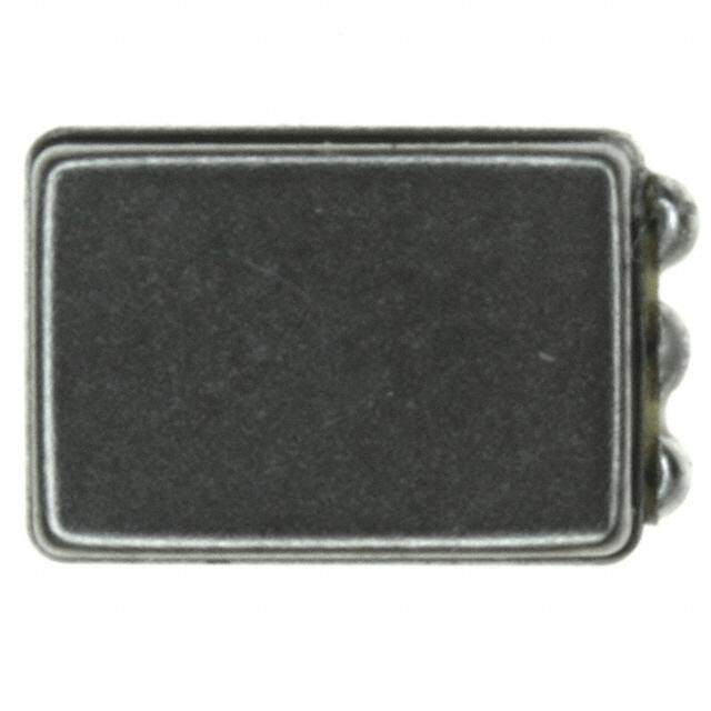
| 描述 | PIEZOELECTRIC ENERGY HARVESTER |
| 产品分类 | 震动传感器 |
| 品牌 | Mide Technology Corporation |
| 数据手册 | |
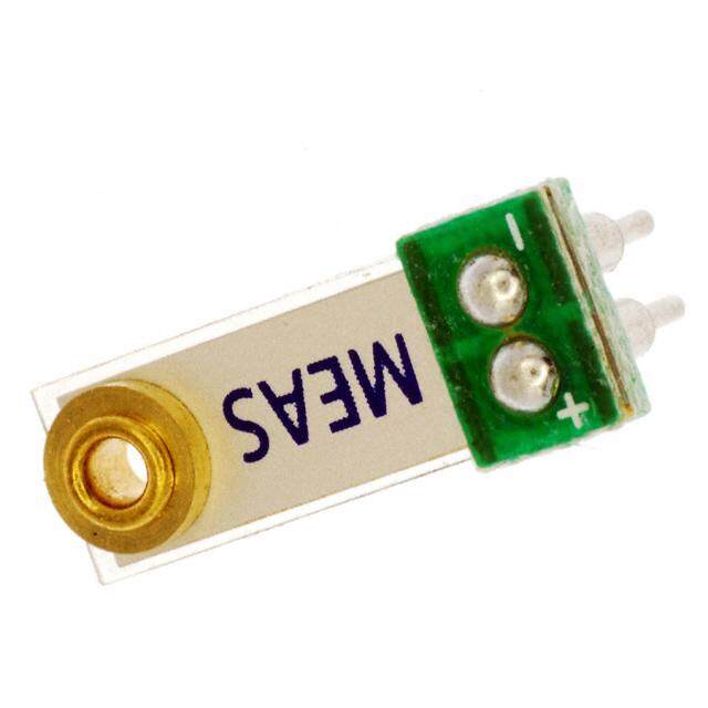
| 产品图片 |
|
| 产品型号 | V21BL |
| rohs | 含铅 / 不符合限制有害物质指令(RoHS)规范要求 |
| 产品系列 | Volture™ |
| 产品培训模块 | http://www.digikey.cn/PTM/IndividualPTM.page?site=cn&lang=zhs&ptm=25328http://www.digikey.cn/PTM/IndividualPTM.page?site=cn&lang=zhs&ptm=25691 |
| 传感器类型 | 加速 |
| 功率-额定值 | - |
| 安装类型 | 通孔 |
| 封装/外壳 | 悬臂压电薄膜(晶片) |
| 工作温度 | -40°C ~ 90°C |
| 感应范围 | 45Hz ~ 155Hz |
| 标准包装 | 1 |
| 灵敏度 | - |
| 特性 | 压电式振动能量收集,全密闭式密封 |
| 相关产品 | /product-detail/zh/VR001/VR001-ND/2402863 |
| 端接 | PC 引脚 |
| 输出类型 | 模拟 |


- 商务部:美国ITC正式对集成电路等产品启动337调查
- 曝三星4nm工艺存在良率问题 高通将骁龙8 Gen1或转产台积电
- 太阳诱电将投资9.5亿元在常州建新厂生产MLCC 预计2023年完工
- 英特尔发布欧洲新工厂建设计划 深化IDM 2.0 战略
- 台积电先进制程称霸业界 有大客户加持明年业绩稳了
- 达到5530亿美元!SIA预计今年全球半导体销售额将创下新高
- 英特尔拟将自动驾驶子公司Mobileye上市 估值或超500亿美元
- 三星加码芯片和SET,合并消费电子和移动部门,撤换高东真等 CEO
- 三星电子宣布重大人事变动 还合并消费电子和移动部门
- 海关总署:前11个月进口集成电路产品价值2.52万亿元 增长14.8%

PDF Datasheet 数据手册内容提取
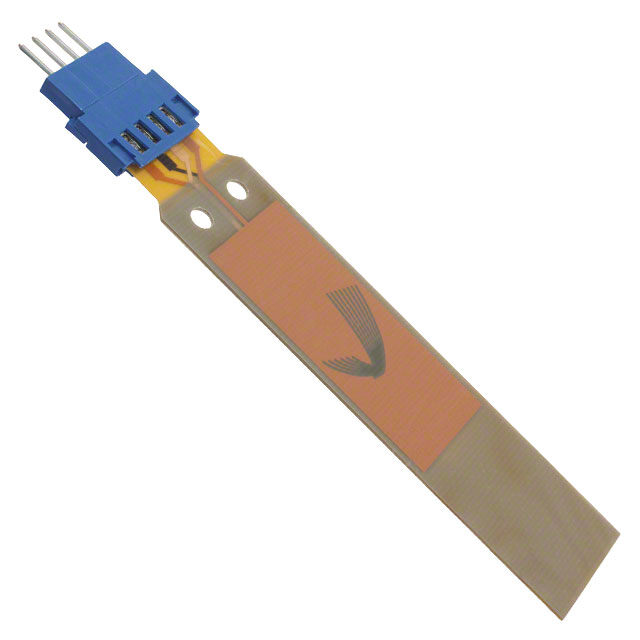
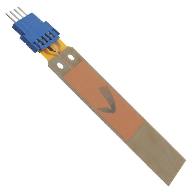
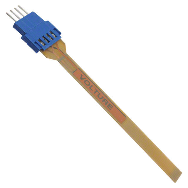
PIEZOELECTRIC ENERGY HARVESTERS FEATURES DESCRIPTION (cid:2) Enables Vibration Energy Harvesting Volture™ vibration energy harvesters convert otherwise (cid:2) Robust Piezo Packaging wasted energy from mechanical vibrations into useable electrical energy. The Volture™ accomplishes this by (cid:2) Pre-Attached Electrical Lead Wires and Connector utilizing normally brittle piezoelectric materials. The (cid:2) Hermetically Sealed for Use in Harsh Environments Midé Volture™ energy harvester is unique amongst (cid:2) Low Profile other piezo based energy harvesters because it (cid:2) Available in Different Sizes to Match to Application incorporates Midé's patented piezoelectric transducer packaging technology. (cid:2) Directly Integrate with COTS Products Such As The Linear LTC3588 and Thin Film Batteries Through a proprietary manufacturing process, the Volture™ packages piezoelectric materials in a protective skin with pre-attached electrical leads, APPLICATIONS producing a robust component with no soldered wires. The Volture’s™ protective skin also provides electrical (cid:2) Industrial Health Monitoring Network Sensors insulation and defense against humidity and harsh (cid:2) Condition Based Maintenance Sensors contaminants. (cid:2) Wireless HVAC Sensors (cid:2) Mobile Asset Tracking The Volture™ is available in six standard sizes. Custom sizes are available and a cost effective alternative. (cid:2) Tire Pressure Sensors (cid:2) Oil and Gas Sensors If a custom size is required please contact Midé (cid:2) All Air, Land and Sea Vehicle Sensors Technology Corporation by emailing: (cid:2) Battery and Hard Wired Power Replacement volture@mide.com. TYPICAL APPLICATION CHARGE VCC MANAGEMENT VIN OUT GND VSTORE MICRO TX/RX CONTROLLER SENSOR SENSOR SENSOR 1 REVISION N0. 002 REVISION DATE: 01-23-2013
PRODUCT DIMENSIONS 3.190 NOTE: 2.940 1.115 1.All dimensions are in inches CLAMP LINE .865 2.Connector thickness = 0.100” .690 Typical .250 Product Thickness (in) V20W .600 1.31 V20W 0.034 1.250 V25W 1.500 V25W 0.024 .100 V21B 0.031 1.81 2 X .129 V21BL 0.031 V22B 0.031 2.720 V22BL 0.031 2.470 1.085 CLAMP LINE .910 .300 .570 .175 .600 .660 V21B .100 1.400 2 X .110 3.560 3.310 1.085 CLAMP LINE .910 .300 .570 .175 .600 .660 V21BL .100 1.400 2 X .110 2.533 2.283 1.290 CLAMP LINE .883 .240 .600 V22B .150 1.000 .100 3.633 3.383 1.290 CLAMP LINE .883 .240 .600 V22BL .150 1.000 .100 2 REVISION N0. 002 REVISION DATE: 01-23-2013
ABSOLUTE MAXIMUM RATINGS Operating Temperature Range -40 to 90 C Operating Temperature Range (Without Connector) -40 to 150 C Storage Temperature Range -60 to 90 C Storage Temperature Range (Without Connector) -60 to 150 C Lead Temperatures (Soldering, 10 sec) 300 C Piezo Strain, max 800 micro-strain* Maximum Voltage Output Product and Vibration Dependent** Maximum Current Output Product and Vibration Dependent** **See Performance Curves For Typical Values *Related to max. tip deflection, see Deflection Limits DEFLECTION LIMITS Energy Harvester Max. Tip-to-Tip Product Number Displacement (in) V20W 0.10 V25W 0.15 TIP-TO-TIP V21B 0.06 DISPLACEMENT V21BL 0.18 FIXED TO VIBRATING SURFACE V22B 0.03 V22BL 0.12 ELECTRICAL CHARACTERISTICS Single Wafer Series Single Wafer Series Single Wafer Series Single Wafer Series Product Capacitance (nF), Resistance (Ohm), Capacitance (nF), Resistance (Ohm), measured at 100 Hz measured at 100 Hz measured at 120 Hz measured at 120 Hz V20W 69 390 69 340 V25W 130 210 130 175 V21B 26 950 26 770 V21BL 26 950 26 770 V22B 9 2400 9 2000 V22BL 9 2400 9 2000 3 REVISION N0. 002 REVISION DATE: 01-23-2013
PIN FUNCTIONS P1, P2: Piezo wafer 1 output P3, P4: Piezo wafer 2 output Series Parallel OUT 4 4 OUT 3 3 2 2 OUT 1 OUT 1 Compared to Single Wafer Value Compared to Single Wafer Value Double Voltage Same Voltage Same Current Doubled Current Capacitance: Half the Single-Wafer Value Capacitance: 2x the single-wafer value Each Volture contains two electrically isolated piezo recommended. Please refer to the connection diagram wafers, which may be used independently or bridged above. Regardless of series or parallel connection, the for increased voltage (series configuration) or current power generated by the Volture™ Energy Harvester will output (parallel configuration). Series connection will be the same. double the open-circuit voltage compared to a single wafer, and the effective capacitance will be 1/2 the In typical energy harvesting usage, the raw output is an single-wafer capacitance listed in the “Electrical AC waveform as the Volture deflects in both directions. Characteristic Table (Pg. 3)”. Parallel connection will For sensing or dual-use applications where it is desired double the current compared to a single wafer, and the to know the direction of deflection at any given time, effective capacitance will be double the single-wafer please refer to the relationship between deflection and value. For most applications, parallel connection is output polarity for each wafer diagram below. + V20W - + V25W - - V21B / BL + - + V22B / BL 4 REVISION N0. 002 REVISION DATE: 01-23-2013
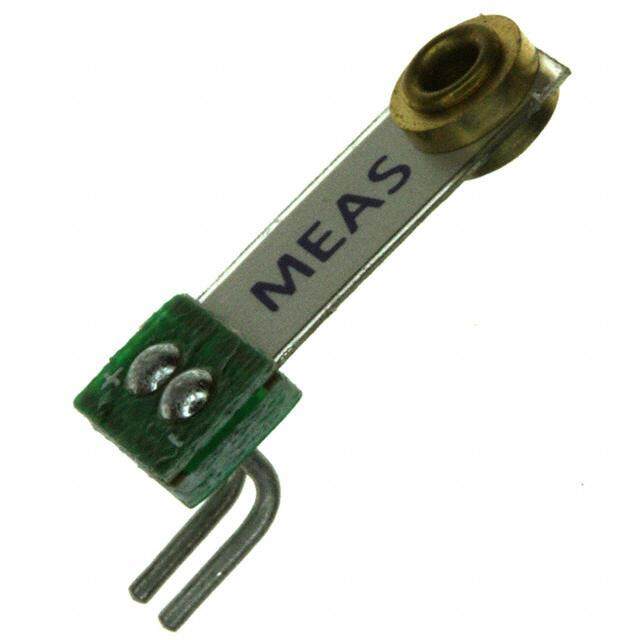
OPERATION The Volture™ vibration energy harvester is designed to provided software allows the user to easily characterize extract useable electrical energy from waste any vibration. mechanical vibrations. The best means to accomplish this is to mount the Volture™ product in a cantilevered Attaching And Clamping The Volture™ configuration on the vibration source and tune the For optimized energy harvesting from vibrations it is natural frequency of the Volture™ harvester to match best to mount the Volture™ products in a cantilevered that of the vibration source. configuration. This takes advantage of resonant beam harvesting. If the natural frequency of the Volture™ is Vibration Source Characterization successfully tuned to that of the vibration source, the The first step in successful energy harvesting is to fully most energy will be harvested. understand the vibration environment in which the Volture™ will be operating. The most effective means The first step in successful clamping is to ensure that to accomplish this is to measure the vibration using an both the base and clamp are constructed of rigid accelerometer, capture the data, and perform an FFT materials completely free of burrs and defects. Using a (Fast Fourier Transform) on the data to extract the rigid material will minimize dissipation of energy relevant frequency information. through the clamp structure and avoiding burrs and defects will minimize the potential for stress Some applications will not require this step since their concentrations on the Volture™ which could lead to dominant frequencies are inherently known. An premature failure. example of this would be a 120 Hz AC motor or a 60 Hz appliance. However, most applications will require The clamp should completely extend beyond the piezo some form of vibration characterization to be element within the Volture product. The suggested successful. clamp line shown in the product dimensions section of this document ensures that the clamp is clamping on Midé offers a vibration characterization product and the piezo element. service, the VR001. The VR001 is a small device that can be easily installed into many different vibration For long term installation, the fasteners used to secure environments. The device is completely stand alone the clamp should be properly torqued and should be and can be applied to hard to reach areas. Built in timer reinforced either using lock washers or some kind of delays allow for capture of many different types of locking adhesive. This will ensure a proper long term vibration environments. A simple USB interface with clamp that will not loosen over time. TOP VIEW TIP MASS CLAMP LINE CLAMP CONNECTOR SIDE VIEW VIBRATION BEAM SECTION FREE TO DISPLACE FIXED TO VIBRATING SURFACE 5 REVISION N0. 002 REVISION DATE: 01-23-2013
OPERATION Straight clamps are the simplest and often most cost power output. The tuning mass can then be adjusted effective clamps. However, curved clamps, as shown until the maximum power is achieved. in the diagram below, have shown the capability to slightly increase performance of the Volture. Straight If the user has a shaker available, the tuning can be clamps are sufficient for the majority of applications. performed by driving the Volture™ at the desired natural frequency and adjusting the mass until optimal Tuning The Volture™ power output is achieved. If connecting directly to the To ensure the most efficient harvesting, it is essential to Volture™ pins, optimal power output will be where the tune the Volture’s™ natural frequency to match that of voltage output is maximized. the vibrating source. Tuning is performed by adding a tuning mass to the end of the cantilevered Volture™ Another simple way to tune your Volture™ product is to measure the frequency at which the device "rings out" when excited by an impulse mechanical load. The CURVE CLAMP easiest way to perform this type of tuning is to properly mount and clamp the Volture to a rigid structure. Next, attach at least one of the piezo's within the Volture directly to an oscilloscope for monitoring (ex: connect to pins P1 and P2). Add the appropriate tip mass (See RELATION BETWEEN TIP MASS & NATURAL FREQUENCY section) to the end of the cantilevered until the natural frequency of the piezo beam is the Volture, do not permanently adhere the tip mass yet. same as the vibration source. The larger the tuning Bee's wax or tape is often the best material to use for mass the lower the natural frequency of the Volture™. non permanent tip mass installations. Apply an impulse mechanical load by very lightly "flicking" the end of the For non permanent installations or for active tuning it is Volture. This will cause the beam to "ring out". The best to use bee’s wax or some other form of non- frequency of the the decaying wave is the natural permanent attachment for the tuning mass to the frequency that the Volture is currently tuned to. To Volture. Bee’s wax allows the mass to be moved along decrease this frequency move the mass farther away the beam, toward and away from the clamp, for tuning. from the clamp point, to increase the frequency move the mass closer to the clamp point. If the natural There are multiple means of tuning the Volture™ frequency is not close to the desired frequency either a depending on the equipment available to the user. If different tip mass or a different product may be only the vibration source that will ultimately be required. harvested from is available to the user, it is recommended that the Volture™ be properly mounted Once the tip mass is in the proper location for optimal and clamped to the vibration source. The output of the energy harvesting it should be permanently adhered to Volture should then be attached to an oscilloscope for the Volture™. This ensures that the tip mass remains in monitoring. The output can be either the raw output of place for the life of the Volture™. It is recommended the Volture™ (directly on two of the output pins) or that a robust adhesive such as Loctite™ 404 be used through whatever electronics the user is using so long for this permanent installation. Keep in mind that any as the electronics allow for some measure of optimal added mass will impact the tuning of the system. 6 REVISION N0. 002 REVISION DATE: 01-23-2013
POWER MEASUREMENTS Piezoelectric material produces mechanical strain capacitance in Farads, V is the piezo’s open circuit under the influence of an externally applied electrical voltage, and Δt is a reasonable time interval (~ 10 field, and conversely produces electrical potential in seconds), and solving for C: response to applied mechanical strain. Products such 1 2 C V as the Volture™ piezo energy harvester are typically 2 P used in a cantilevered-beam configuration, in which the AVG t piezoelectric beam is clamped at one end and the other Yielding: end allowed to oscillate freely in response to vibration 2 P t AVG normal to the flat surface of the beam, converting C 2 V these vibrations to in-plane material strain. The beam dimensions and tip mass determine the resonant The figure below shows the voltage (operating voltage) frequency of the beam, which is tuned to match the on the capacitor and instantaneous power into capacitor dominant vibrational frequency of its environment, vs. time for a representative vibration level and mechanically amplifying this typically small vibration. frequency. The V25W product was used, demonstrating that the power increases until it peaks when the Power Measurements operating voltage is at about half its open circuit value. The power output capability of the Volture™ products After that, it decreases. was measured in the following manner. In the See Application Note: Load Isolation Example. cantilevered beam configuration above, the Volture was mounted to a shaker capable of generating vibrations of Typical Power & Voltage vs Time varying frequency and amplitude. Tip masses (four for each product) were added to alter the natural frequency PPEAK VOPEN CIRCUIT of the Volture™products. The vibration frequency being W) generated by the shaker was then matched to the m frequency of the Volture™ product to provide resonant wer ( and therefore optimized energy harvesting. Four os Po VOPEN CIRCUIT e n a different amplitudes were tested (0.25, 0.375, 0.5, and nt a st 1.00g) at each of these frequencies. The piezo’s output In was rectified and then placed across a purely capacitive load. The capacitor value was chosen using the 00 following equation for average power, where C is the Time (Seconds) 7 REVISION N0. 002 REVISION DATE: 01-23-2013
V20W TYPICAL PERFORMANCE POWER CHARACTERISTICS Tuned to 180 Hz | 0 gram Tip Mass Tuned to 130 Hz | 2.4 gram Tip Mass 1.8 3 0.250 g, Pmax=0.159 mW 0.250 g, Pmax=0.272 mW 1.6 0.375 g, Pmax=0.328 mW 0.375 g, Pmax=0.573 mW 0.500 g, Pmax=0.606 mW 2.5 0.500 g, Pmax=0.883 mW 1.4 1.000 g, Pmax=1.719 mW 1.000 g, Pmax=2.692 mW 1.2 2 W) 1 W) 1.5 m m er ( 0.8 er ( Pow 0.6 Pow 1 0.4 0.5 0.2 0 0 -0.2 -0.5 -2 0 2 4 6 8 10 12 -2 0 2 4 6 8 10 12 14 16 Operating Voltage Operating Voltage Tuned to 95 Hz | 7.8 gram Tip Mass Tuned to 75 Hz | 15.6 gram Tip Mass 3.5 6 0.250 g, Pmax=0.532 mW 0.250 g, Pmax=0.717 mW 0.375 g, Pmax=0.969 mW 0.375 g, Pmax=1.470 mW 3 0.500 g, Pmax=1.428 mW 5 0.500 g, Pmax=2.394 mW 1.000 g, Pmax=3.005 mW 1.000 g, Pmax=5.860 mW 2.5 4 2 W) W) 3 m m er ( 1.5 er ( ow ow 2 P 1 P 1 0.5 0 0 -0.5 -1 -2 0 2 4 6 8 10 12 14 16 18 -5 0 5 10 15 20 25 30 Operating Voltage Operating Voltage V20W RELATION BETWEEN TIP MASS & NATURAL FREQUENCY 160 Tip Mass Fn Amplitude Open Circuit 150 (gram) (Hz) (g) Voltage* 0 180 0.25 4.7 140 0 180 0.375 6.5 Hertz)130 00 118800 01.5 172..78 cy (120 2.4 130 0.25 6.7 n ue110 2.4 130 0.375 9 eq 2.4 130 0.5 11 al Fr100 2.4 130 1 18 atur 90 7.8 95 0.25 8.3 N 7.8 95 0.375 11.8 80 7.8 95 0.5 16.4 7.8 95 1 23.1 70 15.6 75 0.25 13.3 60 15.6 75 0.375 19 0 2 4 6 8 10 12 14 16 15.6 75 0.5 22.6 Tip Mass (grams) 15.6 75 1 34.7 * piezo wafers connected in series 8 REVISION N0. 002 REVISION DATE: 01-23-2013
V25W TYPICAL PERFORMANCE POWER CHARACTERISTICS Tuned to 120 Hz | 0 gram Tip Mass Tuned to 75 Hz | 2.4 gram Tip Mass 1.6 2.5 0.250 g, Pmax=0.123 mW 0.250 g, Pmax=0.134 mW 1.4 0.375 g, Pmax=0.276 mW 0.375 g, Pmax=0.292 mW 0.500 g, Pmax=0.471 mW 0.500 g, Pmax=0.513 mW 2 1.000 g, Pmax=1.468 mW 1.000 g, Pmax=2.431 mW 1.2 1 1.5 W) W) m 0.8 m er ( er ( 1 w 0.6 w o o P P 0.4 0.5 0.2 0 0 -0.2 -0.5 -2 0 2 4 6 8 10 12 -2 0 2 4 6 8 10 12 14 16 18 Operating Voltage Operating Voltage Tuned to 50 Hz | 7.8 gram Tip Mass Tuned to 40 Hz | 15.6 gram Tip Mass 8 10 0.250 g, Pmax=0.590 mW 0.250 g, Pmax=0.931 mW 7 0.375 g, Pmax=1.194 mW 0.375 g, Pmax=1.763 mW 0.500 g, Pmax=2.075 mW 0.500 g, Pmax=2.972 mW 8 1.000 g, Pmax=7.220 mW 1.000 g, Pmax=9.231 mW 6 5 6 W) W) m 4 m er ( er ( 4 w 3 w o o P P 2 2 1 0 0 -1 -2 0 5 10 15 20 25 -5 0 5 10 15 20 25 30 Operating Voltage Operating Voltage V25W RELATION BETWEEN TIP MASS & NATURAL FREQUENCY 130 Tip Mass Fn Amplitude Open Circuit (gram) (Hz) (g) Voltage* 120 0 120 0.25 3.2 110 0 120 0.375 4.4 cy (Hertz)100 002.4 11227005 010..255 1504...517 n ue 90 2.4 75 0.375 6.5 eq 2.4 75 0.5 7.5 Fr al 80 2.4 75 1 11.5 atur 7.8 50 0.25 10.3 N 70 7.8 50 0.375 15.4 7.8 50 0.5 18.6 60 7.8 50 1 29.5 15.6 40 0.25 14.5 50 15.6 40 0.375 21.2 0 1 2 3 4 5 6 7 8 15.6 40 0.5 27 Tip Mass (grams) 15.6 40 1 36.6 * piezo wafers connected in series 9 REVISION N0. 002 REVISION DATE: 01-23-2013
V21B TYPICAL PERFORMANCE POWER CHARACTERISTICS Tuned to 275 Hz | 0 gram Tip Mass Tuned to 175 Hz | 1 gram Tip Mass 0.3 0.7 0.250 g, Pmax=0.010 mW 0.250 g, Pmax=0.049 mW 0.375 g, Pmax=0.030 mW 0.375 g, Pmax=0.108 mW 0.25 0.500 g, Pmax=0.061 mW 0.6 0.500 g, Pmax=0.188 mW 1.000 g, Pmax=0.250 mW 1.000 g, Pmax=0.658 mW 0.5 0.2 0.4 W)0.15 W) m m er ( er ( 0.3 ow 0.1 ow P P 0.2 0.05 0.1 0 0 -0.05 -0.1 -1 0 1 2 3 4 5 6 7 -2 0 2 4 6 8 10 12 Operating Voltage Operating Voltage Tuned to 140 Hz | 2.4 gram Tip Mass Tuned to 105 Hz | 4.8 gram Tip Mass 1.4 2.5 0.250 g, Pmax=0.114 mW 0.250 g, Pmax=0.262 mW 0.375 g, Pmax=0.248 mW 0.375 g, Pmax=0.475 mW 1.2 0.500 g, Pmax=0.379 mW 0.500 g, Pmax=0.795 mW 2 1.000 g, Pmax=1.311 mW 1.000 g, Pmax=2.252 mW 1 1.5 0.8 W) W) m m er ( 0.6 er ( 1 w w o o P 0.4 P 0.5 0.2 0 0 -0.2 -0.5 -2 0 2 4 6 8 10 12 14 16 18 -5 0 5 10 15 20 25 Operating Voltage Operating Voltage V21B RELATION BETWEEN TIP MASS & NATURAL FREQUENCY 260 Tip Mass Fn Amplitude Open Circuit 240 (gram) (Hz) (g) Voltage* 0 275 0.25 4.1 220 0 275 0.375 5.9 Hertz) 200 00 227755 01.5 172..63 ncy ( 180 1 175 0.25 7.6 ue 1 175 0.375 10.9 eq 160 1 175 0.5 13.6 Fr al 1 175 1 23.5 atur 140 2.4 140 0.25 10.9 N 2.4 140 0.375 15.2 120 2.4 140 0.5 18.8 100 2.4 140 1 32 4.8 105 0.25 15.9 80 4.8 105 0.375 21.6 0 1 2 3 4 5 4.8 105 0.5 28.1 Tip Mass (grams) 4.8 105 1 46.5 * piezo wafers connected in series 10 REVISION N0. 002 REVISION DATE: 01-23-2013
V21BL TYPICAL PERFORMANCE POWER CHARACTERISTICS Tuned to 110 Hz | 0 gram Tip Mass Tuned to 65 Hz | 1 gram Tip Mass 0.3 0.6 0.250 g, Pmax=0.030 mW 0.250 g, Pmax=0.036 mW 0.375 g, Pmax=0.066 mW 0.375 g, Pmax=0.085 mW 0.25 0.500 g, Pmax=0.102 mW 0.5 0.500 g, Pmax=0.136 mW 1.000 g, Pmax=0.262 mW 1.000 g, Pmax=0.513 mW 0.2 0.4 W)0.15 W) 0.3 m m er ( er ( ow 0.1 ow 0.2 P P 0.05 0.1 0 0 -0.05 -0.1 -1 0 1 2 3 4 5 6 7 8 9 -2 0 2 4 6 8 10 12 14 Operating Voltage Operating Voltage Tuned to 50 Hz | 2.4 gram Tip Mass Tuned to 40 Hz | 4.8 gram Tip Mass 1.6 3 0.250 g, Pmax=0.157 mW 0.250 g, Pmax=0.263 mW 1.4 0.375 g, Pmax=0.323 mW 0.375 g, Pmax=0.549 mW 0.500 g, Pmax=0.525 mW 2.5 0.500 g, Pmax=0.906 mW 1.000 g, Pmax=1.484 mW 1.000 g, Pmax=2.662 mW 1.2 2 1 mW) 0.8 mW) 1.5 er ( er ( ow 0.6 ow 1 P P 0.4 0.5 0.2 0 0 -0.2 -0.5 -5 0 5 10 15 20 25 -5 0 5 10 15 20 25 30 Operating Voltage Operating Voltage V21BL RELATION BETWEEN TIP MASS & NATURAL FREQUENCY 130 Tip Mass Fn Amplitude Open Circuit 120 (gram) (Hz) (g) Voltage* 0 110 0.25 3.95 110 0 110 0.375 5.35 Hertz)100 00 111100 01.5 162..61 ncy ( 90 1 65 0.25 8 ue 1 65 0.375 9.9 eq 80 1 65 0.5 12.4 Fr al 1 65 1 22.1 atur 70 2.4 50 0.25 9.8 N 2.4 50 0.375 13.7 60 2.4 50 0.5 19.1 50 2.4 50 1 27.5 4.8 40 0.25 13.2 40 4.8 40 0.375 19.2 0 1 2 3 4 5 4.8 40 0.5 25.9 Tip Mass (grams) 4.8 40 1 44.4 * piezo w afers connected in series 11 REVISION N0. 002 REVISION DATE: 01-23-2013
V22B TYPICAL PERFORMANCE POWER CHARACTERISTICS Tuned to 240 Hz | 0 gram Tip Mass Tuned to 125 Hz | 0.5 gram Tip Mass 0.06 0.14 0.25 g, Pmax= 0.00 mW 0.25 g, Pmax= 0.01 mW 0.375 g, Pmax= 0.01 mW 0.375 g, Pmax= 0.03 mW 0.05 0.5 g, Pmax= 0.01 mW 0.12 0.5 g, Pmax= 0.06 mW 1.0 g, Pmax= 0.05 mW 1.0 g, Pmax= 0.13 mW 0.1 0.04 0.08 W)0.03 W) m m er ( er (0.06 ow0.02 ow P P0.04 0.01 0.02 0 0 -0.01 -0.02 -0.5 0 0.5 1 1.5 2 2.5 3 3.5 4 0 1 2 3 4 5 6 7 8 Operating Voltage Operating Voltage Tuned to 105 Hz | 1 gram Tip Mass Tuned to 80 Hz | 2 gram Tip Mass 0.3 0.6 0.25 g, Pmax= 0.03 mW 0.25 g, Pmax= 0.07 mW 0.375 g, Pmax= 0.06 mW 0.375 g, Pmax= 0.17 mW 0.25 0.5 g, Pmax= 0.10 mW 0.5 0.5 g, Pmax= 0.27 mW 1.0 g, Pmax= 0.26 mW 1.0 g, Pmax= 0.59 mW 0.2 0.4 W)0.15 W) 0.3 m m er ( er ( ow 0.1 ow 0.2 P P 0.05 0.1 0 0 -0.05 -0.1 -2 0 2 4 6 8 10 -2 0 2 4 6 8 10 12 14 16 Operating Voltage Operating Voltage V22B RELATION BETWEEN TIP MASS & NATURAL FREQUENCY 260 Tip Mass Fn Amplitude Open Circuit 240 (gram) (Hz) (g) Voltage* 0 240 0.25 2.2 220 0 240 0.375 3.4 ertz)200 0 240 0.5 4.6 H 0 240 1 7.2 ncy (180 0.5 125 0.25 6.7 ue 0.5 125 0.375 9.3 q e160 0.5 125 0.5 11.6 Fr al 0.5 125 1 18.5 atur140 1 105 0.25 9 N 1 105 0.375 12.1 120 1 105 0.5 14.7 100 1 105 1 25.1 2 80 0.25 13 80 2 80 0.375 17.4 0 0.5 1 1.5 2 2 80 0.5 22.3 Tip Mass (grams) 2 80 1 33.4 * piezo wafers connected in series 12 REVISION N0. 002 REVISION DATE: 01-23-2013
V22BL TYPICAL PERFORMANCE POWER CHARACTERISTICS Tuned to 110 Hz | 0 gram Tip Mass Tuned to 45 Hz | 0.5 gram Tip Mass 0.3 0.8 0.25 g, Pmax= 0.02 mW 0.25 g, Pmax= 0.09 mW 0.375 g, Pmax= 0.04 mW 0.7 0.375 g, Pmax= 0.17 mW 0.25 0.5 g, Pmax= 0.07 mW 0.5 g, Pmax= 0.28 mW 1.0 g, Pmax= 0.21 mW 1.0 g, Pmax= 0.75 mW 0.6 0.2 0.5 mW)0.15 mW) 0.4 er ( er ( ow 0.1 ow 0.3 P P 0.2 0.05 0.1 0 0 -0.05 -0.1 -2 0 2 4 6 8 10 12 -5 0 5 10 15 20 25 Operating Voltage Operating Voltage Tuned to 35 Hz | 1 gram Tip Mass Tuned to 30 Hz | 2 gram Tip Mass 1.2 2 0.25 g, Pmax= 0.14 mW 0.25 g, Pmax= 0.28 mW 0.375 g, Pmax= 0.30 mW 0.375 g, Pmax= 0.48 mW 1 0.5 g, Pmax= 0.45 mW 0.5 g, Pmax= 0.77 mW 1.0 g, Pmax= 1.05 mW 1.5 1.0 g, Pmax= 1.84 mW 0.8 W) 0.6 W) 1 m m er ( er ( Pow 0.4 Pow 0.5 0.2 0 0 -0.2 -0.5 -5 0 5 10 15 20 25 30 -5 0 5 10 15 20 25 30 35 40 Operating Voltage Operating Voltage V22BL RELATION BETWEEN TIP MASS & NATURAL FREQUENCY 110 Tip Mass Fn Amplitude Open Circuit 100 (gram) (Hz) (g) Voltage* 0 110 0.25 2 90 0 110 0.375 3.1 Hertz) 80 00 111100 01.5 46..29 ncy ( 70 0.5 45 0.25 6 ue 0.5 45 0.375 8.5 Freq 60 0.5 45 0.5 11 al 0.5 45 1 17.5 atur 50 1 35 0.25 8 N 1 35 0.375 11.5 40 1 35 0.5 14 30 1 35 1 23.4 2 30 0.25 12 20 2 30 0.375 16.1 0 0.5 1 1.5 2 2 30 0.5 20.8 Tip Mass (grams) 2 30 1 31.8 * piezo wafers connected in series 13 REVISION N0. 002 REVISION DATE: 01-23-2013
APPLICATIONS INFORMATION - SWITCHED CAPACITOR BOOST CIRCUIT Switched Capacitor Boost Circuit for One- bypass capacitance to reliably start up. The circuit Shot Sensors and Low Vibration Levels can begin operating almost immediately when power It is often difficult to make use of low-voltage energy becomes available. This circuit is ideal for directly scavenging sources, such as piezo energy harvesters powering small sensors that can perform their at low vibration amplitudes, solar cells in overcast or function (e.g. record or transmit a measurement) in a indoor environments, or Seebeck devices, etc., as known amount of time and power. It could also be most microcontrollers and sensors require minimum used to extend battery life, or as a trigger source for voltages of 1.8V or greater to operate. Using these devices with their own battery/supercap power sources requires a voltage boost converter with a source. minimum start-up voltage, low start-up current requirement, and graceful handling of undervoltage and When the voltage at VIN exceeds the minimum start-up slow input voltage rise times. voltage, the IC begins pumping charge to a storage capacitor connected across the CPOUT pin. When the The circuit shown, based on the Seiko Epson S-882Z capacitor voltage reaches 2.4V, the output is enabled series charge pump IC, provides bursts of power and this voltage is applied to the load. The load is starting at approximately 2.4VDC (ending at 1.6-2 automatically disconnected when the storage capacitor VDC) from input voltages as low as approximately voltage drops below approx. 1.8V (see Figure 6). This 380mV. This IC provides boosting using small on-chip behavior allows the circuit to directly power most 3.3V switched (“flying”) capacitors, rather than inductive microcontroller circuits, with a typical operating voltage boost conversion. Thus the initial input current range of 1.8V ~ 3.6V, without exposing the circuit to requirements are reduced compared to a typical boost significant undervoltage or unfavorable voltage rise- converter, requiring only a small power-supply time conditions. S-882Z 3 VH 4 VM VIN 2 Piezo Bimorph 5 GND D1 CPOUT 1 J3 VOUT X1 VCC BAT54STA C1 U1 X2 10uF 1 QPXX_RA D2 GND C3 100uF GND GND 14 REVISION N0. 002 REVISION DATE: 01-23-2013
APPLICATIONS INFORMATION - SWITCHED CAPACITOR BOOST CIRCUIT Goals 1 C (cid:2) Allow intermittently operating circuits to be 1 V R ln o powered from extremely weak vibration sources, T V d or moderate vibration sources at frequencies sig- Equation 1: Capacitance needed for nificantly different from the energy harvester's res- a given runtime (F) onant frequency (Figure 3) (cid:2) Physically disconnect the load during periods of V T R C ln o insufficient voltage to avoid "over-the-hump" prob- d V lems of cold circuit start-up from harvested power Equation 2: Runtime for a given (cid:2) Maximize chances of success where vibration capacitance (sec.) source's characteristics (amplitude and frequency content) cannot be known in advance. 1 W C V 2 V2 2 0 Simple “One-Shot” Application Equation 3: Energy per discharge (Joules or watt-seconds) A simple usage scenario is an embedded sensor with data storage/transmission capability, which takes one W set of measurements each time it is powered up P T T (relying on the loss and subsequent re-application of c d power to start the next measurement). In this case, the Equation 4: Average Power (Watts) measurement frequency is variable and depends on the vibration amplitude. To operate the sensor directly from In the equations above, T is the runtime or discharge d the boost circuit requires: time in seconds, T is the charge time in seconds, R is c the equivalent load resistance in ohms, V is the (cid:2) Estimation (or measurement of) the run-time and 0 starting output voltage (2.4), V is the final output power consumption of your application within its voltage (1.8V or the minimum operating voltage of the voltage limits sensor, whichever is greater), and C is the capacitance (cid:2) Sizing the CP according to worst-case usage, out in Farads. Likewise, the output voltage can be modeled allowing some headroom as a simple RC time constant, V = V e-T/RC. 0 For such one-shot sensors, it is recommended to create a large load (e.g. drive an LED or GPIO pin tied Continuously-Powered Application with to ground) after completing the task in order to ensure Input-Dependent Triggering the power output cycles in high-vibration conditions. Sometimes it may be advantageous to incorporate vibration-powered battery maintenance and/or A typical microcontroller sensor application’s load triggering into a continuously-running circuit. For profile will be “bursty”, complicating the task of example, a sensor may require low-level continuous estimating the required value of CP . However, if the power to maintain a realtime clock, but measurement out load can be approximated in terms of a resistive load, tasks are only needed when a piece of machinery is the following equations can be used to estimate the known to be operating. Alternately, it may be desired to required capacitance, available runtime, energy per dynamically adjust the measurement rate based on the discharge or power stored. incoming power to maintain a given power budget. In 15 REVISION N0. 002 REVISION DATE: 01-23-2013
APPLICATIONS INFORMATION - SWITCHED CAPACITOR BOOST CIRCUIT these cases, the application can use V as an Typical Results out interrupt source in addition to power source, with a The following are measured results using the circuit rising or falling edge triggering the desired action. shown in a typical configuration. Discharge Interval vs. Acceleration Averaged Power Output vs. Acceleration Volture V20W @ 60Hz, 100uF Volture V20W @ 60Hz 103 90 80 es (s) W) 70 e between discharge cycl 110012 Average power output (u 34560000 m 20 Ti 10 100 0 0 0.1 0.2 0.3 0.4 0.5 0.6 0.7 0 0.1 0.2 0.3 0.4 0.5 0.6 0.7 Acceleration (g) Acceleration (g) Figure 2: Discharge Interval vs. Acceleration, measured Figure 4: Averaged Power Output vs. Acceleration results using configuration shown Usable Bandwidth vs. Acceleration Volture V20W 60 Hz (Hz) 50 0 6 = c 40 F at h widt 30 d n a b W 20 0 2 V e abl 10 s U 0 0.2 0.3 0.4 0.5 0.6 0.7 0.8 0.9 1 1.1 1.2 Acceleration (g) Figure 3: Usable Bandwidth vs. Acceleration at 60Hz center frequency. Usable bandwidth refers to the frequency range over which the setup produced voltages exceeding the circuit’s turn-on threshold (2.4V), producing output pulses. 16 REVISION N0. 002 REVISION DATE: 01-23-2013
APPLICATIONS INFORMATION - SWITCHED CAPACITOR BOOST CIRCUIT Tek Stop Tek Stop : 570mV : 570mV @: 2.42 V @: 2.42 V 3 3 Ch1 500mV Ch2 500mV Ch3 500mV M 2.00 s A Ch1 0.00 V Ch1 500mV Ch2 500mV Ch3 500mV M 200ms A Ch1 0.00 V Figure 5: Rectified input (aqua), V (navy) and switched Figure 6: Rectified input (aqua), V (navy) and switched CAP CAP output (violet) from initial start-up to stable output, 10K output (violet) output pulse detail, 10K resistive load. resistive load. 17 REVISION N0. 002 REVISION DATE: 01-23-2013
APPLICATIONS INFORMATION - LOAD ISOLATION EXAMPLE Load Isolation Example for Maximum Efficiency with Low-Impedance Loads R A cantilevered-beam piezoelectric energy harvester is a leak complex electromechanical system in which the electrical and mechanical loading of the beam are inter- related. Understanding of this relationship is critical to getting the most out of the system. R leak A properly tuned switched boost-buck circuit will always outperform any circuit in which you do not tune to the characteristics of its application. This application note demonstrates a high-efficiency Figure 1: Piezo parallel and series equivalent circuits switched step-down (buck) converter and optimizations for maximum performance in a real- environment. Care must be taken to choose when this world application. This circuit isolates the end- power is drawn. To maximize transfer efficiency, the application’s electrical load from the piezo beam, load must be matched to the piezo’s equivalent providing proper impedance-matching of the circuit’s impedance. In practice, the piezo impedance at a given “virtual load” to the beam, as well as minimizing amplitude and frequency, as well as the load mechanical loading effects. Such a circuit is ideal for impedance, can be thought of as a pair of simple (but low-impedance loads such as rechargeable batteries, unknown) resistances which make up a resistor “bursty” loads such as intermittently-operating divider. The power transfer between the two is sensors/transmitters, and applications where the optimized when their values match. This corresponds electrical load cannot be known in advance. to the point at which the piezo’s loaded voltage is equal to half its open-circuit voltage. Thus the impedance Basic Piezoelectric Beam Model match can be optimized without formally measuring or Before mechanical loading effects are taken into knowing the impedance of the piezo source or load in- account, each piezo beam can be thought of as a small situ. current source in parallel with a capacitor and parasitic resistance, as shown in Figure 1. Typical values for this Implementation parallel capacitance and resistance are on the order of The circuit of Figure 2 provides a simple but effective 10nF and >40M, respectively. This parallel resistance approach to meeting these goals. is insignificant for our purposes and may be ignored. The current flow is equal to the derivative of the strain- The main components are a bridge rectifier formed by induced charge, or dQ/dt. The voltage transfer function D1-D4, low-power comparator (U1) and buck of each beam therefore is V(s)/q(s) = sR/(1+sRC), converter (U2). During vibration, main storage where R is the parallel resistance and C is the parallel capacitor C1 slowly charges until its voltage reaches capacitance of the beam. the operating point (V /2) set by R1 and R2. Buck oc converter U2 is enabled once the stored voltage In its simplest form, power is drawn from a small exceeds this value plus a small hysteresis. At typical capacitor which is constantly recharged by its loads, the buck converter operation into the load will 18 REVISION N0. 002 REVISION DATE: 01-23-2013
APPLICATIONS INFORMATION - LOAD ISOLATION EXAMPLE VCC R3 15M (Optional) BAT43W XX12Piezo Bimorph BBDDAA21VV119999 Zener 11VD5 A C + 1C010uF1M5.7M R2R1 11VRC00 R24n0EFKF R2.523561ML+HRT-ICEYNINF1S54GND 0COMVUV+ST-8728 V1RC6RCUN 7638 ULVSLRT2BIEUCNINN1DS46E74CGLMVSNBFSWODB8 1254SWD7100uH VBAT43WOU+TVFB1C u3F 2.4M4.7M R7R8 V124pBDFA8T43W VGONUDT GND Figure 2: Simple high-efficiency voltage conversion and load-isolation circuit for piezo energy harvesting applications. The C1 voltage setpoint in this example is fixed, but could be made adaptive using additional circuitry. deplete C1 until its voltage drops below the hysteresis least as much power as is being supplied (Figure 5). band, at which point the converter is disabled and the The converter duty cycle is approximated by the ratio cycle repeats. Thus C1 is maintained at approximately of input power (G-level) vs. output power (voltage * V /2. The typical output is a train of voltage-regulated current * time), less any small conversion losses and oc pulses ideally suited to charging a battery or capacitor, leakage. When the input power exceeds the output and or directly powering an intermittently-operating sensor. losses, duty cycle will be 100%, and excess voltage at C1 is safely disposed of through D5. Since the voltage at C1 is held approximately constant, the effective load seen by the piezo is not significantly R6 sets the peak current through inductor L1, and can affected by activation of U2 or changes to the actual be specified according to the equation: load. Additionally, the voltage maintained on C1 ensures charge is drawn from the piezo beam only 0.067 when its voltage exceeds C1’s voltage by one diode R 0.25 SENSE I drop, which occurs only when the beam approaches its MAX maximum deflection. Thus a limited amount of charge is drawn on each cycle of the piezo beam, timed to where I is the maximum desired output current to MAX coincide with the maximum deflection of the beam. the load. Generally, the peak inductor current should be This combination of factors helps prevent excessive set to maximum to improve efficiency with smaller mechanical damping of the beam, allowing usable (<300uH) inductors in space-limited applications; output voltages to be output at lower vibration refer to the LT1474 datasheet for more thoughtful amplitudes while the piezo beam is driven near its trade-offs between peak current and inductor size. mechanical resonance. Battery-charging applications requiring a (pulsed) constant-current charge phase, or where both the U2 provides a regulated output voltage determined by charge circuit and the load are directly connected the ratio of R7 and R8. The power output per G of across the battery pack, may require a lower I PEAK vibration will remain relatively constant across G-levels setting to reduce voltage ripple caused by the charge and loads, provided the load is capable of drawing at pulses. 19 REVISION N0. 002 REVISION DATE: 01-23-2013
APPLICATIONS INFORMATION - LOAD ISOLATION EXAMPLE Considerations for Conversion Efficiency of the internal switch, current sense resistor, and Converter efficiency is defined as the output power inductor) contribute resistive losses. At low values of divided by the input power times 100%. V , switch losses will dominate, and can be minimized IN by using a suitably large inductor and low I . At PEAK The losses from the circuit’s front-end components higher supply voltages, these losses are proportional to (leakage across the storage capacitor, comparator, and load. R1-R3) will be small (uA) and largely proportional to the C1 voltage setpoint. Minimizing losses here is Catch Diode Losses straightforward by appropriate component selection of The catch diode, D7, introduces a loss (V*I) as it C1 and suitably large values of R1 – R3. These small conducts during the switch off-time, proportional to its losses will occur for the entire time that voltage is forward voltage, and more pronounced at high supply present on C1. voltage where the switch on-time is shorter. Again, V IN is fixed for piezo efficiency reasons, so this loss is best The remaining controllable losses will occur in the minimized by minimizing the diode V and converter f step-down converter section and, apart from the duty cycle. By lowering the duty cycle, a reduction in V f LT1474’s shutdown current, occur only during the ON- of the catch diode will improve efficiency even though time of the output. The main losses will come from low-V diodes tend to have much higher reverse f three sources: V current, I2Rlosses, and catch diode leakage currents, which will produce loss during the IN losses. switch ON-time. In any event, the catch diode must be sized to safely handle I at nearly 100% duty cycle PEAK V (worst-case condition; output shorted). IN The V current of the LT1474 is due to two IN components: the DC bias current and the gate charge The selection of 100uH inductor should be considered current of its internal P-channel switch. Both are a minimum, for use in conjunction with high I PEAK proportional to V ; however, at load currents > 1mA, values. Particularly in applications where space is not IN the DC bias current (from 9uA at no load to 100uA in constrained or I must be reduced, inductors as PEAK continuous mode) is negligible compared to the gate large as 1000uH may be required for maximum charge losses. Each time the gate is switched on and efficiency. The ideal range of inductor size at a given off, a packet of charge dQ moves from V to ground. I is a trade-off between the increased resistance of IN MAX In continuous mode, I = fQp where Qp is the gate higher-value inductors and the increased switching GATE charge of the internal switch and f is the switching rates required for lower-value inductors. frequency. Since V is pre-set according to piezo IN efficiency considerations, the best way to minimize this At light loads, the output duty cycle will rise and losses loss is to keep the output duty cycle low. in the conversion stage (leakage, switching and catch diode losses) will accrue. This may or may not be a Resistive (I2R) Losses problem; it could simply mean that more power is The resistances in the current path (The ON-resistance available than the load can use. 20 REVISION N0. 002 REVISION DATE: 01-23-2013
APPLICATIONS INFORMATION - LOAD ISOLATION EXAMPLE Application Example (Circuit adaptations for self-adjusting bias voltage may The steps to configure this circuit optimally for a given be explored if the power gains exceed the consumption load are presented below. This example assumes the of the added circuitry.) following are known: The LTC1540 features a programmable hysteresis (cid:2) Required output voltage band of up to 100mV. However, a larger hysteresis is generally preferable to allow for smaller values of C1 (cid:2) Required output current and/or longer output ON-times, particularly for directly- (cid:2) Nominal piezo open-circuit voltage powered sensors. This can be accomplished by 1) Set output voltage bypassing the onboard hysteresis adjustment (R4=0 The output voltage is determined by ohms; R5=open) and adding a small amount of positive feedback via R3. R7 Vout = 1.23 1+ V R8 First select the desired center voltage (Vc) for C1 and the desired hysteresis band (V ). Choose a value for hb Where V is the forward voltage drop of D8 under load. R1 such that the current across it at the trip point is f In direct sensor-power applications where reverse substantially greater than the comparator’s input leakage into the circuit during its off-time is not a leakage (1nA typ.), for example 100nA. The 5.7M value concern, D8 may be omitted (but see important shown is perfectly reasonable, but the following will warnings below). To minimize no-load supply current, more formally dictate its upper limit. The LTC1540’s resistor values in the megaohm range should be used. internal reference (Vref) is 1.182V. The current through R1 at the lower trip point is (Vc-(Vhb/2)-Vref) / R1. 2) Choose inductor size and maximum inductor Thus the upper limit for R1 is current, following the guidelines of the LT1474 V datasheet. For greatest efficiency where space is not a Vc hb 1.182 concern, first choose the inductor current sense 2 R1 resistor R6 according to desired output current I R1 (R Equation above), then size the inductor SENSE accordingly. For space-limited applications, size L1 as Choose R2 to set the center voltage, Vc. Neglecting the dictated by the available space and set I as high small influence of R3, PEAK as the inductor will tolerate without saturating. 1.182 R1 R2 3) Choose C1 bias voltage to be approximately ½ the Vc 1.182 open-circuit piezo voltage in its natural vibration environment. In applications with highly variable Choose R3 to set the hysteresis. At the lower amplitudes, a trade-off must be made between comparator trip point, the threshold voltage will be efficiency at higher amplitudes and the ability to equal to harvest power from lower amplitudes: no charge will R2 be drawn by this circuit if the piezo open-circuit voltage V L R2 R1 R3 after rectification never reaches the set turn-on voltage. 21 REVISION N0. 002 REVISION DATE: 01-23-2013
APPLICATIONS INFORMATION - LOAD ISOLATION EXAMPLE as the comparator will be ON when approaching this Latch-Up Consideration point. Solving for R3, If diode D8 is removed, the designer must pay attention to D6, which is necessary to prevent latch-up of the R1 R2 VL Vth R3 LT1474’s output switch if the voltage at its SW pin is R1 Vth R2 Vth R2 VL held up while V drops. This situation may easily IN The addition of R3 will slightly affect the actual center occur in an application where the load is powered by voltage; however, this change will typically not be multiple sources or includes a storage element, such significant in comparison with the size of the hysteresis as supercapacitor or battery, whose voltage drops band. For a typical V (>3.3V), the final value of V will more slowly than that of C1 when no harvested power c c be lowered. As indicated by Figure 5, however, driving is available. The user must then choose D6 so that the the piezo to moderately higher open-circuit voltages voltage at SW cannot exceed the voltage at V by the IN than optimal does not have an excessive impact on 0.6V required for latch-up. Particularly at high C1 efficiency. voltages, the designer must also take steps to ensure that reverse leakage over D6 will not allow the voltages Check: Actual V and V at the V and SW pins to float above their maximum h l FB Once all resistor values are chosen, the actual upper ratings at no load. and lower trip points will be defined by: R2 R3 R1 V 1.182 h R2 R3 R1 R3 R2 V 1.182 l R2 22 REVISION N0. 002 REVISION DATE: 01-23-2013
APPLICATIONS INFORMATION - POWER MANAGEMENT IC INTEGRATION Integration with LTC3588 Charge advantage of the high voltage input since the buck Management IC converter on the chip can deliver 100mA average The LTC3588-1 is an ultra low quiescent current power current efficiently to the load. The input capacitor supply designed specifically for energy harvesting should then be sized to store enough energy to provide applications. The part is designed to interface directly to output power for the length of time required, while also a piezoelectric or alternative A/C power source such as not dropping to the undervoltage lockout falling the Volture™. The part rectifies a voltage waveform and threshold (UVLO falling). This threshold is stores harvested energy on an external capacitor, approximately 300mV above the selected regulated bleeds off any excess power via an internal shunt output. The following simple equation shows energy regulator, and maintains a regulated output voltage by out on the left-hand side, and effective energy in on the means of a nanopower high efficiency synchronous right-hand side. buck regulator. When combined with a Volture™ energy harvester the LTC3588-1 forms the base of a full energy 1 2 2 P t C V V harvesting solution. LOAD LOAD 2 IN IN UVLOFALLING The LTC3588-1 will gather energy and convert it to a and useable output voltage to power any type of electronic V V V system. Some applications may require much more UVLOFALLING IN SHUNT peak power than a typical piezo can produce. The LTC3588-1 accumulates energy over a long period of Where η is the efficiency of the buck converter, and time to enable efficient use for short power bursts. The V is the voltage at which the input shunt SHUNT frequency of bursts allowed is directly proportional to regulator bleeds power from the input (typically 20V). the power coming in from the piezo, and the total energy See LTC3588 datasheet for more detail on η, as it per burst. The LTC3588-1 allows for four different pin depends on the selected regulated output, the value of selectable output voltages (1.8, 2.5, 3.3 and 3.6). the inductor, the load current, and temperature. Keeping C at this value or greater ensures that there IN PGOOD Signal is enough power stored at the input to perform each The PGOOD Signal is a logical high when V reaches burst. OUT 92% of the target value. This behavior is ideal for an enable or interrupt pin on a microprocessor. That way, To size the output capacitor, the following equation is the microprocessor can be idle until there is enough used: energy to supply the burst. 24mV t C Capacitor Selection SLEEP OUT I LOAD The input and output capacitors should be selected based on the energy needs and load requirements of For capacitor values on the order of 10uF, some non- the application. The V capacitor is placed between ideal delays are introduced, resulting in V ripple. IN OUT V and GND. It should be rated to withstand the For smoother operation, it is recommended that C IN OUT highest voltage that the piezo can put out. For 100mA be kept higher than 10uF. or smaller loads, storing energy at the input takes 23 REVISION N0. 002 REVISION DATE: 01-23-2013
APPLICATIONS INFORMATION - POWER MANAGEMENT IC INTEGRATION Inductor V and CAP Capacitors IN2 The buck converter is optimized to work with an A 1uF capacitor should be connected between V and IN inductor in the range of 10uH to 100uH. 10uH is CAP and a 4.7uF capacitor should be connected adequate for space-limited applications, but 100uH between V and GND. These capacitors hold up the IN2 may provide greater efficiency, particularly as the ratio internal rails during buck switching and compensate between input and output voltage increases (see the internal rail generation circuits. In applications LTC3588 datasheet). Choose an inductor with a DC where the input source is limited, to less than 6V, the current rating greater than 350mA. Lower DCR CAP pin can be tied to GND and the V pin can be tied IN2 inductors can impact the efficiency of the buck to V . In this scenario, a 5.6V Zener diode can be IN converter. used to clamp VIN. PZ1 PZ2 VIN PGOOD EN TX 1uF LTC3588-1 100uH 3.3V MICROPROCESSOR 6V 10uF CAP SW CORE GND 25V VIN2 VOUT 4.7uF D1 47uF 6V D0 6V GND 24 REVISION N0. 002 REVISION DATE: 01-23-2013