ICGOO在线商城 > 传感器,变送器 > 运动传感器 - 振动 > ADIS16227CMLZ
 Datasheet下载
- 型号: ADIS16227CMLZ
- 制造商: Analog
- 库位|库存: xxxx|xxxx
- 要求:
| 数量阶梯 | 香港交货 | 国内含税 |
| +xxxx | $xxxx | ¥xxxx |
查看当月历史价格
查看今年历史价格
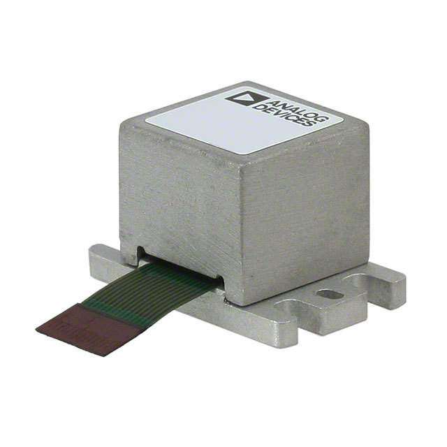
ADIS16227CMLZ产品简介:
ICGOO电子元器件商城为您提供ADIS16227CMLZ由Analog设计生产,在icgoo商城现货销售,并且可以通过原厂、代理商等渠道进行代购。 ADIS16227CMLZ价格参考。AnalogADIS16227CMLZ封装/规格:运动传感器 - 振动, Acceleration Sensor Digital Screw Mount Rectangular Connector - 14 Pos。您可以下载ADIS16227CMLZ参考资料、Datasheet数据手册功能说明书,资料中有ADIS16227CMLZ 详细功能的应用电路图电压和使用方法及教程。
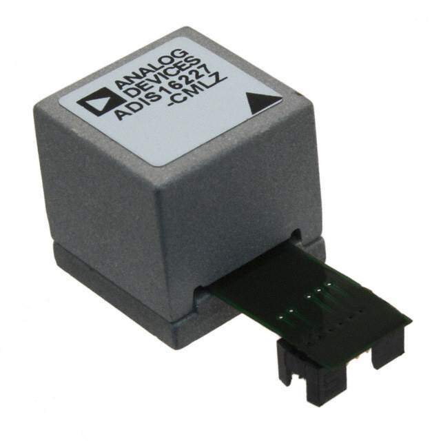
ADIS16227CMLZ是Analog Devices Inc.推出的一款高性能数字振动传感器,属于运动传感器中的振动检测类别。该器件集成了三轴数字加速度计和先进的时域/频域信号处理功能,适用于需要精确振动测量与分析的工业应用。

其主要应用场景包括:工业机械的状态监控与预测性维护,如电机、泵、风机和齿轮箱等旋转设备的故障诊断;通过检测异常振动模式,及时发现轴承磨损、不平衡、不对中等机械问题,从而减少意外停机,提高系统可靠性。此外,ADIS16227CMLZ也广泛应用于结构健康监测、重型工程机械振动分析以及航空航天设备的性能评估。

该传感器具备嵌入式FFT(快速傅里叶变换)功能,可直接输出频谱数据,便于进行频域分析,无需外部复杂处理,简化了系统设计。其紧凑的LGA封装和高抗冲击能力,使其适合在恶劣工业环境中长期稳定运行。因此,ADIS16227CMLZ特别适用于智能工厂、工业物联网(IIoT)和自动化系统中的高端振动监测解决方案。
| 参数 | 数值 |
| 产品目录 | |
| 描述 | SENSOR VIBRATION -70+70G MODUL加速计 Digital Tri-axial Vibration Sensor |
| 产品分类 | 震动传感器运动与定位传感器 |
| 品牌 | Analog Devices |
| 产品手册 | |
| 产品图片 |
|
| rohs | RoHS 合规性豁免无铅 / 符合限制有害物质指令(RoHS)规范要求 |
| 产品系列 | 加速计,Analog Devices ADIS16227CMLZiMEMS®, iSensor™ |
| 数据手册 | |
| 产品型号 | ADIS16227CMLZ |
| 产品种类 | 加速计 |
| 传感器类型 | 加速 |
| 传感轴 | Triple |
| 分辨率 | 16 bit |
| 功率-额定值 | 3.15 V ~ 3.6 V / 43mA |
| 加速 | 70 g |
| 商标 | Analog Devices |
| 安装类型 | 螺钉安装 |
| 安装风格 | SMD/SMT |
| 封装 | Bulk |
| 封装/外壳 | 14 模块,带连接器 |
| 封装/箱体 | Aluminum Package with Flex Connector |
| 工作温度 | -40°C ~ 125°C |
| 工厂包装数量 | 1 |
| 感应范围 | -70 ~ 70 g |
| 接口 | SPI |
| 数字输出-位数 | 16 bit |
| 数字输出-总线接口 | SPI |
| 最大工作温度 | + 125 C |
| 最小工作温度 | - 40 C |
| 标准包装 | 1 |
| 灵敏度 | 1.192 mg/LSB |
| 特性 | 可编程 |
| 电源电压-最大 | 3.6 V |
| 电源电压-最小 | 3.15 V |
| 电源电流 | 43 uA |
| 端接 | 矩形连接器 - 14 位置 |
| 系列 | ADIS16227 |
| 输出类型 | Digital |


- 商务部:美国ITC正式对集成电路等产品启动337调查
- 曝三星4nm工艺存在良率问题 高通将骁龙8 Gen1或转产台积电
- 太阳诱电将投资9.5亿元在常州建新厂生产MLCC 预计2023年完工
- 英特尔发布欧洲新工厂建设计划 深化IDM 2.0 战略
- 台积电先进制程称霸业界 有大客户加持明年业绩稳了
- 达到5530亿美元!SIA预计今年全球半导体销售额将创下新高
- 英特尔拟将自动驾驶子公司Mobileye上市 估值或超500亿美元
- 三星加码芯片和SET,合并消费电子和移动部门,撤换高东真等 CEO
- 三星电子宣布重大人事变动 还合并消费电子和移动部门
- 海关总署:前11个月进口集成电路产品价值2.52万亿元 增长14.8%
PDF Datasheet 数据手册内容提取
Digital Triaxial Vibration Sensor with FFT Analysis and Storage Data Sheet ADIS16227 FEATURES GENERAL DESCRIPTION Frequency domain triaxial vibration sensor The ADIS16227 iSensor® is a complete vibration sensing system Digital acceleration data, ± 70 g measurement range that combines wide bandwidth, triaxial acceleration sensing with Digital range settings: 1 g, 5 g, 20 g, 70 g advanced time domain and frequency domain signal processing. Sample rate: 100.2 kHz, 4 decimation filter settings Time domain signal processing includes a programmable decimation FFT, 512 point, real valued, all three axes (x, y, z) filter and selectable windowing funcEtion. Frequency domain Windowing options: rectangular, Hanning, flat top processing includes a 512 point, real-valued FFT for each axis, Programmable FFT averaging, up to 256 averages along with FFT averaging, which reduces the noise floor variation Storage, 16 FFT records on all three axes (x, y, z) for finer resolution. The 16-record FFT storage system offers T Programmable alarms, 6 spectral bands users the ability to track changes over time and to capture FFTs 2-level settings for warning and fault definition with multiple decimation filter settings. Adjustable response delay to reduce false alarms The 22 kHz seEnsor resonance and 100.2 kSPS sample rate Trigger modes: SPI command, timer, external trigger provide a frequency response that is suitable for machine-health Multirecord capture for selected filter settings applications. The aluminum core provides excellent mechanical Manual capture mode for time-domain data collection coupling to the MEMS acceleration sensors. An internal clock Internal self-test with status flags drLives the data sampling and signal processing system during all Digital temperature and power supply measurements operations, which eliminates the need for an external clock 2 auxiliary digital I/Os source. The data capture function has three modes that offer SPI-compatible serial interface O several options to meet the needs of many different applica- Serial number and device ID tions. Single-supply operation: 3.15 V to 3.6 V Operating temperature range: −40°C to +125°C The SPI and data buffer structure provide convenient access 15 mm × 15 mm × 15 mm aluminum package, flex connector to wide bandwidth sensor data. The ADIS16227 also offers a S digital temperature sensor and digital power supply measure- APPLICATIONS ments. Vibration analysis The ADIS16227 is available in a 15 mm × 15 mm × 15 mm module Condition monitoring B with a threaded hole for stud mounting with a 10-32 UNF screw. Machine health The dual-row, 1 mm, 14-pin, flexible connector enables simple Instrumentation, diagnostics user interface and installation. The ADIS16227 is footprint and Safety shutoff sensing pin-for-pin compatible with the ADIS16223. It has an extended O operating temperature range of −40°C to +125°C. FUNCTIONAL BLOCK DIAGRAM DIO1 DIO2 RST VDD ADIS16227 OINUPTUPTU/T ALARMS MANPAOGWEEMRENT GND CS TRMIAEMXISAL CONTROLLER RCEOGNISTTREORLS SENSOR SCLK SPI PORT TEMP DIN SENSOR ADC CBAUPFTFUERRE WFIINFLFDTTEORW SRTEOCROARGDE REOGUITSPTUETRS DOUT SUPPLY 09425-001 Figure 1. Rev. B Information furnished by Analog Devices is believed to be accurate and reliable. However, no responsibility is assumed by Analog Devices for its use, nor for any infringements of patents or other One Technology Way, P.O. Box 9106, Norwood, MA 02062-9106, U.S.A. rights of third parties that may result from its use. Specifications subject to change without notice. No license is granted by implication or otherwise under any patent or patent rights of Analog Devices. Tel: 781.329.4700 www.analog.com Trademarks and registered trademarks are the property of their respective owners. Fax: 781.461.3113 ©2010–2012 Analog Devices, Inc. All rights reserved.
ADIS16227 Data Sheet TABLE OF CONTENTS Features .............................................................................................. 1 Spectral Alarms ............................................................................... 13 Applications ....................................................................................... 1 Alarm Definition ........................................................................ 13 General Description ......................................................................... 1 Alarm Indicator Signals ............................................................. 14 Functional Block Diagram .............................................................. 1 Alarm Flags and Conditions ..................................................... 15 Revision History ............................................................................... 2 Alarm Status ................................................................................ 15 Specifications ..................................................................................... 3 Worst-Condition Monitoring ................................................... 15 Timing Specifications .................................................................. 4 Reading Output Data ................................E..................................... 16 Absolute Maximum Ratings ............................................................ 5 Reading Data from the Data Buffer ......................................... 16 ESD Caution .................................................................................. 5 Accessing FFT Record Data ...................................................... 16 T Pin Configuration and Function Descriptions ............................. 6 Data Format ................................................................................ 16 Theory of Operation ........................................................................ 7 Power Supply/Temperature ....................................................... 17 Sensing Element ........................................................................... 7 FFT Event HeadEer ...................................................................... 17 Signal Processing .......................................................................... 7 System Tools .................................................................................... 18 User Interface ................................................................................ 7 Global Commands ..................................................................... 18 Basic Operation ................................................................................. 8 StatuLs/Error Flags ....................................................................... 18 SPI Write Commands .................................................................. 8 Operation Managment .............................................................. 18 SPI Read Commands ................................................................... 8 Input/Output Functions ............................................................ 19 O Data Recording and Signal Processing ........................................ 10 Self-Test ....................................................................................... 19 Recording Modes ........................................................................ 10 Flash Memory Management ..................................................... 20 Recording Times ......................................................................... 10 Device Identification .................................................................. 20 S Power-Down ............................................................................... 11 Applications Information .............................................................. 21 Record Storage Mode ................................................................. 11 Mounting Guidelines ................................................................. 21 Sample Rate Options ......................................B............................ 11 Getting Started ............................................................................ 21 Windowing Options ................................................................... 11 Interface Board ........................................................................... 21 Range ............................................................................................ 12 Outline Dimensions ....................................................................... 22 Offset Correction ......................O.................................................. 12 Ordering Guide .......................................................................... 22 FFT Averaging ............................................................................ 12 FFT Record Flash Endurance ................................................... 12 REVISION HISTORY 5/12—Rev. A to Rev. B Changes to Alarm Trigger Settings Section, Enable Alarm Changes to Table 10 ........................................................................ 10 Settings Section, Table 27, Table 28, Table 30, and Table 31 ............................................................................................ 14 2/12—Rev. 0 to Rev. A Change to Alarm Indicator Section ............................................. 19 Changes to Dual Memory Structure Section ................................ 7 Change to Table 14 ......................................................................... 11 10/10—Revision 0: Initial Version Rev. B | Page 2 of 24
Data Sheet ADIS16227 SPECIFICATIONS T = −40°C to +125°C, VDD = 3.3 V, unless otherwise noted. A Table 1. Parameter Test Conditions/Comments Min Typ Max Unit ACCELEROMETERS Measurement Range T = 25°C ±70 g A Sensitivity, FFT T = 25°C, 0 g to 70 g range setting 1.192 mg/LSB A Sensitivity, Time Domain T = 25°C 2.384 mg/LSB A Sensitivity Error TA = 25°C E±5 % Nonlinearity With respect to full scale ±0.2 ±2 % Cross-Axis Sensitivity 2.6 % Alignment Error With respect to package 1.5 Degree T Offset Error T = 25°C −19.1 +19.1 g A Offset Temperature Coefficient 5 mg/°C Output Noise T = 25°C, 100.2 kHz sample rate option 467 mg rms A Output Noise Density T = 25°C, 10 Hz to 1 kHz E 3.3 mg/√Hz A Bandwidth X/Y-axes, ±5% flatness 7.75 kHz X/Y-axes, ±10% flatness 9.0 kHz Z-axis, ±5% flatness 13 kHz L Z-axis, ±10% flatness 14.25 kHz −3 dB from 10 Hz magnitude 26 kHz Sensor Resonant Frequency 22 kHz O LOGIC INPUTS1 Input High Voltage, V 2.0 V INH Input Low Voltage, V 0.8 V INL Logic 1 Input Current, I V = 3.3 V ±0.2 ±1 µA INH IH Logic 0 Input Current, I V S= 0 V INL IL All Except RST −40 −60 µA RST −1 mA Input Capacitance, CIN B 10 pF DIGITAL OUTPUTS1 Output High Voltage, V I = 1.6 mA 2.4 V OH SOURCE Output Low Voltage, V I = 1.6 mA 0.4 V OL SINK FLASH MEMORY O Endurance2 10,000 Cycles Data Retention3 T = 85°C, see Figure 18 20 Years J START-UP TIME4 Initial Startup 190 ms Reset Recovery5 RST pulse low or Register GLOB_CMD[7] = 1 54 ms Sleep Mode Recovery 2.5 ms CONVERSION RATE REC_CTRL[11:8] = 0x1 (SR0 sample rate selection) 100.2 kSPS Clock Accuracy 3 % POWER SUPPLY Operating voltage range, VDD 3.15 3.3 3.6 V Power Supply Current Record mode, T = 25°C 43 52 mA A Sleep mode, T = 25°C 230 µA A 1 The digital I/O signals are 5 V tolerant. 2 Endurance is qualified as per JEDEC Standard 22, Method A117, and measured at −40°C, +25°C, +85°C, and +125°C. 3 Retention lifetime equivalent at junction temperature (TJ) = 85°C as per JEDEC Standard 22, Method A117. Retention lifetime depends on junction temperature. 4 The start-up times presented reflect the time it takes for data collection to begin. 5 The RST pin must be held low for at least 15 ns. Rev. B | Page 3 of 24
ADIS16227 Data Sheet TIMING SPECIFICATIONS T = 25°C, VDD = 3.3 V, unless otherwise noted. A Table 2. Parameter Description Min1 Typ Max Unit f SCLK frequency 0.01 2.25 MHz SCLK t Stall period between data, between 16th and 17th SCLK 15.4 µs STALL t Chip select to SCLK edge 48.8 ns CS t DOUT valid after SCLK edge 100 ns DAV t DIN setup time before SCLK rising edge 24.4 ns DSU E t DIN hold time after SCLK rising edge 48.8 ns DHD t SCLK rise time 12.5 ns SR t SCLK fall time 12.5 ns SF tDF, tDR DOUT rise/fall times T5 12.5 ns t CS high after SCLK edge 5 ns SFS 1 Guaranteed by design, not tested. E Timing Diagrams L tSR CS tSF tCS O tSFS 1 2 3 4 5 6 15 16 SCLK tDAV DOUT MSB DB14 DB13 SDB12 DB11 DB10 DB2 DB1 LSB tDSU tDHD DIN R/W A6 B A5 A4 A3 A2 D2 D1 LSB 09425-002 Figure 2. SPI Timing and Sequence O tSTALL CS SCLK 09425-003 Figure 3. DIN Bit Sequence Rev. B | Page 4 of 24
Data Sheet ADIS16227 ABSOLUTE MAXIMUM RATINGS Table 3. Table 4. Package Characteristics Parameter Rating Package Type θ θ Device Weight JA JC Acceleration 14-Lead Module 31°C/W 11°C/W 6.5 grams Any Axis, Unpowered 2000 g Any Axis, Powered 2000 g ESD CAUTION VDD to GND −0.3 V to +6.0 V Digital Input Voltage to GND −0.3 V to +5.3 V Digital Output Voltage to GND −0.3 V to +3.6 V E Analog Inputs to GND −0.3 V to +3.6 V Operating Temperature Range −40°C to +125°C Storage Temperature Range −65°C to +150°C T Stresses above those listed under Absolute Maximum Ratings may cause permanent damage to the device. This is a stress rating only; functional operation of the device at these or any other conditions above those indicated in the operational E section of this specification is not implied. Exposure to absolute maximum rating conditions for extended periods may affect device reliability. L O S B O Rev. B | Page 5 of 24
ADIS16227 Data Sheet PIN CONFIGURATION AND FUNCTION DESCRIPTIONS aY aZ TOP VIEW LOOK THROUGH PINS ARE NOT VISIBLE FROM THIS VIEW E aX T 1412108 6 4 2 PIN 2 1311E9 7 5 3 1 PIN 13 PIN 1 1. THE ARROWS ASSOCIATED WITH aX, aY, AND aZ DEFINE THE DIRECTION OF 2 . MVOEAULTTOIPNCUGITT CYRO ECNGHNIASENTCGETREOS RT.H EAXTA PMRPOLDE:U SCAEMS TAE PCO PS/NIT CIVLEM O-1U0T7P-0U2T-L IMN- LADC-AC.ELERATION 09425-004 Figure 4. Pin Configuration Table 5. Pin Function Descriptions O Pin No. Mnemonic Type1 Description 1, 4, 9, 10 GND S Ground 2, 6 NC I No Connect 3 DIO2 S I/O Digital Input/Output Line 2 5 DIO1 I/O Digital Input/Output Line 1 7 RST I Reset, Active Low 8 VDD S Power Supply, 3.3 V B 11 DIN I SPI, Data Input 12 DOUT O2 SPI, Data Output 13 SCLK I SPI, Serial Clock 14 CS I SPI, Chip Select O 1 S is supply, O is output, I is input, and I/O is input/output. 2 DOUT is an output when CS is low. When CS is high, DOUT is in a three-state, high impedance mode. Rev. B | Page 6 of 24
Data Sheet ADIS16227 THEORY OF OPERATION The ADIS16227 is a triaxial, wide bandwidth, vibration-sensing CAPTURE system. It combines a triaxial MEMS accelerometer with a TRIAXIAL BUFFER MEMS OUTPUT sampling and advanced signal processing system. The SPI- SENSOR REGISTERS S L A cacooccmnetsprsoa lttsoib. flere pqouretn acnyd d uosmera irne gviisbterar tsitornu cdtautrae a pnrdo vmidaen yc ounsveern ient SETNEMSOPR ADC CONTROLLER CONTROL SPI PORT SPI SIGN REGISTERS SENSING ELEMENT Digital vibration sensing in the ADIS16227 starts with a wide CLOCK E 09425-006 bandwidth MEMS accelerometer core on each axis, which provides Figure 6. Simplified Sensor Signal Processing Diagram a linear motion-to-electrical transducer function. Figure 5 provides USER INTERFACE a basic physical diagram of the sensing element and its response to linear acceleration. It uses a fixed frame and a moving frame SPI Interface T to form a differential capacitance network that responds to linear The user registers manage user access to both sensor data and acceleration. Tiny springs tether the moving frame to the fixed configuration inputs. Each 16-bit register has its own unique bit frame and govern the relationship between acceleration and assignment anEd two addresses: one for its upper byte and one for physical displacement. A modulation signal on the moving plate its lower byte. Table 8 provides a memory map for each register, feeds through each capacitive path into the fixed frame plates and along with its function and lower byte address. The data into a demodulation circuit, which produces the electrical signal collection and configuration command uses the SPI, which L that is proportional to the acceleration acting on the device. consists of four wires. The chip select (CS) signal activates the ANCHOR SPI interface, and the serial clock (SCLK) synchronizes the serial data lines. Input commands clock into the DIN pin, one PLATE MOVABLE O bit at a time, on the SCLK rising edge. Output data clocks out of CAPACITORS FRAME the DOUT pin on the SCLK falling edge. When the SPI is used as a slave device, the DOUT contents reflect the information ON FPILXAETDES requested using a DIN command. RATI S Dual Memory Structure LE UNIT SENSING CE CELL The user registers provide addressing for all input/output operations C UNIT A MPOLVAINTGE FCOELRLCING in the SPI interface. The control registers use a dual memory B structure. The controller uses SRAM registers for normal operation, including user-configuration commands. The flash memory provides nonvolatile storage for control registers that O ANCHOR 09425-005 thhaev efl aflsahs hm beamckourpy r(esqeeu iTreasb ale m 8)a.n Sutaolr filnagsh c uopndfiagtue rcaotmiomn adnadta in Figure 5. MEMS Sensor Diagram (GLOB_CMD[6] = 1, DIN = 0xBE40). When the device powers SIGNAL PROCESSING on or resets, the flash memory contents load into the SRAM, and the device starts producing data according to the configuration Figure 6 offers a simplified block diagram for the ADIS16227. in the control registers. The signal processing stage includes time domain data capture, digital decimation/filtering, windowing, FFT analysis, FFT MANUAL FLASH averaging, and record storage. See Figure 13 for more details on BACKUP the signal processing operation. NONVOLATILE VOLATILE FLASH MEMORY SRAM (NO SPI ACCESS) SPI ACCESS START-UP RESET 09425-007 Figure 7. SRAM and Flash Memory Diagram Rev. B | Page 7 of 24
ADIS16227 Data Sheet BASIC OPERATION The ADIS16227 uses a SPI for communication, which enables Table 8 provides a list of user registers with their lower byte a simple connection with a compatible, embedded processor addresses. Each register consists of two bytes that each have their platform, as shown in Figure 8. The factory default configuration own, unique 7-bit addresses. Figure 9 relates each register’s bits for DIO1 provides a busy indicator signal that transitions low to their upper and lower addresses. when an event completes and data is available for user access. Uansde tDhIeO D2I, Oif_ nCeTceRsLsa rreyg. ister (see Table 59) to reconfigure DIO1 15 14 13UPP12ER B11YTE10 9 8 7 6 5LOW4ER B3YTE2 1 0 09425-009 Figure 9. Generic Register Bit Definitions VDD +3.3V SPI WRITE COMMANDS E 8 SPYRSOTCEEMSSOR SS 14 CS ADIS16227 User control registers govern many internal operations. The SPI MASTER SPI SLAVE DIN bit sequence in Figure 12 provides the ability to write to SCLK 13 SCLK these registers, one byte at a tTime. Some configuration changes MOSI 11 DIN and functions require only one write cycle. For example, set MISO 12 DOUT GLOB_CMD[11] = 1 (DIN = 0xBF08) to start a manual capture IRQ1 5 DIO1 sequence. The manual capture starts immediately after the last bit E IRQ2 3 DIO2 clocks into DIN (16th SCLK rising edge). Other configurations may 1 4 9 10 09425-008 reqCuSire writing to both bytes. Figure 8. Electrical Hook-Up Diagram L SCLK TPianb Nlea 6m. eG eneric Master FPurnoccteisosno r Pin Names and Functions DIN 09425-010 O Figure 10. SPI Sequence for Manual Capture Start (DIN = 0xBF08) SS Slave select IRQ1, IRQ2 Interrupt request inputs (optional) SPI READ COMMANDS MOSI Master output, slave input A single register read requires two 16-bit SPI cycles that also use MISO Master input, slave output the bit assignments in Figure 12. The first sequence sets R/W = 0 S SCLK Serial clock and communicates the target address (Bits[A6:A0]). Bits[D7:D0] The ADIS16227 SPI interface supports full duplex serial are don’t care bits for a read DIN sequence. DOUT clocks out the communication (simultaneous transmit and receive) and uses requested register contents during the second sequence. The the bit sequence shown in Figure 12. Table 7 pBrovides a list of second sequence can also use DIN to set up the next read. Figure 11 the most common settings that require attention to initialize a provides a signal diagram for all four SPI signals while reading processor serial port for the ADIS16227 SPI interface. the PROD_ID register (see Table 63) pattern. In this diagram, DIN = 0x5600 and DOUT reflect the decimal equivalent of 16,227. Table 7. Generic Master ProcessOor SPI Settings Processor Setting Description CS Master ADIS16227 operates as a slave. SCLK SCLK Rate ≤ 2.25 MHz Bit rate setting. SPI Mode 3 Clock polarity/phase DIN (CPOL = 1, CPHA = 1). M16S-BB-itF irst SBhiti fste rqeugeisntceer/. data length. DOUT DOUT = 0011 1111 0110 0011 = 0x3F63 = 16,227 = PROD_ID 09425-011 Figure 11. Example SPI Read, PROD_ID, Second Sequence CS SCLK DIN R/W A6 A5 A4 A3 A2 A1 A0 D7 D6 D5 D4 D3 D2 D1 D0 R/W A6 A5 DOUT DB15 DB14DB13DB12DB11DB10 DB9 DB8 DB7 DB6 DB5 DB4 DB3 DB2 DB1 DB0 DB15 DB14 DB13 N1.ODTOEUSTBITSAREBASED ONTHEPREVIOUS16-BITSEQUENCE(R/W=0). 09425-012 Figure 12. Example SPI Read Sequence Rev. B | Page 8 of 24
Data Sheet ADIS16227 Table 8. User Register Memory Map Register Flash Name Access Backup Address Default Function Reference FLASH_CNT Read only Yes 0x00 N/A Status, flash memory write count Table 61 X_NULL Read only Yes 0x02 0x0000 X-axis accelerometer offset correction Table 18 Y_NULL Read only Yes 0x04 0x0000 Y-axis accelerometer offset correction Table 18 Z_NULL Read only Yes 0x06 0x0000 Z-axis accelerometer offset correction Table 18 REC_FLSH_CNT N/A No 0x08 N/A Record flash write/erase counter Table 20 SUPPLY_OUT Read only Yes 0x0A 0x8000 Output, power supply during capture Table 48 TEMP_OUT Read only Yes 0x0C 0x8000 Output, temperature during capture Table 50 FFT_AVG Read/write Yes 0x0E 0x0008 Control, number of FFT records to aveErage Table 19 BUF_PNTR Read/write Yes 0x10 0x0000 Control, buffer address pointer Table 43 REC_PNTR Read/write Yes 0x12 0x0000 Control, record address pointer Table 44 X_BUF Read only No 0x14 0x8000 Output, buffer for x-axis acceleration data Table 45 T Y_BUF Read only No 0x16 0x8000 Output, buffer for y-axis acceleration data Table 45 Z_BUF Read only No 0x18 0x8000 Output, buffer for z-axis acceleration data Table 45 REC_CNTR Read/write No 0x1A 0x0000 Control, record counter Table 13 E REC_CTRL Read/write Yes 0x1C 0x1130 Control, record control register Table 10 REC_PRD Read/write Yes 0x1E 0x0000 Control, record period (automatic mode) Table 11 ALM_F_LOW Read/write N/A 0x20 0x0000 Alarm, spectral band lower frequency limit Table 24 ALM_F_HIGH Read/write N/A 0x22 0x0000 AlaLrm, spectral band upper frequency limit Table 25 ALM_X_MAG1 Read/write N/A 0x24 0x0000 Alarm, x-axis, Alarm 1 level Table 26 ALM_Y_MAG1 Read/write N/A 0x26 0x0000 Alarm, y-axis, Alarm 1 level Table 27 ALM_Z_MAG1 Read/write N/A 0x28 0x0000 Alarm, z-axis, Alarm 1 level Table 28 O ALM_X_MAG2 Read/write N/A 0x2A 0x0000 Alarm, x-axis, Alarm 2 level Table 29 ALM_Y_MAG2 Read/write N/A 0x2C 0x0000 Alarm, y-axis, Alarm 2 level Table 30 ALM_Z_MAG2 Read/write N/A 0x2E 0x0000 Alarm, z-axis, Alarm 2 level Table 31 ALM_PNTR Read/write Yes 0x30 0x0000 Alarm, spectral alarm band pointer Table 23 S ALM_S_MAG Read/write Yes 0x32 0x0000 Alarm, system alarm level Table 32 ALM_CTRL Read/write Yes 0x34 0x0080 Alarm, configuration Table 22 DIO_CTRL Read/write Yes 0x36 0x000F Control, functional I/O configuration Table 59 GPIO_CTRL Read/write Yes B0x38 0x0000 Control, general-purpose I/O Table 60 Reserved N/A N/A 0x3A N/A Reserved N/A DIAG_STAT Read only No 0x3C 0x0000 Status, system error flags Table 58 GLOB_CMD Write only No 0x3E N/A Control, global command register Table 57 ALM_X_STAT Read onlyO N/A 0x40 0x0000 Alarm, x-axis, status for spectral alarm bands Table 33 ALM_Y_STAT Read only N/A 0x42 0x0000 Alarm, y-axis, status for spectral alarm bands Table 34 ALM_Z_STAT Read only N/A 0x44 0x0000 Alarm, z-axis, status for spectral alarm bands Table 35 ALM_X_PEAK Read only N/A 0x46 0x0000 Alarm, x-axis, peak value (most severe alarm) Table 36 ALM_Y_PEAK Read only N/A 0x48 0x0000 Alarm, y-axis, peak value (most severe alarm) Table 37 ALM_Z_PEAK Read only N/A 0x4A 0x0000 Alarm, z-axis, peak value (most severe alarm) Table 38 TIME_STAMP_L Read only N/A 0x4C 0x0000 Record time stamp, lower word Table 54 TIME_STAMP_H Read only N/A 0x4E 0x0000 Record time stamp, upper word Table 55 Reserved N/A N/A 0x50 to 0x51 N/A Reserved N/A LOT_ID1 Read only Yes 0x52 N/A Lot identification code Table 62 LOT_ID2 Read only Yes 0x54 N/A Lot identification code Table 62 PROD_ID Read only Yes 0x56 0x3F63 Product identifier; convert to decimal = 16,227 Table 63 SERIAL_NUM Read only Yes 0x58 N/A Serial number Table 64 ALM_X_FREQ Read only N/A 0x70 0x0000 Alarm, x-axis, frequency of most severe alarm Table 39 ALM_Y_FREQ Read only N/A 0x72 0x0000 Alarm, y-axis, frequency of most severe alarm Table 40 ALM_Z_FREQ Read only N/A 0x74 0x0000 Alarm, z-axis, frequency of most severe alarm Table 41 REC_INFO Read only N/A 0x76 N/A Record settings Table 53 Rev. B | Page 9 of 24
ADIS16227 Data Sheet DATA RECORDING AND SIGNAL PROCESSING The ADIS16227 provides a number of registers for configuring For example, set DIO_CTRL[7:0] = 0x2F (DIN = 0xB62F) to its data collection and signal processing operation (see Table 9). configure DIO2 as a positive external trigger input and Figure 13 provides a signal flow diagram, which describes many maintain the DIO1 factory default configuration as a positive of these settings. busy indicator. In manual mode, the start command triggers a recording for an averaged FFT and stops after the recording is Table 9. Sampling/Signal Processing Register Summary complete. In automatic mode, the start command executes a Register Address Description recording, and a timer continues to trigger recordings based on X_NULL 0x02 X-axis offset correction the record period setting in REC_PRD (see Table 11). Y_NULL 0x04 Y-axis offset correction E Z_NULL 0x06 Z-axis offset correction Table 11. REC_PRD Register Bit Descriptions REC_FLSH_CNT 0x08 Record, flash write cycle counter Bits Description (Default = 0x0000) FFT_AVG 0x0E Record, FFT averages [15:10] Not used REC_CNTR 0x1A Record, counter [9:8] Scale for data bits T REC_CTRL 0x1C Record, data processing 00 = 1 second/LSB REC_PRD 0x1E Record, automatic mode period 01 = 1 minute/LSB GLOB_CMD 0x3E Trigger, record commands 10 = 1 hoEur/LSB [7:0] Data bits, binary format, range = 0 to 255 The record control register is REC_CTRL (see Table 10), which provides external controls for sample rates, dynamic range, RECORDING TIMES record storage, recording mode, and power management. L The automatic recording period (REC_PRD) must be greater Table 10. REC_CTRL Bit Descriptions than the total recording time. Use the following equations to Bits Description (Default = 0x1130) calculate the recording time: [15:14] Not used O Manual time mode [13:12] Window setting: T =T +T +T +T 00 = rectangular, 01 = Hanning, 10 = flat top, 11 = N/A R S PT ST AST [11] SR3, fs ÷ 512 (1 = enabled for analysis) FFT modes [10] SR2, fs ÷ 64 (1 = enabled for analysis) S T =N ×(T +T +T )+T +T [9] SR1, f ÷ 8 (1 = enabled for analysis) R F S PT FFT ST AST s [8] SR0, fs (1 = enabled for analysis) The storage time (TST) applies only when a storage method is [7] Power-down between each recording (1 = enabled) selected in REC_CTRL[3:2]. See Table 10 for more details on B [6] Not used the record storage setting. The alarm scan time (T ) applies AST [5:4] Signal range: only when the alarms are enabled in ALM_CTRL[4:0]. See 00 = 0 g to 1 g, 01 = 0 g to 5 g, 10 = 0 g to 20 g, 11 = 0 g Table 22 for more details on enabling the alarms. to 70 g [3:2] Storage method: O Table 12. Available Records 00 = none, 01 = alarm trigger, 10 = all, 11 = N/A Function Time (ms) [1:0] Recording mode: Sample Time, T See Table 15 S 00 = manual, 01 = automatic, 10 = manual time, 11 = N/A Processing Time, T 10.4 PT FFT Time, T 26.6 RECORDING MODES FFT Number of FFT Averages, N See Table 19 F REC_CTRL[1:0] provides three modes for triggering: (1) manual, Storage Time, T 120.0 ST (2) automatic, and (3) manual time domain. The manual and Alarm Scan Time, T 2.21 AST automatic modes produce FFT events, which include data collection, filtering, windowing, FFT analysis, and record storage (if selected). The manual time domain mode produces time-domain data in the buffer. All three modes require an external trigger, using either the SPI interface or one of the auxiliary digital I/O lines, DIO1 or DIO2. For the SPI external trigger option, set GLOB_CMD[11] = 1 (DIN = 0x3F08). For the digital I/O option, use the DIO_CTRL register (see Table 59) to configure either DIO1 or DIO2 as an external trigger input. Rev. B | Page 10 of 24
Data Sheet ADIS16227 Table 14. Sample Rate Settings and Filter Performance POWER-DOWN Sample Rate Bin Width Bandwidth Noise Set GLOB_CMD[1] = 1 (DIN = 0xBE02) to power down the Setting (SPS) (Hz) (Hz) (mg) ADIS16227. To reduce power consumption, set REC_CTRL[7] SR0 100,189 196 26,000 467 = 1 to automatically power down after a record has completed. SR1 12,524 25 6,262 260 Toggle the CS line from high to low to wake the device up and SR2 1566 3.1 783 100 place it in an idle state, where it waits for the next command. SR3 196 0.38 98 38 When configured as an external trigger option, toggling DIO1 Table 15 provides the data sampling time (T) for each sample or DIO2 can wake the device up as well. Using DIO1 or DIO2 S rate setting. This represents the time it takes to record data for for this purpose avoids the potential for multiple devices all three axes of vibration data. E contending for DOUT when waking up with the CS line approach. After completing the record cycle, the device remains Table 15. Sample Times, T S awake. Use GLOB_CMD[1] to put it back to sleep after reading Sample Rate Setting Sample Time (ms), T S the record data. SR0, REC_CTRL[8] = 1 T 5.27 RECORD STORAGE MODE SR1, REC_CTRL[9] = 1 42.15 SR2, REC_CTRL[10] = 1 337.17 After the ADIS16227 finishes processing FFT data, it stores the SR3, REC_CTRL[11] = 1 2697.39 data into the FFT buffer, where it is available for external access E using the SPI and x_BUF registers. REC_CTRL[3:2] provides If more than one sample rate setting is active in REC_CTRL[11:8], programmable conditions for writing buffer data into the FFT the sample rate setting automatically updates after each FFT records, which are in nonvolatile flash memory locations. Set event and waits for the next trigger input. The order of priority L REC_CTRL[3:2] = 01 to store FFT buffer data into the flash starts with the highest sample rate enabled and works toward the memory records only when an alarm condition is met. Set lowest after each REC_CTRL[11:8] write cycle. When used in REC_CTRL[3:2] = 10 to store every set of FFT data into the conjunction with automatic trigger mode and record storage, flash memory locations. The flash memory record provides O FFT analysis for each sample rate option requires no further space for a total of 16 records. Each record stored in flash user inputs, except for collecting the data. Depending on the memory contains a header and frequency domain (FFT) data number of FFT averages, the time period between each sample from all three axes (x, y, and z). When all 16 records are full, rate selection may be quite large. Note that selecting multiple new records do not load into the flash memory. TheS sample rates reduces the number of records available for each REC_CNTR register (see Table 13) provides a running count sample rate setting, as shown in Table 16. for the number of records that are stored. Set GLOB_CMD[8] = Table 16. Available Records 1 (DIN = 0xBF01) to clear all of the records in flash memory. B Number of Sample Rates Selected Available Records 1 16 Table 13. REC_CNTR Bit Descriptions 2 8 Bits Description (Default = 0x0000) 3 5 [15:5] Not used O 4 4 [4:0] Total number of records taken, range = 0 to 16, binary WINDOWING OPTIONS SAMPLE RATE OPTIONS REC_CTRL[13:12] provide three options for pre-FFT The analog-to-digital converter (ADC) samples each accelero- windowing of time data. For example, set REC_CTRL[13:12] = meter sensor at a rate of 100.2 kSPS (f). REC_CTRL[11:8] provide s 01 to use the Hanning window, which offers the best amplitude four different sample rate options for FFT analysis: SR0 (f), s resolution of the peaks between frequency bins and minimal SR1(f ÷ 8), SR2 (f ÷ 64), and SR3 (f ÷ 512). The reduced rates s s s broadening of peak amplitudes. The rectangular and flat top come from a decimation filter, which reduces the bandwidth windows are also available because they are common windowing and bin widths. See Figure 13 for the filter location in the signal options for vibration monitoring. The flat top window provides processing diagram and Table 14 for the performance trade-offs accurate amplitude resolution with a trade-off of broadening associated with each sample rate setting. the peak amplitudes. Rev. B | Page 11 of 24
ADIS16227 Data Sheet RANGE FFT AVERAGING REC_CTRL[5:4] provide four range options for scaling The FFT averaging function records a programmable number acceleration data prior to the FFT analysis stage. For example, of FFTs and combines them into a single, averaged FFT record. set REC_CTRL[5:4] = 10 to set the peak acceleration (A ) to This function is useful in reducing the variation of the FFT MAX 5 g. See Table 17 for the resolution associated with each setting noise floor, which enables detection of lower vibration levels. To and Figure 13 for the location of this operation in the signal enable this function, write the number of averages to FFT_AVG. flow diagram. Setting FFT_AVG = 0x0000 has the same effect as setting FFT_AVG = 0x0001: no averaging. Setting FFT_AVG ≥ 0x0100 Table 17. Range Setting and LSB Weights results in a setting of 256. Therefore, set FFT_AVG[15:8] = 0x01 Range Setting (g) Time Mode FFT Mode (DIN = 0x8F01) to establish the maximum average setting of (REC_CTRL[5:4]) (mg/LSB) (mg/LSB) E 256. Another example configuration is to set FFT_AVG = 0 to 1 0.0305 0.0153 0x00F0 (DIN = 0x8F00, DIN = 0x8EF0) to establish an average 0 to 5 0.1526 0.0763 setting of 240. 0 to 20 0.6104 0.3052 T 0 to 70 2.3842 1.1921 Table 19. FFT_AVG Register Bit Descriptions Bits Description (Default = 0x0008) OFFSET CORRECTION [15:9] Not used E The x_NULL registers (see Table 18) contain the offset [8:0] Number of FFT averages for a single record, correction factors generated when using the internal, autonull N in Figure 13, range = 1 to 256, binary F command. They represent the K factor in Figure 13 and follow O FFT RECORD FLASH ENDURANCE the digital format in Table 18. Set GLOB_CMD[0] =1 (DIN = L 0xBE01) and wait for 681 ms to execute this function. The REC_FLSH_CNT register (see Table 20) increments each time that all 16 records have FFT data. Table 18. X_NULL, Y_NULL, and Z_NULL Bit Descriptions Bits Description (Default = 0x0000) OTable 20. REC_FLSH_CNT Bit Descriptions [15:0] Offset correction factor, twos complement, Bits Description 2.3842 mg/LSB [15:0] Flash write cycle count, record data only, binary S RANGE-SCALE SETTING FFT RECORDS—NONVOLATILE FLASH MEMORY BKAsM=A XA M= APXE ÷A 2K1 5FROM REC_CTRL[5:4] REFCFOTRD REFCFOTRD REFCFOTRD REFCFOTRD OFFSET CORRECTION 0 1 m 15 KO = X_NULL, Y_NULL, Z_NULL SAMPLE RATE SETTING WINDOW SETTING REC_CTRL[11:8O] Ko Ks REC_CTRL[13:12] NNFF== #F FOTF_ AAVVGE[R8A:0G]ES mRE =C R_CETCR_LC[N3T:2R] TAMRCEIACMXESILS 100kSPS N1AKN =a 1xK ÷NA + WINDOW FFT AVE(FNRFFAT)GE BUFFFFTER R BAEUGNFDISF STEEPRRI 09425-016 Figure 13. Signal Flow Diagram, REC_CTRL[1:0] = 00 or 01, FFT Analysis Modes Rev. B | Page 12 of 24
Data Sheet ADIS16227 SPECTRAL ALARMS The alarm function offers six spectral bands for alarm ALARM DEFINITION detection. Each spectral band has high and low frequency The alarm function provides six programmable spectral bands, definitions, along with two different trigger thresholds (Alarm 1 as shown in Figure 14. Each spectral alarm band has lower and and Alarm 2) for each accelerometer axis. Table 21 provides a upper frequency definitions for all four sample rate options. It summary of each register used to configure the alarm function. also has two independent trigger level settings, which are useful Table 21. Alarm Function Register Summary for systems that value warning and fault condition indicators. Register Address Description ALM_F_HIGH ALM_F_LOW ALM_F_LOW 0x20 Alarm frequency, lower limit E ALM_F_HIGH 0x22 Alarm frequency, upper limit ALM_X_MAG1 0x24 X-Alarm Trigger Level 1 (warning) ALM_x_MAG2 ALM_x_MAG1 ALM_Y_MAG1 0x26 Y-Alarm Trigger Level 1 (warning) ALM_Z_MAG1 0x28 Z-Alarm Trigger Level 1 (warning) E T D ALM_X_MAG2 0x2A X-Alarm Trigger Level 2 (fault) TU NI ALM_Y_MAG2 0x2C Y-Alarm Trigger Level 2 (fault) G A M ALM_Z_MAG2 0x2E Z-Alarm Trigger Level 2 (fault) E ALM_PNTR 0x30 Alarm pointer ALM_S_MAG 0x32 System alarm trigger level ALM_CTRL 0x34 Alarm configuration DIAG_STAT 0x3C Alarm status L 1 2 3 4 5 6 AALLMM__XY__SSTTAATT 00xx4402 XY--aallaarrmm ssttaattuuss FREQUENCY 09425-020 Figure 14. Spectral Band Alarm Setting Example, ALM_PNTR = 0x03 ALM_Z_STAT 0x44 Z-alarm status O ALM_X_PEAK 0x46 X-alarm peak Select the spectral band for configuration by writing its number ALM_Y_PEAK 0x48 Y-alarm peak (1 to 6) to ALM_PNTR[2:0] (see Table 23). Then, select the ALM_Z_PEAK 0x4A Z-alarm peak sample rate setting using ALM_PNTR[9:8]. This number ALM_X_FREQ 0x70 X-axis alarm frequency oSf peak alarm represents a binary number, which corresponds to the x in the ALM_Y_FREQ 0x72 Y-axis alarm frequency of peak alarm SRx sample rates settings associated with REC_CTRL[11:8] (see ALM_Z_FREQ 0x74 Z-axis alarm frequency of peak alarm Table 10). For example set ALM_PNTR[7:0] = 0x05 (DIN = 0xB005) to select Alarm Spectral Band 5 and set The ALM_CTRL register (see Table 22) pBrovides control bits ALM_PNTR[15:8] = that enable each axis’ spectral alarms, configures the system 0x02 (DIN = 0xB102) to select the SR2 sample rate option alarm, sets the record delay for the spectral alarms, and from Table 14, 1,566 SPS. configures the clearing function for the DIAG_STAT error flags. O Table 23. ALM_PNTR Bit Assignments Table 22. ALM_CTRL Bit Descriptions Bits Description (Default = 0x0000) Bits Description (Default = 0x0080) [15:10] Not used [15:12] Not used [9:8] Sample rate setting, range: 0 to 3 [11:8] Response delay, range: 0 to 15; represents the number [7:3] Not used of spectral records for each spectral alarm before a [2:0] Spectral band number, range: 1 to 6 spectral alarm flag is set high [7] Latch DIAG_STAT error flags, which requires a clear status command (GLOB_CMD[4]) to reset the flags to 0 (1 = enabled, 0 = disabled) [6] Enable DIO1 as an Alarm 1 output indicator and enable DIO2 as an Alarm2 output indicator (1 = enabled) [5] System alarm comparison polarity 1 = trigger when less than ALM_MAGS[11:0] 0 = trigger when greater than ALM_MAGS[11:0] [4] System alarm, 1 = temperature 0 = power supply [3] Alarm S enable (ALM_S_MAG), 1 = enabled, 0 = disabled [2] Alarm Z enable (ALM_Z_MAG), 1 = enabled, 0 = disabled [1] Alarm Y enable (ALM_Y_MAG), 1 = enabled, 0 = disabled [0] Alarm X enable (ALM_X_MAG), 1 = enabled, 0 = disabled Rev. B | Page 13 of 24
ADIS16227 Data Sheet Alarm Band Frequency Definitions Table 28. ALM_Z_MAG1 Bit Assignments After the spectral band and sample rate settings are set, Bits Description (Default = 0x0000) program the lower and upper frequency boundaries by writing [15:0] Z-axis Alarm Trigger Level 1, 16-bit unsigned; see their bin numbers to the ALM_F_LOW (see Table 24) and REC_CTRL[5:4] and Table 17 for the scale factor ALM_F_HIGH (see Table 25) registers. Use the bin width definitions in Table 14 to convert a frequency into a bin number Table 29. ALM_X_MAG2 Bit Assignments for this definition. Calculate the bin number by dividing the Bits Description (Default = 0x0000) frequency by the bin width associated with the sample rate [15:0] X-axis Alarm Trigger Level 2, 16-bit unsigned; see REC_CTRL[5:4] and Table 17 for the scale factor setting. For example, 3400 Hz, divided by 196 Hz/bin (SR0 setting), rounded to the nearest integer, is equal to 17, or 0x12. E Table 30. ALM_Y_MAG2 Bit Assignments Therefore, set ALM_F_LOW[7:0] = 0x11 (DIN = 0xA011) to Bits Description (Default = 0x0000) establish 3400 Hz as the lower frequency for the SR0 sample [15:0] Y-axis Alarm Trigger Level 2, 16-bit unsigned; see rate setting. REC_CTRL[5:4] and Table 17 for the scale factor T Table 24. ALM_F_LOW Bit Assignments Table 31. ALM_Z_MAG2 Bit Assignments Bits Description (Default = 0x0000) Bits Description (Default = 0x0000) [15:8] Not used [15:0] Z-axis AlaErm Trigger Level 1, 16-bit unsigned; see [7:0] Lower frequency, bin number, range = 0 to 255 REC_CTRL[5:4] and Table 17 for the scale factor Table 25. ALM_F_HIGH Bit Assignments Table 32. ALM_S_MAG Bit Assignments Bits Description (Default = 0x0000) Bits LDescription (Default = 0x0000) [15:8] Not used [15:0] System alarm trigger level, data format matches target [7:0] Upper frequency, bin number, range = 0 to 255 from ALM_CTRL[4] Alarm Trigger Settings OEnable Alarm Settings The ALM_x_MAG1 and ALM_x_MAG2 registers provide two Before configuring the spectral alarm registers, clear their independent trigger settings for all three axes of acceleration current contents by setting GLOB_CMD[9] = 1 (DIN = 0xBF02). data. They use the data format established by the range setting After completing the spectral alarm band definitions, enable the in REC_CTRL[5:4] and recording mode in REC_CTRL[1S:0]. settings by setting GLOB_CMD[12] = 1 (DIN = 0xBF10). The For example, when using the 0 g to 1 g mode for FFT analysis, device ignores the save command if any of these locations have 3277 LSB is equivalent to 500.07 mg. To set the critical alarm to already been written to. 500.07 mg when using the 0 g to 1 g range option in REC_CTRL2 B ALARM INDICATOR SIGNALS for FFT records, set ALM_X_MAG2 = 0x0CCD (DIN = 0xAD0C, 0xACCD). See Table 10 and Table 17 for more information on DIO_CTRL[5:2] and ALM_CTRL[6] provide controls for formatting each trigger level. Note that trigger settings associated establishing DIO1 and DIO2 as dedicated alarm output indicator with Alarm 2 should be greater thOan the trigger settings for signals. Use DIO_CTRL[5:2] to select Alarm function for DIO1 Alarm 1. In other words, the alarm magnitude settings should and/or DIO2; then set ALM_CTRL[6] = 1 to enable DIO1 to meet the following criteria: serve as an Alarm 1 indicator and DIO2 as an Alarm 2 indicator. ALM_X_MAG2 > ALM_X_MAG1 This setting establishes DIO1 to indicate Alarm 1 (warning) ALM_Y_MAG2 > ALM_Y_MAG1 conditions and DIO2 to indicate Alarm 2 (critical) conditions. ALM_Z_MAG2 > ALM_Z_MAG1 Table 26. ALM_X_MAG1 Bit Assignments Bits Description (Default = 0x0000) [15:0] X-axis Alarm Trigger Level 1, 16-bit unsigned; see REC_CTRL[5:4] and Table 17 for the scale factor Table 27. ALM_Y_MAG1 Bit Assignments Bits Description (Default = 0x0000) [15:0] Y-axis Alarm Trigger Level 1, 16-bit unsigned; see REC_CTRL[5:4] and Table 17 for the scale factor Rev. B | Page 14 of 24
Data Sheet ADIS16227 ALARM FLAGS AND CONDITIONS Table 35. ALM_Z_STAT Bit Assignments Bits Description (Default = 0x0000) The FFT header (see Table 52) contains both generic alarm flags [15] Alarm 2 on Band 6, 1 = alarm set, 0 = no alarm (DIAG_STAT[13:8] (see Table 58) and spectral band-specific [14] Alarm 1 on Band 6, 1 = alarm set, 0 = no alarm alarm flags (ALM_x_STAT, see Table 33, Table 34 and Table 35). [13] Alarm 2 on Band 5, 1 = alarm set, 0 = no alarm The FFT header also contains magnitude (ALM_x_PEAK, see [12] Alarm 1 on Band 5, 1 = alarm set, 0 = no alarm Table 36, Table 37 and Table 38) and frequency information [11] Alarm 2 on Band 4, 1 = alarm set, 0 = no alarm (ALM_x_FREQ, see Table 39, Table 40, and Table 41) associated [10] Alarm 1 on Band 4, 1 = alarm set, 0 = no alarm with the highest magnitude of vibration content in the record. [9] Alarm 2 on Band 3, 1 = alarm set, 0 = no alarm ALARM STATUS [8] Alarm 1 on Band 3, 1 = alarm set, 0 = no alarm E [7] Alarm 2 on Band 2, 1 = alarm set, 0 = no alarm The ALM_x_STAT registers, in Table 33, Table 34, and Table 35, [6] Alarm 1 on Band 2, 1 = alarm set, 0 = no alarm provide alarm bits for each spectral band on the current sample [5] Alarm 2 on Band 1, 1 = alarm set, 0 = no alarm rate option. [4] Alarm 1 on BanTd 1, 1 = alarm set, 0 = no alarm Table 33. ALM_X_STAT Bit Assignments [3] Not used Bits Description (Default = 0x0000) [2:0] Most critical alarm condition, spectral band, range: 1 to 6 [15] Alarm 2 on Band 6, 1 = alarm set, 0 = no alarm WORST-COENDITION MONITORING [14] Alarm 1 on Band 6, 1 = alarm set, 0 = no alarm [13] Alarm 2 on Band 5, 1 = alarm set, 0 = no alarm The ALM_x_PEAK registers (see Table 36, Table 37, and Table [12] Alarm 1 on Band 5, 1 = alarm set, 0 = no alarm 38) contain the peak magnitude for the worst-case alarm [11] Alarm 2 on Band 4, 1 = alarm set, 0 = no alarm coLndition in each axis. The ALM_x_FREQ registers (see Table [10] Alarm 1 on Band 4, 1 = alarm set, 0 = no alarm 39, Table 40, and Table 41) contain the frequency bin number [9] Alarm 2 on Band 3, 1 = alarm set, 0 = no alarm for the worst-case alarm condition. [8] Alarm 1 on Band 3, 1 = alarm set, 0 = no alarm O Table 36. ALM_X_PEAK Bit Assignments [7] Alarm 2 on Band 2, 1 = alarm set, 0 = no alarm Bits Description (Default = 0x0000) [6] Alarm 1 on Band 2, 1 = alarm set, 0 = no alarm [15:0] Alarm peak, x-axis, accelerometer data format [5] Alarm 2 on Band 1, 1 = alarm set, 0 = no alarm [4] Alarm 1 on Band 1, 1 = alarm set, 0 = no alarm S Table 37. ALM_Y_PEAK Bit Assignments [3] Not used Bits Description (Default = 0x0000) [2:0] Most critical alarm condition, spectral band, range: 1 to 6 [15:0] Alarm peak, y-axis, accelerometer data format Table 34. ALM_Y_STAT Bit AssignmeBnts Table 38. ALM_Z_PEAK Bit Assignments Bits Description (Default = 0x0000) Bits Description (Default = 0x0000) [15] Alarm 2 on Band 6, 1 = alarm set, 0 = no alarm [15:0] Alarm peak, z-axis, accelerometer data format [14] Alarm 1 on Band 6, 1 = alarm set, 0 = no alarm [13] Alarm 2 on Band 5,O 1 = alarm set, 0 = no alarm Table 39. ALM_X_FREQ Bit Assignments [12] Alarm 1 on Band 5, 1 = alarm set, 0 = no alarm Bits Description (Default = 0x0000) [11] Alarm 2 on Band 4, 1 = alarm set, 0 = no alarm [15:8] Not used [10] Alarm 1 on Band 4, 1 = alarm set, 0 = no alarm [7:0] Alarm frequency for x-axis peak alarm level, [9] Alarm 2 on Band 3, 1 = alarm set, 0 = no alarm FFT bin number, range: 0 to 255 [8] Alarm 1 on Band 3, 1 = alarm set, 0 = no alarm [7] Alarm 2 on Band 2, 1 = alarm set, 0 = no alarm Table 40. ALM_Y_FREQ Bit Assignments [6] Alarm 1 on Band 2, 1 = alarm set, 0 = no alarm Bits Description (Default = 0x0000) [5] Alarm 2 on Band 1, 1 = alarm set, 0 = no alarm [15:8] Not used [4] Alarm 1 on Band 1, 1 = alarm set, 0 = no alarm [7:0] Alarm frequency for y-axis peak alarm level, FFT bin number, range: 0 to 255 [3] Not used [2:0] Most critical alarm condition, spectral band, range: 1 to 6 Table 41. ALM_Z_FREQ Bit Assignments Bits Description (Default = 0x0000) [15:8] Not used [7:0] Alarm frequency for z-axis peak alarm level, FFT bin number, range: 0 to 255 Rev. B | Page 15 of 24
ADIS16227 Data Sheet READING OUTPUT DATA The ADIS16227 samples, processes, and stores x, y, and z accel- Table 43. BUF_PNTR Bit Descriptions eration data into the FFT buffer and FFT records (if selected). Bits Description (Default = 0x0000) In manual time mode, each axis’ record contains 512 samples [15:9] Not used for each axis. Otherwise, each record contains the 256-point [8:0] Data bits FFT result for each accelerometer axis. Table 42 provides a ACCESSING FFT RECORD DATA summary of registers that provide access to processed sensor data. The FFT records provide flash memory storage for FFT data. The REC_PNTR register (see Table 44) and record retrieve Table 42. Output Data Registers command in GLOB_CMD[13] (see TablEe 57) provide access to Register Address Description the FFT records, as shown in Figure 16. For example, set SUPPLY_OUT 0x0A Internal power supply REC_PNTR[7:0] = 0x0A (DIN = 0x920A) and GLOB_CMD[13] TEMP_OUT 0x0C Internal temperature = 1 (DIN = 0xBF20) to load FFT Record 10 in the FFT buffer BUF_PNTR 0x10 Data buffer index pointer T for SPI/register access. REC_PNTR 0x12 FFT record index pointer X_BUF 0x14 X-axis accelerometer buffer Table 44. REC_PNTR Bit Descriptions Y_BUF 0x16 Y- axis accelerometer buffer Bits DesEcription (Default = 0x0000) Z_BUF 0x18 Z- axis accelerometer buffer [15:4] Not used GLOB_CMD 0x3E FFT record retrieve command [3:0] Data bits TIME_STAMP_L 0x4C Time stamp, lower word FFT FFT FFT FFT TIME_STAMP_H 0x4E Time stamp, upper word LRECORD RECORD RECORD RECORD 0 1 m 15 REC_INFO 0x76 FFT record header information X Y Z X Y Z X Y Z X Y Z READING DATA FROM THE DATA BUFFER O m = REC_PNTR GLOB_CMD[13] = 1 After completing an FFT event and updating the data buffer, the ADIS16227 loads the first data samples from the data buffer SPI X Y Z REGISTERS ipnotion ttehre (xB_UBFU_FP rNeTgiRst)e tros (0sxe0e0 T0a0b. lTe h4e5 i)n adnedx speotisn tthere dbeuteffremSr iinnedse x BUFFFFTER 09425-019 which data samples load into the x_BUF registers. For example, Figure 16. FFT Record Access writing 0x009F to the BUF_PNTR register (DIN = 0x9100, DIN DATA FORMAT = 0x909F) causes the 160th sample in each data buffer location Table 45 provides the bit assignments for the x_BUF registers. to load into the x_BUF registers. The index poBinter increments The acceleration data format depends on the range scale and with every x_BUF read command, which causes the next set recording mode settings in REC_CTRL. See Table 10 for of capture data to load into each capture buffer register auto- configuration details and Table 17 for the scale factors matically. This enables a process-efficient method for reading all O associated with each setting. Table 46 provides some data 256 samples in a record, using sequential reads commands, formatting examples for FFT mode, and Table 47 offers some without having to manipulate BUF_PNTR. data formatting examples for the16-bit twos complement DATA IN BUFFERS LOAD INTO USER OUTPUT REGISTERS format used in manual time mode. X_BUF Table 45. X_BUF, Y_BUF, Z_BUF Bit Descriptions Bits Description (Default = 0x8000) 0 Y_BUF [15:0] Acceleration buffer registers Z_BUF BUF_PNTR Table 46. FFT Mode, 0 g to 5 g Range, Data Format Examples ACCELXE-ARXOIMSETER ACCELYE-ARXOIMSETER ACCELZE-ARXOIMSETER Acceleration (mg) LSB Hex Binary FFT FFT FFT BUFFER BUFFER BUFFER 4999.9237 65,535 0xFFFF 1111 1111 1111 1111 7.63 100 0x0064 0000 0000 0110 0100 256/512 0.1526 2 0x0002 0000 0000 0000 0010 FFT ANALYSIS 0.0763 1 0x0001 0000 0000 0000 0001 0 0 0x0000 0000 0000 0000 0000 SUPPLY_OUT ISNTTOERRENSA LD ASTAAM IPNL FINFGT BSYUSFTFEEMRS S.AMPLES, PROCESSES, AND TEMP_OUT 09425-013 Figure 15. Data Buffer Structure and Operation Rev. B | Page 16 of 24
Data Sheet ADIS16227 FFT EVENT HEADER Table 47. Acceleration Format, Time Domain, 0 g to 70 g Range Each FFT record has an FFT header, which contains Acceleration (mg) LSB Hex Binary information that fills all of the registers listed in Table 52. The +70,000 +29,360 0x72B0 0111 0010 1011 0000 information in these registers contains recording time, record +1001.358 +420 0x01A4 0000 0001 1010 0100 configuration settings, status/error flags, and several alarm +4.7684 +2 0x0002 0000 0000 0000 0010 outputs. The registers listed in Table 52 update with every +2.3842 +1 0x0001 0000 0000 0000 0001 record event and also update with record-specific information 0 0 0x0000 0000 0000 0000 0000 when using GLOB_CMD[13] to retrieve a data set from the −2.3842 −1 0xFFFF 1111 1111 1111 1111 FFT record. −4.7684 −2 0xFFFE 1111 1111 1111 1110 −1001.358 −420 0xFE5C 1111 1110 0101 1100 E Table 52. FFT Header Register Information −70,000 −29,360 0x8D50 1000 1101 0101 0000 Register Address Description POWER SUPPLY/TEMPERATURE DIAG_STAT 0x3C Alarm status ALM_X_STAT 0x40 TX-alarm status During every acceleration recording process, the ADIS16227 also ALM_Y_STAT 0x42 Y-alarm status measures power supply and internal temperature. It takes a ALM_Z_STAT 0x44 Z-alarm status 5.12 ms record of power supply measurements at a sample rate ALM_X_PEAK 0x46 X-alarm peak of 50 kHz and takes 64 samples of internal temperature data over E ALM_Y_PEAK 0x48 Y-alarm peak a period of 1.7 ms. The average of the power supply and internal ALM_Z_PEAK 0x4A Z-alarm peak temperature loads into the SUPPLY_OUT and TEMP_OUT TIME_STAMP_L 0x4C Time stamp, lower word registers, respectively. TIMLE_STAMP_H 0x4E Time stamp, upper word Table 48. SUPPLY_OUT Bits Descriptions ALM_X_FREQ 0x70 X-alarm frequency of peak alarm Bits Description (Default = 0x8000) ALM_Y_FREQ 0x72 Y-alarm frequency of peak alarm [15:12] Not used O ALM_Z_FREQ 0x74 Z-alarm frequency of peak alarm [11:0] Power supply, binary, +3.3 V = 0xA8F, 1.22 mV/LSB REC_INFO 0x76 FFT record header information The REC_INFO register (see Table 53) captures the settings Table 49. Power Supply Data Format Examples associated with the current FFT record. Supply Level (V) LSB Hex Binary S 3.6 2949 0xB85 1011 1000 0101 Table 53. REC_INFO Bit Descriptions 3.3 + 0.0012207 2704 0xA90 1010 1001 0000 Bits Description (Default = 0x0000) 3.3 2703 0xA8F 1010 1000 1111 [15:14] Sample rate setting: 3.3 − 0.0012207 2702 0xA8E B1010 1000 1110 00 = SR0, 01 = SR1, 10 = SR2, 11 = SR3 3.15 2580 0xA14 1010 0001 0100 [13:12] Window setting: 00 = rectangular, 01 = Hanning, 10 = flat top, 11 = N/A Table 50. TEMP_OUT Bit Descriptions [11:10] Signal range: Bits Description (DefaOult = 0x8000) 00 = 0 g to 1 g, 01 = 0 g to 5 g, 10 = 0 g to 20 g, 11 = [15:12] Not used 0 g to 70 g [11:0] Temperature data, offset binary, [9] Not used 1278 LSB = +25°C, −0.47°C/LSB [8:0] FFT averages, range: 1 to 256 Table 51. Internal Temperature Data Format Examples The TIME_STAMP_x registers (see Table 54 and Table 55) Temperature (°C) LSB Hex Binary provide a relative time stamp, which identifies the time for the 125 1065 0x429 0100 0010 1001 current FFT record. 25 + 0.47 1277 0x4FD 0100 1111 1101 Table 54. TIME_STMP_L Bit Descriptions 25 1278 0x4FE 0100 1111 1110 Bits Description (Default = 0x0000) 25 − 0.047 1279 0x4FF 0100 1111 1111 [15:0] Time stamp, low integer, binary, seconds 0 1331 0x533 0101 0011 0011 −40 1416 0x588 0101 1000 1000 Table 55. TIME_STMP_H Bit Descriptions Bits Description (Default = 0x0000) [15:0] Time stamp, high integer, binary, seconds Rev. B | Page 17 of 24
ADIS16227 Data Sheet SYSTEM TOOLS Table 56 provides an overview of the control registers that STATUS/ERROR FLAGS provide support for system level functions. The DIAG_STAT register (see Table 58) provides a number of status/error flags that reflect the conditions observed in a Table 56. System Tool Register Addresses recording during SPI communication and diagnostic tests. A Register Name Address Description 1 indicates an error condition, and all of the error flags are FLASH_CNT 0x00 Flash write cycle count sticky, which means that they remain until they are reset by DIO_CTRL 0x36 Digital I/O configuration setting GLOB_CMD[4] = 1 (DIN = 0xBE10) or by starting a GPIO_CTRL 0x38 General-purpose I/O control new recording event. DIAG_STAT[14:8] indicates which DIAG_STAT 0x3C Status, error flags E ALM_x_MAGx thresholds were exceeded during a recording GLOB_CMD 0x3E Global commands event. The flag in DIAG_STAT[3] indicates that the total LOT_ID1 0x52 Lot Identification Code 1 number of SCLK clocks is not a multiple of 16. LOT_ID2 0x54 Lot Identification Code 2 PROD_ID 0x56 Product identification Table 58. DIAG_STAT Bit DTescriptions SERIAL_NUM 0x58 Serial number Bits Description (Default = 0x0000) [15] Not used GLOBAL COMMANDS [14] System alarEm flag The GLOB_CMD register provides an array of single-write [13] Z-axis, Spectral Alarm 2 flag commands for convenience. Setting the assigned bit (see Table [12] Y-axis, Spectral Alarm 2 flag 57) to 1 activates each function. When the function completes, [11] X-axis, Spectral Alarm 2 flag the bit restores itself to 0. For example, clear the capture buffers by [10] LZ-axis, Spectral Alarm 1 flag setting GLOB_CMD[8] = 1 (DIN = 0xBF01). All of the commands [9] Y-axis, Spectral Alarm 1 flag in the GLOB_CMD register require the power supply be within [8] X-axis, Spectral Alarm 1 flag normal limits for the execution times listed in Table 57. O[7] Data ready/busy indicator (0 = busy, 1 = data ready) [6] Flash test result, checksum flag Table 57. GLOB_CMD Bit Descriptions [5] Self-test diagnostic error flag Bits Description Execution Time [4] Recording escape flag, indicates use of the SPI-driven [15] Clear x_NULL registers 35 µs interruption command, 0xE8 S [3] SPI communication failure, (SCLKs ≠ even multiple of 16) [14] Retrieve spectral alarm band infor- 40 µs mation from the ALM_PNTR setting [2] Flash update failure [13] Restore record data from flash 1.9 ms [1] Power supply above 3.625 V memory [0] Power supply below 3.125 V B [12] Save spectral alarm band registers 461 µs OPERATION MANAGMENT to flash memory [11] Record start/stop N/A The ADIS16227 SPI port supports two different communi- [10] Set BUF_PNTR = 0x0000 36 µs cation commands while it is processing data or executing a O [9] Clear spectral alarm band 25.8 ms command associated with the GLOB_CMD register: reading registers from flash DIAG_STAT (DIN = 0x3C00) and the escape code (DIN = [8] Clear records 25.9 ms 0xE8E8). The SPI ignores all other commands when the [7] Software reset 53.3 ms processor is busy. [6] Save registers to flash memory 29.3 ms Software Busy Indicator [5] Flash test, compare sum of flash 5.6 ms memory with factory value Use the DIAG_STAT read command to poll DIAG_STAT[7], [4] Clear DIAG_STAT register 36 µs which is equal to 0 when the processor is busy and equal to [3] Restore factory register settings 80.9 ms 1 when the processor is idle and data is ready for SPI commu- and clear the capture buffers nications. [2] Self-test, result in DIAG_STAT[5] 32.9 ms [1] Power-down N/A [0] Autonull 681 ms Rev. B | Page 18 of 24
Data Sheet ADIS16227 Software Escape Code Table 59. DIO_CTRL Bit Descriptions Bits Description (Default = 0x000F) The only SPI command available when the processor is busy [15:6] Not used is the escape code, which is 0xE8E8. Send this command in a [5:4] DIO2 function selection repeating pattern, with a small delay between each write cycle, 00 = general-purpose I/O (use GPIO_CTRL) to the DIN pin, while monitoring DIAG_STAT[7]. The follow- 01 = alarm indicator output (per ALM_CTRL) ing code example illustrates this process: 10 = trigger input DIAG_STAT = 0; 11 = busy indicator output DIAG_STAT = read_reg(0x3C); [3:2] DIO1 function selection while ((DIAG_STAT & 0x0080) == 0) 00 = general-purpose I/O (use GPIO_CTRL) { 01 = alarm indicator output (per ALM_CTRL) write_reg(0xE8E8) E 10 = trigger input delay_us(50) DIAG_STAT = read_reg(0x3C) 11 = busy indicator output } [1] DIO2 line polarity INPUT/OUTPUT FUNCTIONS 1 = active high T 0 = active low The DIO_CTRL register (see Table 59) provides configuration [0] DIO1 line polarity control options for the two digital I/O lines, DIO1 and DIO2. 1 = active high E Busy Indicator 0 = active low The busy indicator is an output signal that indicates internal General-Purpose I/O processor activity. This signal is active during data recording events If DIO_CTRL configures either DIO1 or DIO2 as a general- or internal processing (GLOB_CMD functions, for example). The L purpose digital line, use the GPIO_CTRL register in Table 60 to factory default setting for DIO_CTRL sets DIO1 as a positive, configure its input/output direction, set the output level when active high, busy indicator signal. When configured in this configured as an output, and monitor the status of an input. manner, use this signal to alert the master processor to read O data from data buffers. Table 60. GPIO_CTRL Bit Descriptions Trigger Input Bits Description (Default = 0x0000) [15:10] Not used The trigger function provides an input pin for starting record events with a signal pulse. Set DIO_CTRL[7:0] = 0x2SF (DIN = [9] DIO2 output level 1 = high 0xB62F) to configure DIO2 as a positive trigger input and keep 0 = low DIO1 as a busy indicator. To start a trigger, the trigger input signal [8] DIO1 output level must transition from low to high and then from high to low. The B 1 = high recording process starts on the high-to-low transition, as shown 0 = low in Figure 17, and the pulse duration must be at least 2.6 µs. [7:2] Reserved DIO2 Δt ≥ 2.6µs Δt [1] DIO2 direction control O DIO1 1 = output CAPTURE TIME 09425-014 [0] 0D I=O i1n pduiret ction control Figure 17. Manual Trigger/Busy Indicator Sequence Example 1 = output Alarm Indicator 0 = input DIO_CTRL[5:2] provide controls for establishing DIO1 and/or SELF-TEST DIO2 as a general alarm output indicator, which goes active when any of the flags in DIAG_STAT[13:8] are active. For example, set Set GLOB_CMD[2] = 1 (DIN = 0xBE02) to run an automatic DIO_CTRL[7:0] = 0x12 (DIN = 0xB612) to configure DIO2 as self-test routine, which reports a pass/fail result to DIAG_STAT[5]. a generic alarm indicator with an active high polarity. ALM_CTRL[6] (see Table 22) provides an additional control, which enables DIO2 to reflect Alarm 2 and DIO1 to reflect Alarm 1 when they are selected as alarm indicators in DIO_CTRL[5:2]. For example, set DIO_CTRL[7:0] = 0x17 (DIN = 0xB617) and set ALM_CTRL[6] = 1 (DIN = 0xB440) to establish DIO2 as an active- high Alarm 2 indicator and DIO1 as an active-high Alarm 1 indicator. Set GLOB_CMD[4] = 1 (DIN = 0xBE10) to clear the DIAG_STAT error flags and restore the alarm indicator signal to its inactive state. Rev. B | Page 19 of 24
ADIS16227 Data Sheet FLASH MEMORY MANAGEMENT DEVICE IDENTIFICATION Set GLOB_CMD[5] = 1 (DIN = 0xBE20) to run an internal Table 62. LOT_ID1 and LOT_ID2 Bit Descriptions checksum test on the flash memory, which reports a pass/fail Bits Description result to DIAG_STAT[6]. The FLASH_CNT register (see Table 61) [15:0] Lot identification code provides a running count of flash memory write cycles. This is a tool for managing the endurance of the flash memory. Figure 18 Table 63. PROD_ID Bit Descriptions quantifies the relationship between data retention and junction Bits Description temperature. [15:0] 0x3F63 = 16,227 Table 61. FLASH_CNT Bit Descriptions Table 64. SERIAL_NUM Bit Descriptions E Bits Description Bits Description [15:0] Binary counter for writing to flash memory [15:0] Serial number, lot specific T 600 s) E ar450 e Y N ( O TI EN300 L T E R 150 O 0 30 40 55JUNCT7IO0NTEM85PERAT1U00RE(°C12)5 135 150 09425-015 Figure 18. Flash/EE Memory Data Retention S B O Rev. B | Page 20 of 24
Data Sheet ADIS16227 APPLICATIONS INFORMATION MOUNTING GUIDELINES DIO1 and DIO2 signals. The connector is a dual row, 2 mm (pitch) connector that works with a number of ribbon cable The ADIS16227 provides a threaded hole for a 10-32 UNF systems, including 3M Part Number 152212-0100-GB (ribbon- machine screw. This hole is 9 mm deep, and the tapped depth crimp connector) and 3M Part Number 3625/12 (ribbon cable). is 7 mm. Use a torque of 15 inch-pounds when tightening the The LEDs (D1 and D2) provide visual indication of the DIO1 10-32 mounting fastener and make sure that the fastener doesn’t and DIO2 signals. bottom-out in the ADIS16227 when tightening. GETTING STARTED E When the power supply voltage of the ADIS16227 reaches 3.15 V, it executes a start-up sequence that places the device in manual FFT mode. The following code example initiates a manual data recording by setting GLOB_CMD[11] = 1 (DIN = 0xBF08) and T reads all 256 samples in the x-axis acceleration buffer, using DIN = 0x1400. The data from the first spi_reg_read is not valid because this command starts the process. The second spi_reg_read cthoem fmirsatn vda (ltihde d fairtsat. rTehadis i cnosiddee stehqeu eemnbceed pdreodd fuocre lso CopS), SpCroLdKu, caensd E 09425-017 Figure 19. Electrical Schematic DIN signals similar to the ones shown in Figure 11. L spi_write(BF08h); delay 30ms; Data(0) = spi_reg_read(14h); O For n = 0 to 255 Data(n) = spi_reg_read(14h); n = n + 1; S end INTERFACE BOARD The ADIS16227/PCBZ provides the ADIS16227 on a small printed circuit board (PCB) that simplifies Bthe connection to an existing processor system. A single 10-32 machine screw (Fastener Express, FHS1106-4I2) secures the ADIS16227CMLZ to the interface board. The first set of mounting holes on the interface b40o amrdasc hisi nine tshcere fwous.r T choren seercso onfOd t hseet P oCf mB oanudn tpinrogv hidoeless c pleraorvaindcees afo r 4- 09425-018 Figure 20. PCB Assembly View and Dimensions pattern that matches the ADISUSBZ evaluation system, using M2 × 0.4 mm machine screws. These boards are made of IS410 material and are 0.063 inches thick. The J1 connector uses Pin 1 through Pin 12 in this pattern. Pin 13 and Pin 14 are for future expansion, but they also provide convenient probe points for the Rev. B | Page 21 of 24
ADIS16227 Data Sheet OUTLINE DIMENSIONS 15.20 15.00SQ 14.80 E BOTTOMVIEW T 6.00 BCS Ø4.04 9 1.00BSC 10-32UNF 7 PITCH E Ø6.10 90°, 17.50NOM NEARSIDE L 0.50BCS TOPVIEW DETAILA 3.88NOM O 0.45NOM FRONTVIEW SIDEVIEW DETAILA S 15.20 15.00 14.80 4.20 4.10 B 4.00 9.20 0.54 NOM 98..0800 O 06-21-2010-A Figure 21. 14-Lead Module with Connector Interface (ML-14-2) Dimensions shown in millimeters ORDERING GUIDE Model1 Temperature Range Package Description Package Option ADIS16227CMLZ −40°C to +125°C 14-Lead Module with Connector Interface ML-14-2 ADIS16227/PCBZ Evaluation Board 1 Z = RoHS Compliant Part. Rev. B | Page 22 of 24
Data Sheet ADIS16227 NOTES E T E L O S B O Rev. B | Page 23 of 24
ADIS16227 Data Sheet NOTES E T E L O S B O ©2010–2012 Analog Devices, Inc. All rights reserved. Trademarks and registered trademarks are the property of their respective owners. D09425-0-5/12(B) Rev. B | Page 24 of 24