ICGOO在线商城 > 分立半导体产品 > 二极管 - 整流器 - 单 > UPS340E3/TR13

 Datasheet下载
- 型号: UPS340E3/TR13
- 制造商: American Microsemiconductor, Inc.
- 库位|库存: xxxx|xxxx
- 要求:
| 数量阶梯 | 香港交货 | 国内含税 |
| +xxxx | $xxxx | ¥xxxx |
查看当月历史价格
查看今年历史价格
UPS340E3/TR13产品简介:
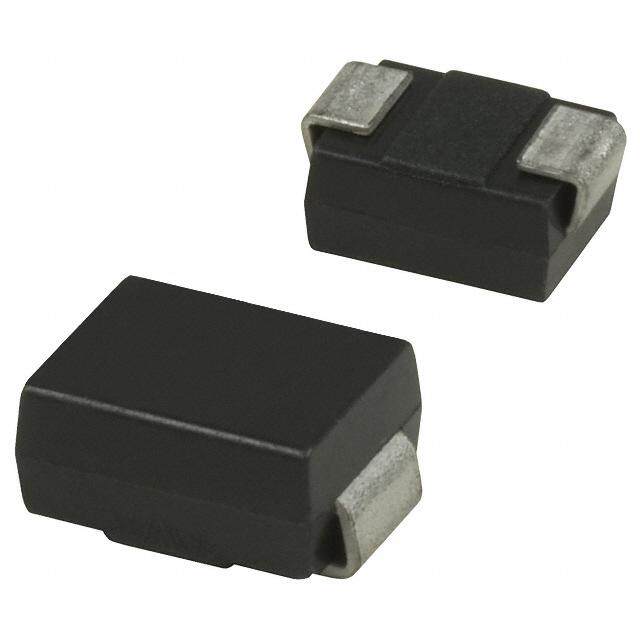
ICGOO电子元器件商城为您提供UPS340E3/TR13由American Microsemiconductor, Inc.设计生产,在icgoo商城现货销售,并且可以通过原厂、代理商等渠道进行代购。 UPS340E3/TR13价格参考。American Microsemiconductor, Inc.UPS340E3/TR13封装/规格:二极管 - 整流器 - 单, 肖特基 表面贴装 二极管 40V 3A Powermite 3。您可以下载UPS340E3/TR13参考资料、Datasheet数据手册功能说明书,资料中有UPS340E3/TR13 详细功能的应用电路图电压和使用方法及教程。
Microsemi Corporation(现为Microchip子公司)的UPS340E3/TR13是一款单整流二极管,属于通用型高效整流器件,广泛应用于各类电子设备中,主要功能是将交流电转换为直流电。

该型号二极管的典型应用场景包括:

1. 电源适配器与充电器:用于笔记本电脑、手机、平板等消费类电子产品的电源转换部分,实现AC/DC整流功能。

2. 开关电源(SMPS):在各类工业设备、服务器、通信设备的电源模块中,作为输入整流元件,具有高效率和良好热稳定性。

3. 逆变器与UPS系统:用于不间断电源(UPS)和逆变器中,协助在不同电源状态间切换并稳定输出。

4. 电机驱动与控制系统:在电机控制电路中用于整流和反向电压保护,确保系统稳定运行。

5. 家电设备:如微波炉、洗衣机、空调等家用电器的电源整流部分,提供可靠的电流转换支持。

UPS340E3/TR13采用表面贴装封装(SMA),适合自动化生产,具备较高的反向耐压(400V)和额定整流电流能力(1A),适用于中低功率应用场合。其优良的稳定性和耐用性使其在多种工业与消费类电子设备中得到广泛应用。
| 参数 | 数值 |
| 产品目录 | |
| 描述 | DIODE SCHOTTKY 40V 3A POWERMITE3 |
| 产品分类 | 单二极管/整流器 |
| 品牌 | Microsemi Commercial Components Group |
| 数据手册 | |
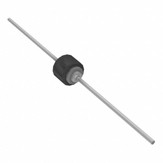
| 产品图片 |
|
| 产品型号 | UPS340E3/TR13 |
| rohs | 无铅 / 符合限制有害物质指令(RoHS)规范要求 |
| 产品系列 | - |
| 不同If时的电压-正向(Vf) | 500mV @ 3A |
| 不同 Vr、F时的电容 | 180pF @ 4V,1MHz |
| 不同 Vr时的电流-反向漏电流 | 500µA @ 40V |
| 二极管类型 | |
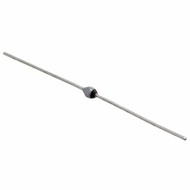
| 产品目录绘图 |
|
| 产品目录页面 | |
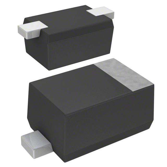
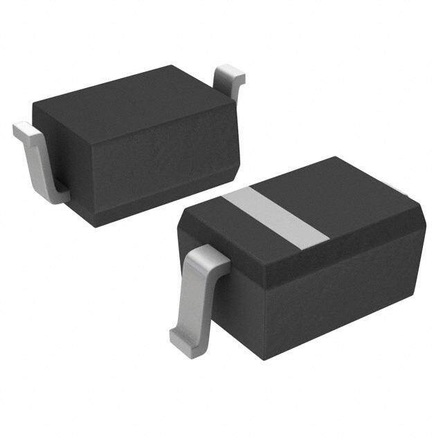
| 供应商器件封装 | Powermite 3 |
| 其它名称 | UPS340E3CT |
| 包装 | 剪切带 (CT) |
| 反向恢复时间(trr) | - |
| 安装类型 | 表面贴装 |
| 封装/外壳 | Powermite®3 |
| 工作温度-结 | -55°C ~ 125°C |
| 标准包装 | 1 |
| 热阻 | 3.2°C/W Jc |
| 电压-DC反向(Vr)(最大值) | 40V |
| 电流-平均整流(Io) | 3A |
| 速度 | 快速恢复 =< 500 ns,> 200mA(Io) |


- 商务部:美国ITC正式对集成电路等产品启动337调查
- 曝三星4nm工艺存在良率问题 高通将骁龙8 Gen1或转产台积电
- 太阳诱电将投资9.5亿元在常州建新厂生产MLCC 预计2023年完工
- 英特尔发布欧洲新工厂建设计划 深化IDM 2.0 战略
- 台积电先进制程称霸业界 有大客户加持明年业绩稳了
- 达到5530亿美元!SIA预计今年全球半导体销售额将创下新高
- 英特尔拟将自动驾驶子公司Mobileye上市 估值或超500亿美元
- 三星加码芯片和SET,合并消费电子和移动部门,撤换高东真等 CEO
- 三星电子宣布重大人事变动 还合并消费电子和移动部门
- 海关总署:前11个月进口集成电路产品价值2.52万亿元 增长14.8%


PDF Datasheet 数据手册内容提取
UPS340 3 A LOW Vf Schottky Barrier Rectifier DESCRIPTION KEY FEATURES In Microsemi(cid:146)s new Powermite3fi SMT In addition to its size advantages, ! High power surface mount W W package, these high efficiency ultrafast Powermite3fi package features include a full package. W rectifiers offer the power handing metallic bottom that eliminates the ! Guard Ring die construction for . transient protection. M capabilities previously found only in possibility of solder flux entrapment during much larger packages. They are ideal assembly, and a unique locking tab acts as ! Silicon Schottky rectifiers no ic reverse voltage recovery. r for SMD applications that operate at an integral heat sink. Its innovative design o ! Internal heat sink locking tabs s high frequencies. makes this device ideal for use with ! Low forward voltage. e m automatic insertion equipment. ! Full metallic bottom eliminates flux entrapment i .C IMPORTANT: For the most current data, consult MICROSEMI(cid:146)s website: http://www.microsemi.com ! Compatible with automatic O insertion equipment M ABSOLUTE MAXIMUM RATINGS AT 25º C ! Low profile-maximum height of 1mm supplied in 16 mm tape (UNLESS OTHERWISE SPECIFIED) reel- 5000 units/ 13” reel. Rating Symbol Value Unit Peak Repetitive Reverse Voltage VRRM Working Peak Reverse Voltage V 40 V RWM DC Blocking Voltage V APPLICATIONS/BENEFITS R RMS Reverse Voltage V 28 V ! Switching and Regulating Power R (RMS) Supplies. Average Rectified Output Current I 3 A o ! Charge Pump Circuits. Non-Repetitive Peak Forward Surge Current ! Reduces reverse recovery loss 8.3ms Single half sine wave Superimposed IFSM 50 A due to low IRM. on Rated Load @ T =100 ºC c ! Small foot print Storage Temperature T stg -55 to +150 ºC 190 X 300 mils Operating Temperature T op -55 to +125 ºC 1:1 Actual size THERMAL CHARACTERISTICS (UNLESS OTHERWISE SPECIFIED) Thermal Resistance Junction-to Bottom Rja (1) 2.5 ºC/Watt (1) When Mounted on PC board with 2 ounce copper pattern. UU PP SS 33 44 00 Copyright 2003 Microsemi Page 1 Rev. 0., 2003-02-12
UPS340 3 A LOW Vf Schottky Barrier Rectifier ELECTRICAL PARAMETERS @ 25°C (unless otherwise specified) Parameter Symbol Conditions Min Typ. Max Units W W W Forward Voltage (Note 1) I = 3 A , T =25 ºC 0.46 0.50 F j . I = 3 A , T =125 ºC 0.40 0.44 M V F j V Fm IF = 6 A , Tj =25 ºC 0.57 0.61 ic IF = 6 A , Tj =125 ºC 0.54 0.58 ro Reverse Break Down Voltage s e (Note 1) VBR IR = 0.5 mA 40 V m Reverse Current (Note1) VR = 40V, Tj = 25 ºC 15 500 uA i .C I V = 40V, T =100 ºC 10 20 mA O rm R j M Capacitance C V = 4 V; F = 1 MH 180 pF T R Z Note: 1 Short duration test pulse used to minimize self (cid:150) heating effect. EE LL EE CC TT RR II CC AA LL SS Copyright 2003 Microsemi Page 2 Rev. 0., 2003-02-12
UPS340 3 A LOW Vf Schottky Barrier Rectifier W W W . M ic r o s e m i . C O M Notes: 1. TA = TSOLDERING POINT, RΘJS = 3.4” C/W RΘsa = 0” C/W. 2. Device mounted on GETEK substrate, 2" x 2", 2 oz. copper , double-sided , cathode pad dimensions .075" x 1.0", anode pad dimensions 0.25" x 1.0". R in range of ΘJA 20-40(cid:176) C/W. 3. Device mounted on FRA-4 substrate, 2" x 2", 2 oz. copper, single-sided, pad layout R in range of 95 - 115(cid:176) C/W. ΘJA Copyright 2003 Microsemi Page 3 Rev. 0., 2003-02-12
UPS340 3 A LOW Vf Schottky Barrier Rectifier 16 mm TAPE W W W . M ic r o s e m i . C O M 13 INCH REEL PRODUCT PRELIMINARY DATA (cid:150) Information contained in this document is pre-production data, and is proprietary to Microsemi Corp. It may not be modified in any way without the express written consent of Microsemi Corp. Product referred to herein is not guaranteed to achieve preliminary or production status and product specifications, configurations, and availability may change at any time. Copyright 2003 Microsemi Page 4 Rev. 0., 2003-02-12
UPS340 3 A LOW Vf Schottky Barrier Rectifier W W W . M ic r o s e m i . C O M MM EE CC HH AA NN II CC AA LL Copyright 2003 Microsemi Page 5 Rev. 0., 2003-02-12
UPS340 3 A LOW Vf Schottky Barrier Rectifier NOTES: W W W . M ic r o s e m i . C O M NN OO TT EE SS Copyright 2003 Microsemi Page 6 Rev. 0., 2003-02-12
Mouser Electronics Authorized Distributor Click to View Pricing, Inventory, Delivery & Lifecycle Information: M icrosemi: UPS340e3/TR13