ICGOO在线商城 > 射频/IF 和 RFID > RF 放大器 > UPC2771TB-E3-A

 Datasheet下载
- 型号: UPC2771TB-E3-A
- 制造商: CEL
- 库位|库存: xxxx|xxxx
- 要求:
| 数量阶梯 | 香港交货 | 国内含税 |
| +xxxx | $xxxx | ¥xxxx |
查看当月历史价格
查看今年历史价格
UPC2771TB-E3-A产品简介:
ICGOO电子元器件商城为您提供UPC2771TB-E3-A由CEL设计生产,在icgoo商城现货销售,并且可以通过原厂、代理商等渠道进行代购。 UPC2771TB-E3-A价格参考¥询价-¥询价。CELUPC2771TB-E3-A封装/规格:RF 放大器, 射频放大器 IC 手机,GPS,PCS 900MHz ~ 1.5GHz SOT-363。您可以下载UPC2771TB-E3-A参考资料、Datasheet数据手册功能说明书,资料中有UPC2771TB-E3-A 详细功能的应用电路图电压和使用方法及教程。
CEL品牌的UPC2771TB-E3-A是一款RF(射频)放大器,属于射频前端模块中的关键元件。该器件主要应用于无线通信系统中,用于增强射频信号的强度,以确保信号在传输过程中的稳定性和可靠性。

其典型应用场景包括:

1. 无线基站设备:用于蜂窝通信系统(如4G LTE、5G)中的射频前端,提升基站接收和发射信号的能力。

2. 通信中继设备:在微波通信、卫星通信等中继系统中,作为信号放大单元,增强远距离传输的信号质量。

3. 工业通信系统:应用于工业自动化、远程监控等场景中的无线数据传输设备,提升通信距离和稳定性。

4. 测试测量仪器:用于射频信号分析仪、频谱仪等相关测试设备中,作为信号放大模块,提高测试精度。

5. 物联网(IoT)设备:在需要远距离无线通信的IoT设备中,如智能电表、远程传感器等,用于增强射频信号覆盖能力。

该器件具有低噪声、高增益和良好的线性性能,适用于高频段(如UHF、微波频段)应用,适合对信号质量和系统稳定性有较高要求的场景。
| 参数 | 数值 |
| 产品目录 | |
| 描述 | MMIC AMP 2.4GHZ SOT 363 |
| 产品分类 | |
| 品牌 | CEL |
| 数据手册 | |
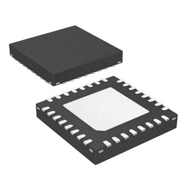
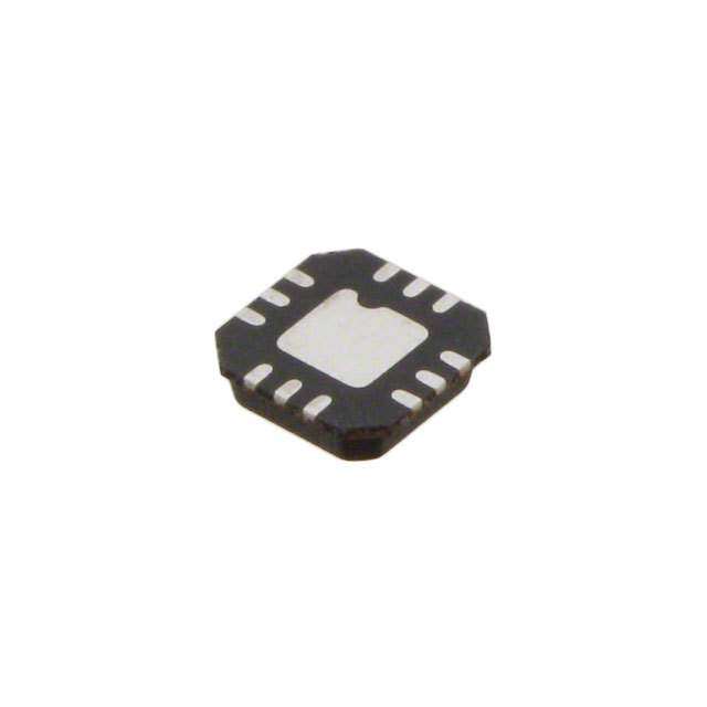
| 产品图片 |
|
| P1dB | 7dBm(5mW)~ 9.5dBm(8.9mW) |
| 产品型号 | UPC2771TB-E3-A |
| RF类型 | 手机,GPS,PCS |
| rohs | 无铅 / 符合限制有害物质指令(RoHS)规范要求 |
| 产品系列 | - |
| 产品目录页面 | |
| 供应商器件封装 | SOT-363 |
| 其它名称 | UPC2771TB-ADKR |
| 包装 | Digi-Reel® |
| 噪声系数 | 6dB ~ 7.5dB |
| 增益 | 18dB ~ 24dB |
| 封装/外壳 | 6-TSSOP,SC-88,SOT-363 |
| 标准包装 | 1 |
| 测试频率 | 1.5GHz |
| 电压-电源 | 2.7 V ~ 3.3 V |
| 电流-电源 | 36mA ~ 45mA |
| 频率 | 900MHz ~ 1.5GHz |


- 商务部:美国ITC正式对集成电路等产品启动337调查
- 曝三星4nm工艺存在良率问题 高通将骁龙8 Gen1或转产台积电
- 太阳诱电将投资9.5亿元在常州建新厂生产MLCC 预计2023年完工
- 英特尔发布欧洲新工厂建设计划 深化IDM 2.0 战略
- 台积电先进制程称霸业界 有大客户加持明年业绩稳了
- 达到5530亿美元!SIA预计今年全球半导体销售额将创下新高
- 英特尔拟将自动驾驶子公司Mobileye上市 估值或超500亿美元
- 三星加码芯片和SET,合并消费电子和移动部门,撤换高东真等 CEO
- 三星电子宣布重大人事变动 还合并消费电子和移动部门
- 海关总署:前11个月进口集成电路产品价值2.52万亿元 增长14.8%


PDF Datasheet 数据手册内容提取
BIPOLAR ANALOG INTEGRATED CIRCUIT UPC2771TB T 3 V, SUPER MINIMOLD MEDIUM POWER SI MMIC AMPLIFIER U FEATURES GAIN vs. FREQUENCY AND TEMPERATURE • HIGH GAIN: 21 dB at 900 to 1500 MHz Typical 24 • HIGH OUTPUT POWER: PSAT = +12.5 dBm at 900 MHz TA = -40˚ C +11 dBm at 1500 MHz 22 • LOW BIAS VOLTAGE: 3.0 V Typical, 2.7 V Minimum • SUPER SMALL PACKAGE: SOT-363 B) O d 20 +85˚ C • TAPE AND REEL PACKAGING OPTION AVAILABLE (S TA = +25˚ C TA = +85˚ C G n, DESCRIPTION ai 18 G The UPC2771TB is a Silicon Monolithic integrated circuit +25˚ C which is manufactured using the NESAT™ III process. The -16 -40˚ C NESAT III process produces transistors with fT approaching 20 VCC = 3.0 V GHz. The UPC2771TB is pin compatible and has comparable 14 performance as the larger UPC2771T, so it is suitable for use E 0.1 0.3 1.0 3.0 as a replacement to help reduce system size. The IC is housed Frequency, f (GHz) in a 6 pin super minimold or SOT-363 package. Operating on a 3 volt supply, this IC is ideally suited for hand-held, portable designs. NEC's stringent quality assurance and test procedures ensure S the highest reliability and performance. ELECTRICAL CHARACTERISTICS (TA = 25(cid:176) C, ZL = ZS = 50 W , VCC = 3.0 V) PART NUMBER UPC2771TB PACAKAGE OUTLINE S06 SYMBOLS PARAMETERS AND CONDITIONS UNITS MIN TYP MAX ICC Circuit Current (no signal) mA 36 45 GS Small Signal Gain, f = 900 MHz dB 19 21 24 f = 1500 MHz dB 18 21 24 fU Upper Limit Operating Frequency (The gain at fU is 3 dB down from the gain at 100 MHz) GHz 1.8 2.2 H P1dB 1 dB Compressed Output Power, f = 900 MHz dBm +9 +11.5 f = 1500 MHz dBm +7 +9.5 PSAT Saturated Output Power, f = 900 MHz dBm +12.5 f = 1500 MHz dBm +11 NF Noise Figure, f = 900 MHz dB 6 7.5 f = 1500 MHz dB 6 7.5 P RLIN Input Return Loss, f = 900 MHz dB 10 14 f = 1500 MHz dB 10 14 RLOUT Output Return Loss, f = 900 MHz dB 6.5 9.0 f = 1500 MHz dB 5.5 8.5 ISOL Isolation, f = 900 MHz dB 25 30 f = 1500 MHz dB 25 30 OIP3 SSB OutputThird Order Intercept Point f = 900, 902 MHz, POUT = +4 dBm dBm +13 f = 1500, 1502 MHz, POUT = +4 dBm dBm +10 PADJ1 Adjacent Channel Power 1, f = 900 mHz, p /4 QPSK wave1, POUT = +7 dBm D f = – 50 kHz dBc -61 D f = – 100 kHz dBc -72 PADJ2 Adjacent Channel Power 2, f = 1.5 GHz, p /4 QPSK wave1, POUT = +7 dBm D f = – 50 kHz dBc -59 D f = – 100 kHz dBc -71 Note: 1.p /4 QPSK modulated wave input, data rate 42 kbps, Filter roll off a = 0.5
UPC2771TB ABSOLUTE MAXIMUM RATINGS1 (TA = 25(cid:176) C) TEST CIRCUIT SYMBOLS PARAMETERS UNITS RATINGS VCC VCC Supply Voltage V 3.6 1000 pF ICC Total Supply Current mA 77.7 PIN Input Power dBm +13 T PT Total Power Dissipation2 mW 270 L=1000 nH TOP Operating Temperature (cid:176) C -40 to +85 6 TSTG Storage Temperature (cid:176) C -55 to +150 50 W 1 4 50 W IN OUT Notes: 1000 pF U1000 pF 1. Operation in excess of any one of these parameters may result in permanent damage. 2. Mounted on a 50 X 50 X 1.6 mm epoxy glass PWB (TA = 85(cid:176) C). 2, 3, 5 RECOMMENDED OPERATING CONDITIONS O SYMBOLS PARAMETERS UNITS MIN TYP MAX VCC Supply Voltage V 2.7 3 3.3 TOP Operating Temperature (cid:176)C -40 +25 +85 - TYPICAL PERFORMANCE CURVES (TA = 25(cid:176) C) E CIRCUIT CURRENT vs. VOLTAGE CIRCUIT CURRENT vs. TEMPERATURE 50 50 A) 40 S A) 40 m m nt, I (CC 30 nt, I (CC 30 e e Curr 20 Curr20 uit A uit Circ 10 Circ10 0 0 0 1 2 3 4 -60 -40 -20 0 20 40 60 80 100 Supply VoHltage, VCC (V) Temperature ((cid:176) C) GAIN AND NOISE FIGURE INPUT RETURN LOSS AND vs. FREQUENCY AND VOLTAGE OUTPUT RETURN LOSS vs. FREQUENCY 24 P 0 VCC = 2.7V VCC = 3.0V VCC = 3.3V VCC = 3.0V 22 20 GS -10 RLout VCC = 3.3V VCC = 3.0 V 18 B) B) d Gain, G (dS 111642 VCC = 3.3 V VCC = 3.0V VCC = 2.7 V 7 e, NF (dB) Return Loss (-20 RLin ur -30 10 5 g Fi NF e 8 VCC = 2.7 V s oi 6 3 N -40 0.1 0.3 1.0 3.0 0.1 0.3 1.0 3.0 Frequency, f (GHz) Frequency, f (GHz)
UPC2771TB TYPICAL PERFORMANCE CURVES (TA = 25(cid:176) ) OUTPUT POWER vs. ISOLATION vs. FREQUENCY INPUT POWER AND VOLTAGE 0 15 VCC = 3.0V VCC = 3.3 V f = 900 MHz T -10 m) 10 B) dB L (d-20 (UT VCC = 2.7 V ation, ISO-30 Power, PO 5 UVCC = 3.0 V Isol put 0 -40 ut O O -50 -5 0.1 0.3 1.0 3.0 -25 -20 -15 -10 -5 0 Frequency, f (GHz) Input Power, PIN (dBm) SATURATED OUTPUT POWER vs. -SATURATED OUTPUT POWER vs. FREQUENCY AND VOLTAGE FREQUENCY AND TEMPERATURE m) 17 Em) 17 B Pin = -3 dBm B Pin = -3 dBm d d (T), 15 VCC = 3.3 V (T), 15 SA SA TA = +85˚C PO( 13 PO( 13 er, er, TA = +25˚C w VCC = 3.0 V S w ut Po 11 VCC = 2.7 V ut Po 11 TA = -40˚C p p ut 9 ut 9 O O d d e e at 7 at 7 ur A ur at at S 5 S 5 0.1 0.3 1.0 3.0 0.1 0.3 1.0 3.0 Frequency, f (GHz) Frequency, f (GHz) H P
UPC2771TB OUTLINE DIMENSIONS (Units in mm) LEAD CONNECTIONS UPC2771TB PACKAGE OUTLINE S06 (Top View) (Bottom View) 2.1– 0.1 T 1.25– 0.1 3 4 4 3 H 2.0– 0.2 0 . 2 +0.1(cid:13) 2 -0 2 5 5 2 0.65 3 4 C U 1.3 0.65 2 5 1 6 6 1 1 6 DOT ON(cid:13) 1. INPUT O BACK SIDE 2. GND 0.9 – 0.1 3. GND 4. OUTPUT 0.7 5. GND 6. VCC +0.1(cid:13) 0(cid:17)~0.1 0.15 -0.5 - E PIN DESCRIPTION Pin Pin Applied Description Internal No. Name Voltage Equivalent (V) S Circuit 1 Input — Signal input pin. An internal matching circuit, configured 6 with resistors, enables 50 W connection over a wide bandwidth. A multi-feedback circuit is designed to cancel the deviations of hFE and resistance. This pin must be coupled to the signal source with a blocking capacitor. 4 A 4 Output Signal output pin. Connect an inductor between this pin and VCC to supply current to the internal output transistors. 6 VCC 2.7 to 3.3 Power supply pin. This pin should be externally equipped 1 with a bypass capacitor to minimize ground impedance. 2 GND 0 Ground pins. These pins should be connected to system ground with minimum inductance. Ground pattern on the H board should be formed as wide as possible. All the ground pins must be connected together with wide ground pattern to minimize impedance difference. 3 2 5 P ORDERING INFORMATION PART NUMBER QTY UPC2771TB-E3-A 3K/Reel Note: Embossed Tape, 8 mm wide. Pins 1, 2 and 3 face perforated side of tape.
NOTICE 1. Descriptions of circuits, software and other related information in this document are provided only to illustrate the operation of semiconductor products and application examples. You are fully responsible for the incorporation of these circuits, software, and information in the design of your equipment. California Eastern Laboratories and Renesas Electronics assumes no responsibility for any losses incurred by you or third parties arising from the use of these circuits, software, or information. T 2. California Eastern Laboratories has used reasonable care in preparing the information included in this document, but California Eastern Laboratories does not warrant that such information is error free. California Eastern Laboratories and Renesas Electronics assumes no liability whatsoever for any damages incurred by you resulting from errors in or omissions from the information included herein. 3. California Eastern Laboratories and Renesas Electronics do not assume any liability for infringement of patents, copyrights, or other intellectual property rights of third parties by or arising from the use of Renesas Electronics products or technical information described in this document. No license, express, U implied or otherwise, is granted hereby under any patents, copyrights or other intellectual property rights of California Eastern Laboratories or Renesas Electronics or others. 4. You should not alter, modify, copy, or otherwise misappropriate any Renesas Electronics product, whether in whole or in part. California Eastern Laboratories and Renesas Electronics assume no responsibility for any losses incurred by you or third parties arising from such alteration, modification, copy or otherwise misappropriation of Renesas Electronics product. 5. Renesas Electronics products are classified according to the following two quality grades: “Standard” and “High Quality”. The recommended applications for each Renesas Electronics product depends on the product’s quality grade, as indicated below. “Standard”: Computers; office equipment; communications O equipment; test and measurement equipment; audio and visual equipment; home electronic appliances; machine tools; personal electronic equipment; and industrial robots etc. “High Quality”: Transportation equipment (automobiles, trains, ships, etc.); traffic control systems; anti-disaster systems; anti-crime systems; and safety equipment etc. Renesas Electronics products are neither intended nor authorized for use in products or systems that may pose a direct threat to human life or bodily injury (artificial life support devices or systems, surgical implantations etc.), or may cause serious property damages (nuclear reactor control systems, military equipment etc.). You must check the quality grade of each Renesas Electronics product before using it in a particular application. You may not use any Renesas Electronics product for any application for which it is not intended. California Eastern Laboratories and Renesas Electronics shall not be in any way liable for any damages or losses incurred by you or third parties arising from the use of any Renesas Electronics product for which the product is not intended by California Eastern Laboratories or Renesas Elec-tronics. 6. You should use the Renesas Electronics products described in this document within the range specified by California Eastern Laboratories, especially with respect to the maximum rating, operating supply voltage range, movement power voltage range, heat radiation characteristics, installation and other product characteristics. California Eastern Laboratories shall have no liability for malfunEctions or damages arising out of the use of Renesas Electronics products beyond such specified ranges. 7. Although Renesas Electronics endeavors to improve the quality and reliability of its products, semiconductor products have specific characteristics such as the occurrence of failure at a certain rate and malfunctions under certain use conditions. Further, Renesas Electronics products are not subject to radiation resistance design. Please be sure to implement safety measures to guard them against the possibility of physical injury, and injury or damage caused by fire in the event of the failure of a Renesas Electronics product, such as safety design for hardware and software including but not limited to redundancy, fire control and malfunction prevention, appropriate treatment for aging degradation or any other appropriate measures. Because the evaluation of S microcomputer software alone is very difficult, please evaluate the safety of the final products or systems manufactured by you. 8. Please contact a California Eastern Laboratories sales office for details as to environmental matters such as the environmental compatibility of each Renesas Electronics product. Please use Renesas Electronics products in compliance with all applicable laws and regulations that regulate the inclusion or use of controlled substances, including without limitation, the EU RoHS Directive. California Eastern Laboratories and Renesas Electronics assume no liability for damages or losses occurring as a result of your noncompliance with applicable laws and regulations. 9. Renesas Electronics products and technology may not be used for or incorporated into any products or systems whose manufacture, use, or sale is prohibited under any applicable domestic or foreign laws oAr regulations. You should not use Renesas Electronics products or technology described in this document for any purpose relating to military applications or use by the military, including but not limited to the development of weapons of mass destruction. When exporting the Renesas Electronics products or technology described in this document, you should comply with the applicable export control laws and regulations and follow the procedures required by such laws and regulations. 10. It is the responsibility of the buyer or distributor of California Eastern Laboratories, who distributes, disposes of, or otherwise places the Renesas Electronics product with a third party, to notify such third party in advance of the contents and conditions set forth in this document, California Eastern Laboratories and Renesas Electronics assume no responsibility for any losses incurred by you or third parties as a result of unauthorized use of Renesas Electronics products. H 11. This document may not be reproduced or duplicated in any form, in whole or in part, without prior written consent of California Eastern Laboratories. 12. Please contact a California Eastern Laboratories sales office if you have any questions regarding the information contained in this document or Renesas Electronics products, or if you have any other inquiries. NOTE 1: “Renesas Electronics” as used in this document means Renesas Electronics Corporation and also includes its majority-owned subsidiaries. NOTE 2: “Renesas Electronics product(s)” means any product developed or manufactured by or for Renesas Electronics. NOTE 3: Products and product information are subject to change without notice. P CEL Headquarters • 4590 Patrick Henry Drive, Santa Clara, CA 95054 • Phone (408) 919-2500 • www.cel.com For a complete list of sales offices, representatives and distributors, Please visit our website: www.cel.com/contactus