ICGOO在线商城 > 射频/IF 和 RFID > RF 放大器 > MW7IC2725NBR1
 Datasheet下载
- 型号: MW7IC2725NBR1
- 制造商: Freescale Semiconductor
- 库位|库存: xxxx|xxxx
- 要求:
| 数量阶梯 | 香港交货 | 国内含税 |
| +xxxx | $xxxx | ¥xxxx |
查看当月历史价格
查看今年历史价格
MW7IC2725NBR1产品简介:
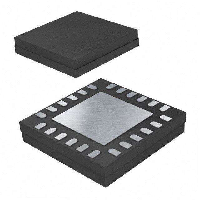
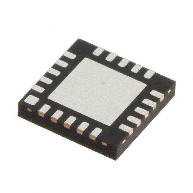
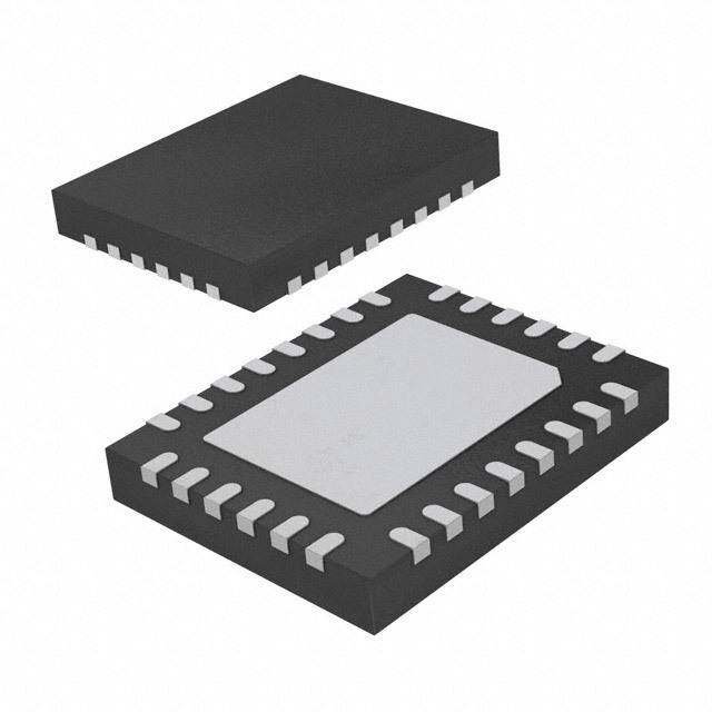
ICGOO电子元器件商城为您提供MW7IC2725NBR1由Freescale Semiconductor设计生产,在icgoo商城现货销售,并且可以通过原厂、代理商等渠道进行代购。 MW7IC2725NBR1价格参考。Freescale SemiconductorMW7IC2725NBR1封装/规格:RF 放大器, RF Amplifier IC WiMax 2.7GHz TO-272 WB-16。您可以下载MW7IC2725NBR1参考资料、Datasheet数据手册功能说明书,资料中有MW7IC2725NBR1 详细功能的应用电路图电压和使用方法及教程。
NXP USA Inc. 的 MW7IC2725NBR1 是一款射频(RF)放大器,属于高性能的宽带放大器,主要工作在中高频至微波频段。该器件基于氮化镓(GaN)技术,具备高功率密度、高效率和良好的热稳定性,适用于需要高线性度与输出功率的场景。

典型应用场景包括:
1. 无线通信基础设施:用于蜂窝基站中的功率放大阶段,支持4G LTE及5G网络部署,尤其适合宏基站和小基站中的射频前端模块。
2. 军事与国防系统:应用于雷达系统、电子战设备和通信干扰系统,因其高可靠性和宽频带性能,能够在严苛环境下稳定运行。
3. 工业与航空航天:用于卫星通信地面站、航电系统和远程无线传输设备,提供稳定的射频信号放大能力。
4. 测试与测量设备:作为信号发生器或放大模块的一部分,用于实验室环境中的高频信号测试与验证。

MW7IC2725NBR1 具有集成化设计和优良的散热性能,采用紧凑封装,便于系统集成。其高增益和低失真特性使其在多载波和复杂调制信号应用中表现优异,是现代高性能射频系统中的关键组件。
| 参数 | 数值 |
| 产品目录 | |
| 描述 | IC PWR AMP RF 2700MHZ TO-272-16 |
| 产品分类 | |
| 品牌 | Freescale Semiconductor |
| 数据手册 | |
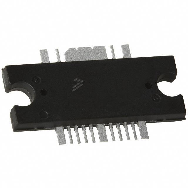
| 产品图片 |
|
| P1dB | 44dBm(25W) |
| 产品型号 | MW7IC2725NBR1 |
| RF类型 | WiMax |
| rohs | 无铅 / 符合限制有害物质指令(RoHS)规范要求 |
| 产品系列 | - |
| 供应商器件封装 | TO-272 WB-16 |
| 其它名称 | MW7IC2725NBR1-ND |
| 包装 | 带卷 (TR) |
| 噪声系数 | - |
| 增益 | 28.5dB |
| 封装/外壳 | TO-272-16 变式, 扁平引线 |
| 标准包装 | 500 |
| 测试频率 | 2.7GHz |
| 电压-电源 | 32V |
| 电流-电源 | 275mA |
| 频率 | 2.7GHz |


- 商务部:美国ITC正式对集成电路等产品启动337调查
- 曝三星4nm工艺存在良率问题 高通将骁龙8 Gen1或转产台积电
- 太阳诱电将投资9.5亿元在常州建新厂生产MLCC 预计2023年完工
- 英特尔发布欧洲新工厂建设计划 深化IDM 2.0 战略
- 台积电先进制程称霸业界 有大客户加持明年业绩稳了
- 达到5530亿美元!SIA预计今年全球半导体销售额将创下新高
- 英特尔拟将自动驾驶子公司Mobileye上市 估值或超500亿美元
- 三星加码芯片和SET,合并消费电子和移动部门,撤换高东真等 CEO
- 三星电子宣布重大人事变动 还合并消费电子和移动部门
- 海关总署:前11个月进口集成电路产品价值2.52万亿元 增长14.8%

PDF Datasheet 数据手册内容提取
Freescale Semiconductor Document Number: MW7IC2725N Technical Data Rev. 3, 1/2010 RF LDMOS Wideband Integrated Power Amplifiers MW7IC2725NR1 MW7IC2725GNR1 The MW7IC2725N wideband integrated circuit is designed with on-chip matching that makes it usable from 2300-2700 MHz. This multi-stage MW7IC2725NBR1 structure is rated for 26 to 32 Volt operation and covers all typical cellular base station modulation formats. • Typical WiMAX Performance: V = 28 Volts, I = 77 mA, I = 275 mA, DD DQ1 DQ2 P = 4 Watts Avg., f = 2700 MHz, OFDM 802.16d, 64 QAM 3/ , out 4 2500-2700 MHz, 4 W AVG., 28 V 4 Bursts, 10 MHz Channel Bandwidth, Input Signal PAR = 9.5 dB @ 0.01% WiMAX Probability on CCDF. (cid:2)Power Gain — 28.5 dB RF LDMOS WIDEBAND (cid:2)Power Added Efficiency — 17% INTEGRATED POWER AMPLIFIERS (cid:2)Device Output Signal PAR — 9 dB @ 0.01% Probability on CCDF (cid:2)ACPR @ 8.5 MHz Offset — -50 dBc in 1 MHz Channel Bandwidth Driver Applications • Typical WiMAX Performance: V = 28 Volts, I = 77 mA, I = 275 mA, CASE 1886-01 DD DQ1 DQ2 P = 26 dBm Avg., f = 2700 MHz, OFDM 802.16d, 64 QAM 3/ , TO-270 WB-16 out 4 4 Bursts, 10 MHz Channel Bandwidth, Input Signal PAR = 9.5 dB @ 0.01% PLASTIC Probability on CCDF. MW7IC2725NR1 (cid:2)Power Gain — 27.8 dB (cid:2)Power Added Efficiency — 3.2% (cid:2)Device Output Signal PAR — 9 dB @ 0.01% Probability on CCDF CASE 1887-01 (cid:2)ACPR @ 8.5 MHz Offset — -56 dBc in 1 MHz Channel Bandwidth TO-270 WB-16 GULL • Capable of Handling 10:1 VSWR, @ 32 Vdc, 2600 MHz, 40 Watts CW PLASTIC Output Power (3 dB Input Overdrive from Rated P ) out MW7IC2725GNR1 • Stable into a 5:1 VSWR. All Spurs Below -60 dBc @ 100 mW to 5 W CW P out • Typical P @ 1 dB Compression Point (cid:2) 25 Watts CW out Features CASE 1329-09 • 100% PAR Tested for Guaranteed Output Power Capability TO-272 WB-16 • Characterized with Series Equivalent Large-Signal Impedance Parameters PLASTIC MW7IC2725NBR1 and Common Source S-Parameters • On-Chip Matching (50 Ohm Input, DC Blocked) • Integrated Quiescent Current Temperature Compensation with Enable/Disable Function (1) • Integrated ESD Protection • 225°C Capable Plastic Package • RoHS Compliant • In Tape and Reel. R1 Suffix = 500 Units per 44 mm, 13 inch Reel. GND 1 16 GND VDNSC1 23 15 NC NC 4 NC 5 VDS1 RFin 6 14 RFout/VDS2 RFin RFout/VDS2 NC 7 VGS1 8 VGS2 9 VDS1 10 13 NC VGS1 Quiescent Current GND 11 12 GND VGS2 Temperature Compensation (1) (Top View) VDS1 Note: Exposed backside of the package is the source terminal for the transistors. Figure 1. Functional Block Diagram Figure 2. Pin Connections (cid:3)(cid:4)1. Refer to AN1977, Quiescent Current Thermal Tracking Circuit in the RF Integrated Circuit Family and to AN1987, Quiescent Current Control for the RF Integrated Circuit Device Family. Go to http://www.freescale.com/rf. Select Documentation/Application Notes - AN1977 or AN1987. © Freescale Semiconductor, Inc., 2008, 2010. All rights reserved. MW7IC2725NR1 MW7IC2725GNR1 MW7IC2725NBR1 RF Device Data Freescale Semiconductor 1
Table 1. Maximum Ratings Rating Symbol Value Unit Drain-Source Voltage VDS -0.5, +65 Vdc Gate-Source Voltage VGS -0.5, +10 Vdc Operating Voltage VDD 32, +0 Vdc Storage Temperature Range Tstg -(cid:5)65 to +150 °C Case Operating Temperature TC 150 °C Operating Junction Temperature (1,2) TJ 225 °C Input Power Pin 22 dBm Table 2. Thermal Characteristics Characteristic Symbol Value (2,3) Unit Thermal Resistance, Junction to Case RθJC °C/W WiMAX Application Stage 1, 28 Vdc, IDQ1 = 77 mA 5.9 (Case Temperature 75°C, Pout = 4 W Avg.) Stage 2, 28 Vdc, IDQ2 = 275 mA 1.4 CW Application Stage 1, 28 Vdc, IDQ1 = 77 mA 5.5 (Case Temperature 81°C, Pout = 25 W CW) Stage 2, 28 Vdc, IDQ2 = 275 mA 1.3 Table 3. ESD Protection Characteristics Test Methodology Class Human Body Model (per JESD22-A114) 1B (Minimum) Machine Model (per EIA/JESD22-A115) A (Minimum) Charge Device Model (per JESD22-C101) II (Minimum) Table 4. Moisture Sensitivity Level Test Methodology Rating Package Peak Temperature Unit Per JESD22-A113, IPC/JEDEC J-STD-020 3 260 °C Table 5. Electrical Characteristics (TA = 25°C unless otherwise noted) Characteristic Symbol Min Typ Max Unit Stage 1 - Off Characteristics Zero Gate Voltage Drain Leakage Current IDSS — — 10 μAdc (VDS = 65 Vdc, VGS = 0 Vdc) Zero Gate Voltage Drain Leakage Current IDSS — — 1 μAdc (VDS = 28 Vdc, VGS = 0 Vdc) Gate-Source Leakage Current IGSS — — 1 μAdc (VGS = 1.5 Vdc, VDS = 0 Vdc) Stage 1 - On Characteristics Gate Threshold Voltage VGS(th) 1.2 1.9 2.7 Vdc (VDS = 10 Vdc, ID = 20 μAdc) Gate Quiescent Voltage VGS(Q) — 2.7 — Vdc (VDS = 28 Vdc, IDQ1 = 77 mA) Fixture Gate Quiescent Voltage VGG(Q) 12.5 15.8 19.5 Vdc (VDD = 28 Vdc, IDQ1 = 77 mAdc, Measured in Functional Test) (cid:3)(cid:4)1. Continuous use at maximum temperature will affect MTTF. (cid:4)(cid:3)2. MTTF calculator available at http://www.freescale.com/rf. Select Software & Tools/Development Tools/Calculators to access MTTF calculators by product. (cid:4)(cid:3)3. Refer to AN1955, Thermal Measurement Methodology of RF Power Amplifiers. Go to http://www.freescale.com/rf. Select Documentation/Application Notes - AN1955. (continued) MW7IC2725NR1 MW7IC2725GNR1 MW7IC2725NBR1 RF Device Data 2 Freescale Semiconductor
Table 5. Electrical Characteristics (TA = 25°C unless otherwise noted) (continued) Characteristic Symbol Min Typ Max Unit Stage 2 - Off Characteristics Zero Gate Voltage Drain Leakage Current IDSS — — 10 μAdc (VDS = 65 Vdc, VGS = 0 Vdc) Zero Gate Voltage Drain Leakage Current IDSS — — 1 μAdc (VDS = 28 Vdc, VGS = 0 Vdc) Gate-Source Leakage Current IGSS — — 1 μAdc (VGS = 1.5 Vdc, VDS = 0 Vdc) Stage 2 - On Characteristics Gate Threshold Voltage VGS(th) 1.2 1.9 2.7 Vdc (VDS = 10 Vdc, ID = 80 μAdc) Gate Quiescent Voltage VGS(Q) — 2.7 — Vdc (VDS = 28 Vdc, IDQ2 = 275 mAdc) Fixture Gate Quiescent Voltage VGG(Q) 11 14 18 Vdc (VDD = 28 Vdc, IDQ2 = 275 mAdc, Measured in Functional Test) Drain-Source On-Voltage VDS(on) 0.15 0.47 0.8 Vdc (VGS = 10 Vdc, ID = 800 mAdc) Stage 2 - Dynamic Characteristics (1) Output Capacitance Coss — 111 — pF (VDS = 28 Vdc ± 30 mV(rms)ac @ 1 MHz, VGS = 0 Vdc) Functional Tests (In Freescale Test Fixture, 50 ohm system) VDD = 28 Vdc, IDQ1 = 77 mA, IDQ2 = 275 mA, Pout = 4 W Avg., f = 2700 MHz, WiMAX, OFDM 802.16d, 64 QAM 3/4, 4 Bursts, 10 MHz Channel Bandwidth, Input Signal PAR = 9.5 dB @ 0.01% Probability on CCDF. ACPR measured in 1 MHz Channel Bandwidth @ ±8.5 MHz Offset. Power Gain Gps 25.5 28.5 30.5 dB Power Added Efficiency PAE 15 17 — % Output Peak-to-Average Ratio @ 0.01% Probability on CCDF PAR — 9 — dB Adjacent Channel Power Ratio ACPR — -50 -46 dBc Input Return Loss IRL — -15 -10 dB Typical Performances OFDM Signal - 10 MHz Channel Bandwidth (In Freescale Test Fixture, 50 ohm system) VDD = 28 Vdc, IDQ1 = 77 mA, IDQ2 = 275 mA, Pout = 4 W Avg., f = 2700 MHz, WiMAX, OFDM 802.16d, 64 QAM 3/4, 4 Bursts, 10 MHz Channel Bandwidth, Input Signal PAR = 9.5 dB @ 0.01% Probability on CCDF. Relative Constellation Error (2) RCE — -33 — dB Error Vector Magnitude (2) EVM — 2.2 — % rms (cid:3)(cid:4)1. Part internally matched both on input and output. (continued) (cid:4)(cid:3)2. RCE = 20Log(EVM/100) MW7IC2725NR1 MW7IC2725GNR1 MW7IC2725NBR1 RF Device Data Freescale Semiconductor 3
Table 5. Electrical Characteristics (TA = 25°C unless otherwise noted) (continued) Characteristic Symbol Min Typ Max Unit Typical Performances (In Freescale Test Fixture, 50 ohm system) VDD = 28 Vdc, IDQ1 = 77 mA, IDQ2 = 275 mA, 2500-2700 MHz Bandwidth Pout @ 1 dB Compression Point, CW P1dB — 25 — W IMD Symmetry @ 27 W PEP, Pout where IMD Third Order IMDsym MHz Intermodulation (cid:3) 30 dBc — 50 — (Delta IMD Third Order Intermodulation between Upper and Lower Sidebands > 2 dB) VBW Resonance Point VBWres — 90 — MHz (IMD Third Order Intermodulation Inflection Point) Gain Flatness in 200 MHz Bandwidth @ Pout = 4 W Avg. GF — 0.5 — dB Average Deviation from Linear Phase in 200 MHz Bandwidth Φ — 2.1 — ° @ Pout = 25 W CW Average Group Delay @ Pout = 25 W CW, f = 2600 MHz Delay — 2.3 — ns Part-to-Part Insertion Phase Variation @ Pout = 25 W CW, ΔΦ — 22 — ° f = 2600 MHz, Six Sigma Window Gain Variation over Temperature ΔG — 0.036 — dB/°C (-30°C to +85°C) Output Power Variation over Temperature ΔP1dB — 0.003 — dBm/°C (-30°C to +85°C) Typical Driver Performances (In Freescale Test Fixture, 50 ohm system) VDD = 28 Vdc, IDQ1 = 77 mA, IDQ2 = 275 mA, Pout = 26 dBm Avg., f = 2700 MHz, WiMAX, OFDM 802.16d, 64 QAM 3/4, 4 Bursts, 10 MHz Channel Bandwidth, Input Signal PAR = 9.5 dB @ 0.01% Probability on CCDF. ACPR measured in 1 MHz Channel Bandwidth @ ±8.5 MHz Offset. Power Gain Gps — 27.8 — dB Power Added Efficiency PAE — 3.2 — % Output Peak-to-Average Ratio @ 0.01% Probability on CCDF PAR — 9 — dB Adjacent Channel Power Ratio ACPR — -56 — dBc Input Return Loss IRL — -13 — dB Relative Constellation Error @ Pout = 1.25 W Avg. (1) RCE — -40 — dB (cid:3)(cid:4)1. RCE = 20Log(EVM/100) MW7IC2725NR1 MW7IC2725GNR1 MW7IC2725NBR1 RF Device Data 4 Freescale Semiconductor
VDD1 VD2 B1 28 V C17 C16 C9 C15 C8 C14 C7 1 NC DUT NC 16 C13 C12 2 NC 15 3 NC 4 NC Z13 RF 5 NC RF INPUT OUTPUT Z1 Z2 Z3 Z4 14 Z5 Z6 Z7 Z8 Z9 Z10 Z11 Z12 Z14 6 C11 C4 7 NC C10 8 Quiescent Current C5 9 Temperature 10 Compensation NC 13 11 NC NC 12 C6 C1 VG1 C2 R4 R5 R6 C3 VG2 R1 R2 R3 Z1 0.500″ x 0.027″ Microstrip Z9 0.040″ x 0.061″ Microstrip Z2 0.075″ x 0.127″ Microstrip Z10 0.020″ x 0.050″ Microstrip Z3 1.640″ x 0.027″ Microstrip Z11 0.050″ x 0.050″ Microstrip Z4 0.100″ x 0.042″ Microstrip Z12 0.050″ x 0.027″ Microstrip Z5 0.151″ x 0.268″ Microstrip Z13* 0.338″ x 0.020″ Microstrip Z6 0.025″ x 0.268″ x 0.056″ Taper Z14 1.551″ x 0.027″ Microstrip Z7 0.050″ x 0.056″ Microstrip PCB Rogers R04350B, 0.0133″, εr = 3.48 Z8 0.356″ x 0.056″ Microstrip * Line length includes microstrip bends Figure 3. MW7IC2725NR1(GNR1)(NBR1) Test Circuit Schematic Table 6. MW7IC2725NR1(GNR1)(NBR1) Test Circuit Component Designations and Values Part Description Part Number Manufacturer B1 47 Ω, 100 MHz Short Ferrite Bead 2743019447 Fair-Rite C1, C4, C7, C12, C15 6.8 pF Chip Capacitors ATC600S6R8CT250XT ATC C2, C5, C8, C13 10 nF Chip Capacitors C0603C103J5RAC Kemet C3, C6, C9, C14 1 μF, 50 V Chip Capacitors GRM32RR71H105KA01B Murata C10 2.4 pF Chip Capacitor ATC600S2R4BT250XT ATC C11 3.3 pF Chip Capacitor ATC600S3R3BT250XT ATC C16, C17 10 μF, 50 V Chip Capacitors GRM55DR61H106KA88B Murata R1, R4 12 KΩ, 1/4 W Chip Resistors CRCW12061202FKEA Vishay R2, R3, R5, R6 1 KΩ, 1/4 W Chip Resistors CRCW12061001FKEA Vishay MW7IC2725NR1 MW7IC2725GNR1 MW7IC2725NBR1 RF Device Data Freescale Semiconductor 5
MW7IC2725N Rev. 1.3 B1 C16 C17 C15 C8 C9 C14 C12 C7 C13 C4 A C5 RE C1 A C10 C11 R4 R5 R6 C2 T U O T U VG1 C6 C C3 R1 R2 R3 VG2 Figure 4. MW7IC2725NR1(GNR1)(NBR1) Test Circuit Component Layout MW7IC2725NR1 MW7IC2725GNR1 MW7IC2725NBR1 RF Device Data 6 Freescale Semiconductor
TYPICAL CHARACTERISTICS 28.6 18 D PAE DE%) 28.4 17 ADY ( R C 28.2 Gps 16 WEEN R GAIN (dB) 22772..886 VOBaDFnDDd =Mw 2 i8d80t hV2,. d1Inc6,pd Pu, to6 Su4ti g=Qn 4Aa MlW P 3A(/AR4v, =g4 . 9)B,. 5uID rdsQBt1s ,=@ 1 70 07 M. 0mH1A%z, C IPDhrQao2nb =naeb 2lil7it5y mA 1-15543 PAE, POEFFICI -16 dB) -0.2 WE on CCDF S ( O 27.4 -54 -18 OS -0.4 G, Pps 22762..728 PAACRPCR ---555567 ACPR (dBc) ---222402 T RETURN L ---100..68 PARC (dB) U 26.6 IRL -58 -26 NP -1.2 2500 2525 2550 2575 2600 2625 2650 2675 2700 RL, I I f, FREQUENCY (MHz) Figure 5. WiMAX Broadband Performance @ P = 4 Watts Avg. out 28.6 3.5 D DE%) 28.4 PAE 3 ADY ( 28.2 Gps 2.5 ER NC WE OCI B) 28 2 PFI OWER GAIN (d 222777...864 OVInDFpDDu t=M S 2 i8g80nP V2aA.dl1 RcP6C,Ad PR, o6 u=4t =9Q. 52A 6Md Bd 3B @/m4, 04(A. 0Bv1gu%.r)s, t PsID,r oQ1b10a =Mb i7Hli7tzy mConAh ,aC InDCnQDe2lF B= a2n7d5w midAth --155.567 PAE, EF --1105 LOSS (dB) --00..24 G, Pps 22762..728 ACPR ---556890 ACPR (dBc) ---322005 UT RETURN ---100..68 PARC (dB) IRL NP 26.6 -61 -35 L, I -1.2 2500 2525 2550 2575 2600 2625 2650 2675 2700 R I f, FREQUENCY (MHz) Figure 6. WiMAX Broadband Performance @ P = 26 dBm Avg. out 30 30 IDQ2 = 412 mA IDQ1 = 103 mA 29 29 344 mA 96 mA B) 28 275 mA B) 28 77 mA d d N ( N ( GAI 27 GAI 27 R 206 mA R 58 mA E E W 26 W 26 O O P P G, ps25 137 mA G, ps25 39 mA VDD = 28 Vdc VDD = 28 Vdc 24 IDQ1 = 77 mA 24 IDQ2 = 275 mA f = 2600 MHz f = 2600 MHz 23 23 0.1 1 10 100 0.1 1 10 100 Pout, OUTPUT POWER (WATTS) CW Pout, OUTPUT POWER (WATTS) CW Figure 7. Power Gain versus Output Power Figure 8. Power Gain versus Output Power @ I = 77 mA @ I = 275 mA DQ1 DQ2 MW7IC2725NR1 MW7IC2725GNR1 MW7IC2725NBR1 RF Device Data Freescale Semiconductor 7
TYPICAL CHARACTERISTICS 0 Bc) VDD = 28 Vdc, Pout = 27 W (PEP), IDQ1 = 77 mA d N ( -10 IDQ2 = 275 mA, Two-Tone Measurements O (f1 + f2)/2 = Center Frequency of 2600 MHz TI R TO -20 S DI N IM3-U O -30 ATI IM3-L L U IM5-L OD -40 M IM5-U R E IM7-L T -50 N D, I IM7-U M I -60 1 10 100 TWO-TONE SPACING (MHz) Figure 9. Intermodulation Distortion Products versus Tone Spacing 29 1 35 -30 VDD = 28 Vdc, IDQ1 = 77 mA, IDQ2 = 275 mA f = 2600 MHz, OFDM 802.16d, 64 QAM 3/4, 4 Bursts, 10 MHz Channel %) WER GAIN (dB) 22872..855 PRESSION AT 0.01%TY ON CCDF (dB) --120 -1 B(cid:2)daB n = dPw 4roi.d0bth1a,b WIinlitpyu ot nS CigCnaDl FPAR = 9.5 dB @ 0.01% PAEGpsACPR 322050 ADDED EFICIENCY ( ---344505 CPR (dBc) G, POps 262.75 UTPUT COMPROBABILI --34 PARC 1150 AE, POWER --5505 A O -2 dB = 6.21 W -3 dB = 8.59 W P 26 -5 5 -60 1 3 6 9 12 15 Pout, OUTPUT POWER (WATTS) Figure 10. Output Peak-to-Average Ratio Compression (PARC) versus Output Power 45 -15 ENCY (%),B) 4305 Vf1P =0AD DRM2 6 =H=0 2z09 8 .CM5 Vh HddaBzcn, ,n @ OIeDlF Q0BD1.a0 M=n1 d%78w70 Pi 2dmr.t1ohA6b,, da IIn,bD p6iQlui4t2yt Q =So Ain2gM 7nC5a C3 lm/D4,AF 4 Bursts -40(cid:2)28C8555(cid:2)(cid:2)(cid:2)CCC --2205 FFICIAIN (d 30 25(cid:2)C -30 OWER ADDED EG, POWER Gps221505 TC = -40(cid:2)CPA2E5(cid:2)C 85(cid:2)C Gps -40(cid:2)C ---344505 ACPR (dBc) P 10 -50 AE, ACPR P 5 -55 0 -60 1 10 50 Pout, OUTPUT POWER (WATTS) AVG. WiMAX Figure 11. WiMAX, ACPR, Power Gain and Power Added Efficiency versus Output Power MW7IC2725NR1 MW7IC2725GNR1 MW7IC2725NBR1 RF Device Data 8 Freescale Semiconductor
TYPICAL CHARACTERISTICS 25 0 109 S21 19 -10 108 1st Stage 13 -20 S) 107 R B) B) U d d O 2nd Stage S21 ( 7 -30 S11 ( TF (H 106 T S11 M 1 -40 105 VDD = 28 Vdc IDQ1 = 77 mA, IDQ2 = 275 mA -5 -50 104 1800 2000 2200 2400 2600 2800 3000 3200 3400 90 110 130 150 170 190 210 230 250 f, FREQUENCY (MHz) TJ, JUNCTION TEMPERATURE (°C) Figure 12. Broadband Frequency Response This above graph displays calculated MTTF in hours when the device is operated at VDD = 28 Vdc, Pout = 4 W Avg., and PAE = 17%. MTTF calculator available at http://www.freescale.com/rf. Select Software & Tools/Development Tools/Calculators to access MTTF calculators by product. Figure 13. MTTF versus Junction Temperature WIMAX TEST SIGNAL 100 -10 10 MHz -20 10 Channel BW Input Signal -30 %) 1 TY ( -40 LI 0.1 BI BA B) -50 O d R 0.01 ( P OFDM 802.16d, 64 QAM 3/4, 4 Bursts -60 10 MHz Channel Bandwidth, Input Signal 0.001 PAR = 9.5 dB @ 0.01% Probability -70 on CCDF 0.0001 0 2 4 6 8 10 -80 ACPR in 1 MHz ACPR in 1 MHz PEAK-TO-AVERAGE (dB) Integrated BW Integrated BW -90 Figure 14. OFDM 802.16d Test Signal -20 -15 -10 -5 0 5 10 15 20 f, FREQUENCY (MHz) Figure 15. WiMAX Spectrum Mask Specifications MW7IC2725NR1 MW7IC2725GNR1 MW7IC2725NBR1 RF Device Data Freescale Semiconductor 9
Zo = 50 Ω f = 2700 MHz f = 2700 MHz Zload Zsource f = 2500 MHz f = 2500 MHz VDD = 28 Vdc, IDQ1 = 77 mA, IDQ2 = 275 mA, Pout = 4 W Avg. f Zsource Zload MHz (cid:2) (cid:2) 2500 36.381 - j4.271 5.717 - j3.618 2525 36.041 - j3.328 5.624 - j3.187 2550 35.753 - j2.363 5.578 - j2.770 2575 35.516 - j1.380 5.589 - j2.412 2600 35.333 - j0.381 5.586 - j2.088 2625 35.203 + j0.635 5.579 - j1.807 2650 35.126 + j1.664 5.552 - j1.559 2675 35.104 + j2.707 5.564 - j1.335 2700 35.138 + j3.760 5.568 - j1.164 Zsource = Test circuit impedance as measured from gate to ground. Zload = Test circuit impedance as measured from drain to ground. Input Device Output Matching Under Matching Network Test Network Z Z source load Figure 16. Series Equivalent Source and Load Impedance MW7IC2725NR1 MW7IC2725GNR1 MW7IC2725NBR1 RF Device Data 10 Freescale Semiconductor
Table 7. Common Source S-Parameters (VDD = 28 V, IDQ1 = 77 mA, IDQ2 = 275 mA, TC = 25°C, 50 Ohm System) S11 S21 S12 S22 f MHz |S11| ∠(cid:4)φ |S21| ∠(cid:4)φ |S12| ∠(cid:4)φ |S22| ∠(cid:4)φ 1500 0.735 61.0 0.001 -167.6 0.000501 26.6 0.992 167.9 1550 0.729 53.3 0.004 -146.0 0.000361 34.7 0.993 166.3 1600 0.715 46.5 0.014 -146.4 0.000114 109.5 0.991 164.6 1650 0.695 39.8 0.039 -152.5 0.000385 148.4 0.992 162.7 1700 0.665 32.9 0.110 -166.8 0.000773 155.6 0.989 160.5 1750 0.619 25.0 0.299 169.4 0.00134 153.2 0.979 157.8 1800 0.549 15.1 0.708 134.4 0.00198 143.0 0.944 155.2 1850 0.452 2.6 1.335 96.3 0.00250 131.2 0.903 153.9 1900 0.332 -14.4 2.195 62.1 0.00290 121.7 0.879 153.0 1950 0.199 -40.1 3.445 32.7 0.00320 113.8 0.847 151.0 2000 0.089 -91.9 5.724 4.8 0.00345 108.5 0.817 147.7 2050 0.078 167.4 10.041 -26.2 0.00382 107.0 0.749 140.6 2100 0.116 90.3 19.072 -65.1 0.00525 105.3 0.571 125.2 2150 0.170 -13.2 32.642 -126.0 0.00781 77.9 0.054 160.2 2200 0.192 -93.2 31.339 171.3 0.00640 41.0 0.555 -144.4 2250 0.177 -123.0 26.174 130.3 0.00432 24.9 0.726 -160.3 2300 0.163 -132.6 23.605 98.7 0.00294 22.3 0.770 -167.1 2350 0.153 -140.5 22.427 70.0 0.00224 31.0 0.789 -170.1 2400 0.119 -153.6 21.922 41.7 0.00208 42.5 0.800 -171.0 2450 0.059 -165.3 21.172 14.2 0.00216 48.9 0.820 -171.2 2500 0.014 -50.7 20.172 -12.5 0.00227 48.9 0.850 -171.3 2550 0.055 -55.0 19.222 -39.5 0.00213 51.4 0.889 -171.7 2600 0.056 -84.7 17.366 -66.8 0.00209 57.8 0.933 -173.2 2650 0.029 177.4 14.562 -91.5 0.00247 65.6 0.961 -175.8 2700 0.069 103.3 12.199 -111.7 0.00286 62.2 0.968 -178.0 2750 0.122 84.1 10.485 -130.4 0.00308 56.3 0.969 -179.5 2800 0.287 59.8 8.086 -154.4 0.00326 50.9 0.969 179.3 2850 0.184 -5.4 7.102 -152.5 0.00292 39.2 0.966 178.6 2900 0.129 -17.4 6.753 -169.3 0.00256 38.6 0.969 178.0 2950 0.128 -41.0 6.107 175.4 0.00232 38.5 0.970 177.4 3000 0.164 -65.7 5.445 160.8 0.00213 39.9 0.972 176.9 3050 0.223 -86.2 4.867 146.7 0.00196 42.0 0.972 176.4 3100 0.297 -100.4 4.363 133.2 0.00183 46.0 0.973 176.0 3150 0.374 -110.4 3.918 120.0 0.00176 51.4 0.974 175.5 3200 0.447 -118.0 3.534 107.2 0.00181 56.5 0.974 174.9 3250 0.515 -123.4 3.198 95.3 0.00191 60.9 0.975 174.3 3300 0.563 -128.0 2.951 83.3 0.00211 58.8 0.975 173.7 3350 0.619 -131.8 2.761 71.2 0.00206 63.0 0.976 173.0 3400 0.651 -136.0 2.581 58.8 0.00218 64.8 0.975 172.3 3450 0.671 -140.1 2.418 46.0 0.00237 68.3 0.975 171.6 (continued) MW7IC2725NR1 MW7IC2725GNR1 MW7IC2725NBR1 RF Device Data Freescale Semiconductor 11
Table 7. Common Source S-Parameters (VDD = 28 V, IDQ1 = 77 mA, IDQ2 = 275 mA, TC = 25°C, 50 Ohm System) (continued) S11 S21 S12 S22 f MHz |S11| ∠(cid:4)φ |S21| ∠(cid:4)φ |S12| ∠(cid:4)φ |S22| ∠(cid:4)φ 3500 0.679 -144.4 2.257 32.6 0.00265 68.5 0.974 171.0 3550 0.677 -147.9 2.054 19.2 0.00280 65.0 0.976 170.5 3600 0.661 -153.5 1.851 5.0 0.00281 67.1 0.976 170.0 3650 0.696 -153.8 1.644 -5.8 0.00328 69.3 0.976 169.6 3700 0.721 -161.3 1.453 -19.4 0.00350 65.8 0.977 169.4 3750 0.737 -168.1 1.243 -32.1 0.00357 64.5 0.978 169.2 3800 0.753 -174.7 1.042 -43.7 0.00374 64.5 0.979 169.2 3850 0.771 179.2 0.859 -54.3 0.00401 62.5 0.980 169.2 3900 0.788 174.4 0.708 -62.8 0.00407 58.4 0.980 169.3 3950 0.812 169.8 0.583 -71.5 0.00416 57.7 0.981 169.3 4000 0.829 166.0 0.477 -79.0 0.00427 55.8 0.982 169.3 MW7IC2725NR1 MW7IC2725GNR1 MW7IC2725NBR1 RF Device Data 12 Freescale Semiconductor
ALTERNATIVE PEAK TUNE LOAD PULL CHARACTERISTICS 50 50 P3dB = 45.73 dBm (36 W) Ideal P3dB = 44.46 dBm (35 W) Ideal 48 48 P1dB = 45.42 dBm (28 W) m) 46 P1dB = 44.61 dBm (29 W) m) 46 B B ER (d 44 Actual ER (d 44 Actual W W 42 O O P 42 P T T 40 U U P 40 P UT UT 38 O O P, out 38 VDD = 28 Vdc, IDQ1 = 77 mA, IDQ2 = 275 mA P, out 36 VDD = 28 Vdc, IDQ1 = 77 mA, IDQ2 = 275 mA 36 Pulsed CW, 10 μsec(on), 10% Duty Cycle, 34 Pulsed CW, 10 μsec(on), 10% Duty Cycle, f = 2500 MHz f = 2700 MHz 34 32 3 4 5 6 7 8 9 10 11 12 13 14 15 16 17 18 19 2 3 4 5 6 7 8 9 10 11 12 13 14 15 16 17 18 19 20 Pin, INPUT POWER (dBm) Pin, INPUT POWER (dBm) NOTE: Load Pull Test Fixture Tuned for Peak P1dB Output Power @ 28 V NOTE: Load Pull Test Fixture Tuned for Peak P1dB Output Power @ 28 V Test Impedances per Compression Level Test Impedances per Compression Level Zsource Zload Zsource Zload Ω Ω Ω Ω P1dB 42.7 + j11.6 4.86 - j1.63 P1dB 39.5 - j8.7 3.53 - j1.66 Figure 17. Pulsed CW Output Power Figure 18. Pulsed CW Output Power versus Input Power @ 28 V @ 2500 MHz versus Input Power @ 28 V @ 2700 MHz MW7IC2725NR1 MW7IC2725GNR1 MW7IC2725NBR1 RF Device Data Freescale Semiconductor 13
PACKAGE DIMENSIONS MW7IC2725NR1 MW7IC2725GNR1 MW7IC2725NBR1 RF Device Data 14 Freescale Semiconductor
MW7IC2725NR1 MW7IC2725GNR1 MW7IC2725NBR1 RF Device Data Freescale Semiconductor 15
MW7IC2725NR1 MW7IC2725GNR1 MW7IC2725NBR1 RF Device Data 16 Freescale Semiconductor
MW7IC2725NR1 MW7IC2725GNR1 MW7IC2725NBR1 RF Device Data Freescale Semiconductor 17
MW7IC2725NR1 MW7IC2725GNR1 MW7IC2725NBR1 RF Device Data 18 Freescale Semiconductor
MW7IC2725NR1 MW7IC2725GNR1 MW7IC2725NBR1 RF Device Data Freescale Semiconductor 19
MW7IC2725NR1 MW7IC2725GNR1 MW7IC2725NBR1 RF Device Data 20 Freescale Semiconductor
MW7IC2725NR1 MW7IC2725GNR1 MW7IC2725NBR1 RF Device Data Freescale Semiconductor 21
MW7IC2725NR1 MW7IC2725GNR1 MW7IC2725NBR1 RF Device Data 22 Freescale Semiconductor
PRODUCT DOCUMENTATION, TOOLS AND SOFTWARE Refer to the following documents to aid your design process. Application Notes • AN1907: Solder Reflow Attach Method for High Power RF Devices in Plastic Packages • AN1955: Thermal Measurement Methodology of RF Power Amplifiers • AN1977: Quiescent Current Thermal Tracking Circuit in the RF Integrated Circuit Family • AN1987: Quiescent Current Control for the RF Integrated Circuit Device Family • AN3263: Bolt Down Mounting Method for High Power RF Transistors and RFICs in Over-Molded Plastic Packages • AN3789: Clamping of High Power RF Transistors and RFICs in Over-Molded Plastic Packages Engineering Bulletins • EB212: Using Data Sheet Impedances for RF LDMOS Devices Software • Electromigration MTTF Calculator • RF High Power Model For Software and Tools, do a Part Number search at http://www.freescale.com, and select the “Part Number” link. Go to the Software & Tools tab on the part's Product Summary page to download the respective tool. REVISION HISTORY The following table summarizes revisions to this document. Revision Date Description 0 June 2008 • Initial Release of Data Sheet 1 July 2008 • Added MW7IC2725NBR1 device and corresponding case outline information to data sheet. 2 Oct. 2008 • Added Fig. 13, MTTF versus Junction Temperature, p. 9 3 Jan. 2010 • Modified VSWR rating to show the 3 dB overdrive capability, p. 1 • Maximum Ratings table: Added Case Operating Temperature and set limit to 150°C. Corrected maximum input power level to the tested value from 20 dBm to 22 dBm, p. 2 • Added AN3789, Clamping of High Power RF Transistors and RFICs in Over-Molded Plastic Packages to Product Documentation, Application Notes, p. 23 MW7IC2725NR1 MW7IC2725GNR1 MW7IC2725NBR1 RF Device Data Freescale Semiconductor 23
How to Reach Us: Home Page: www.freescale.com Web Support: http://www.freescale.com/support USA/Europe or Locations Not Listed: Freescale Semiconductor, Inc. Technical Information Center, EL516 2100 East Elliot Road Tempe, Arizona 85284 1-800-521-6274 or +1-480-768-2130 www.freescale.com/support Europe, Middle East, and Africa: Freescale Halbleiter Deutschland GmbH Information in this document is provided solely to enable system and software Technical Information Center implementers to use Freescale Semiconductor products. There are no express or Schatzbogen 7 81829 Muenchen, Germany implied copyright licenses granted hereunder to design or fabricate any integrated +44 1296 380 456 (English) circuits or integrated circuits based on the information in this document. +46 8 52200080 (English) +49 89 92103 559 (German) Freescale Semiconductor reserves the right to make changes without further notice to +33 1 69 35 48 48 (French) any products herein. Freescale Semiconductor makes no warranty, representation or www.freescale.com/support guarantee regarding the suitability of its products for any particular purpose, nor does Freescale Semiconductor assume any liability arising out of the application or use of Japan: any product or circuit, and specifically disclaims any and all liability, including without Freescale Semiconductor Japan Ltd. Headquarters limitation consequential or incidental damages. “Typical” parameters that may be ARCO Tower 15F provided in Freescale Semiconductor data sheets and/or specifications can and do 1-8-1, Shimo-Meguro, Meguro-ku, vary in different applications and actual performance may vary over time. All operating Tokyo 153-0064 parameters, including “Typicals”, must be validated for each customer application by Japan customer's technical experts. Freescale Semiconductor does not convey any license 0120 191014 or +81 3 5437 9125 under its patent rights nor the rights of others. Freescale Semiconductor products are support.japan@freescale.com not designed, intended, or authorized for use as components in systems intended for surgical implant into the body, or other applications intended to support or sustain life, Asia/Pacific: Freescale Semiconductor China Ltd. or for any other application in which the failure of the Freescale Semiconductor product Exchange Building 23F could create a situation where personal injury or death may occur. Should Buyer No. 118 Jianguo Road purchase or use Freescale Semiconductor products for any such unintended or Chaoyang District unauthorized application, Buyer shall indemnify and hold Freescale Semiconductor Beijing 100022 and its officers, employees, subsidiaries, affiliates, and distributors harmless against all China claims, costs, damages, and expenses, and reasonable attorney fees arising out of, +86 10 5879 8000 directly or indirectly, any claim of personal injury or death associated with such support.asia@freescale.com unintended or unauthorized use, even if such claim alleges that Freescale For Literature Requests Only: Semiconductor was negligent regarding the design or manufacture of the part. Freescale Semiconductor Literature Distribution Center 1-800-441-2447 or +1-303-675-2140 Freescale(cid:3) and the Freescale logo are trademarks of Freescale Semiconductor, Inc. Fax: +1-303-675-2150 All other product or service names are the property of their respective owners. LDCForFreescaleSemiconductor@hibbertgroup.com © Freescale Semiconductor, Inc. 2008, 2010. All rights reserved. MW7IC2725NR1 MW7IC2725GNR1 MW7IC2725NBR1 Document Number: MW7IC2725N RF Device Data 2R4ev. 3, 1/2010 Freescale Semiconductor