 Datasheet下载
- 型号: UCLAMP3304A.TCT
- 制造商: SEMTECH
- 库位|库存: xxxx|xxxx
- 要求:
| 数量阶梯 | 香港交货 | 国内含税 |
| +xxxx | $xxxx | ¥xxxx |
查看当月历史价格
查看今年历史价格
UCLAMP3304A.TCT产品简介:
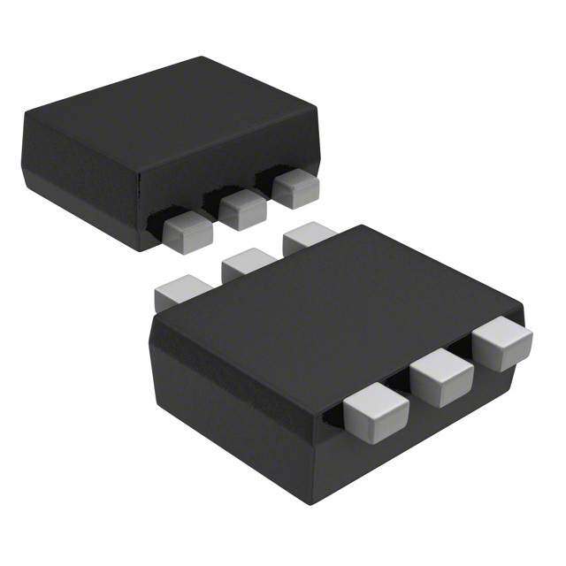
ICGOO电子元器件商城为您提供UCLAMP3304A.TCT由SEMTECH设计生产,在icgoo商城现货销售,并且可以通过原厂、代理商等渠道进行代购。 UCLAMP3304A.TCT价格参考¥1.92-¥2.16。SEMTECHUCLAMP3304A.TCT封装/规格:TVS - 二极管, 8V Clamp 5A (8/20µs) Ipp Tvs Diode Surface Mount SC-89-6。您可以下载UCLAMP3304A.TCT参考资料、Datasheet数据手册功能说明书,资料中有UCLAMP3304A.TCT 详细功能的应用电路图电压和使用方法及教程。
UCLAMP3304A.TCT是Semtech Corporation推出的一款瞬态电压抑制(TVS)二极管,属于高性能的静电放电(ESD)保护器件。该器件主要用于保护敏感电子元件免受瞬态电压脉冲和静电放电的损害。

其典型应用场景包括:便携式消费类电子产品,如智能手机、平板电脑、笔记本电脑和可穿戴设备,用于保护USB接口、HDMI端口、音频插孔等高速数据线路;通信设备中的以太网端口、传感器接口和射频模块;以及工业控制系统的信号线和数据传输端口。UCLAMP3304A.TCT具有低电容特性(通常低于1pF),可确保对高速信号完整性影响最小,适用于高频信号线路的保护。

此外,该器件采用小型化封装(如DFN1006-2),节省PCB空间,适合高密度布局设计。其钳位电压低、响应速度快(皮秒级),能有效将浪涌电压限制在安全范围内,保护后级集成电路。工作温度范围宽(-40°C至+85°C),适应多种环境条件。

综上,UCLAMP3304A.TCT广泛应用于需要高可靠性ESD防护的消费电子、通信和工业领域,特别适合高速、低功耗、小型化的现代电子系统。
| 参数 | 数值 |
| 产品目录 | |
| 描述 | TVS DIODE 3.3VWM 8VC SC896 |
| 产品分类 | |
| 品牌 | Semtech |
| 数据手册 | |
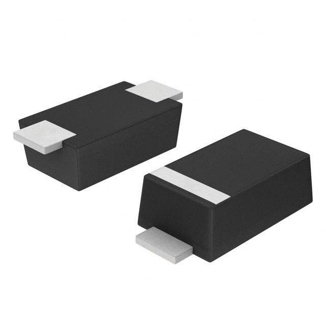
| 产品图片 |
|
| 产品型号 | UCLAMP3304A.TCT |
| rohs | 无铅 / 符合限制有害物质指令(RoHS)规范要求 |
| 产品系列 | uClamp™ |
| 不同频率时的电容 | 22pF @ 1MHz |
| 产品目录页面 | |
| 供应商器件封装 | SC-89-6 |
| 其它名称 | UCLAMP3304ATCT |
| 功率-峰值脉冲 | 40W |
| 包装 | 带卷 (TR) |
| 单向通道 | 4 |
| 双向通道 | - |
| 安装类型 | 表面贴装 |
| 封装/外壳 | SOT-563,SOT-666 |
| 工作温度 | -55°C ~ 125°C |
| 应用 | 通用 |
| 标准包装 | 3,000 |
| 电压-击穿(最小值) | 3.5V |
| 电压-反向关态(典型值) | 3.3V (最小值) |
| 电压-箝位(最大值)@Ipp | 8V |
| 电流-峰值脉冲(10/1000µs) | 5A (8/20µs) |
| 电源线路保护 | 无 |
| 类型 | 齐纳 |


- 商务部:美国ITC正式对集成电路等产品启动337调查
- 曝三星4nm工艺存在良率问题 高通将骁龙8 Gen1或转产台积电
- 太阳诱电将投资9.5亿元在常州建新厂生产MLCC 预计2023年完工
- 英特尔发布欧洲新工厂建设计划 深化IDM 2.0 战略
- 台积电先进制程称霸业界 有大客户加持明年业绩稳了
- 达到5530亿美元!SIA预计今年全球半导体销售额将创下新高
- 英特尔拟将自动驾驶子公司Mobileye上市 估值或超500亿美元
- 三星加码芯片和SET,合并消费电子和移动部门,撤换高东真等 CEO
- 三星电子宣布重大人事变动 还合并消费电子和移动部门
- 海关总署:前11个月进口集成电路产品价值2.52万亿元 增长14.8%


PDF Datasheet 数据手册内容提取
uClamp3304A µClampTM 4-Line ESD protection Array PPRROOTTEECCTTIIOONN PPRROODDUUCCTTSS - MicroClampTM Description Features The µClampTM series of TVS arrays are designed to pro- (cid:139) Transient protection for data lines to tect sensitive electronics from damage or latch-up due IEC 61000-4-2 (ESD) ±15kV (air), ±8kV (contact) to ESD. They are designed for use in applications where IEC 61000-4-4 (EFT) 40A (5/50ns) board space is at a premium. Each device requires less (cid:139) Protects four unidirectional I/O lines than 2.9mm2 of PCB area and will protect up to four (cid:139) Ultra-small SC-89 package (11111.....77777 xxxxx 11111.....77777 xxxxx 00000.....66666mmmmmmmmmm) lines. They are unidirectional devices and may be used requires less than 2.9mm2 of PCB area on lines with positive signal polarities. (cid:139) Working voltage: 3.3V The µclampTM3304A is constructed using Semtech’s pro- (cid:139) Low leakage current prietary EPD process technology. The EPD process pro- (cid:139) Low operating and clamping voltages vides low standoff voltages with significant reductions in (cid:139) Solid-state silicon-avalanche technology leakage currents and capacitance over silicon-avalanche diode processes. They feature a true operating voltage Mechanical Characteristics of 3.3 volts for superior protection when compared to (cid:139) SC-89 (SOT-666) package traditional pn junction devices. (cid:139) Molding compound flammability rating: UL 94V-0 These devices may be used to meet the immunity re- (cid:139) Marking: Marking Code quirements of IEC 61000-4-2, level 4. They offer desir- (cid:139) Lead Finish: Matte Tin able characteristics for board level protection including (cid:139) RoHS Compliant fast response time, low operating and clamping voltage, (cid:139) Weight: 2.9mg (typical) and no device degradation. The small SC89 package makes them ideal for use in portable electronics such as (cid:139) Packaging: Tape and Reel cell phones, PDAs, notebook computers, and digital cam- Applications eras. (cid:139) Cellular Handsets and Accessories (cid:139) Cordless Phones (cid:139) Notebooks and Handhelds (cid:139) Portable Instrumentation (cid:139) Digital Cameras (cid:139) Peripherals (cid:139) MP3 Players Dimensions Schematic & PIN Configuration 1.70 0.50 1.25 1.70 0.30 0.60 Maximum Dimensions (mm) SC-89 (Top View) Revision 01/18/08 1 www.semtech.com
µClamp3304A PROTECTION PRODUCTS Absolute Maximum Rating Rating Symbol Value Units PeakPulsePower(tp =8/20µs) P 40 Watts pk MaximumPeakPulseCurrent (tp =8/20µs) I 5 Amps pp ESDperIEC61000-4-2 (Air) V +/- 20 kV PP ESDperIEC61000-4-2 (Contact) +/- 15 Lead Soldering Temperature T 260(10sec.) °C L Operating Temperature T -55to+125 °C J StorageTemperature T -55to+150 °C STG Electrical Characteristics (T=25oC) Parameter Symbol Conditions Minimum Typical Maximum Units ReverseStand-Off Voltage V 3.3 V RWM Punch-Through Voltage V I =2µA 3.5 V PT PT Snap-Back Voltage V I =50mA 2.8 V SB SB ReverseLeakageCurrent I V =3.3V 0.05 0.5 µA R RWM Clamping Voltage V I =1A, tp =8/20µs 5.5 V C PP Clamping Voltage V I =5A, tp =8/20µs 8.0 V C PP Forward Clamping Voltage V I =1A, tp =8/20µs 2.4 V F PP I/Opin toGnd 22 30 pF Junction Capacitance C V =0V, f =1MHz j R I/Opin toGnd 14 pF V =3.3V, f =1MHz R 2008 Semtech Corp. 2 www.semtech.com
µClamp3304A PROTECTION PRODUCTS Typical Characteristics Non-Repetitive Peak Pulse Power vs. Pulse Time Power Derating Curve 1 110 100 W) 90 Power - P (kPP 0.1 d Power or IPP 56780000 ak Pulse % of Rate 3400 Pe 20 10 0.01 0 0.1 1 10 100 1000 0 25 50 75 100 125 150 Pulse Duration - tp (µs) Ambient Temperature - T (oC) A Clamping Voltage vs. Peak Pulse Current Junction Capacitance vs. Reverse Voltage 12 25.0 f = 1 MHz 10 (V)C 20.0 age - V 8 C (pF)j15.0 g Volt 6 nce - n a mpi 4 acit10.0 Cla PWaraavmefeotremrs: Cap 2 tr = 8µs 5.0 td = 20µs 0 0 1 2 3 4 5 0.0 0 0.5 1 1.5 2 2.5 3 3.5 Peak Pulse Current - IPP (A) Reverse Voltage - VR (V) Forward Voltage vs Forward Current ESD Clamping (8kV Contact per IEC 61000-4-2) 7 6 V) 5 V (F e - 4 g a olt d V 3 ar w or 2 F Waveform Parameters: 1 tr = 8µs td = 20µs 0 0 1 2 3 4 5 6 Forward Current - IF (A) 2008 Semtech Corp. 3 www.semtech.com
µClamp3304A PROTECTION PRODUCTS Applications Information Device Connection for Protection of Four Data Lines Circuit Diagram These devices are designed to protect up to four unidirectional data lines. The device is connected as 1 3 4 6 follows: 1. Unidirectional protection of four I/O lines is achieved by connecting pins 1, 3, 4, and 6 to the data lines. Pins 2 and 5 are connected to ground. The ground connection should be made directly to the ground plane for best results. The path length is kept as short as possible to reduce the effects of parasitic inductance in the board traces. Due to the “snap-back” characteristics of the low 2, 5 voltage TVS, it is not recommended that any of the I/O lines be directly connected to a DC source greater than Protection of Four Unidirectional Lines snap-back votlage (V ) as the device can latch on as SB described below. EPD TVS Characteristics The SMF3.3 is constructed using Semtech’s propri- etary EPD technology. The structure of the EPD TVS is vastly different from the traditional pn-junction devices. At voltages below 5V, high leakage current and junction capacitance render conventional avalanche technology impractical for most applications. However, by utilizing the EPD technology, the SMF3.3 can effectively oper- ate at 3.3V while maintaining excellent electrical characteristics. The EPD TVS employs a complex nppn structure in contrast to the pn structure normally found in tradi- tional silicon-avalanche TVS diodes. Since the EPD TVS devices use a 4-layer structure, they exhibit a slightly different IV characteristic curve when compared to conventional devices. During normal operation, the When the TVS is conducting current, it will exhibit a device represents a high-impedance to the circuit up to slight “snap-back” or negative resistance characteris- the device working voltage (V ). During an ESD tics due to its structures. This point is defined on the RWM event, the device will begin to conduct and will enter a curve by the snap-back voltage (V ) and snap-back SB low impedance state when the punch through voltage current (I ). To return to a non-conducting state, the SB (V ) is exceeded. Unlike a conventional device, the low current through the device must fall below the I PT SB voltage TVS will exhibit a slight negative resistance (approximately <50mA) and the voltage must fall below characteristic as it conducts current. This characteris- the V (normally 2.8 volts for a 3.3V device). If a 3.3V SB tic aids in lowering the clamping voltage of the device, TVS is connected to 3.3V DC source, it will never fall but must be considered in applications where DC below the snap-back voltage of 2.8V and will therefore voltages are present. stay in a conducting state. 2008 Semtech Corp. 4 www.semtech.com
µClamp3304A PROTECTION PRODUCTS Typical Applications uClamp3304A Circuit Board Layout Recommendations for Suppres- Matte Tin Lead Finish sion of ESD. Matte tin has become the industry standard lead-free Good circuit board layout is critical for the suppression replacement for SnPb lead finishes. A matte tin finish of ESD induced transients. The following guidelines are is composed of 100% tin solder with large grains. recommended: Since the solder volume on the leads is small com- (cid:122) Place the TVS near the input terminals or connec- pared to the solder paste volume that is placed on the tors to restrict transient coupling. land pattern of the PCB, the reflow profile will be (cid:122) Minimize the path length between the TVS and the determined by the requirements of the solder paste. protected line. Therefore, these devices are compatible with both (cid:122) Minimize all conductive loops including power and lead-free and SnPb assembly techniques. In addition, ground loops. unlike other lead-free compositions, matte tin does not (cid:122) The ESD transient return path to ground should be have any added alloys that can cause degradation of kept as short as possible. the solder joint. (cid:122) Never run critical signals near board edges. (cid:122) Use ground planes whenever possible. 2008 Semtech Corp. 5 www.semtech.com
µClamp3304A PROTECTION PRODUCTS Applications Information - Spice Model Figure 1 - µClamp3304A Spice Model Table 1-µClamp3304A Spice Parameters Parameter Unit D1(TVS) D2(LCRD) IS Amp 1.00E-20 1.00E-20 BV Volt 3.47 8 VJ Volt 14 0.70 RS Ohm 0.737 0.795 IBV Amp 1.0E-3 1.0E-3 CJO Farad 14.53E-12 6E-12 TT sec 2.541E-9 2.541E-9 M -- 0.152 0.152 N -- 1.1 1.1 EG eV 1.11 1.11 2008 Semtech Corp. 6 www.semtech.com
µClamp3304A PROTECTION PRODUCTS Outline Drawing - SC-89 (SOT-666) D A D N E/2 E1 E L 1 2 e c Nxb B aaa C A-B D DIMENSIONS A INCHES MILLIMETERS DIM MINNOMMAX MINNOMMAX A .019 - .024 0.50 - 0.60 C b .005 - .012 0.15 - 0.30 c .003 - .007 0.10 - 0.18 L1 D .059 .063 .067 1.50 1.60 1.70 E .061 .063 .067 1.55 1.60 1.70 E1 .043 .047 .049 1.10 1.20 1.25 e .020 BSC 0.50 BSC L .003 .008 .012 0.10 0.20 0.30 L1 .003 .006 .008 0.10 0.15 0.20 N 6 6 aaa .004 0.10 NOTES: 1. CONTROLLING DIMENSIONS ARE IN MILLIMETERS (ANGLES IN DEGREES). 2. DIMENSIONS "E1" AND "D" DO NOT INCLUDE MOLD FLASH, PROTRUSIONS OR GATE BURRS. Land Pattern - SC-89 (SOT-666) X DIMENSIONS Y DIM INCHES MILLIMETERS C (.057) (1.45) C P .020 0.50 Z G G .024 0.60 X .012 0.30 Y .033 0.85 Y Z .090 2.30 P NOTES: 1. THIS LAND PATTERN IS FOR REFERENCE PURPOSES ONLY CONSULT YOUR MANUFACTURING GROUP TO ENSURE YOUR COMPANY'S MANUFACTURING GUIDELINES ARE MET. 2008 Semtech Corp. 7 www.semtech.com
µClamp3304A PROTECTION PRODUCTS Marking Code Ordering Information Working Device Qtyper Reel Part Number Voltage Marking Reel Size uClamp3304A.TCT 3.3V SS 3,000 7Inch SS Note: Lead finish is lead-free matte tin MicroClamp, uClamp and µClamp are trademarks of Semtech Corporation Note: (1) Device is symmetrical so there is no pin 1 identifier Tape and Reel Specification SS SS SS Tape Specifications and Device Orientation Contact Information Semtech Corporation Protection Products Division 200 Flynn Rd., Camarillo, CA 93012 Phone: (805)498-2111 FAX (805)498-3804 2008 Semtech Corp. 8 www.semtech.com