ICGOO在线商城 > 集成电路(IC) > PMIC - AC-DC 转换器,离线开关 > UCC3809PW-2

 Datasheet下载
- 型号: UCC3809PW-2
- 制造商: Texas Instruments
- 库位|库存: xxxx|xxxx
- 要求:
| 数量阶梯 | 香港交货 | 国内含税 |
| +xxxx | $xxxx | ¥xxxx |
查看当月历史价格
查看今年历史价格
UCC3809PW-2产品简介:
ICGOO电子元器件商城为您提供UCC3809PW-2由Texas Instruments设计生产,在icgoo商城现货销售,并且可以通过原厂、代理商等渠道进行代购。 UCC3809PW-2价格参考¥6.85-¥13.90。Texas InstrumentsUCC3809PW-2封装/规格:PMIC - AC-DC 转换器,离线开关, Converter Offline Boost, Buck, Flyback, Forward Topology 1MHz 8-TSSOP。您可以下载UCC3809PW-2参考资料、Datasheet数据手册功能说明书,资料中有UCC3809PW-2 详细功能的应用电路图电压和使用方法及教程。
UCC3809PW-2 是 Texas Instruments(德州仪器)推出的一款高性能离线开关控制器,属于 PMIC(电源管理集成电路)中的 AC-DC 转换器类别。该器件主要用于设计高效的离线式开关电源(SMPS),其应用场景广泛,适用于以下领域:

1. 消费电子设备
   - 用于电视、显示器、音响系统等的电源适配器或内置电源模块。
   - 应用于家用电器(如冰箱、空调、洗衣机)的待机电源和主电源控制。

2. 工业应用
   - 为工业设备提供稳定的 DC 输出电压,例如可编程逻辑控制器(PLC)、数据采集系统和传感器接口。
   - 用于 LED 驱动器,支持高效照明解决方案。

3. 通信设备
   - 在小型基站、路由器、交换机等通信设备中用作辅助电源。
   - 提供高效率和低待机功耗的特性,满足现代通信设备对能效的要求。

4. 计算机及外设
   - 用于台式电脑、笔记本电脑适配器以及打印机、扫描仪等外设的电源转换。
   - 支持 USB-PD(Power Delivery)充电器的设计。

5. 医疗设备
   - 为便携式医疗设备(如血压计、血糖仪)或大型医疗设备(如超声波设备)提供可靠的电源支持。

 特性与优势
- 高效率:采用固定频率电流模式控制,优化了轻载和满载条件下的效率。
- 低待机功耗:适合需要符合能源之星或其他能效标准的应用场景。
- 保护功能:内置过流保护、过温保护等功能,提高了系统的可靠性和安全性。
- 灵活性:支持多种拓扑结构(如反激式、正激式),便于根据具体需求进行设计。

总之,UCC3809PW-2 的应用场景涵盖了从消费级到工业级的各种领域,特别适合需要高效、稳定且低成本电源解决方案的场合。
| 参数 | 数值 |
| 产品目录 | 集成电路 (IC)半导体 |
| Cuk | 无 |
| 描述 | IC REG CTRLR PWM CM 8-TSSOP开关控制器 Economy Primary Side Controller |
| 产品分类 | |
| 品牌 | Texas Instruments |
| 产品手册 | |
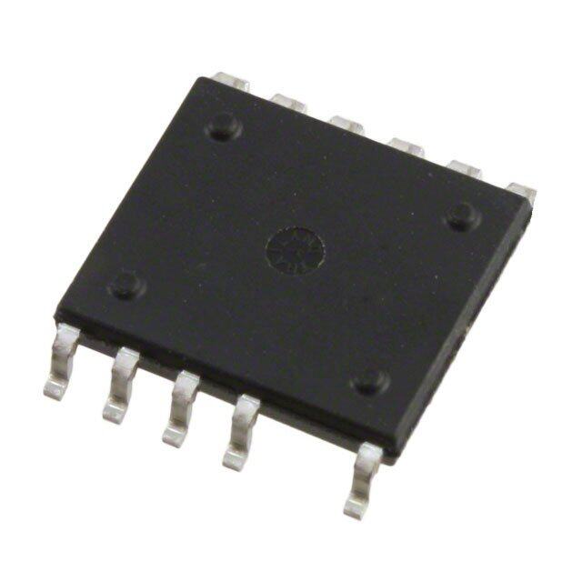
| 产品图片 |
|
| rohs | 符合RoHS无铅 / 符合限制有害物质指令(RoHS)规范要求 |
| 产品系列 | 电源管理 IC,开关控制器 ,Texas Instruments UCC3809PW-2- |
| 数据手册 | |
| 产品型号 | UCC3809PW-2 |
| PWM类型 | 电流模式 |
| 产品目录页面 | |
| 产品种类 | 开关控制器 |
| 倍增器 | 无 |
| 其它名称 | 296-12395-5 |
| 分频器 | 无 |
| 包装 | 管件 |
| 升压 | 是 |
| 占空比 | 70% |
| 占空比-最大 | 70 % |
| 反向 | 无 |
| 反激式 | 是 |
| 商标 | Texas Instruments |
| 安装风格 | SMD/SMT |
| 封装 | Tube |
| 封装/外壳 | 8-TSSOP(0.173",4.40mm 宽) |
| 封装/箱体 | TSSOP-8 |
| 工作温度 | 0°C ~ 70°C |
| 工厂包装数量 | 150 |
| 开关频率 | 1000 kHz |
| 拓扑结构 | Buck, Boost, Flyback, Forward |
| 最大工作温度 | + 70 C |
| 最小工作温度 | 0 C |
| 标准包装 | 150 |
| 电压-电源 | 8 V ~ 17.5 V |
| 类型 | Economy Primary Side PWM Controller |
| 系列 | UCC3809-2 |
| 输出数 | 1 |
| 输出端数量 | 1 Output |
| 配用 | /product-detail/zh/UCC3809EVM/296-12294-ND/416589 |
| 降压 | 是 |
| 隔离式 | 是 |
| 频率-最大值 | 1MHz |


- 商务部:美国ITC正式对集成电路等产品启动337调查
- 曝三星4nm工艺存在良率问题 高通将骁龙8 Gen1或转产台积电
- 太阳诱电将投资9.5亿元在常州建新厂生产MLCC 预计2023年完工
- 英特尔发布欧洲新工厂建设计划 深化IDM 2.0 战略
- 台积电先进制程称霸业界 有大客户加持明年业绩稳了
- 达到5530亿美元!SIA预计今年全球半导体销售额将创下新高
- 英特尔拟将自动驾驶子公司Mobileye上市 估值或超500亿美元
- 三星加码芯片和SET,合并消费电子和移动部门,撤换高东真等 CEO
- 三星电子宣布重大人事变动 还合并消费电子和移动部门
- 海关总署:前11个月进口集成电路产品价值2.52万亿元 增长14.8%


PDF Datasheet 数据手册内容提取
application UCC1809-1/-2 INFO UCC2809-1/-2 available UCC3809-1/-2 Economy Primary Side Controller FEATURES DESCRIPTION • UserProgrammableSoftStartWith The UCC3809 family of BCDMOS economy low power integrated circuits ActiveLowShutdown contains all the control and drive circuitry required for off-line and isolated DC-to-DC fixed frequency current mode switching power supplies with • UserProgrammableMaximumDuty minimal external parts count. Internally implemented circuits include Cycle undervoltage lockout featuring startup current less than 100µA, a user ac- • Accessible5VReference cessiblevoltagereference,logictoensurelatchedoperation,aPWMcom- parator, and a totem pole output stage to sink or source peak current. The • UndervoltageLockout output stage, suitable for driving N-Channel MOSFETs, is low in the off • Operationto1MHz state. • 0.4ASource/0.8ASinkFETDriver Oscillator frequency and maximum duty cycle are programmed with two resistors and a capacitor. The UCC3809 family also features full cycle soft • Low100µAStartupCurrent start. The family has UVLO thresholds and hysteresis levels for off-line and DC-to-DCsystemsasshowninthetabletotheleft. PART TURNON TURNOFF The UCC3809 and the UCC2809 are offered in the 8 pin SOIC (D), PDIP NUMBER THRESHOLD THRESHOLD (N), TSSOP (PW), and MSOP (P) packages. The small TSSOP and UCCX809-1 10V 8V MSOP packages make the device ideal for applications where board UCCX809-2 15V 8V spaceandheightareatapremium. TYPICAL APPLICATION DIAGRAM R START V IN FB 1V – 1 + 1V FNILOTISEER +5V +– R5EVF 8 REF FEEDBACK SS 6µA CREF 2 – CUSERNRSEENT SCLOOMPPE C 0.5V + VDD VOUT SS – 7 DISABLE + 15/8V 10/8V UVLO 17.5V C VDD RT1 PWM LATCH 3 R OUT CLK OSC Q 6 – RT2 S + 4 GND V C 5 REF T UDG-99036 SLUS166B-NOVEMBER1999-REVISEDNOVEMBER2004
UCC1809-1/-2 UCC2809-1/-2 UCC3809-1/-2 ABSOLUTE MAXIMUM RATINGS* CONNECTION DIAGRAM VDD...........................................19V SOIC-8,DIL-8 (TopView) I ..........................................25mA VDD IOUT(tpw<1µsandDutyCycle<10%)........–0.4Ato0.8A D,NandJPackages RT1,RT2,SS......................–0.3VtoREF+0.3V I .........................................–15mA REF StorageTemperature...................–65°Cto+150°C JunctionTemperature...................–55°Cto+150°C LeadTemperature(Soldering,10sec.).............+300°C *Valuesbeyondwhichdamagemayoccur. Allvoltagesarewithrespecttogroundunlessotherwisestated. Currents are positive into, negative out of the specified termi- nal. Consult Packaging Section of Databook for thermal limita- tionsandconsiderationsofpackages. TSSOP-8 (TopView) MSOP-8 (TopView) PWPackage PPackage 1 FB REF 8 1 FB REF 8 2 SS VDD 7 2 SS VDD 7 3 RT1 OUT 6 3 RT1 OUT 6 4 RT2 GND 5 4 RT2 GND 5 ORDERING INFORMATION TemperatureRange AvailablePackages UCC 809 – UCC1809-X –55°Cto+125°C J UVLOOPTION UCC2809-X –40°Cto+85°C N,D,P,PW PACKAGE UCC3809-X 0°Cto+70°C N,D,P,PW TEMPERATURERANGE ELECTRICAL CHARACTERISTICS:Unlessotherwisespecified,C =0.47(cid:1)F,VDD=12V.T =T . VREF A J PARAMETER TESTCONDITIONS MIN TYP MAX UNIT SupplySection VDDClamp I =10mA 16 17.5 19 V VDD IVDD NoLoad 600 900 µA IVDDStarting (Note1) 110 µA IVDD Standby UCCx809-1,VDD=StartThreshold-300mV 110 125 µA UCCx809-2,VDD=StartThreshold-300mV 130 170 µA UndervoltageLockoutSection StartThreshold(UCCx809-1) 9.4 10.4 V UVLOHysteresis(UCCx809-1) 1.65 V StartThreshold(UCCx809-2) 14.0 15.6 V UVLOHysteresis(UCCx809-2) 6.2 V VoltageReferenceSection OutputVoltage I =0mA 4.75 5 5.25 V REF LineRegulation VDD=10Vto15V 2 mV LoadRegulation I =0mAto5mA 2 mV REF ComparatorSection IFB OutputOff –100 nA ComparatorThreshold 0.9 0.95 1 V OUTPropagationDelay(NoLoad) V =0.8Vto1.2VatT =10ns 50 100 ns FB R 2
UCC1809-1/-2 UCC2809-1/-2 UCC3809-1/-2 ELECTRICAL CHARACTERISTICS:Unlessotherwisespecified,C =0.47(cid:1)F,VDD=12V.T =T . VREF A J PARAMETER TESTCONDITIONS MIN TYP MAX UNIT SoftStartSection ISS VDD=16V,VSS=0V;–40(cid:4)Cto(cid:5)85(cid:4)C –4.9 –7.0 –9.1 (cid:1)A VDD=16V,VSS=0V;(cid:6)–40(cid:4)C; (cid:7)(cid:5)85(cid:4)C –4.0 –7.0 –10.0 (cid:1)A VSSLow VDD=7.5V,ISS=200(cid:1)A 0.2 V ShutdownThreshold 0.44 0.48 0.52 V OscillatorSection Frequency RT1=10k,RT2=4.32k,CT=820pF 90 100 110 kHz FrequencyChangewithVoltage VDD=10Vto15V 0.1 %/V CTPeakVoltage 3.33 V CT ValleyVoltage 1.67 V CT PeaktoPeakVoltage 1.54 1.67 1.80 V OutputSection OutputVSATLow IOUT=80mA(dc) 0.8 1.5 V OutputVSAT High IOUT=–40mA(dc),VDD–OUT 0.8 1.5 V OutputLowVoltageDuringUVLO I =20mA(dc) 1.5 V OUT MinimumDutyCycle V =2V 0 % FB MaximumDutyCycle 70 % RiseTime C =1nF 35 ns OUT FallTime C =1nF 18 ns OUT Note1.Ensuredbydesign.Not100%productiontested. PIN DESCRIPTIONS FB: This pin is the summing node for current sense RT2: This pin connects to timing resistor RT2 and feedback, voltage sense feedback (by optocoupler) and controlsthenegativeramptimeoftheinternaloscillator slope compensation. Slope compensation is derived (Tf = 0.74 (cid:3) (CT + 27pF) (cid:3) RT2). The negative threshold from the rising voltage at the timing capacitor and can be of the internal oscillator is sensed through inactive timing buffered with an external small signal NPN transistor. resistor RT1 which connects to pin RT1 and timing External high frequency filter capacitance applied from capacitorCT. this node to GND is discharged by an internal 250(cid:2) on SS: This pin serves two functions. The soft start timing resistance NMOS FET during PWM off time and offers capacitor connects to SS and is charged by an internal effective leading edge blanking set by the RC time 6µA current source. Under normal soft start SS is constant of the feedback resistance from current sense dischargedtoatleast0.4Vandthenrampspositiveto1V resistortoFBinputandthehighfrequencyfiltercapacitor during which time the output driver is held low. As SS capacitanceatthisnodetoGND. charges from 1V to 2V soft start is implemented by an GND: Reference ground and power ground for all increasing output duty cycle. If SS is taken below 0.5V, functions. the output driver is inhibited and held low. The user OUT: This pin is the high current power driver output. A accessible 5V voltage reference also goes low and IVDD minimum series gate resistor of 3.9(cid:2) is recommended to <100(cid:1)A. limit the gate drive current when operating with high bias VDD: The power input connection for this device. This voltages. pinisshuntregulatedat17.5Vwhichissufficientlybelow the voltage rating of the DMOS output driver stage. VDD REF:The internal 5V reference output. This reference is shouldbebypassedwitha1(cid:1)Fceramiccapacitor. buffered and is available on the REF pin. REF should be bypassedwitha0.47(cid:1)Fceramiccapacitor. RT1: This pin connects to timing resistor RT1 and controls the positive ramp time of the internal oscillator (Tr=0.74(cid:3)(CT+27pF)(cid:3)RT1).Thepositivethresholdof the internal oscillator is sensed through inactive timing resistor RT2 which connects to pin RT2 and timing capacitorCT. 3
UCC1809-1/-2 UCC2809-1/-2 UCC3809-1/-2 APPLICATION INFORMATION UT UT VO VO + C19330Fµ6.3V – C18330Fµ6.3V R1712.1K1% R1612.1K1% C17330Fµ6.3V C130.1FµC14470pFR1510K LC16330Fµ6.3V T C R14750 U4TL431 U2BR2535 M 3 2 1 R195.1K3W C150.015Fµ 1 2 H11AV1 U3 T180Hµ 5:1 Q3RF640 R80.153W 5 4 C100.22Fµ D3SF24 I R715K R9R132K1.1K3W Q22N2907A R11680 R1010 R61K D21N5245 D41N5240 R1227K C70.47Fµ C90.1Fµ D15231B C81Fµ F C6330p UCC3809 FBREF8 SVSDD7 RT1OUT6 RT2GND5 U1 R205.62K C22Q420.1FN2222Aµ R183.01K 1 2 3 4 K R5470 R46.19 K C51nF C31Fµ PGND1 TP1 R312.1 C40.01Fµ A Q1N2222 2 C2150Fµ R15.1k R21.1K GND1 P C1150Fµ OFF VIN ON/ VIN UDG-99179 + – Figure1.Isolated50WflybackconverterutilizingtheUCC3809. Theswitchingfrequencyis70kHz,Vin=-32Vto -72V,Vout=+5V,Iout=0Ato10A 4
UCC1809-1/-2 UCC2809-1/-2 UCC3809-1/-2 APPLICATION INFORMATION (cont.) The Typical Application Diagram shows an isolated reference)sensedthroughRT1. TheRinputtotheoscil- flyback converter utilizing the UCC3809. Note that the lator latch, R(OSC), is also level sensitive and resets the capacitors C and C are local decoupling capaci- CLK signal low when CT crosses the 1.67V threshold, REF VDD tors for the reference and IC input voltage, respectively. turningoffQ2andturningonQ1,initiatinganothercharg- Both capacitors should be low ESR and ESL ceramic, ingcycle. placed as close to the IC pins as possible, and returned Figure 3 shows the waveforms associated with the oscil- directly to the ground pin of the chip for best stability. lator latch and the PWM latch (shown in the Typical Ap- REF provides the internal bias to many of the IC func- plication Diagram). Ahigh CLK signal not only initiates a tionsandCREFshouldbeatleast0.47µFtopreventREF dischargecycleforCT,italsoturnsontheinternalNMOS fromdrooping. FET on the FB pin causing any external capacitance FBPin used for leading edge blanking connected to this pin to be discharged to ground. By discharging any external The basic premise of the UCC3809 is that the voltage capacitor completely to ground during the external sense feedback signal originates from an optocoupler switch’s off-time, the noise immunity of the converter is that is modulated by an external error amplifier located enhancedallowingtheusertodesigninsmallerRCcom- on the secondary side. This signal is summed with the ponents for leading edge blanking. A high CLK signal current sense signal and any slope compensation at the also sets the level sensitive S input of the PWM latch, FB pin and compared to a 1V threshold, as shown in the S(PWM), high, resulting in a high output, Q(PWM), as Typical Application Diagram. Crossing this 1V threshold shown in Figure 3. This Q(PWM) signal will remain high resets the PWM latch and modulates the output driver untilaresetsignal,R(PWM)isreceived. AhighR(PWM) on-time much like the current sense comparator used in signal results from the FB signal crossing the 1V thresh- the UC3842. In the absence of a FB signal, the output old,orduringsoftstartoriftheSSpinisdisabled. will follow the programmed maximum on-time of the os- cillator. Assuming the UVLO threshold is satisfied, the OUT sig- nal of the IC will be high as long as Q(PWM) is high and When adding slope compensation, it is important to use S(PWM), also referred to as CLK, is low. The OUT sig- a small capacitor to AC couple the oscillator waveform nal will be dominated by the FB signal as long as the FB before summing this signal into the FB pin. By correctly signal trips the 1V threshold while CLK is low. If the FB selecting the emitter resistor of the optocoupler, the volt- signal does not cross the 1V threshold while CLK is low, age sense signal can force the FB node to exceed the the OUT signal will be dominated by the maximum duty 1V threshold when the output that is being compared ex- cycle programmed by the user. Figure 3 illustrates the ceeds a desired level. Doing so drives the UCC3809 to various waveforms for a design set up for a maximum zeropercentdutycycle. dutycycleof70%. Oscillator Thefollowingequationsetstheoscillatorfrequency: FOSC =[0.74•(CT +27pF)•(RT1+RT2)]−1 VREF DMAX =0.74•RT1•(CT +27pF)•FOSC Q1 Referring to Figure 2 and the waveforms in Figure 3, when Q1is on, CT charges via the R of Q1 and 3 + DS(on) S Q CLK RT1. During this charging process, the voltage of CT is 3.33V – RT1 sensed through RT2. The S input of the oscillator latch, + 4 R S(OSC), is level sensitive, so crossing the upper thresh- 1.67V – old (set at 2/3 VREF or 3.33V for a typical 5.0V refer- RT2 Q2 OSCILLATOR LATCH ence) sets the Q output (CLK signal) of the oscillator latchhigh.AhighCLKsignalresultsinturningoffQ1and CT OSC turning on Q2. CT now discharges through RT2 and the R of Q2. CT discharges from 3.33V to the lower DS(on) UDG-97195 threshold (set at 1/3 VREF or 1.67V for a typical 5.0V Figure2. UCC3809oscillator. 5
UCC1809-1/-2 UCC2809-1/-2 UCC3809-1/-2 APPLICATION INFORMATION (cont.) CT CT CHARGING DISCHARGING 3.33V 1.67V CT S(OSC) R(OSC) Q(OSC)=CLK =S(PWM) 1V FB R(PWM) Q(PWM) 70% 30% ON OFF OUT FBSIGNALDOMINANT MAX.DUTYCYCLEDOMINANT UDG-99037 Figure3.WaveformsassociatedwiththeoscillatorlatchandthePWMlatch. The recommended value for CTis 1nF for frequencies in 1000 the 100 kHz or less range and smaller CT for higher fre- quencies. The minimum recommended values of RT1 andRT2are10kΩand4.32kΩ,respectively.Usingthese values maintains a ratio of at least 20:1 between the z] H RDS(on)oftheinternalFETsandtheexternaltimingresis- [k tors, resulting in minimal change in frequency over tem- CY N 100 perature. Because of the oscillator's susceptibility to E U capacitive coupling, examine the oscillator frequency by Q E looking at the common RT1-RT2-CT node on the circuit R F board as opposed to looking at pins 3 and 4 directly. For good noise immunity, RT1 and RT2 should be placed as close to pins 3 and 4 of the IC as possible. CTshould be returned directly to the ground pin of the IC with minimal 10 strayinductanceandcapacitance. 100 1000 10000 CT[pF] Figure4.Oscillatorfrequencyvs.C (RT1=10k, T RT2=4.32k) 6
UCC1809-1/-2 UCC2809-1/-2 UCC3809-1/-2 APPLICATION INFORMATION (cont.) Synchronization changed. Both of the synchronization schemes shown in Figure 5 Option II uses the synchronization pulse to superimpose canbesuccessfullyimplementedwiththeinternaloscilla- the sync voltage onto the peak of the CT waveform. This tor of the UCC3809. Both schemes allow access to the triggers the internal 3.33V comparator, initiating a dis- timing ramp needed for slope compensation and have charge cycle. The sync pulse is summed with the free minimalimpactontheprogrammedmaximumdutycycle. runningoscillatorwaveformattheCTnode,resultingina In the absence of a sync pulse, the PWM controller will spikeontopoftheCTpeakvoltage. runindependentlyatthefrequencysetbyRT1,RT2,and ADDITIONALINFORMATION CT. This free running frequency must be approximately 15 to 20% lower than the sync pulse frequency to insure Please refer to the following Unitrode application topics the free running oscillator does not cross the comparator foradditionalinformation. thresholdbeforethedesiredsyncpulse. [1]ApplicationNoteU-165,DesignReview:Isolated50W Option I uses the synchronization pulse to pull pin 3 low, Flyback Converter with the UCC3809 Primary Side Con- triggering the internal 1.67V comparator to reset the RS trollerbyLisaDinwoodie. latch and initiate a charging cycle. The valley voltage of [2] Design Note DN-89, Comparing the UC3842, the CT waveform is higher when synchronized using this UCC3802, and UCC3809 Primary Side PWM Controllers configuration,decreasingtherampchargeanddischarge byLisaDinwoodie. times, thereby increasing the operating frequency; other- wise the overall shape of the CTvoltage waveform is un- 1k 3 +5V 3 UCC3809 UCC3809 SYNC 2N2222A OSCILLATOR OSCILLATOR RT1 4 RT1 4 PULSE SYNC 2N2222A RT2 PULSE RT2 424 CT CT 0.1µF 424 24 OPTIONI OPTIONII UDG-99006 Figure5. UCC3809synchronizationoptions. 7
UCC1809-1/-2 UCC2809-1/-2 UCC3809-1/-2 TYPICAL CHARACTERISTICS CURVES 16 180 160 UCC2809-2 14 140 UCC2809-1 12 A) 120 10 dby(u 100 O(V) 8 an 80 VL st U 6 d 60 d I 2809-2UVLOon 40 4 2809-1UVLOon 20 2 UVLOoff 0 0 -50 -25 0 25 50 75 100 125 -50 -25 0 25 50 75 100 125 Temperature(degC) Temperature(degC) Figure6.I (standby)vs.temperature. Figure7.UVLOvs.temperature. DD 110 Hz) 105 k ( y c n e u q 100 e fr or at cill 95 s O 90 -50 -25 0 25 50 75 100 125 temperature(degC) Figure8.Oscillatorfrequencyvs.temperature. REVISION HISTORY REV.B11/04 AddedIvddStand-byCurrentspecificationsintheElectricalCharacteristicstable. ModifiedIvddStartingspecificationsintheElectricalCharacteristicstable. AddedTypicalCharacteristicsCurvesforIdd(Standby),UVLOthresholds,andOscillatorFrequency. 8
PACKAGE OPTION ADDENDUM www.ti.com 6-Feb-2020 PACKAGING INFORMATION Orderable Device Status Package Type Package Pins Package Eco Plan Lead/Ball Finish MSL Peak Temp Op Temp (°C) Device Marking Samples (1) Drawing Qty (2) (6) (3) (4/5) UCC2809D-1 ACTIVE SOIC D 8 75 Green (RoHS NIPDAU Level-1-260C-UNLIM -40 to 85 2809-1 & no Sb/Br) D-1 UCC2809D-2 ACTIVE SOIC D 8 75 Green (RoHS NIPDAU Level-1-260C-UNLIM -40 to 85 2809-2 & no Sb/Br) D-2 UCC2809DTR-1 ACTIVE SOIC D 8 2500 Green (RoHS NIPDAU Level-1-260C-UNLIM -40 to 85 2809-1 & no Sb/Br) D-1 UCC2809DTR-1G4 ACTIVE SOIC D 8 2500 Green (RoHS NIPDAU Level-1-260C-UNLIM -40 to 85 2809-1 & no Sb/Br) D-1 UCC2809DTR-2 ACTIVE SOIC D 8 2500 Green (RoHS NIPDAU Level-1-260C-UNLIM -40 to 85 2809-2 & no Sb/Br) D-2 UCC2809P-1 ACTIVE VSSOP DGK 8 80 Green (RoHS NIPDAUAG Level-2-260C-1 YEAR -40 to 85 28091 & no Sb/Br) UCC2809P-2 ACTIVE VSSOP DGK 8 80 Green (RoHS NIPDAUAG Level-2-260C-1 YEAR -40 to 85 28092 & no Sb/Br) UCC2809PTR-1 ACTIVE VSSOP DGK 8 2500 Green (RoHS NIPDAUAG Level-2-260C-1 YEAR -40 to 85 28091 & no Sb/Br) UCC2809PTR-1G4 ACTIVE VSSOP DGK 8 2500 Green (RoHS NIPDAUAG Level-2-260C-1 YEAR -40 to 85 28091 & no Sb/Br) UCC2809PTR-2 ACTIVE VSSOP DGK 8 2500 Green (RoHS NIPDAUAG Level-2-260C-1 YEAR -40 to 85 28092 & no Sb/Br) UCC2809PW-1 ACTIVE TSSOP PW 8 150 Green (RoHS NIPDAU Level-2-260C-1 YEAR -40 to 85 28091 & no Sb/Br) UCC2809PW-2 ACTIVE TSSOP PW 8 150 Green (RoHS NIPDAU Level-2-260C-1 YEAR -40 to 85 28092 & no Sb/Br) UCC2809PWTR-1 ACTIVE TSSOP PW 8 2000 Green (RoHS NIPDAU Level-2-260C-1 YEAR -40 to 85 28091 & no Sb/Br) UCC2809PWTR-1G4 ACTIVE TSSOP PW 8 2000 Green (RoHS NIPDAU Level-2-260C-1 YEAR -40 to 85 28091 & no Sb/Br) UCC3809D-1 ACTIVE SOIC D 8 75 Green (RoHS NIPDAU Level-1-260C-UNLIM 0 to 70 3809-1 & no Sb/Br) D-1 UCC3809D-2 ACTIVE SOIC D 8 75 Green (RoHS NIPDAU Level-1-260C-UNLIM 0 to 70 3809-2 & no Sb/Br) D-2 UCC3809DTR-1 ACTIVE SOIC D 8 2500 Green (RoHS NIPDAU Level-1-260C-UNLIM 0 to 70 (3809-1, UCC3809) & no Sb/Br) D-1 Addendum-Page 1
PACKAGE OPTION ADDENDUM www.ti.com 6-Feb-2020 Orderable Device Status Package Type Package Pins Package Eco Plan Lead/Ball Finish MSL Peak Temp Op Temp (°C) Device Marking Samples (1) Drawing Qty (2) (6) (3) (4/5) UCC3809DTR-1G4 ACTIVE SOIC D 8 2500 Green (RoHS NIPDAU Level-1-260C-UNLIM 0 to 70 (3809-1, UCC3809) & no Sb/Br) D-1 UCC3809DTR-2 ACTIVE SOIC D 8 2500 Green (RoHS NIPDAU Level-1-260C-UNLIM 0 to 70 3809-2 & no Sb/Br) D-2 UCC3809N-1 ACTIVE PDIP P 8 50 Green (RoHS NIPDAU N / A for Pkg Type 0 to 70 UCC3809N-1 & no Sb/Br) UCC3809N-2 ACTIVE PDIP P 8 50 Green (RoHS NIPDAU N / A for Pkg Type 0 to 70 UCC3809N-2 & no Sb/Br) UCC3809P-1 ACTIVE VSSOP DGK 8 80 Green (RoHS NIPDAUAG Level-2-260C-1 YEAR 0 to 70 38091 & no Sb/Br) UCC3809P-2 ACTIVE VSSOP DGK 8 80 Green (RoHS NIPDAUAG Level-2-260C-1 YEAR 0 to 70 38092 & no Sb/Br) UCC3809PTR-1 ACTIVE VSSOP DGK 8 2500 Green (RoHS NIPDAUAG Level-2-260C-1 YEAR 0 to 70 38091 & no Sb/Br) UCC3809PTR-2 ACTIVE VSSOP DGK 8 2500 Green (RoHS NIPDAUAG Level-2-260C-1 YEAR 38092 & no Sb/Br) UCC3809PTR-2G4 ACTIVE VSSOP DGK 8 2500 Green (RoHS NIPDAUAG Level-2-260C-1 YEAR 38092 & no Sb/Br) UCC3809PW-2 ACTIVE TSSOP PW 8 150 Green (RoHS NIPDAU Level-2-260C-1 YEAR 0 to 70 38092 & no Sb/Br) (1) The marketing status values are defined as follows: ACTIVE: Product device recommended for new designs. LIFEBUY: TI has announced that the device will be discontinued, and a lifetime-buy period is in effect. NRND: Not recommended for new designs. Device is in production to support existing customers, but TI does not recommend using this part in a new design. PREVIEW: Device has been announced but is not in production. Samples may or may not be available. OBSOLETE: TI has discontinued the production of the device. (2) RoHS: TI defines "RoHS" to mean semiconductor products that are compliant with the current EU RoHS requirements for all 10 RoHS substances, including the requirement that RoHS substance do not exceed 0.1% by weight in homogeneous materials. Where designed to be soldered at high temperatures, "RoHS" products are suitable for use in specified lead-free processes. TI may reference these types of products as "Pb-Free". RoHS Exempt: TI defines "RoHS Exempt" to mean products that contain lead but are compliant with EU RoHS pursuant to a specific EU RoHS exemption. Green: TI defines "Green" to mean the content of Chlorine (Cl) and Bromine (Br) based flame retardants meet JS709B low halogen requirements of <=1000ppm threshold. Antimony trioxide based flame retardants must also meet the <=1000ppm threshold requirement. (3) MSL, Peak Temp. - The Moisture Sensitivity Level rating according to the JEDEC industry standard classifications, and peak solder temperature. Addendum-Page 2
PACKAGE OPTION ADDENDUM www.ti.com 6-Feb-2020 (4) There may be additional marking, which relates to the logo, the lot trace code information, or the environmental category on the device. (5) Multiple Device Markings will be inside parentheses. Only one Device Marking contained in parentheses and separated by a "~" will appear on a device. If a line is indented then it is a continuation of the previous line and the two combined represent the entire Device Marking for that device. (6) Lead/Ball Finish - Orderable Devices may have multiple material finish options. Finish options are separated by a vertical ruled line. Lead/Ball Finish values may wrap to two lines if the finish value exceeds the maximum column width. Important Information and Disclaimer:The information provided on this page represents TI's knowledge and belief as of the date that it is provided. TI bases its knowledge and belief on information provided by third parties, and makes no representation or warranty as to the accuracy of such information. Efforts are underway to better integrate information from third parties. TI has taken and continues to take reasonable steps to provide representative and accurate information but may not have conducted destructive testing or chemical analysis on incoming materials and chemicals. TI and TI suppliers consider certain information to be proprietary, and thus CAS numbers and other limited information may not be available for release. In no event shall TI's liability arising out of such information exceed the total purchase price of the TI part(s) at issue in this document sold by TI to Customer on an annual basis. Addendum-Page 3
PACKAGE MATERIALS INFORMATION www.ti.com 17-Jul-2020 TAPE AND REEL INFORMATION *Alldimensionsarenominal Device Package Package Pins SPQ Reel Reel A0 B0 K0 P1 W Pin1 Type Drawing Diameter Width (mm) (mm) (mm) (mm) (mm) Quadrant (mm) W1(mm) UCC2809DTR-1 SOIC D 8 2500 330.0 12.4 6.4 5.2 2.1 8.0 12.0 Q1 UCC2809DTR-2 SOIC D 8 2500 330.0 12.4 6.4 5.2 2.1 8.0 12.0 Q1 UCC2809PTR-1 VSSOP DGK 8 2500 330.0 12.4 5.3 3.4 1.4 8.0 12.0 Q1 UCC2809PTR-2 VSSOP DGK 8 2500 330.0 12.4 5.3 3.4 1.4 8.0 12.0 Q1 UCC2809PWTR-1 TSSOP PW 8 2000 330.0 12.4 7.0 3.6 1.6 8.0 12.0 Q1 UCC3809DTR-1 SOIC D 8 2500 330.0 12.4 6.4 5.2 2.1 8.0 12.0 Q1 UCC3809DTR-2 SOIC D 8 2500 330.0 12.4 6.4 5.2 2.1 8.0 12.0 Q1 UCC3809PTR-1 VSSOP DGK 8 2500 330.0 12.4 5.3 3.4 1.4 8.0 12.0 Q1 UCC3809PTR-2 VSSOP DGK 8 2500 330.0 12.4 5.3 3.4 1.4 8.0 12.0 Q1 PackMaterials-Page1
PACKAGE MATERIALS INFORMATION www.ti.com 17-Jul-2020 *Alldimensionsarenominal Device PackageType PackageDrawing Pins SPQ Length(mm) Width(mm) Height(mm) UCC2809DTR-1 SOIC D 8 2500 340.5 338.1 20.6 UCC2809DTR-2 SOIC D 8 2500 340.5 338.1 20.6 UCC2809PTR-1 VSSOP DGK 8 2500 366.0 364.0 50.0 UCC2809PTR-2 VSSOP DGK 8 2500 366.0 364.0 50.0 UCC2809PWTR-1 TSSOP PW 8 2000 367.0 367.0 35.0 UCC3809DTR-1 SOIC D 8 2500 340.5 338.1 20.6 UCC3809DTR-2 SOIC D 8 2500 340.5 338.1 20.6 UCC3809PTR-1 VSSOP DGK 8 2500 366.0 364.0 50.0 UCC3809PTR-2 VSSOP DGK 8 2500 366.0 364.0 50.0 PackMaterials-Page2
PACKAGE OUTLINE D0008A SOIC - 1.75 mm max height SCALE 2.800 SMALL OUTLINE INTEGRATED CIRCUIT C SEATING PLANE .228-.244 TYP [5.80-6.19] .004 [0.1] C A PIN 1 ID AREA 6X .050 [1.27] 8 1 2X .189-.197 [4.81-5.00] .150 NOTE 3 [3.81] 4X (0 -15 ) 4 5 8X .012-.020 B .150-.157 [0.31-0.51] .069 MAX [3.81-3.98] .010 [0.25] C A B [1.75] NOTE 4 .005-.010 TYP [0.13-0.25] 4X (0 -15 ) SEE DETAIL A .010 [0.25] .004-.010 0 - 8 [0.11-0.25] .016-.050 [0.41-1.27] DETAIL A (.041) TYPICAL [1.04] 4214825/C 02/2019 NOTES: 1. Linear dimensions are in inches [millimeters]. Dimensions in parenthesis are for reference only. Controlling dimensions are in inches. Dimensioning and tolerancing per ASME Y14.5M. 2. This drawing is subject to change without notice. 3. This dimension does not include mold flash, protrusions, or gate burrs. Mold flash, protrusions, or gate burrs shall not exceed .006 [0.15] per side. 4. This dimension does not include interlead flash. 5. Reference JEDEC registration MS-012, variation AA. www.ti.com
EXAMPLE BOARD LAYOUT D0008A SOIC - 1.75 mm max height SMALL OUTLINE INTEGRATED CIRCUIT 8X (.061 ) [1.55] SYMM SEE DETAILS 1 8 8X (.024) [0.6] SYMM (R.002 ) TYP [0.05] 5 4 6X (.050 ) [1.27] (.213) [5.4] LAND PATTERN EXAMPLE EXPOSED METAL SHOWN SCALE:8X SOLDER MASK SOLDER MASK METAL OPENING OPENING METAL UNDER SOLDER MASK EXPOSED METAL EXPOSED METAL .0028 MAX .0028 MIN [0.07] [0.07] ALL AROUND ALL AROUND NON SOLDER MASK SOLDER MASK DEFINED DEFINED SOLDER MASK DETAILS 4214825/C 02/2019 NOTES: (continued) 6. Publication IPC-7351 may have alternate designs. 7. Solder mask tolerances between and around signal pads can vary based on board fabrication site. www.ti.com
EXAMPLE STENCIL DESIGN D0008A SOIC - 1.75 mm max height SMALL OUTLINE INTEGRATED CIRCUIT 8X (.061 ) [1.55] SYMM 1 8 8X (.024) [0.6] SYMM (R.002 ) TYP [0.05] 5 4 6X (.050 ) [1.27] (.213) [5.4] SOLDER PASTE EXAMPLE BASED ON .005 INCH [0.125 MM] THICK STENCIL SCALE:8X 4214825/C 02/2019 NOTES: (continued) 8. Laser cutting apertures with trapezoidal walls and rounded corners may offer better paste release. IPC-7525 may have alternate design recommendations. 9. Board assembly site may have different recommendations for stencil design. www.ti.com
None
None
None
PACKAGE OUTLINE PW0008A TSSOP - 1.2 mm max height SCALE 2.800 SMALL OUTLINE PACKAGE C 6.6 TYP SEATING PLANE 6.2 PIN 1 ID A 0.1 C AREA 6X 0.65 8 1 3.1 2X 2.9 NOTE 3 1.95 4 5 0.30 8X 0.19 4.5 1.2 MAX B 0.1 C A B 4.3 NOTE 4 (0.15) TYP SEE DETAIL A 0.25 GAGE PLANE 0.15 0.75 0 - 8 0.05 0.50 DETAIL A TYPICAL 4221848/A 02/2015 NOTES: 1. All linear dimensions are in millimeters. Any dimensions in parenthesis are for reference only. Dimensioning and tolerancing per ASME Y14.5M. 2. This drawing is subject to change without notice. 3. This dimension does not include mold flash, protrusions, or gate burrs. Mold flash, protrusions, or gate burrs shall not exceed 0.15 mm per side. 4. This dimension does not include interlead flash. Interlead flash shall not exceed 0.25 mm per side. 5. Reference JEDEC registration MO-153, variation AA. www.ti.com
EXAMPLE BOARD LAYOUT PW0008A TSSOP - 1.2 mm max height SMALL OUTLINE PACKAGE 8X (1.5) 8X (0.45) SYMM (R0.05) 1 TYP 8 SYMM 6X (0.65) 5 4 (5.8) LAND PATTERN EXAMPLE SCALE:10X SOOPLEDNEINRG MASK METAL MSOELTDAEL RU NMDAESRK SOOPLEDNEINRG MASK 0.05 MAX 0.05 MIN ALL AROUND ALL AROUND NON SOLDER MASK SOLDER MASK DEFINED DEFINED SOLDER MASK DETAILS NOT TO SCALE 4221848/A 02/2015 NOTES: (continued) 6. Publication IPC-7351 may have alternate designs. 7. Solder mask tolerances between and around signal pads can vary based on board fabrication site. www.ti.com
EXAMPLE STENCIL DESIGN PW0008A TSSOP - 1.2 mm max height SMALL OUTLINE PACKAGE 8X (1.5) SYMM (R0.05) TYP 8X (0.45) 1 8 SYMM 6X (0.65) 5 4 (5.8) SOLDER PASTE EXAMPLE BASED ON 0.125 mm THICK STENCIL SCALE:10X 4221848/A 02/2015 NOTES: (continued) 8. Laser cutting apertures with trapezoidal walls and rounded corners may offer better paste release. IPC-7525 may have alternate design recommendations. 9. Board assembly site may have different recommendations for stencil design. www.ti.com
IMPORTANTNOTICEANDDISCLAIMER TI PROVIDES TECHNICAL AND RELIABILITY DATA (INCLUDING DATASHEETS), DESIGN RESOURCES (INCLUDING REFERENCE DESIGNS), APPLICATION OR OTHER DESIGN ADVICE, WEB TOOLS, SAFETY INFORMATION, AND OTHER RESOURCES “AS IS” AND WITH ALL FAULTS, AND DISCLAIMS ALL WARRANTIES, EXPRESS AND IMPLIED, INCLUDING WITHOUT LIMITATION ANY IMPLIED WARRANTIES OF MERCHANTABILITY, FITNESS FOR A PARTICULAR PURPOSE OR NON-INFRINGEMENT OF THIRD PARTY INTELLECTUAL PROPERTY RIGHTS. These resources are intended for skilled developers designing with TI products. You are solely responsible for (1) selecting the appropriate TI products for your application, (2) designing, validating and testing your application, and (3) ensuring your application meets applicable standards, and any other safety, security, or other requirements. These resources are subject to change without notice. TI grants you permission to use these resources only for development of an application that uses the TI products described in the resource. Other reproduction and display of these resources is prohibited. No license is granted to any other TI intellectual property right or to any third party intellectual property right. TI disclaims responsibility for, and you will fully indemnify TI and its representatives against, any claims, damages, costs, losses, and liabilities arising out of your use of these resources. TI’s products are provided subject to TI’s Terms of Sale (www.ti.com/legal/termsofsale.html) or other applicable terms available either on ti.com or provided in conjunction with such TI products. TI’s provision of these resources does not expand or otherwise alter TI’s applicable warranties or warranty disclaimers for TI products. Mailing Address: Texas Instruments, Post Office Box 655303, Dallas, Texas 75265 Copyright © 2020, Texas Instruments Incorporated