ICGOO在线商城 > 集成电路(IC) > PMIC - 栅极驱动器 > UCC27524ADGN
 Datasheet下载
- 型号: UCC27524ADGN
- 制造商: Texas Instruments
- 库位|库存: xxxx|xxxx
- 要求:
| 数量阶梯 | 香港交货 | 国内含税 |
| +xxxx | $xxxx | ¥xxxx |
查看当月历史价格
查看今年历史价格
UCC27524ADGN产品简介:
ICGOO电子元器件商城为您提供UCC27524ADGN由Texas Instruments设计生产,在icgoo商城现货销售,并且可以通过原厂、代理商等渠道进行代购。 UCC27524ADGN价格参考。Texas InstrumentsUCC27524ADGN封装/规格:PMIC - 栅极驱动器, Low-Side Gate Driver IC Non-Inverting 8-MSOP-PowerPad。您可以下载UCC27524ADGN参考资料、Datasheet数据手册功能说明书,资料中有UCC27524ADGN 详细功能的应用电路图电压和使用方法及教程。
UCC27524ADGN是Texas Instruments(德州仪器)生产的PMIC(电源管理集成电路)中的栅极驱动器型号,适用于多种电力电子应用场景。它具有高性能、低延迟和高电流输出等特点,广泛应用于需要高效驱动MOSFET或IGBT的场合。

1. 电机驱动:在电机控制系统中,UCC27524ADGN可以用于驱动逆变器中的功率开关器件(如MOSFET或IGBT),实现高效的电机控制。它能够快速响应PWM信号,确保电机运行的稳定性和效率。

2. 太阳能逆变器:在光伏系统中,UCC27524ADGN可以用于驱动DC-AC逆变器中的功率开关,帮助将直流电转换为交流电。其高驱动能力和快速开关特性有助于提高逆变器的效率和可靠性。

3. 不间断电源(UPS):在UPS系统中,UCC27524ADGN可以用于驱动逆变器电路中的功率开关,确保在市电中断时能够迅速切换到电池供电模式,并提供稳定的交流输出。

4. 工业自动化:在工业自动化设备中,UCC27524ADGN可用于驱动各种功率级电路,如伺服驱动器、PLC等。它能够提供强大的驱动电流,确保系统在高负载下的稳定运行。

5. 电动汽车(EV)和混合动力汽车(HEV):在电动汽车和混合动力汽车的动力系统中,UCC27524ADGN可以用于驱动车载逆变器和DC-DC转换器中的功率开关,支持车辆的高效能量转换和管理。

6. LED照明驱动:在大功率LED照明系统中,UCC27524ADGN可以用于驱动升压或降压转换器中的功率开关,确保LED灯的亮度和色温稳定,同时提高系统的能效。

总之,UCC27524ADGN凭借其优异的性能和广泛的适用性,在电力电子领域中扮演着重要角色,尤其适合需要高效驱动功率开关的应用场景。
| 参数 | 数值 |
| 产品目录 | 集成电路 (IC)半导体 |
| 描述 | IC GATE DVR LO-SIDE DL 8MSOP门驱动器 Dual Hi-Spd Low-Side Pwr MOSFET Dvr 5A |
| 产品分类 | PMIC - MOSFET,电桥驱动器 - 外部开关集成电路 - IC |
| 品牌 | Texas Instruments |
| 产品手册 | |
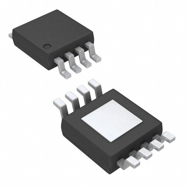
| 产品图片 |
|
| rohs | 符合RoHS无铅 / 符合限制有害物质指令(RoHS)规范要求 |
| 产品系列 | 电源管理 IC,门驱动器,Texas Instruments UCC27524ADGN- |
| 数据手册 | |
| 产品型号 | UCC27524ADGN |
| 上升时间 | 7 ns |
| 下降时间 | 7 ns |
| 产品 | MOSFET Gate Drivers |
| 产品种类 | 门驱动器 |
| 供应商器件封装 | 8-MSOP-PowerPad |
| 其它名称 | 296-36531-5 |
| 包装 | 管件 |
| 商标 | Texas Instruments |
| 安装类型 | 表面贴装 |
| 安装风格 | SMD/SMT |
| 封装 | Tube |
| 封装/外壳 | 8-TSSOP,8-MSOP(0.118",3.00mm 宽)裸焊盘 |
| 封装/箱体 | HVSSOP-8 |
| 工作温度 | -40°C ~ 140°C |
| 工厂包装数量 | 80 |
| 延迟时间 | - |
| 最大工作温度 | + 140 C |
| 最小工作温度 | - 40 C |
| 标准包装 | 80 |
| 激励器数量 | 2 Driver |
| 电压-电源 | 4.5 V ~ 18 V |
| 电流-峰值 | 5A |
| 电源电压-最大 | 18 V |
| 电源电压-最小 | 4.5 V |
| 电源电流 | 110 uA |
| 类型 | High Speed Low-Side Gate Driver |
| 系列 | UCC27524A |
| 输入类型 | 非反相 |
| 输出数 | 2 |
| 输出电流 | 5 A |
| 输出端数量 | 2 |
| 配置 | Dual, Non-Inverting |
| 配置数 | 2 |
| 高压侧电压-最大值(自举) | - |


- 商务部:美国ITC正式对集成电路等产品启动337调查
- 曝三星4nm工艺存在良率问题 高通将骁龙8 Gen1或转产台积电
- 太阳诱电将投资9.5亿元在常州建新厂生产MLCC 预计2023年完工
- 英特尔发布欧洲新工厂建设计划 深化IDM 2.0 战略
- 台积电先进制程称霸业界 有大客户加持明年业绩稳了
- 达到5530亿美元!SIA预计今年全球半导体销售额将创下新高
- 英特尔拟将自动驾驶子公司Mobileye上市 估值或超500亿美元
- 三星加码芯片和SET,合并消费电子和移动部门,撤换高东真等 CEO
- 三星电子宣布重大人事变动 还合并消费电子和移动部门
- 海关总署:前11个月进口集成电路产品价值2.52万亿元 增长14.8%


PDF Datasheet 数据手册内容提取
Product Sample & Technical Tools & Support & Folder Buy Documents Software Community UCC27524A SLUSBP4B–AUGUST2013–REVISEDOCTOBER2014 UCC27524A Dual 5-A, High-Speed, Low-Side Gate Driver With Negative Input Voltage Capability 1 Features 3 Description • Industry-StandardPinOut The UCC27524A device is a dual-channel, high- 1 speed, low-side, gate-driver device capable of • TwoIndependentGate-DriveChannels effectively driving MOSFET and IGBT power • 5-APeakSourceandSink-DriveCurrent switches. The UCC27524A is a variant of the • Independent-EnableFunctionforEachOutput UCC2752x family. The UCC27524A adds the ability to handle –5 V directly at the input pins for increased • TTLandCMOSCompatibleLogicThreshold robustness. The UCC27524A is a dual non-inverting IndependentofSupplyVoltage driver. Using a design that inherently minimizes • Hysteretic-LogicThresholdsforHighNoise shoot-through current, the UCC27524A is capable of Immunity delivering high-peak current pulses of up to 5-A • AbilitytoHandleNegativeVoltages(–5V)at source and 5-A sink into capacitive loads along with rail-to-rail drive capability and extremely small Inputs propagation delay typically 13 ns. In addition, the • InputsandEnablePin-VoltageLevelsNot drivers feature matched internal propagation delays RestrictedbyVDDPinBiasSupplyVoltage between the two channels which are very well suited • 4.5to18-VSingle-SupplyRange for applications requiring dual-gate drives with critical • OutputsHeldLowDuringVDD-UVLO(Ensures timing, such as synchronous rectifiers. This also enables connecting two channels in parallel to Glitch-FreeOperationatPowerUpandPower effectively increase current-drive capability or driving Down) two switches in parallel with a single input signal. The • FastPropagationDelays(13-nsTypical) input pin thresholds are based on TTL and CMOS • FastRiseandFallTimes(7-nsand6-nsTypical) compatible low-voltage logic, which is fixed and independent of the VDD supply voltage. Wide • 1-nsTypicalDelayMatchingBetween2-Channels hysteresisbetweenthehighandlowthresholdsoffers • TwoOutputsareParalleledforHigherDrive excellentnoiseimmunity. Current • OutputsHeldinLowWhenInputsFloating DeviceInformation(1) • SOIC-8,HVSSOP-8PowerPAD™Package PARTNUMBER PACKAGE BODYSIZE(NOM) Options SOIC(8) 4.90mmx3.91mm UCC27524A • OperatingTemperatureRangeof–40to140°C HVSSOP(8) 3.00mmx3.00mm (1) For all available packages, see the orderable addendum at 2 Applications theendofthedatasheet. • Switch-ModePowerSupplies DualNon-InvertingInputs • DC-to-DCConverters • MotorControl,SolarPower • GateDriveforEmergingWideBand-GapPower DevicesSuchasGaN 1 An IMPORTANT NOTICE at the end of this data sheet addresses availability, warranty, changes, use in safety-critical applications, intellectualpropertymattersandotherimportantdisclaimers.PRODUCTIONDATA.
UCC27524A SLUSBP4B–AUGUST2013–REVISEDOCTOBER2014 www.ti.com Table of Contents 1 Features.................................................................. 1 8.2 FunctionalBlockDiagram.......................................12 2 Applications........................................................... 1 8.3 FeatureDescription.................................................12 3 Description............................................................. 1 8.4 DeviceFunctionalModes........................................17 4 RevisionHistory..................................................... 2 9 ApplicationsandImplementation...................... 18 9.1 ApplicationInformation............................................18 5 Description(Continued)........................................ 3 9.2 TypicalApplication..................................................18 6 PinConfigurationandFunctions......................... 3 10 PowerSupplyRecommendations..................... 23 7 Specifications......................................................... 4 11 Layout................................................................... 23 7.1 AbsoluteMaximumRatings......................................4 11.1 LayoutGuidelines.................................................23 7.2 HandlingRatings.......................................................4 11.2 LayoutExample....................................................24 7.3 RecommendedOperatingConditions.......................4 11.3 ThermalProtection................................................24 7.4 ThermalInformation..................................................5 12 DeviceandDocumentationSupport................. 26 7.5 ElectricalCharacteristics...........................................6 7.6 SwitchingCharacteristics..........................................6 12.1 Trademarks...........................................................26 7.7 TypicalCharacteristics..............................................8 12.2 ElectrostaticDischargeCaution............................26 12.3 Glossary................................................................26 8 DetailedDescription............................................ 11 13 Mechanical,Packaging,andOrderable 8.1 Overview.................................................................11 Information........................................................... 26 4 Revision History ChangesfromRevisionA(August2013)toRevisionB Page • AddedPinConfigurationandFunctionssection,HandlingRatingtable,FeatureDescriptionsection,Device FunctionalModes,ApplicationandImplementationsection,PowerSupplyRecommendationssection,Layout section,DeviceandDocumentationSupportsection,andMechanical,Packaging,andOrderableInformation section ................................................................................................................................................................................... 1 ChangesfromOriginal(August2013)toRevisionA Page • ChangedmarketingstatusfromProductPreviewtoProductionData................................................................................... 1 • ChangedEnablevoltage,ENAandENBminimumfrom0to–2........................................................................................... 4 2 SubmitDocumentationFeedback Copyright©2013–2014,TexasInstrumentsIncorporated ProductFolderLinks:UCC27524A
UCC27524A www.ti.com SLUSBP4B–AUGUST2013–REVISEDOCTOBER2014 5 Description (Continued) For safety purpose, internal pull-up and pull-down resistors on the input pins of the UCC27524A ensure that outputs are held LOW when input pins are in floating condition. UCC27524A features Enable pins (ENA and ENB) to have better control of the operation of the driver applications. The pins are internally pulled up to VDD foractive-highlogicandareleftopenforstandardoperation. UCC27524AfamilyofdevicesareavailableinSOIC-8(D),VSSOP-8withexposedpad(DGN)packages. 6 Pin Configuration and Functions 8-Pin D,DGNPackage TopView ENA 1 8 ENB INA 2 7 OUTA GND 3 6 VDD INB 4 5 OUTB PinFunctions PIN I/O DESCRIPTION NAME NO. ENA 1 I EnableinputforChannelA:ENAisbiasedLOWtodisabletheChannelAoutputregardlessofthe INAstate.ENAisbiasedHIGHorleftfloatingtoenabletheChannelAoutput.ENAisallowedto float;hencethepin-to-pincompatibilitywiththeUCC2732XN/Cpin. ENB 8 I EnableinputforChannelB:ENBisbiasedLOWtodisablestheChannelBoutputregardlessofthe INBstate.ENBisbiasedHIGHorleftfloatingtoenableChannelBoutput.ENBisallowedtofloat hence;thepin-to-pincompatibilitywiththeUCC2752AN/Cpin. GND 3 - Ground:Allsignalsarereferencedtothispin. INA 2 I InputtoChannelA:INAisthenon-invertinginputintheUCC27524Adevice.OUTAisheldLOWif INAisunbiasedorfloating. INB 4 I InputtoChannelB:INBisthenon-invertinginputintheUCC27524Adevice.OUTBisheldLOWif INBisunbiasedorfloating. OUTA 7 O OutputofChannelA OUTB 5 O OutputofChannelB VDD 6 I Biassupplyinput Copyright©2013–2014,TexasInstrumentsIncorporated SubmitDocumentationFeedback 3 ProductFolderLinks:UCC27524A
UCC27524A SLUSBP4B–AUGUST2013–REVISEDOCTOBER2014 www.ti.com 7 Specifications 7.1 Absolute Maximum Ratings(1)(2) overoperatingfree-airtemperaturerange(unlessotherwisenoted) MIN MAX UNIT Supplyvoltagerange VDD –0.3 20 V DC –0.3 VDD+0.3 V OUTA,OUTBvoltage Repetitivepulse<200ns(3) –2 VDD+0.3 V Outputcontinuoussource/sinkcurrent I 0.3 A OUT_DC Outputpulsedsource/sinkcurrent(0.5µs) I 5 A OUT_pulsed INA,INB,ENA,ENBvoltage(4) –5 20 V Operatingvirtualjunctiontemperature,T range –40 150 °C J Soldering,10seconds 300 °C Leadtemperature Reflow 260 °C (1) StressesbeyondthoselistedunderAbsoluteMaximumRatingsmaycausepermanentdamagetothedevice.Thesearestressratings onlyandfunctionaloperationofthedeviceattheseoranyotherconditionsbeyondthoseindicatedunderRecommendedOperating Conditionsisnotimplied.Exposuretoabsolute-maximum-ratedconditionsforextendedperiodsmayaffectdevicereliability. (2) AllvoltagesarewithrespecttoGNDunlessotherwisenoted.Currentsarepositiveinto,negativeoutofthespecifiedterminal.See PackagingSectionofthedatasheetforthermallimitationsandconsiderationsofpackages. (3) Valuesareverifiedbycharacterizationonbench. (4) ThemaximumvoltageontheInputandEnablepinsisnotrestrictedbythevoltageontheVDDpin. 7.2 Handling Ratings MIN MAX UNIT T Storagetemperaturerange –65 150 °C stg Humanbodymodel(HBM),perANSI/ESDA/JEDECJS-001,all pins(1) –4000 4000 V Electrostaticdischarge V (ESD) Chargeddevicemodel(CDM),perJEDECspecification JESD22-C101,allpins(2) –1000 1000 (1) JEDECdocumentJEP155statesthat500-VHBMallowssafemanufacturingwithastandardESDcontrolprocess. (2) JEDECdocumentJEP157statesthat250-VCDMallowssafemanufacturingwithastandardESDcontrolprocess. 7.3 Recommended Operating Conditions overoperatingfree-airtemperaturerange(unlessotherwisenoted) MIN TYP MAX UNIT Supplyvoltagerange,VDD 4.5 12 18 V Operatingjunctiontemperaturerange –40 140 °C Inputvoltage,INA,INB –2 18 V Enablevoltage,ENAandENB –2 18 4 SubmitDocumentationFeedback Copyright©2013–2014,TexasInstrumentsIncorporated ProductFolderLinks:UCC27524A
UCC27524A www.ti.com SLUSBP4B–AUGUST2013–REVISEDOCTOBER2014 7.4 Thermal Information UCC27524A UCC27524A THERMALMETRIC SOIC(D) MSOP(DGN)(1) UNIT 8PINS 8PINS θ Junction-to-ambientthermalresistance(2) 130.9 71.8 JA θ Junction-to-case(top)thermalresistance(3) 80.0 65.6 JCtop θ Junction-to-boardthermalresistance(4) 71.4 7.4 JB °C/W ψ Junction-to-topcharacterizationparameter(5) 21.9 7.4 JT ψ Junction-to-boardcharacterizationparameter(6) 70.9 31.5 JB θ Junction-to-case(bottom)thermalresistance(7) n/a 19.6 JCbot (1) Formoreinformationabouttraditionalandnewthermalmetrics,seetheICPackageThermalMetricsapplicationreport,SPRA953. (2) Thejunction-to-ambientthermalresistanceundernaturalconvectionisobtainedinasimulationonaJEDEC-standard,high-Kboard,as specifiedinJESD51-7,inanenvironmentdescribedinJESD51-2a. (3) Thejunction-to-case(top)thermalresistanceisobtainedbysimulatingacoldplatetestonthepackagetop.NospecificJEDEC- standardtestexists,butaclosedescriptioncanbefoundintheANSISEMIstandardG30-88. (4) Thejunction-to-boardthermalresistanceisobtainedbysimulatinginanenvironmentwitharingcoldplatefixturetocontrolthePCB temperature,asdescribedinJESD51-8. (5) Thejunction-to-topcharacterizationparameter,ψ ,estimatesthejunctiontemperatureofadeviceinarealsystemandisextracted JT fromthesimulationdataforobtainingθ ,usingaproceduredescribedinJESD51-2a(sections6and7). JA (6) Thejunction-to-boardcharacterizationparameter,ψ ,estimatesthejunctiontemperatureofadeviceinarealsystemandisextracted JB fromthesimulationdataforobtainingθ ,usingaproceduredescribedinJESD51-2a(sections6and7). JA (7) Thejunction-to-case(bottom)thermalresistanceisobtainedbysimulatingacoldplatetestontheexposed(power)pad.Nospecific JEDECstandardtestexists,butaclosedescriptioncanbefoundintheANSISEMIstandardG30-88. Spacer Copyright©2013–2014,TexasInstrumentsIncorporated SubmitDocumentationFeedback 5 ProductFolderLinks:UCC27524A
UCC27524A SLUSBP4B–AUGUST2013–REVISEDOCTOBER2014 www.ti.com 7.5 Electrical Characteristics V =12V,T =T =–40°Cto140°C,1-µFcapacitorfromV toGND.Currentsarepositiveinto,negativeoutofthe DD A J DD specifiedterminal(unlessotherwisenoted,) PARAMETER TESTCONDITION MIN TYP MAX UNIT BIASCURRENTS VDD=3.4V, INA=VDD, 55 110 175 Startupcurrent, INB=VDD I (basedonUCC27524Input μA DD(off) configuration) VDD=3.4V, INA=GND, 25 75 145 INB=GND UNDERVOLTAGELOCKOUT(UVLO) T =25°C 3.91 4.2 4.5 J V Supplystartthreshold ON T =–40°Cto140°C 3.7 4.2 4.65 J Minimumoperatingvoltage V V 3.4 3.9 4.4 OFF aftersupplystart VDD_H Supplyvoltagehysteresis 0.2 0.3 0.5 INPUTS(INA,INB,INA+,INA–,INB+,INB–),UCC27524A(D,DGN) Outputhighfornon-invertinginputpins V Inputsignalhighthreshold 1.9 2.1 2.3 IN_H Outputlowforinvertinginputpins Outputlowfornon-invertinginputpins V V Inputsignallowthreshold 1 1.2 1.4 IN_L Outputhighforinvertinginputpins V Inputhysteresis 0.7 0.9 1.1 IN_HYS OUTPUTS(OUTA,OUTB) I Sink/sourcepeakcurrent(1) C =0.22µF,F =1kHz ±5 A SNK/SRC LOAD SW V -V Highoutputvoltage I =–10mA 0.075 DD OH OUT V V Lowoutputvoltage I =10mA 0.01 OL OUT R Outputpullupresistance(2) I =–10mA 2.5 5 7.5 Ω OH OUT R Outputpulldownresistance I =10mA 0.15 0.5 1 Ω OL OUT (1) Ensuredbydesign. (2) R representson-resistanceofonlytheP-ChannelMOSFETdeviceinthepullupstructureoftheUCC27524Aoutputstage. OH 7.6 Switching Characteristics overoperatingfree-airtemperaturerange(unlessotherwisenoted) PARAMETER TESTCONDITIONS MIN TYP MAX UNIT t Risetime(1) C =1.8nF 7 18 R LOAD t Falltime(1) C =1.8nF 6 10 F LOAD INA=INB,OUTAandOUTBat50% t Delaymatchingbetween2channels 1 4 M transitionpoint ns Minimuminputpulsewidththat t 15 25 PW changestheoutputstate t ,t Inputtooutputpropagationdelay(1) C =1.8nF,5-Vinputpulse 6 13 23 D1 D2 LOAD t ,t ENtooutputpropagationdelay(1) C =1.8nF,5-Venablepulse 6 13 23 D3 D4 LOAD (1) SeethetimingdiagramsinFigure1andFigure2 6 SubmitDocumentationFeedback Copyright©2013–2014,TexasInstrumentsIncorporated ProductFolderLinks:UCC27524A
UCC27524A www.ti.com SLUSBP4B–AUGUST2013–REVISEDOCTOBER2014 High Input Low High Enable Low 90% Output 10% tD3 tD4 UDG-11217 Figure1. EnableFunction (ForNon-InvertingInput-DriverOperation) High Input Low High Enable Low 90% Output 10% tD1 tD2 UDG-11219 Figure2. Non-InvertingInput-DriverOperation Copyright©2013–2014,TexasInstrumentsIncorporated SubmitDocumentationFeedback 7 ProductFolderLinks:UCC27524A
UCC27524A SLUSBP4B–AUGUST2013–REVISEDOCTOBER2014 www.ti.com 7.7 Typical Characteristics 4 Input=VDD 0.14 Input=GND A) m A) nt ( nt (m 0.12 Curre 3.5 urre ply artup C 0.1 ng Sup 3 St ati VDD = 12 V 0.08 per fSW = 500 kHz O CL = 500 pF VDD=3.4V 0.06 2.5 −50 0 50 100 150 −50 0 50 100 150 Temperature (°C) Temperature (°C) G001 G002 Figure3.Start-UpCurrentvsTemperature Figure4.OperatingSupplyCurrentvsTemperature (OutputsSwitching) 0.6 5 Input=GND UVLO Rising Input=VDD UVLO Falling A) 0.5 V) 4.5 upply Current (m 0.4 VLO Threshold ( 4 S 0.3 U 3.5 Enable=12 V VDD = 12 V 0.2 3 −50 0 50 100 150 −50 0 50 100 150 Temperature (°C) Temperature (°C) G012 G003 Figure5.SupplyCurrentvsTemperature(OutputsInDC Figure6.UVLOThresholdvsTemperature On/OffCondition) 2.5 2.5 hold (V) 2 VDD = 12 V shold (V) 2 VDD = 12 V hres 1.5 Thre 1.5 ut T ble p a n n I 1 E 1 Input High Threshold Enable High Threshold Input Low Threshold Enable Low Threshold 0.5 0.5 −50 0 50 100 150 −50 0 50 100 150 Temperature (°C) Temperature (°C) G004 G005 Figure7.InputThresholdvsTemperature Figure8.EnableThresholdvsTemperature 8 SubmitDocumentationFeedback Copyright©2013–2014,TexasInstrumentsIncorporated ProductFolderLinks:UCC27524A
UCC27524A www.ti.com SLUSBP4B–AUGUST2013–REVISEDOCTOBER2014 Typical Characteristics (continued) 7 1 VDD = 12 V VDD = 12 V Wnce () 6 IOUT = −10 mA Wance () 0.8 IOUT = 10 mA esista Resist p R 5 wn 0.6 u o − d Pull ull− put 4 ut P 0.4 Out utp O 3 0.2 −50 0 50 100 150 −50 0 50 100 150 Temperature (°C) Temperature (°C) G006 G007 Figure9.OutputPullupResistancevsTemperature Figure10.OutputPulldownResistancevsTemperature 10 9 VDD = 12 V VDD = 12 V CLOAD = 1.8 nF CLOAD = 1.8 nF 9 8 me (ns) 8 me (ns) 7 Rise Ti 7 Fall Ti 6 6 5 5 −50 0 50 100 150 −50 0 50 100 150 Temperature (°C) Temperature (°C) G008 G009 Figure11.RiseTimevsTemperature Figure12.FallTimevsTemperature 18 18 nput to Output Propagation Delay (ns) 11110246 TTuurrnn−−oonff VCDLOD A=D 1=2 1 V.8 nF EN to Output Propagation Delay (ns) 11110246 EENN ttoo OOuuttppuutt HLoigwh VCDLOD A=D 1=2 1 V.8 nF I 8 8 −50 0 50 100 150 −50 0 50 100 150 Temperature (°C) Temperature (°C) G010 G011 Figure13.InputtoOutputPropagationDelayvs Figure14.EntoOutputPropagationDelayvsTemperature Temperature Copyright©2013–2014,TexasInstrumentsIncorporated SubmitDocumentationFeedback 9 ProductFolderLinks:UCC27524A
UCC27524A SLUSBP4B–AUGUST2013–REVISEDOCTOBER2014 www.ti.com Typical Characteristics (continued) 60 22 VDD = 4.5 V Input to Output On delay A) 50 VDD = 12 V Input to Ouptut Off Delay Current (m 40 CLOADV =D D1 .=8 1n5F V elays (ns) 18 EENN ttoo OOuuttppuutt OOnff DDeellaayy ply 30 Both channels switching n D 14 p o Su ati erating 20 Propag 10 p 10 O CLOAD = 1.8 nF 0 6 0 100 200 300 400 500 600 700 800 900 1000 4 8 12 16 20 Frequency (kHz) Supply Voltage (V) G013 G014 Figure15.OperatingSupplyCurrentvsFrequency Figure16.PropagationDelaysvsSupplyVoltage 18 10 CLOAD = 1.8 nF CLOAD = 1.8 nF me (ns) 14 me (ns) 8 Rise Ti 10 Fall Ti 6 6 4 4 8 12 16 20 4 8 12 16 20 Supply Voltage (V) Supply Voltage (V) G015 G016 Figure17.RiseTimevsSupplyVoltage Figure18.FallTimevsSupplyVoltage 2.5 Enable High Threshold VDD = 4.5 V Enable Low Threshold V) 2 d ( ol h s hre 1.5 T e bl a n E 1 0.5 −50 0 50 100 150 Temperature (°C) G017 Figure19.EnableThresholdvsTemperature 10 SubmitDocumentationFeedback Copyright©2013–2014,TexasInstrumentsIncorporated ProductFolderLinks:UCC27524A
UCC27524A www.ti.com SLUSBP4B–AUGUST2013–REVISEDOCTOBER2014 8 Detailed Description 8.1 Overview The UCC27524A device represents Texas Instruments’ latest generation of dual-channel low-side high-speed gate-driver devices featuring a 5-A source and sink current capability, industry best-in-class switching characteristics, and a host of other features listed in Table 1 all of which combine to ensure efficient, robust and reliableoperationinhigh-frequencyswitchingpowercircuits. Table1.UCC27524AFeaturesandBenefits FEATURE BENEFIT Best-in-class13-ns(typ)propagationdelay Extremelylow-pulsetransmissiondistortion Easeofparallelingoutputsforhigher(2times)currentcapability, 1-ns(typ)delaymatchingbetweenchannels easeofdrivingparallel-powerswitches ExpandedVDDOperatingrangeof4.5to18V Expandedoperatingtemperaturerangeof–40°Cto+140°C Flexibilityinsystemdesign (SeeElectricalCharacteristicstable) OutputsareheldLowinUVLOcondition,whichensurespredictable, VDDUVLOProtection glitch-freeoperationatpower-upandpower-down Safetyfeature,especiallyusefulinpassingabnormalconditiontests OutputsheldLowwheninputpins(INx)infloatingcondition duringsafetycertification Pin-to-pincompatibilitywiththeUCC27324devicefromTexas Outputsenablewhenenablepins(ENx)infloatingcondition Instruments,indesignswherePin1andPin8areinfloating condition Enhancednoiseimmunity,whileretainingcompatibilitywith CMOS/TTLcompatibleinputandenablethresholdwithwide microcontrollerlogic-levelinputsignals(3.3V,5V)optimizedfor hysteresis digitalpower Abilityofinputandenablepinstohandlevoltagelevelsnotrestricted Systemsimplification,especiallyrelatedtoauxiliarybiassupply byVDDpinbiasvoltage architecture Abilitytohandle–5V (max)atinputpins Increasedrobustnessinnoisyenvironments DC Copyright©2013–2014,TexasInstrumentsIncorporated SubmitDocumentationFeedback 11 ProductFolderLinks:UCC27524A
UCC27524A SLUSBP4B–AUGUST2013–REVISEDOCTOBER2014 www.ti.com 8.2 Functional Block Diagram V V DD DD 200kW 200kW ENA 1 8 ENB V DD INA OUTA 2 7 400kW VDD V DD VDD UVLO GND 3 6 V DD INB OUTB 4 5 400kW 8.3 Feature Description 8.3.1 OperatingSupplyCurrent The UCC27524A products feature very low quiescent I currents. The typical operating-supply current in UVLO DD state and fully-on state (under static and switching conditions) are summarized in Figure 3, Figure 4 and Figure 5. The I current when the device is fully on and outputs are in a static state (DC high or DC low, see DD Figure 4) represents lowest quiescent I current when all the internal logic circuits of the device are fully DD operational. The total supply current is the sum of the quiescent I current, the average I current because of DD OUT switching, and finally any current related to pullup resistors on the enable pins and inverting input pins. For examplewhentheinvertinginputpinsarepulledlowadditionalcurrentisdrawnfromtheVDDsupplythroughthe pullup resistors (see though ). Knowing the operating frequency (f ) and the MOSFET gate (Q ) charge at the SW G drivevoltagebeingused,theaverageI currentcanbecalculatedasproductofQ andf . OUT G SW A complete characterization of the I current as a function of switching frequency at different V bias voltages DD DD under 1.8-nF switching load in both channels is provided in Figure 15. The strikingly linear variation and close correlation with theoretical value of average I indicates negligible shoot-through inside the gate-driver device OUT attestingtoitshigh-speedcharacteristics. 8.3.2 InputStage The input pins of UCC27524A gate-driver devices are based on a TTL and CMOS compatible input-threshold logic that is independent of the VDD supply voltage. With typically high threshold = 2.1 V and typically low threshold = 1.2 V, the logic level thresholds are conveniently driven with PWM control signals derived from 3.3-V and 5-V digital power-controller devices. Wider hysteresis (typ 0.9 V) offers enhanced noise immunity compared to traditional TTL logic implementations, where the hysteresis is typically less than 0.5 V. UCC27524A devices also feature tight control of the input pin threshold voltage levels which eases system design considerations and ensures stable operation across temperature (refer to Figure 7). The very low input capacitance on these pins reducesloadingandincreasesswitchingspeed. 12 SubmitDocumentationFeedback Copyright©2013–2014,TexasInstrumentsIncorporated ProductFolderLinks:UCC27524A
UCC27524A www.ti.com SLUSBP4B–AUGUST2013–REVISEDOCTOBER2014 Feature Description (continued) The UCC27524A device features an important safety feature wherein, whenever any of the input pins is in a floating condition, the output of the respective channel is held in the low state. This is achieved using GND pulldownresistorsonallthenon-invertinginputpins(INA,INB),asshowninthedeviceblockdiagrams. The input stage of each driver is driven by a signal with a short rise or fall time. This condition is satisfied in typical power supply applications, where the input signals are provided by a PWM controller or logic gates with fast transition times (<200 ns) with a slow changing input voltage, the output of the driver may switch repeatedly at a high frequency. While the wide hysteresis offered in UCC27524A definitely alleviates this concern over most other TTL input threshold devices, extra care is necessary in these implementations. If limiting the rise or fall times to the power device is the primary goal, then an external resistance is highly recommended between the output of the driver and the power device. This external resistor has the additional benefit of reducing part of the gate-charge related power dissipation in the gate driver device package and transferring it into the external resistoritself. 8.3.3 EnableFunction The enable function is an extremely beneficial feature in gate-driver devices especially for certain applications such as synchronous rectification where the driver outputs disable in light-load conditions to prevent negative currentcirculationandtoimprovelight-loadefficiency. UCC27524A device is provided with independent enable pins ENx for exclusive control of each driver-channel operation. The enable pins are based on a non-inverting configuration (active-high operation). Thus when ENx pins are driven high the drivers are enabled and when ENx pins are driven low the drivers are disabled. Like the input pins, the enable pins are also based on a TTL and CMOS compatible input-threshold logic that is independent of the supply voltage and are effectively controlled using logic signals from 3.3-V and 5-V microcontrollers. The UCC27524A devices also feature tight control of the Enable-function threshold-voltage levels which eases system design considerations and ensures stable operation across temperature (refer to Figure 8). The ENx pins are internally pulled up to VDD using pullup resistors as a result of which the outputs of the device are enabled in the default state. Hence the ENx pins are left floating or Not Connected (N/C) for standard operation, where the enable feature is not needed. Essentially, this floating allows the UCC27524A device to be pin-to-pin compatible with TI’s previous generation of drivers (UCC27323, UCC27324, and UCC27325respectively),wherePin1andPin8areN/Cpins.IfthechannelAandChannelBinputsandoutputs are connected in parallel to increase the driver current capacity, ENA and ENB are connected and driven together. 8.3.4 OutputStage The UCC27524A device output stage features a unique architecture on the pullup structure which delivers the highest peak-source current when it is most needed during the Miller plateau region of the power-switch turnon transition (when the power switch drain or collector voltage experiences dV/dt). The output stage pullup structure features a P-Channel MOSFET and an additional N-Channel MOSFET in parallel. The function of the N-Channel MOSFET is to provide a brief boost in the peak sourcing current enabling fast turnon. This is accomplished by briefly turning-on the N-Channel MOSFET during a narrow instant when the output is changing state from Low to High. Copyright©2013–2014,TexasInstrumentsIncorporated SubmitDocumentationFeedback 13 ProductFolderLinks:UCC27524A
UCC27524A SLUSBP4B–AUGUST2013–REVISEDOCTOBER2014 www.ti.com Feature Description (continued) VCC R OH R ,Pull Up NMOS Gate Voltage OUT Input Signal Anti Shoot- Boost Through Circuitry Narrow Pulse at each Turn On R OL Figure20. UCC27524AGateDriverOutputStructure The R parameter (see Electrical Characteristics) is a DC measurement and it is representative of the on- OH resistance of the P-Channel device only. This is because the N-Channel device is held in the off state in DC condition and is turned-on only for a narrow instant when output changes state from low to high. Note that effective resistance of the UCC27524A pullup stage during the turnon instant is much lower than what is representedbyR parameter. OH The pulldown structure in the UCC27524A device is simply composed of a N-Channel MOSFET. The R OL parameter (see Electrical Characteristics), which is also a DC measurement, is representative of the impedance of the pulldown stage in the device. In the UCC27524A device, the effective resistance of the hybrid pullup structureduringturnonisestimatedtobeapproximately1.5 ×R ,estimatedbasedondesignconsiderations. OL Each output stage in the UCC27524A device is capable of supplying 5-A peak source and 5-A peak sink current pulses. The output voltage swings between VDD and GND providing rail-to-rail operation, thanks to the MOS- output stage which delivers very low drop-out. The presence of the MOSFET-body diodes also offers low impedance to switching overshoots and undershoots which means that in many cases, external Schottky-diode clamps may be eliminated. The outputs of these drivers are designed to withstand 500-mA reverse current withouteitherdamagetothedeviceorlogicmalfunction. The UCC27524A device is particularly suited for dual-polarity, symmetrical drive-gate transformer applications where the primary winding of transformer driven by OUTA and OUTB, with inputs INA and INB being driven complementary to each other. This situation is because of the extremely low drop-out offered by the MOS output stage of these devices, both during high (V ) and low (V ) states along with the low impedance of the driver OH OL output stage, all of which allow alleviate concerns regarding transformer demagnetization and flux imbalance. Thelowpropagationdelaysalsoensureaccurateresetforhigh-frequencyapplications. For applications that have zero voltage switching during power MOSFET turnon or turnoff interval, the driver supplies high-peak current for fast switching even though the miller plateau is not present. This situation often occurs in synchronous rectifier applications because the body diode is generally conducting before power MOSFETisswitchedon. 14 SubmitDocumentationFeedback Copyright©2013–2014,TexasInstrumentsIncorporated ProductFolderLinks:UCC27524A
UCC27524A www.ti.com SLUSBP4B–AUGUST2013–REVISEDOCTOBER2014 Feature Description (continued) 8.3.5 LowPropagationDelaysAndTightlyMatchedOutputs The UCC27524A driver device features a best in class, 13-ns (typical) propagation delay between input and output which goes to offer the lowest level of pulse-transmission distortion available in the industry for high frequency switching applications. For example in synchronous rectifier applications, the SR MOSFETs are driven with very low distortion when a single driver device is used to drive both the SR MOSFETs. Further, the driver devices also feature an extremely accurate, 1-ns (typical) matched internal-propagation delays between the two channels which is beneficial for applications requiring dual gate drives with critical timing. For example in a PFC application, a pair of paralleled MOSFETs can be driven independently using each output channel, which the inputs of both channels are driven by a common control signal from the PFC controller device. In this case the 1- ns delay matching ensures that the paralleled MOSFETs are driven in a simultaneous fashion with the minimum of turnon delay difference. Yet another benefit of the tight matching between the two channels is that the two channels are connected together to effectively increase current drive capability, for example A and B channels may be combined into a single driver by connecting the INA and INB inputs together and the OUTA and OUTB outputstogether.Then,asinglesignalcontrolstheparalleledcombination. Caution must be exercised when directly connecting OUTA and OUTB pins together because there is the possibility that any delay between the two channels during turnon or turnoff may result in shoot-through current conduction as shown in Figure 21. While the two channels are inherently very well matched (4-ns Max propagation delay), note that there may be differences in the input threshold voltage level between the two channels which causes the delay between the two outputs especially when slow dV/dt input signals are employed. The following guidelines are recommended whenever the two driver channels are paralleled using directconnectionsbetweenOUTAandOUTBalongwithINAandINB: • Use very fast dV/dt input signals (20 V/µs or greater) on INA and INB pins to minimize impact of differences ininputthresholdscausingdelaysbetweenthechannels. • INAandINBconnectionsmustbemadeasclosetothedevicepinsaspossible. Wherever possible, a safe practice would be to add an option in the design to have gate resistors in series with OUTA and OUTB. This allows the option to use 0-Ω resistors for paralleling outputs directly or to add appropriate seriesresistancestolimitshoot-throughcurrent,shoulditbecomenecessary. VDD VDD 200kW 200kW ENA 1 8 ENB VDD ISHOOT-THROUGH Slow Input Signal INA OUTA 2 7 VIN_H (Channel B) 400kW VDD VIN_H (ChannelA) VDD VDD UVLO GND 3 6 VDD INB OUTB 4 5 400kW Figure21. SlowInputSignalCanCauseShoot-ThroughBetweenChannelsDuringParalleling (RecommendedDV/DTis20V/ΜsorHigher) Copyright©2013–2014,TexasInstrumentsIncorporated SubmitDocumentationFeedback 15 ProductFolderLinks:UCC27524A
UCC27524A SLUSBP4B–AUGUST2013–REVISEDOCTOBER2014 www.ti.com Feature Description (continued) Figure22.TurnonPropagationDelay Figure23.TurnonRiseTime (C =1.8nF,VDD=12V) (C =1.8nF,VDD=12V) L L Figure24..TurnoffPropagationDelay Figure25.TurnoffFallTime (C =1.8nF,VDD=12V) (C =1.8nF,VDD=12V) L L 16 SubmitDocumentationFeedback Copyright©2013–2014,TexasInstrumentsIncorporated ProductFolderLinks:UCC27524A
UCC27524A www.ti.com SLUSBP4B–AUGUST2013–REVISEDOCTOBER2014 8.4 Device Functional Modes Table2.DeviceLogicTable UCC27524A ENA ENB INA INB OUTA OUTB H H L L L L H H L H L H H H H L H L H H H H H H L L Any Any L L Any Any x(1) x(1) L L x(1) x(1) L L L L x(1) x(1) L H L H x(1) x(1) H L H L x(1) x(1) H H H H (1) Floatingcondition. Copyright©2013–2014,TexasInstrumentsIncorporated SubmitDocumentationFeedback 17 ProductFolderLinks:UCC27524A
UCC27524A SLUSBP4B–AUGUST2013–REVISEDOCTOBER2014 www.ti.com 9 Applications and Implementation NOTE Information in the following applications sections is not part of the TI component specification, and TI does not warrant its accuracy or completeness. TI’s customers are responsible for determining suitability of components for their purposes. Customers should validateandtesttheirdesignimplementationtoconfirmsystemfunctionality. 9.1 Application Information High-current gate-driver devices are required in switching power applications for a variety of reasons. In order to effect the fast switching of power devices and reduce associated switching-power losses, a powerful gate-driver device employs between the PWM output of control devices and the gates of the power semiconductor devices. Further, gate-driver devices are indispensable when it is not feasible for the PWM controller device to directly drive the gates of the switching devices. With the advent of digital power, this situation is often encountered because the PWM signal from the digital controller is often a 3.3-V logic signal which is not capable of effectively turning on a power switch. A level-shifting circuitry is required to boost the 3.3-V signal to the gate-drive voltage (such as 12 V) in order to fully turn on the power device and minimize conduction losses. Traditional buffer-drive circuits based on NPN/PNP bipolar transistors in a totem-pole arrangement, as emitter-follower configurations, prove inadequate with digital power because the traditional buffer-drive circuits lack level-shifting capability. Gate-driverdeviceseffectivelycombineboththelevel-shiftingandbuffer-drivefunctions.Gate-driverdevicesalso find other needs such as minimizing the effect of high-frequency switching noise by locating the high-current driver physically close to the power switch, driving gate-drive transformers and controlling floating power-device gates, reducing power dissipation and thermal stress in controller devices by moving gate-charge power losses into the controller. Finally, emerging wide band-gap power-device technologies such as GaN based switches, which are capable of supporting very high switching frequency operation, are driving special requirements in terms of gate-drive capability. These requirements include operation at low VDD voltages (5 V or lower), low propagation delays, tight delay matching and availability in compact, low-inductance packages with good thermal capability. In summary, gate-driver devices are an extremely important component in switching power combining benefitsofhigh-performance,low-cost,component-count,board-spacereduction,andsimplifiedsystemdesign. 9.2 Typical Application ENB UCC27524A ENA 1 ENA ENB 8 2 INA OUTA 7 INA 3 GND VDD 6 V+ GND INB 4 INB OUTB 5 GND GND UDG-11225 Figure26. UCC27524ATypicalApplicationDiagram 18 SubmitDocumentationFeedback Copyright©2013–2014,TexasInstrumentsIncorporated ProductFolderLinks:UCC27524A
UCC27524A www.ti.com SLUSBP4B–AUGUST2013–REVISEDOCTOBER2014 Typical Application (continued) 9.2.1 DesignRequirements When selecting the proper gate driver device for an end application, some desiring considerations must be evaluated first in order to make the most appropriate selection. Among these considerations are VDD, UVLO, Drivecurrentandpowerdissipation. 9.2.2 DetailedDesignProcedure 9.2.2.1 VDDandUndervoltageLockout The UCC27524A device has an internal undervoltage-lockout (UVLO) protection feature on the VDD pin supply circuit blocks. When VDD is rising and the level is still below UVLO threshold, this circuit holds the output low, regardless of the status of the inputs. The UVLO is typically 4.25 V with 350-mV typical hysteresis. This hysteresis prevents chatter when low VDD supply voltages have noise from the power supply and also when therearedroopsintheVDDbiasvoltagewhenthesystemcommencesswitchingandthereisasuddenincrease in I . The capability to operate at low voltage levels such as below 5 V, along with best in class switching DD characteristics,isespeciallysuitedfordrivingemergingGaNpowersemiconductordevices. For example, at power up, the UCC27524A driver-device output remains low until the V voltage reaches the DD UVLO threshold if enable pin is active or floating. The magnitude of the OUT signal rises with V until steady- DD state V is reached. The non-inverting operation in Figure 27 shows that the output remains low until the UVLO DD threshold is reached, and then the output is in-phase with the input. The inverting operation in shows that the outputremainslowuntiltheUVLOthresholdisreached,andthentheoutputisout-phasewiththeinput. Because the device draws current from the VDD pin to bias all internal circuits, for the best high-speed circuit performance, two VDD bypass capacitors are recommended to prevent noise problems. The use of surface mount components is highly recommended. A 0.1-μF ceramic capacitor must be located as close as possible to the VDD to GND pins of the gate-driver device. In addition, a larger capacitor (such as 1-μF) with relatively low ESR must be connected in parallel and close proximity, in order to help deliver the high-current peaks required by the load. The parallel combination of capacitors presents a low impedance characteristic for the expected currentlevelsandswitchingfrequenciesintheapplication. VDDThreshold VDD EN IN OUT UDG-11228 Figure27. Power-UpNon-InvertingDriver Copyright©2013–2014,TexasInstrumentsIncorporated SubmitDocumentationFeedback 19 ProductFolderLinks:UCC27524A
UCC27524A SLUSBP4B–AUGUST2013–REVISEDOCTOBER2014 www.ti.com Typical Application (continued) 9.2.2.2 DriveCurrentandPowerDissipation The UCC27524A driver is capable of delivering 5-A of current to a MOSFET gate for a period of several-hundred nanoseconds at VDD = 12 V. High peak current is required to turn the device ON quickly. Then, to turn the device OFF, the driver is required to sink a similar amount of current to ground which repeats at the operating frequency of the power device. The power dissipated in the gate driver device package depends on the following factors: • Gate charge required of the power MOSFET (usually a function of the drive voltage V , which is very close GS toinputbiassupplyvoltageV duetolowV drop-out) DD OH • Switchingfrequency • Useofexternalgateresistors Because UCC27524A features very low quiescent currents and internal logic to eliminate any shoot-through in the output driver stage, their effect on the power dissipation within the gate driver can be safely assumed to be negligible. Whenadriverdeviceistestedwithadiscrete,capacitiveloadcalculatingthepowerthatisrequiredfromthebias supply is fairly simple. The energy that must be transferred from the bias supply to charge the capacitor is given byEquation1. 1 E = C V 2 G LOAD DD 2 where • C istheloadcapacitor LOAD • V 2isthebiasvoltagefeedingthedriver (1) DD There is an equal amount of energy dissipated when the capacitor is charged. This leads to a total power loss givenbyEquation2. P =C V 2f G LOAD DD SW where • f istheswitchingfrequency (2) SW WithV =12V,C =10nFandf =300kHzthepowerlossiscalculatedwithEquation3 DD LOAD SW P =10nF´12V2´300kHz=0.432W G (3) 20 SubmitDocumentationFeedback Copyright©2013–2014,TexasInstrumentsIncorporated ProductFolderLinks:UCC27524A
UCC27524A www.ti.com SLUSBP4B–AUGUST2013–REVISEDOCTOBER2014 Typical Application (continued) The switching load presented by a power MOSFET is converted to an equivalent capacitance by examining the gate charge required to switch the device. This gate charge includes the effects of the input capacitance plus the added charge needed to swing the drain voltage of the power device as it switches between the ON and OFF states. Most manufacturers provide specifications that provide the typical and maximum gate charge, in nC, to switch the device under specified conditions. Using the gate charge Q , the power that must be dissipated when g charging a capacitor is determined which by using the equivalence Q = C V to provide Equation 4 for g LOAD DD power: P =C V 2f =Q V f G LOAD DD SW g DD SW (4) AssumingthattheUCC27524AdeviceisdrivingpowerMOSFETwith60nCofgatecharge(Q =60nCatV = g DD 12V)oneachoutput,thegatechargerelatedpowerlossiscalculatedwithEquation5. P =2x60nC´12V´300kHz=0.432W G (5) This power PG is dissipated in the resistive elements of the circuit when the MOSFET turns on or turns off. Half of the total power is dissipated when the load capacitor is charged during turnon, and the other half is dissipated when the load capacitor is discharged during turnoff. When no external gate resistor is employed between the driverandMOSFET/IGBT,thispoweriscompletelydissipatedinsidethedriverpackage.Withtheuseofexternal gate drive resistors, the power dissipation is shared between the internal resistance of driver and external gate resistorinaccordancetotheratiooftheresistances(morepowerdissipatedinthehigherresistancecomponent). Based on this simplified analysis, the driver power dissipation during switching is calculated as follows (see Equation6): æ R R ö PSW =0.5´QG´VDD´fSW ´ç OFF + ON ÷ R +R R +R è OFF GATE ON GATE ø where • R =R OFF OL • R (effectiveresistanceofpullupstructure)=1.5xR (6) ON OL In addition to the above gate-charge related power dissipation, additional dissipation in the driver is related to the power associated with the quiescent bias current consumed by the device to bias all internal circuits such as inputstage(withpullupandpulldownresistors),enable,andUVLOsections.AsshowninFigure4,thequiescent current is less than 0.6 mA even in the highest case. The quiescent power dissipation is calculated easily with Equation7. P =I V Q DD DD (7) Assuming,I =6mA,thepowerlossis: DD P =0.6mA´12V =7.2mW Q (8) Clearly,thispowerlossisinsignificantcomparedtogatechargerelatedpowerdissipationcalculatedearlier. With a 12-V supply, the bias current is estimated as follows, with an additional 0.6-mA overhead for the quiescentconsumption: P 0.432 W I ~ G = =0.036 A DD V 12 V DD (9) 9.2.3 ApplicationCurve Figure28andFigure29showthetypicalswitchingcharacteristicsoftheUCC27524Adevice. Copyright©2013–2014,TexasInstrumentsIncorporated SubmitDocumentationFeedback 21 ProductFolderLinks:UCC27524A
UCC27524A SLUSBP4B–AUGUST2013–REVISEDOCTOBER2014 www.ti.com Typical Application (continued) Figure28.TypicalTurnonWaveform Figure29.TypicalTurnoffWaveform (CL=1.8nF,VDD=12V) (CL=1.8nF,VDD=12V) 22 SubmitDocumentationFeedback Copyright©2013–2014,TexasInstrumentsIncorporated ProductFolderLinks:UCC27524A
UCC27524A www.ti.com SLUSBP4B–AUGUST2013–REVISEDOCTOBER2014 10 Power Supply Recommendations The bias supply voltage range for which the UCC27524A device is rated to operate is from 4.5 V to 18 V. The lower end of this range is governed by the internal undervoltage-lockout (UVLO) protection feature on the V DD pin supply circuit blocks. Whenever the driver is in UVLO condition when the V pin voltage is below the V DD ON supply start threshold, this feature holds the output low, regardless of the status of the inputs. The upper end of this range is driven by the 20-V absolute maximum voltage rating of the V pin of the device (which is a stress DD rating). Keeping a 2-V margin to allow for transient voltage spikes, the maximum recommended voltage for the V pinis18V. DD The UVLO protection feature also involves a hysteresis function. This means that when the V pin bias voltage DD has exceeded the threshold voltage and device begins to operate, and if the voltage drops, then the device continues to deliver normal functionality unless the voltage drop exceeds the hysteresis specification VDD_H. Therefore, ensuring that, while operating at or near the 4.5-V range, the voltage ripple on the auxiliary power supply output is smaller than the hysteresis specification of the device is important to avoid triggering device shutdown. During system shutdown, the device operation continues until the V pin voltage has dropped below DD the V threshold which must be accounted for while evaluating system shutdown timing design requirements. OFF Likewise, at system startup, the device does not begin operation until the V pin voltage has exceeded above DD theV threshold. ON The quiescent current consumed by the internal circuit blocks of the device is supplied through the V pin. DD Although this fact is well known, recognizing that the charge for source current pulses delivered by the OUTA/B pin is also supplied through the same V pin is important. As a result, every time a current is sourced out of the DD output pins, a corresponding current pulse is delivered into the device through the VV DD pin. Thus ensuring DD that local bypass capacitors are provided between the V and GND pins and located as close to the device as DD possible for the purpose of decoupling is important. A low ESR, ceramic surface mount capacitor is a must. TI recommends having 2 capacitors; a 100-nF ceramic surface-mount capacitor which can be nudged very close to thepinsofthedeviceandanothersurface-mountcapacitoroffewmicrofaradsaddedinparallel. 11 Layout 11.1 Layout Guidelines Proper PCB layout is extremely important in a high-current fast-switching circuit to provide appropriate device operation and design robustness. The UCC27524A gate driver incorporates short propagation delays and powerful output stages capable of delivering large current peaks with very fast rise and fall times at the gate of power MOSFET to facilitate voltage transitions very quickly. At higher VDD voltages, the peak current capability is even higher (5-A peak current is at VDD = 12 V). Very high di/dt causes unacceptable ringing if the trace lengthsandimpedancesarenotwellcontrolled.Thefollowingcircuitlayoutguidelinesarestronglyrecommended whendesigningwiththesehigh-speeddrivers. • Locate the driver device as close as possible to power device in order to minimize the length of high-current tracesbetweentheoutputpinsandthegateofthepowerdevice. • Locate the VDD bypass capacitors between VDD and GND as close as possible to the driver with minimal trace length to improve the noise filtering. These capacitors support high peak current being drawn from VDD during turnon of power MOSFET. The use of low inductance surface-mounted-device (SMD) components suchaschipresistorsandchipcapacitorsishighlyrecommended. • Theturnonandturnoffcurrentlooppaths(driverdevice,powerMOSFETandVDDbypasscapacitor)mustbe minimized as much as possible in order to keep the stray inductance to a minimum. High di/dt is established in these loops at two instances during turnon and turnoff transients which induces significant voltage transientsontheoutputpinofthedriverdeviceandGateofthepowerMOSFET. • Whereverpossible,parallelthesourceandreturntracestotakeadvantageoffluxcancellation • Separatepowertracesandsignaltraces,suchasoutputandinputsignals. • Star-point grounding is a good way to minimize noise coupling from one current loop to another. The GND of the driver is connected to the other circuit nodes such as source of power MOSFET and ground of PWM controller at one, single point. The connected paths must be as short as possible to reduce inductance and beaswideaspossibletoreduceresistance. • Use a ground plane to provide noise shielding. Fast rise and fall times at OUT may corrupt the input signals during transition. The ground plane must not be a conduction path for any current loop. Instead the ground Copyright©2013–2014,TexasInstrumentsIncorporated SubmitDocumentationFeedback 23 ProductFolderLinks:UCC27524A
UCC27524A SLUSBP4B–AUGUST2013–REVISEDOCTOBER2014 www.ti.com Layout Guidelines (continued) plane must be connected to the star-point with one single trace to establish the ground potential. In addition tonoiseshielding,thegroundplanecanhelpinpowerdissipationaswell • In noisy environments, tying inputs of an unused channel of the UCC27524A device to VDD (in case of INx+) orGND(incaseofINX–)usingshorttracesinordertoensurethattheoutputisenabledandtopreventnoise fromcausingmalfunctionintheoutputmaybenecessary. • ExercisecautionwhenreplacingtheUCC2732x/UCC2742xdeviceswiththeUCC27524Adevice: – TheUCC27524Adeviceisamuchstrongergatedriver(5-Apeakcurrentversus4-Apeakcurrent). – The UCC27524A device is a much faster gate driver (13-ns/13-ns rise and fall propagation delay versus 25-ns/35-nsriseandfallpropagationdelay). 11.2 Layout Example Figure30. UCC27524ALayoutExample 11.3 Thermal Protection The useful range of a driver is greatly affected by the drive power requirements of the load and the thermal characteristics of the device package. In order for a gate driver device to be useful over a particular temperature range the package must allow for the efficient removal of the heat produced while keeping the junction temperature within rated limits. For detailed information regarding the thermal information table, please refer to ApplicationNotefromTexasInstrumentsentitled, ICPackageThermalMetrics (SPRA953). 24 SubmitDocumentationFeedback Copyright©2013–2014,TexasInstrumentsIncorporated ProductFolderLinks:UCC27524A
UCC27524A www.ti.com SLUSBP4B–AUGUST2013–REVISEDOCTOBER2014 Thermal Protection (continued) Among the different package options available for the UCC27524A device, power dissipation capability of the DGN package is of particular mention. The MSOP PowerPAD-8 (DGN) package offers a means of removing the heat from the semiconductor junction through the bottom of the package. This package offers an exposed thermal pad at the base of the package. This pad is soldered to the copper on the printed circuit board directly underneath the device package, reducing the thermal resistance to a very low value. This allows a significant improvement in heat-sinking over that available in the D package. The printed circuit board must be designed with thermal lands and thermal vias to complete the heat removal subsystem. Note that the exposed pads in the MSOP-8 (PowerPAD) package are not directly connected to any leads of the package, however, the PowerPAD is electrically and thermally connected to the substrate of the device which is the ground of the device. TI recommendstoexternallyconnecttheexposedpadstoGNDinPCBlayoutforbetterEMIimmunity. Copyright©2013–2014,TexasInstrumentsIncorporated SubmitDocumentationFeedback 25 ProductFolderLinks:UCC27524A
UCC27524A SLUSBP4B–AUGUST2013–REVISEDOCTOBER2014 www.ti.com 12 Device and Documentation Support 12.1 Trademarks PowerPADisatrademarkofTexasInstruments. Allothertrademarksarethepropertyoftheirrespectiveowners. 12.2 Electrostatic Discharge Caution Thesedeviceshavelimitedbuilt-inESDprotection.Theleadsshouldbeshortedtogetherorthedeviceplacedinconductivefoam duringstorageorhandlingtopreventelectrostaticdamagetotheMOSgates. 12.3 Glossary SLYZ022—TIGlossary. Thisglossarylistsandexplainsterms,acronyms,anddefinitions. 13 Mechanical, Packaging, and Orderable Information The following pages include mechanical, packaging, and orderable information. This information is the most current data available for the designated devices. This data is subject to change without notice and revision of thisdocument.Forbrowser-basedversionsofthisdatasheet,refertotheleft-handnavigation. 26 SubmitDocumentationFeedback Copyright©2013–2014,TexasInstrumentsIncorporated ProductFolderLinks:UCC27524A
PACKAGE OPTION ADDENDUM www.ti.com 6-Feb-2020 PACKAGING INFORMATION Orderable Device Status Package Type Package Pins Package Eco Plan Lead/Ball Finish MSL Peak Temp Op Temp (°C) Device Marking Samples (1) Drawing Qty (2) (6) (3) (4/5) UCC27524AD ACTIVE SOIC D 8 75 Green (RoHS NIPDAU Level-1-260C-UNLIM -40 to 140 27524A & no Sb/Br) UCC27524ADGN ACTIVE HVSSOP DGN 8 80 Green (RoHS NIPDAUAG Level-1-260C-UNLIM -40 to 140 524A & no Sb/Br) UCC27524ADGNR ACTIVE HVSSOP DGN 8 2500 Green (RoHS NIPDAUAG Level-1-260C-UNLIM -40 to 140 524A & no Sb/Br) UCC27524ADR ACTIVE SOIC D 8 2500 Green (RoHS NIPDAU Level-1-260C-UNLIM -40 to 140 27524A & no Sb/Br) (1) The marketing status values are defined as follows: ACTIVE: Product device recommended for new designs. LIFEBUY: TI has announced that the device will be discontinued, and a lifetime-buy period is in effect. NRND: Not recommended for new designs. Device is in production to support existing customers, but TI does not recommend using this part in a new design. PREVIEW: Device has been announced but is not in production. Samples may or may not be available. OBSOLETE: TI has discontinued the production of the device. (2) RoHS: TI defines "RoHS" to mean semiconductor products that are compliant with the current EU RoHS requirements for all 10 RoHS substances, including the requirement that RoHS substance do not exceed 0.1% by weight in homogeneous materials. Where designed to be soldered at high temperatures, "RoHS" products are suitable for use in specified lead-free processes. TI may reference these types of products as "Pb-Free". RoHS Exempt: TI defines "RoHS Exempt" to mean products that contain lead but are compliant with EU RoHS pursuant to a specific EU RoHS exemption. Green: TI defines "Green" to mean the content of Chlorine (Cl) and Bromine (Br) based flame retardants meet JS709B low halogen requirements of <=1000ppm threshold. Antimony trioxide based flame retardants must also meet the <=1000ppm threshold requirement. (3) MSL, Peak Temp. - The Moisture Sensitivity Level rating according to the JEDEC industry standard classifications, and peak solder temperature. (4) There may be additional marking, which relates to the logo, the lot trace code information, or the environmental category on the device. (5) Multiple Device Markings will be inside parentheses. Only one Device Marking contained in parentheses and separated by a "~" will appear on a device. If a line is indented then it is a continuation of the previous line and the two combined represent the entire Device Marking for that device. (6) Lead/Ball Finish - Orderable Devices may have multiple material finish options. Finish options are separated by a vertical ruled line. Lead/Ball Finish values may wrap to two lines if the finish value exceeds the maximum column width. Important Information and Disclaimer:The information provided on this page represents TI's knowledge and belief as of the date that it is provided. TI bases its knowledge and belief on information provided by third parties, and makes no representation or warranty as to the accuracy of such information. Efforts are underway to better integrate information from third parties. TI has taken and Addendum-Page 1
PACKAGE OPTION ADDENDUM www.ti.com 6-Feb-2020 continues to take reasonable steps to provide representative and accurate information but may not have conducted destructive testing or chemical analysis on incoming materials and chemicals. TI and TI suppliers consider certain information to be proprietary, and thus CAS numbers and other limited information may not be available for release. In no event shall TI's liability arising out of such information exceed the total purchase price of the TI part(s) at issue in this document sold by TI to Customer on an annual basis. OTHER QUALIFIED VERSIONS OF UCC27524A : •Automotive: UCC27524A-Q1 NOTE: Qualified Version Definitions: •Automotive - Q100 devices qualified for high-reliability automotive applications targeting zero defects Addendum-Page 2
PACKAGE MATERIALS INFORMATION www.ti.com 17-Apr-2020 TAPE AND REEL INFORMATION *Alldimensionsarenominal Device Package Package Pins SPQ Reel Reel A0 B0 K0 P1 W Pin1 Type Drawing Diameter Width (mm) (mm) (mm) (mm) (mm) Quadrant (mm) W1(mm) UCC27524ADGNR HVSSOP DGN 8 2500 330.0 12.4 5.3 3.4 1.4 8.0 12.0 Q1 UCC27524ADR SOIC D 8 2500 330.0 12.4 6.4 5.2 2.1 8.0 12.0 Q1 PackMaterials-Page1
PACKAGE MATERIALS INFORMATION www.ti.com 17-Apr-2020 *Alldimensionsarenominal Device PackageType PackageDrawing Pins SPQ Length(mm) Width(mm) Height(mm) UCC27524ADGNR HVSSOP DGN 8 2500 364.0 364.0 27.0 UCC27524ADR SOIC D 8 2500 367.0 367.0 35.0 PackMaterials-Page2
PACKAGE OUTLINE D0008A SOIC - 1.75 mm max height SCALE 2.800 SMALL OUTLINE INTEGRATED CIRCUIT C SEATING PLANE .228-.244 TYP [5.80-6.19] .004 [0.1] C A PIN 1 ID AREA 6X .050 [1.27] 8 1 2X .189-.197 [4.81-5.00] .150 NOTE 3 [3.81] 4X (0 -15 ) 4 5 8X .012-.020 B .150-.157 [0.31-0.51] .069 MAX [3.81-3.98] .010 [0.25] C A B [1.75] NOTE 4 .005-.010 TYP [0.13-0.25] 4X (0 -15 ) SEE DETAIL A .010 [0.25] .004-.010 0 - 8 [0.11-0.25] .016-.050 [0.41-1.27] DETAIL A (.041) TYPICAL [1.04] 4214825/C 02/2019 NOTES: 1. Linear dimensions are in inches [millimeters]. Dimensions in parenthesis are for reference only. Controlling dimensions are in inches. Dimensioning and tolerancing per ASME Y14.5M. 2. This drawing is subject to change without notice. 3. This dimension does not include mold flash, protrusions, or gate burrs. Mold flash, protrusions, or gate burrs shall not exceed .006 [0.15] per side. 4. This dimension does not include interlead flash. 5. Reference JEDEC registration MS-012, variation AA. www.ti.com
EXAMPLE BOARD LAYOUT D0008A SOIC - 1.75 mm max height SMALL OUTLINE INTEGRATED CIRCUIT 8X (.061 ) [1.55] SYMM SEE DETAILS 1 8 8X (.024) [0.6] SYMM (R.002 ) TYP [0.05] 5 4 6X (.050 ) [1.27] (.213) [5.4] LAND PATTERN EXAMPLE EXPOSED METAL SHOWN SCALE:8X SOLDER MASK SOLDER MASK METAL OPENING OPENING METAL UNDER SOLDER MASK EXPOSED METAL EXPOSED METAL .0028 MAX .0028 MIN [0.07] [0.07] ALL AROUND ALL AROUND NON SOLDER MASK SOLDER MASK DEFINED DEFINED SOLDER MASK DETAILS 4214825/C 02/2019 NOTES: (continued) 6. Publication IPC-7351 may have alternate designs. 7. Solder mask tolerances between and around signal pads can vary based on board fabrication site. www.ti.com
EXAMPLE STENCIL DESIGN D0008A SOIC - 1.75 mm max height SMALL OUTLINE INTEGRATED CIRCUIT 8X (.061 ) [1.55] SYMM 1 8 8X (.024) [0.6] SYMM (R.002 ) TYP [0.05] 5 4 6X (.050 ) [1.27] (.213) [5.4] SOLDER PASTE EXAMPLE BASED ON .005 INCH [0.125 MM] THICK STENCIL SCALE:8X 4214825/C 02/2019 NOTES: (continued) 8. Laser cutting apertures with trapezoidal walls and rounded corners may offer better paste release. IPC-7525 may have alternate design recommendations. 9. Board assembly site may have different recommendations for stencil design. www.ti.com
None
PACKAGE OUTLINE DGN0008G PowerPAD TM VSSOP - 1.1 mm max height SCALE 4.000 SMALL OUTLINE PACKAGE C 5.05 A 4.75 TYP 0.1 C PIN 1 INDEX AREA SEATING PLANE 6X 0.65 8 1 2X 3.1 1.95 2.9 NOTE 3 4 5 0.38 8X 0.25 B 3.1 0.13 C A B 2.9 NOTE 4 0.23 0.13 SEE DETAIL A EXPOSED THERMAL PAD 4 5 0.25 GAGE PLANE 2.15 1.95 9 1.1 MAX 8 1 0.7 0.15 0 -8 0.05 0.4 DETA 20AIL A 1.846 TYPICAL 1.646 4225480/A 11/2019 PowerPAD is a trademark of Texas Instruments. NOTES: 1. All linear dimensions are in millimeters. Any dimensions in parenthesis are for reference only. Dimensioning and tolerancing per ASME Y14.5M. 2. This drawing is subject to change without notice. 3. This dimension does not include mold flash, protrusions, or gate burrs. Mold flash, protrusions, or gate burrs shall not exceed 0.15 mm per side. 4. This dimension does not include interlead flash. Interlead flash shall not exceed 0.25 mm per side. 5. Reference JEDEC registration MO-187. www.ti.com
EXAMPLE BOARD LAYOUT DGN0008G PowerPAD TM VSSOP - 1.1 mm max height SMALL OUTLINE PACKAGE (2) NOTE 9 METAL COVERED BY SOLDER MASK (1.846) SYMM SOLDER MASK DEFINED PAD 8X (1.4) (R0.05) TYP 8 8X (0.45) 1 (3) 9 SYMM NOTE 9 (2.15) 6X (0.65) (1.22) 5 4 ( 0.2) TYP VIA (0.55) SEE DETAILS (4.4) LAND PATTERN EXAMPLE EXPOSED METAL SHOWN SCALE: 15X SOLDER MASK METAL METAL UNDER SOLDER MASK OPENING SOLDER MASK OPENING EXPOSED METAL EXPOSED METAL 0.05 MAX 0.05 MIN ALL AROUND ALL AROUND NON-SOLDER MASK SOLDER MASK DEFINED DEFINED (PREFERRED) SOLDE15.000R MASK DETAILS 4225480/A 11/2019 NOTES: (continued) 6. Publication IPC-7351 may have alternate designs. 7. Solder mask tolerances between and around signal pads can vary based on board fabrication site. 8. Vias are optional depending on application, refer to device data sheet. If any vias are implemented, refer to their locations shown on this view. It is recommended that vias under paste be filled, plugged or tented. 9. Size of metal pad may vary due to creepage requirement. www.ti.com
EXAMPLE STENCIL DESIGN DGN0008G PowerPAD TM VSSOP - 1.1 mm max height SMALL OUTLINE PACKAGE (1.846) BASED ON 0.125 THICK STENCIL SYMM 8X (1.4) (R0.05) TYP 8 8X (0.45) 1 (2.15) SYMM BASED ON 0.125 THICK STENCIL 6X (0.65) 4 5 METAL COVERED SEE TABLE FOR BY SOLDER MASK DIFFERENT OPENINGS (4.4) FOR OTHER STENCIL THICKNESSES SOLDER PASTE EXAMPLE EXPOSED PAD 9: 100% PRINTED SOLDER COVERAGE BY AREA SCALE: 15X STENCIL SOLDER STENCIL THICKNESS OPENING 0.1 2.06 X 2.40 0.125 1.846 X 2.15 (SHOWN) 0.15 1.69 X 1.96 0.175 1.56 X 1.82 4225480/A 11/2019 NOTES: (continued) 10. Laser cutting apertures with trapezoidal walls and rounded corners may offer better paste release. IPC-7525 may have alternate design recommendations. 11. Board assembly site may have different recommendations for stencil design. www.ti.com
IMPORTANTNOTICEANDDISCLAIMER TI PROVIDES TECHNICAL AND RELIABILITY DATA (INCLUDING DATASHEETS), DESIGN RESOURCES (INCLUDING REFERENCE DESIGNS), APPLICATION OR OTHER DESIGN ADVICE, WEB TOOLS, SAFETY INFORMATION, AND OTHER RESOURCES “AS IS” AND WITH ALL FAULTS, AND DISCLAIMS ALL WARRANTIES, EXPRESS AND IMPLIED, INCLUDING WITHOUT LIMITATION ANY IMPLIED WARRANTIES OF MERCHANTABILITY, FITNESS FOR A PARTICULAR PURPOSE OR NON-INFRINGEMENT OF THIRD PARTY INTELLECTUAL PROPERTY RIGHTS. These resources are intended for skilled developers designing with TI products. You are solely responsible for (1) selecting the appropriate TI products for your application, (2) designing, validating and testing your application, and (3) ensuring your application meets applicable standards, and any other safety, security, or other requirements. These resources are subject to change without notice. TI grants you permission to use these resources only for development of an application that uses the TI products described in the resource. Other reproduction and display of these resources is prohibited. No license is granted to any other TI intellectual property right or to any third party intellectual property right. TI disclaims responsibility for, and you will fully indemnify TI and its representatives against, any claims, damages, costs, losses, and liabilities arising out of your use of these resources. TI’s products are provided subject to TI’s Terms of Sale (www.ti.com/legal/termsofsale.html) or other applicable terms available either on ti.com or provided in conjunction with such TI products. TI’s provision of these resources does not expand or otherwise alter TI’s applicable warranties or warranty disclaimers for TI products. Mailing Address: Texas Instruments, Post Office Box 655303, Dallas, Texas 75265 Copyright © 2020, Texas Instruments Incorporated