ICGOO在线商城 > 集成电路(IC) > PMIC - 栅极驱动器 > TC429CPA
 Datasheet下载
- 型号: TC429CPA
- 制造商: Microchip
- 库位|库存: xxxx|xxxx
- 要求:
| 数量阶梯 | 香港交货 | 国内含税 |
| +xxxx | $xxxx | ¥xxxx |
查看当月历史价格
查看今年历史价格
TC429CPA产品简介:
ICGOO电子元器件商城为您提供TC429CPA由Microchip设计生产,在icgoo商城现货销售,并且可以通过原厂、代理商等渠道进行代购。 TC429CPA价格参考。MicrochipTC429CPA封装/规格:PMIC - 栅极驱动器, Low-Side Gate Driver IC Inverting 8-PDIP。您可以下载TC429CPA参考资料、Datasheet数据手册功能说明书,资料中有TC429CPA 详细功能的应用电路图电压和使用方法及教程。
Microchip Technology的TC429CPA是一款PMIC(电源管理集成电路)栅极驱动器,广泛应用于需要高效、可靠地控制功率MOSFET或IGBT开关的应用场景。以下是该型号的一些典型应用场景:

1. 工业自动化与控制:在工业自动化系统中,TC429CPA可以用于驱动大功率MOSFET或IGBT,以实现对电机、伺服系统和其他电力电子设备的精确控制。它能够提供快速且可靠的栅极驱动信号,确保系统的稳定性和响应速度。

2. 太阳能逆变器:太阳能光伏发电系统中的逆变器需要高效的栅极驱动器来转换直流电为交流电。TC429CPA可以在这种环境中工作,帮助提高逆变器的效率和可靠性,减少能量损耗。

3. 电动汽车(EV)和混合动力汽车(HEV):在电动汽车和混合动力汽车的动力总成系统中,TC429CPA可用于驱动电动机控制器中的功率器件,确保车辆的动力传输系统高效运行,同时提高电池的使用寿命。

4. 不间断电源(UPS)系统:在UPS系统中,TC429CPA可以用于驱动逆变器和电池充电电路中的功率开关,确保在市电中断时能够迅速切换到备用电源,并保持稳定的输出电压。

5. 焊接设备:焊接设备需要高精度的电流控制,TC429CPA可以用于驱动焊接电源中的功率器件,确保焊接过程中的电流输出稳定,从而提高焊接质量和生产效率。

6. 家电和消费电子产品:在一些高端家电和消费电子产品中,如空调、冰箱等,TC429CPA可以用于驱动压缩机或其他大功率部件,确保设备的高效运行并延长使用寿命。

7. 通信基站:在通信基站中,TC429CPA可以用于驱动功率放大器和其他关键组件,确保基站能够在高负载条件下稳定运行,同时提高能效。

总之,TC429CPA凭借其高性能和可靠性,适用于各种需要精确控制功率开关的应用领域,特别是在要求高效率、低功耗和长寿命的场合。
| 参数 | 数值 |
| 产品目录 | 集成电路 (IC)半导体 |
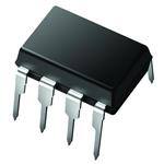
| 描述 | IC MOSFET DRIVER 6A HS 8DIP门驱动器 6A Power |
| 产品分类 | PMIC - MOSFET,电桥驱动器 - 外部开关集成电路 - IC |
| 品牌 | Microchip Technology |
| 产品手册 | |
| 产品图片 |
|
| rohs | 符合RoHS无铅 / 符合限制有害物质指令(RoHS)规范要求 |
| 产品系列 | 电源管理 IC,门驱动器,Microchip Technology TC429CPA- |
| 数据手册 | http://www.microchip.com/mymicrochip/filehandler.aspx?ddocname=en011675 |
| 产品型号 | TC429CPA |
| PCN组件/产地 | http://www.microchip.com/mymicrochip/NotificationDetails.aspx?id=5776&print=view |
| 上升时间 | 35 ns |
| 下降时间 | 35 ns |
| 产品 | MOSFET Gate Drivers |
| 产品目录页面 | |
| 产品种类 | 门驱动器 |
| 供应商器件封装 | 8-PDIP |
| 其它名称 | 158-1105 |
| 包装 | 管件 |
| 商标 | Microchip Technology |
| 安装类型 | 通孔 |
| 安装风格 | Through Hole |
| 封装 | Tube |
| 封装/外壳 | 8-DIP(0.300",7.62mm) |
| 封装/箱体 | PDIP-8 |
| 工作温度 | 0°C ~ 70°C |
| 工厂包装数量 | 60 |
| 延迟时间 | 53ns |
| 最大功率耗散 | 730 mW |
| 最大工作温度 | + 70 C |
| 最小工作温度 | 0 C |
| 标准包装 | 60 |
| 激励器数量 | 1 Driver |
| 电压-电源 | 7 V ~ 18 V |
| 电流-峰值 | 6A |
| 电源电压-最大 | 18 V |
| 电源电压-最小 | 7 V |
| 电源电流 | 8 mA |
| 类型 | Low Side |
| 输入类型 | 反相 |
| 输出数 | 1 |
| 输出端数量 | 1 |
| 配置 | 低端 |
| 配置数 | 1 |
| 高压侧电压-最大值(自举) | - |


- 商务部:美国ITC正式对集成电路等产品启动337调查
- 曝三星4nm工艺存在良率问题 高通将骁龙8 Gen1或转产台积电
- 太阳诱电将投资9.5亿元在常州建新厂生产MLCC 预计2023年完工
- 英特尔发布欧洲新工厂建设计划 深化IDM 2.0 战略
- 台积电先进制程称霸业界 有大客户加持明年业绩稳了
- 达到5530亿美元!SIA预计今年全球半导体销售额将创下新高
- 英特尔拟将自动驾驶子公司Mobileye上市 估值或超500亿美元
- 三星加码芯片和SET,合并消费电子和移动部门,撤换高东真等 CEO
- 三星电子宣布重大人事变动 还合并消费电子和移动部门
- 海关总署:前11个月进口集成电路产品价值2.52万亿元 增长14.8%


PDF Datasheet 数据手册内容提取
M TC429 6A Single High-Speed, CMOS Power MOSFET Driver Features General Description • High Peak Output Current: 6A The TC429 is a high-speed, single output, CMOS-level • Wide Input Supply Voltage Operating Range: translator and driver. Designed specifically to drive highly capacitive power MOSFET gates, the TC429 - 7V to 18V features a 2.5Ω output impedance and 6A peak output • High-Impedance CMOS Logic Input current drive. • Logic Input Threshold Independent of Supply A 2500pF capacitive load will be driven to 18V in Voltage 25nsec. The rapid switching times with large • Low Supply Current: capacitive loads minimize MOSFET switching power - With Logic ‘1’ Input – 5mA max. losses. - With Logic ‘0’ Input – 0.5mA max. A TTL/CMOS input logic level is translated into an • Output Voltage Swing Within 25mV of Ground output voltage swing that equals the supply voltage and or V DD will swing to within 25mV of ground or VDD. Input volt- • Short Delay Time: 75nsec max age swing may equal the supply voltage. Logic input • Available in the Space-Saving 8-Pin SOIC current is under 10µA, making direct interface to Package. CMOS/bipolar switch-mode power supply controllers • High Capacitive Load Drive Capability: easy. Input “speed-up” capacitors are not required. - t , t = 35nsec max with The CMOS design minimizes quiescent power supply RISE FALL C = 2500pF current. With a logic ‘1’ input, power supply current is LOAD 5mA maximum and decreases to 0.5mA for logic ‘0’ Applications inputs. For dual output MOSFET drivers, see the TC426/ • Switch-Mode Power Supplies TC427/TC428 (DS21415), TC4426/TC4427/TC4428 • CCD Drivers (DS21422) and TC4426A/TC4427A/TC4428A • Pulse Transformer Drive (DS21423) data sheets. • Class D Switching Amplifiers For non-inverting applications, or applications requiring Package Types latch-up protection, see the TC4420/TC4429 (DS21419) data sheet. CERDIP/PDIP/SOIC V 1 8 V DD DD INPUT 2 7 OUTPUT NC 3 6 OUTPUT GND 4 TC429 5 GND NC = No Internal Connection Note: Duplicate pins must both be connected for proper operation. 2003 Microchip Technology Inc. DS21416C-page 1
TC429 Functional Block Diagram 1,8 V DD 300mV 6,7 Output 2 Input Effective Input C = 38pF TC429 4,5 GND DS21416C-page 2 2003 Microchip Technology Inc.
TC429 1.0 ELECTRICAL PIN FUNCTION TABLE CHARACTERISTICS Symbol Description Absolute Maximum Ratings † V Supply input, 7V to 18V DD Supply Voltage.....................................................+20V INPUT Control input. TTL/CMOS compatible logic input Input Voltage, Any Terminal ...................................V + 0.3V to GND – 0.3V NC No connection DD Power Dissipation (T ≤ 70°C) GND Ground A PDIP............................................................730mW GND Ground CERDIP.......................................................800mW OUTPUT CMOS push-pull, common to pin 7 SOIC............................................................470mW OUTPUT CMOS push-pull, common to pin 6 Storage Temperature Range..............-65°C to +150°C Maximum Junction Temperature, T ...............+150°C VDD Supply input, 7V to 18V J † Stresses above those listed under "Absolute Maximum Ratings" may cause permanent damage to the device. These are stress ratings only and functional operation of the device at these or any other conditions above those indicated in the operation sections of the specifications is not implied. Exposure to Absolute Maximum Rating conditions for extended periods may affect device reliability. DC ELECTRICAL CHARACTERISTICS Electrical Specifications: Unless otherwise noted, T = +25°C with 7V ≤ V ≤ 18V. A DD Parameters Sym Min Typ Max Units Conditions Input Logic ‘1’, High Input Voltage V 2.4 1.8 — V IH Logic ‘0’, Low Input Voltage V — 1.3 0.8 V IL Input Current I -10 — 10 µA 0V ≤ V ≤ V IN IN DD Output High Output Voltage V V – 0.025 — — V OH DD Low Output Voltage V — — 0.025 V OL Output Resistance R — 1.8 2.5 Ω V = 0.8V, O IN V = 10mA, V = 18V OUT DD — 1.5 2.5 V = 2.4V, IN V = 10mA, V = 18V OUT DD Peak Output Current I — 6.0 — A V = 18V, Figure4-4 PK DD Latch-Up Protection I — 0.5 — A Duty cycle ≤ 2%, t ≤ 300µsec, REV Withstand Reverse Current V = 16V DD Switching Time (Note1) Rise Time t — 23 35 nsec C = 2500pF, Figure4-1 R L Fall Time t — 25 35 nsec C = 2500pF, Figure4-1 F L Delay Time t — 53 75 nsec Figure4-1 D1 Delay Time t — 60 75 nsec Figure4-1 D2 Power Supply Power Supply Current I — 3.5 5.0 mA V = 3V S IN — 0.3 0.5 V = 0V IN Note 1: Switching times ensured by design. 2003 Microchip Technology Inc. DS21416C-page 3
TC429 DC ELECTRICAL CHARACTERISTICS (CONTINUED) Electrical Specifications: Unless otherwise noted, over operating temperature range with 7V ≤ V ≤ 18V. DD Parameters Sym Min Typ Max Units Conditions Input Logic ‘1’, High Input Voltage V 2.4 — — V IH Logic ‘0’, Low Input Voltage V — — 0.8 V IL Input Current I -10 — 10 µA 0V ≤ V ≤ V IN IN DD Output High Output Voltage V V – 0.025 — — V OH DD Low Output Voltage V — — 0.025 V OL Output Resistance R — — 5.0 Ω V = 0.8V, O IN V = 10mA, V = 18V OUT DD — — 5.0 V = 2.4V, IN V = 10mA, V = 18V OUT DD Switching Time (Note1) Rise Time t — — 70 nsec C = 2500pF, Figure4-1 R L Fall Time t — — 70 nsec C = 2500pF, Figure4-1 F L Delay Time t — — 100 nsec Figure4-1 D1 Delay Time t — — 120 nsec Figure4-1 D2 Power Supply Power Supply Current I — — 12 mA V = 3V S IN — — 1.0 V = 0V IN Note 1: Switching times ensured by design. TEMPERATURE CHARACTERISTICS Electrical Specifications: Unless otherwise noted, T = +25°C with 7V ≤ V ≤ 18V. A DD Parameters Sym Min Typ Max Units Conditions Temperature Ranges Specified Temperature Range (C) T 0 — +70 ºC A Specified Temperature Range (E) T -40 — +85 ºC A Specified Temperature Range (M) T -55 — +125 ºC A Maximum Junction Temperature T — — +150 ºC J Storage Temperature Range T -65 — +150 ºC A Package Thermal Resistances Thermal Resistance, 8L-CERDIP θ — 150 — ºC/W JA Thermal Resistance, 8L-PDIP θ — 125 — ºC/W JA Thermal Resistance, 8L-SOIC θ — 155 — ºC/W JA DS21416C-page 4 2003 Microchip Technology Inc.
TC429 2.0 TYPICAL PERFORMANCE CURVES Note: The graphs and tables provided following this note are a statistical summary based on a limited number of samples and are provided for informational purposes only. The performance characteristics listed herein are not tested or guaranteed. In some graphs or tables, the data presented may be outside the specified operating range (e.g., outside specified power supply range) and therefore outside the warranted range. Note: Unless otherwise indicated, T = +25°C with 7V ≤ V ≤ 18V. A DD 60 70 TA = +25°C TA = +25°C 50 CL = 2500 pF A) 60 VDD = +15V m c) NT ( 50 E (nse40 URRE 40 M C 30 TI30 tF LY 400 kHz PP 20 U 200 kHz 20 tR S 10 20 kHz 10 0 5 10 15 20 10 100 1K 10K SUPPLY VOLTAGE (V) CAPACITIVE LOAD (pF) FIGURE 2-1: Rise/Fall Times vs. Supply FIGURE 2-4: Supply Current vs. Voltage. Capacitive Load. 60 90 CL = 2500 pF CL = 2500 pF VDD = +15V VDD = +15V 50 80 c) c) se e40 n 70 ns E ( ME ( tF TIM tD2 TI30 tR AY 60 L E 20 D 50 tD1 10 40 -50 -25 0 25 50 75 100125150 -50 -25 0 25 50 75 100125150 TEMPERATURE (°C) TEMPERATURE (°C) FIGURE 2-2: Rise/Fall Times vs. FIGURE 2-5: Delay Times vs. Temperature. Temperature. 100 140 TA = +25°C TA = +25°C VDD = +15V CL = 2500 pF 120 tF ec) c) ns E (nse10 tR TIME (100 M Y TI A 80 L E D tD2 60 tD1 1 40 100 1K 10K 5 10 15 20 CAPACITIVE LOAD (pF) SUPPLY VOLTAGE (V) FIGURE 2-3: Rise/Fall Times vs. FIGURE 2-6: Delay Times vs. Supply Capacitive Load. Voltage. 2003 Microchip Technology Inc. DS21416C-page 5
TC429 Note: Unless otherwise indicated, T = +25°C with 7V ≤ V ≤ 18V. A DD . 50 20 TA = +25°C TA = +25°C mA)40 CL = 2500 pF 10V V)15 HY≈S3T1E0R mEVSIS NT ( 15V GE ( E30 A R T 300 mV CUR VDD = 18V VOL10 PLY 20 PUT 200 mV UP UT 5 S10 O 5V 0 1 10 100 1K 0 0.250.500.75 1 1.251.501.75 2 FREQUENCY (kHz) INPUT VOLTAGE (V) FIGURE 2-7: Supply Current vs. FIGURE 2-10: Voltage Transfer Frequency. Characterstics. 4 400 TA = +25°C TA = +25°C RL = ∞ A) INPUT LOGIC "1" V) m m300 T ( E ( VDD = 5V N G E A CURR2 VOLT200 10V 15V LY UT UPP UTP100 18V S O 0 4 8 12 16 20 0 20 40 60 80 100 SUPPLY VOLTAGE (V) SOURCE CURRENT (mA) FIGURE 2-8: Supply Current vs. Supply FIGURE 2-11: High Output Voltage Voltage. (V -V ) vs. Output Source Current. DD OH 4 VRDL D= =∞ +18°C 400 TA = +25°C A) INPUT LOGIC "1" V) m m300 NT ( GE ( VDD = 5V URRE OLTA200 Y C3 T V 10V 15V L U P P UP UT100 S O 18V 2 -75-50 -25 0 25 50 75 100125150 0 20 40 60 80 100 TEMPERATURE (°C) SINK CURRENT (mA) FIGURE 2-9: Supply Current vs. FIGURE 2-12: Low Output Voltage vs. Temperature. Output Sink Current. DS21416C-page 6 2003 Microchip Technology Inc.
TC429 3.0 PIN DESCRIPTIONS The descriptions of the pins are listed in Table3-1. TABLE 3-1: PIN FUNCTION TABLE Pin No. Symbol Description 1 V Supply input, 7V to 18V DD 2 INPUT Control input. TTL/CMOS compatible logic input 3 NC No connection 4 GND Ground 5 GND Ground 6 OUTPUT CMOS push-pull output, common to pin 7 7 OUTPUT CMOS push-pull output, common to pin 6 8 V Supply input, 7V to 18V DD 3.1 Supply Input (V ) 3.3 CMOS Push-Pull Output DD (OUTPUT) The V input is the bias supply for the MOSFET driver DD and is rated for 7.0V to 18V with respect to the ground The MOSFET driver output is a low-impedance, CMOS pin. The VDD input should be bypassed to ground with push-pull style output, capable of driving a capacitive a local ceramic capacitor. The value of the capacitor load with 6.0A peak currents. should be chosen based on the capacitive load that is being driven. A value of 1.0µF is suggested. 3.4 Ground (GND) 3.2 Control Input (INPUT) The ground pins are the return path for the bias current and for the high peak currents that discharge the load The MOSFET driver input is a high-impedance, capacitor. The ground pins should be tied into a ground TTL/CMOS compatible input. The input also has plane or have very short traces to the bias supply 300mV of hysteresis between the high and low thresh- source return. olds that prevents output glitching even when the rise and fall time of the input signal is very slow. 3.5 No Connect (NC) No connection. 2003 Microchip Technology Inc. DS21416C-page 7
TC429 4.0 APPLICATIONS INFORMATION V = 18V DD 4.1 Supply Bypassing Charging and discharging large capacitive loads 1µF 0.1µF quickly requires large currents. For example, charging a 2500pF load to 18V in 25nsec requires a 1.8A 1, 8 current from the device's power supply. To ensure low supply impedance over a wide frequency range, a parallel capacitor combination is recom- 2 6, 7 Input Output mended for supply bypassing. Low-inductance ceramic disk capacitors with short lead lengths (< 0.5in.) CL = 2500pF TC429 should be used. A 1µF film capacitor in parallel with one or two 0.1µF ceramic disk capacitors normally 4, 5 Input: 100kHz, provides adequate bypassing. square wave, t = t ≤ 10nsec RISE FALL 4.2 Grounding +5V 90% The high-current capability of the TC429 demands careful PC board layout for best performance. Since Input the TC429 is an inverting driver, any ground lead 10% 0V impedance will appear as negative feedback that can tD1 tD2 degrade switching speed. The feedback is especially 18V tF tR noticeable with slow rise-time inputs, such as those 90% 90% produced by an open-collector output with resistor pull- Output up. The TC429 input structure includes about 300mV 10% 10% of hysteresis to ensure clean transitions and freedom 0V from oscillation, but attention to layout is still recommended. FIGURE 4-1: Inverting Driver Switching Time Test Circuit. Figure4-3 shows the feedback effect in detail. As the TC429 input begins to go positive, the output goes negative and several amperes of current flow in the ground lead. A PC trace resistance of as little as 0.05Ω can produce hundreds of millivolts at the TC429 ground INPUT pins. If the driving logic is referenced to power ground, V) DI the effective logic input level is reduced and oscillations V/ may result. E (5 G To ensure optimum device performance, separate TA OUTPUT L ground traces should be provided for the logic and VO CL = 2500pF power connections. Connecting logic ground directly to VS = 18V the TC429 GND pins ensures full logic drive to the input and fast output switching. Both GND pins should be 5V 100ns connected to power ground. TIME (100ns/DIV) CL = 2500pF VS = 7V V) DI INPUT V/ 5 E ( G A T L O V OUTPUT 5V 100ns TIME (100ns/DIV) FIGURE 4-2: Switching Speed. DS21416C-page 8 2003 Microchip Technology Inc.
TC429 +18V +18V TC429 1µF 1µF 18V 18V 2.4V TEK Current 2.4V TEK Current 1 Probe 6302 1 Probe 6302 0V 2 8 6,7 0V 0V 2 8 6,7 0V 0.1µF 4 5 0.1µF 2500pF 0.1µF 4 5 0.1µF 2500pF Logic TC429 Ground 6A 300mV PC Trace Resistance = 0.05Ω FIGURE 4-4: Peak Output Current Test Power Ground Circuit. 4.4 Power Dissipation FIGURE 4-3: Switching Time Degradation CMOS circuits usually permit the user to ignore power Due To Negative Feedback. dissipation. Logic families such as the 4000 and 74C have outputs that can only supply a few milliamperes of 4.3 Input Stage current, and even shorting outputs to ground will not force enough current to destroy the device. The TC429, The input voltage level changes the no-load or however, can source or sink several amperes and drive quiescent supply current. The N-channel MOSFET large capacitive loads at high frequency. Since the input stage transistor drives a 3mA current source package power dissipation limit can easily be load. With a logic ‘1’ input, the maximum quiescent exceeded, some attention should be given to power supply current is 5mA. Logic ‘0’ input level signals dissipation when driving low-impedance loads and/or reduce quiescent current to 500µA maximum. operating at high frequency. The TC429 input is designed to provide 300mV of The supply current versus frequency and supply hysteresis, providing clean transitions and minimizing current versus capacitive load characteristic curves will output stage current spiking when changing states. aid in determining power dissipation calculations. Input voltage levels are approximately 1.5V, making the Table4-1 lists the maximum operating frequency for device TTL-compatible over the 7V to 18V operating several power supply voltages when driving a 2500pF supply range. Input pin current draw is less than 10µA load. More accurate power dissipation figures can be over this range. obtained by summing the three components that make The TC429 can be directly driven by TL494, SG1526/ up the total device power dissipation. 1527, SG1524, SE5560 or similar switch-mode Input signal duty cycle, power supply voltage and powersupply integrated circuits. By off-loading the capacitive load influence package power dissipation. power-driving duties to the TC429, the power supply Given power dissipation and package thermal resis- controller can operate at lower dissipation, improving tance, the maximum ambient operation temperature performance and reliability. iseasily calculated. The 8-pin CERDIP junction-to- ambient thermal resistance is 150°C/W. At +25°C, the package is rated at 800mW maximum dissipation. Maximum allowable junction temperature is +150°C. Three components make up total package power dissipation: • Capacitive load dissipation (P ) C • Quiescent power (P ) Q • Transition power (P ) T The capacitive load-caused dissipation is a direct function of frequency, capacitive load and supply voltage. 2003 Microchip Technology Inc. DS21416C-page 9
TC429 The device capacitive load dissipation is: Note: Ambient operating temperature should not EQUATION exceed +85ºC for EPA or EOA devices or 2 +125ºC for MJA devices. P = fCV C S TABLE 4-1: MAXIMUM OPERATING Where: FREQUENCIES f = Switching frequency C = Capacitive load V f V = Supply voltage S MAX S 18V 500kHz Quiescent power dissipation depends on input signal 15V 700kHz duty cycle. A logic low input results in a low-power 10V 1.3MHz dissipation mode with only 0.5mA total current drain. Logic-high signals raise the current to 5mA maximum. 5V >2MHz The quiescent power dissipation is: Conditions: EQUATION 1. CERDIP Package (θJA =150°C/W) 2. T = +25°C A PQ = VS(D(IH)+(1–D)IL) 3. CL = 2500pF Where: I = Quiescent current with input high H (5mA max) IL = Quiescent current with input low 5V/DIV INPUT (0.5mA max) D = Duty cycle 500mV/DIV (5 AMP/DIV) Transition power dissipation arises because the output OUTPUT stage N- and P-channel MOS transistors are ON simultaneously for a very short period when the output changes. VS = 18V The device transition power dissipation is approxi- RL = 0.1Ω mately: 5V 500mV 5µs EQUATION TIME (5µs/DIV) –9 PT = fVS3.3×10 A•Sec FIGURE 4-5: Peak Output Current Capability. An example shows the relative magnitude for each item. 4.5 POWER-ON OSCILLATION C = 2500pF Note: It is extremely important that all MOSFET V = 15V S driver applications be evaluated for the D = 50% possibility of having high-power oscillations f = 200kHz occur during the power-on cycle. P = Package power dissipation: Power-on oscillations are due to trace size, layout and D = P + P + P component placement. A ‘quick fix’ for most applica- C T Q = 113mW + 10mW + 41mW tions that exhibit power-on oscillation problems is to = 164mW place approximately 10kΩ in series with the input of the MOSFET driver. Maximum ambient operating temperature: = T – θ (P ) J JA D = 150ºC - (150ºC/W)(0.164W) = 125°C Where: T = Maximum allowable junction temperature J (+150°C) θ = Junction-to-ambient thermal resistance JA (150°C/W, CERDIP) DS21416C-page 10 2003 Microchip Technology Inc.
TC429 5.0 PACKAGING INFORMATION 5.1 Package Marking Information 8-Lead PDIP (300 mil) Example: XXXXXXXX TC429CPA NNN 057 YYWW 0350 8-Lead CERDIP (300 mil) Example: XXXXXXXX TC429MJA NNN 057 YYWW 0350 8-Lead SOIC (150 mil) Example: XXXXXXXX TC429 XXXXYYWW EOA0350 NNN 057 Legend: XX...X Customer specific information* YY Year code (last 2 digits of calendar year) WW Week code (week of January 1 is week ‘01’) NNN Alphanumeric traceability code Note: In the event the full Microchip part number cannot be marked on one line, it will be carried over to the next line thus limiting the number of available characters for customer specific information. * Standard marking consists of Microchip part number, year code, week code, traceability code (facility code, mask rev#, and assembly code). For marking beyond this, certain price adders apply. Please check with your Microchip Sales Office. 2003 Microchip Technology Inc. DS21416C-page 11
TC429 8-Lead Plastic Dual In-line (PA) – 300 mil (PDIP) E1 D 2 n 1 α E A A2 L c A1 β B1 p eB B Units INCHES* MILLIMETERS Dimension Limits MIN NOM MAX MIN NOM MAX Number of Pins n 8 8 Pitch p .100 2.54 Top to Seating Plane A .140 .155 .170 3.56 3.94 4.32 Molded Package Thickness A2 .115 .130 .145 2.92 3.30 3.68 Base to Seating Plane A1 .015 0.38 Shoulder to Shoulder Width E .300 .313 .325 7.62 7.94 8.26 Molded Package Width E1 .240 .250 .260 6.10 6.35 6.60 Overall Length D .360 .373 .385 9.14 9.46 9.78 Tip to Seating Plane L .125 .130 .135 3.18 3.30 3.43 Lead Thickness c .008 .012 .015 0.20 0.29 0.38 Upper Lead Width B1 .045 .058 .070 1.14 1.46 1.78 Lower Lead Width B .014 .018 .022 0.36 0.46 0.56 Overall Row Spacing § eB .310 .370 .430 7.87 9.40 10.92 Mold Draft Angle Top a 5 10 15 5 10 15 Mold Draft Angle Bottom b 5 10 15 5 10 15 * Controlling Parameter § Significant Characteristic Notes: Dimensions D and E1 do not include mold flash or protrusions. Mold flash or protrusions shall not exceed .010” (0.254mm) per side. JEDEC Equivalent: MS-001 Drawing No. C04-018 DS21416C-page 12 2003 Microchip Technology Inc.
TC429 8-Lead Ceramic Dual In-line – 300 mil (CERDIP) E1 2 n 1 D E A2 A c L eB B1 B A1 p Units INCHES* MILLIMETERS Dimension Limits MIN NOM MAX MIN NOM MAX Number of Pins n 8 8 Pitch p .100 2.54 Top to Seating Plane A .160 .180 .200 4.06 4.57 5.08 Standoff § A1 .020 .030 .040 0.51 0.77 1.02 Shoulder to Shoulder Width E .290 .305 .320 7.37 7.75 8.13 Ceramic Pkg. Width E1 .230 .265 .300 5.84 6.73 7.62 Overall Length D .370 .385 .400 9.40 9.78 10.16 Tip to Seating Plane L .125 .163 .200 3.18 4.13 5.08 Lead Thickness c .008 .012 .015 0.20 0.29 0.38 Upper Lead Width B1 .045 .055 .065 1.14 1.40 1.65 Lower Lead Width B .016 .018 .020 0.41 0.46 0.51 Overall Row Spacing eB .320 .360 .400 8.13 9.15 10.16 *Controlling Parameter JEDEC Equivalent: MS-030 Drawing No. C04-010 2003 Microchip Technology Inc. DS21416C-page 13
TC429 8-Lead Plastic Small Outline (OA) – Narrow, 150 mil (SOIC) E E1 p D 2 B n 1 h α 45° c A A2 φ β L A1 Units INCHES* MILLIMETERS Dimension Limits MIN NOM MAX MIN NOM MAX Number of Pins n 8 8 Pitch p .050 1.27 Overall Height A .053 .061 .069 1.35 1.55 1.75 Molded Package Thickness A2 .052 .056 .061 1.32 1.42 1.55 Standoff § A1 .004 .007 .010 0.10 0.18 0.25 Overall Width E .228 .237 .244 5.79 6.02 6.20 Molded Package Width E1 .146 .154 .157 3.71 3.91 3.99 Overall Length D .189 .193 .197 4.80 4.90 5.00 Chamfer Distance h .010 .015 .020 0.25 0.38 0.51 Foot Length L .019 .025 .030 0.48 0.62 0.76 Foot Angle φ 0 4 8 0 4 8 Lead Thickness c .008 .009 .010 0.20 0.23 0.25 Lead Width B .013 .017 .020 0.33 0.42 0.51 Mold Draft Angle Top α 0 12 15 0 12 15 Mold Draft Angle Bottom β 0 12 15 0 12 15 * Controlling Parameter § Significant Characteristic Notes: Dimensions D and E1 do not include mold flash or protrusions. Mold flash or protrusions shall not exceed .010” (0.254mm) per side. JEDEC Equivalent: MS-012 Drawing No. C04-057 DS21416C-page 14 2003 Microchip Technology Inc.
TC429 PRODUCT IDENTIFICATION SYSTEM To order or obtain information, e.g., on pricing or delivery, refer to the factory or the listed sales office. PART NO. X /XX Examples: Device Temperature Package a) TC429CPA: 6A Single MOSFET driver, Range PDIP package, 0°C to +70°C. b) TC429MJA: 6A Single MOSFET driver, CERDIP package, -55°C to +125°C. Device: TC429: 6A Single MOSFET Driver c) TC429EPA: 6A Single MOSFET driver, PDIP package, -40°C to +85°C. Temperature Range: C = 0°C to +70°C d) TC429EOA713: Tape and Reel, E = -40°C to +85°C 6A Single MOSFET driver, SOIC package, - M = -55°C to +125°C (CERDIP only) 40°C to +85°C. Package: JA = Plastic CERDIP, (300 mil Body), 8-lead OA = Plastic SOIC, (150 mil Body), 8-lead * OA713= Plastic SOIC, (150 mil Body), 8-lead * (Tape and Reel) PA = Plastic DIP (300 mil Body), 8-lead * SOIC package offered in E-Temp only Sales and Support Data Sheets Products supported by a preliminary Data Sheet may have an errata sheet describing minor operational differences and recom- mended workarounds. To determine if an errata sheet exists for a particular device, please contact one of the following: 1. Your local Microchip sales office 2. The Microchip Corporate Literature Center U.S. FAX: (480) 792-7277 3. The Microchip Worldwide Site (www.microchip.com) Please specify which device, revision of silicon and Data Sheet (include Literature #) you are using. Customer Notification System Register on our web site (www.microchip.com/cn) to receive the most current information on our products. 2003 Microchip Technology Inc. DS21416C-page15
TC429 NOTES: DS21416C-page 16 2003 Microchip Technology Inc.
Note the following details of the code protection feature on Microchip devices: • Microchip products meet the specification contained in their particular Microchip Data Sheet. • Microchip believes that its family of products is one of the most secure families of its kind on the market today, when used in the intended manner and under normal conditions. • There are dishonest and possibly illegal methods used to breach the code protection feature. All of these methods, to our knowledge, require using the Microchip products in a manner outside the operating specifications contained in Microchip's Data Sheets. Most likely, the person doing so is engaged in theft of intellectual property. • Microchip is willing to work with the customer who is concerned about the integrity of their code. • Neither Microchip nor any other semiconductor manufacturer can guarantee the security of their code. Code protection does not mean that we are guaranteeing the product as “unbreakable.” Code protection is constantly evolving. We at Microchip are committed to continuously improving the code protection features of our products. Attempts to break microchip’s code protection feature may be a violation of the Digital Millennium Copyright Act. If such acts allow unauthorized access to your software or other copyrighted work, you may have a right to sue for relief under that Act. Information contained in this publication regarding device Trademarks applications and the like is intended through suggestion only and may be superseded by updates. It is your responsibility to The Microchip name and logo, the Microchip logo, KEELOQ, ensure that your application meets with your specifications. No MPLAB, PIC, PICmicro, PICSTART, PRO MATE and representation or warranty is given and no liability is assumed PowerSmart are registered trademarks of Microchip Technology by Microchip Technology Incorporated with respect to the Incorporated in the U.S.A. and other countries. accuracy or use of such information, or infringement of patents FilterLab, microID, MXDEV, MXLAB, PICMASTER, SEEVAL or other intellectual property rights arising from such use or and The Embedded Control Solutions Company are registered otherwise. Use of Microchip’s products as critical components in trademarks of Microchip Technology Incorporated in the U.S.A. life support systems is not authorized except with express written approval by Microchip. No licenses are conveyed, Accuron, Application Maestro, dsPIC, dsPICDEM, implicitly or otherwise, under any intellectual property rights. dsPICDEM.net, ECONOMONITOR, FanSense, FlexROM, fuzzyLAB, In-Circuit Serial Programming, ICSP, ICEPIC, microPort, Migratable Memory, MPASM, MPLIB, MPLINK, MPSIM, PICC, PICkit, PICDEM, PICDEM.net, PowerCal, PowerInfo, PowerMate, PowerTool, rfLAB, rfPIC, Select Mode, SmartSensor, SmartShunt, SmartTel and Total Endurance are trademarks of Microchip Technology Incorporated in the U.S.A. and other countries. Serialized Quick Turn Programming (SQTP) is a service mark of Microchip Technology Incorporated in the U.S.A. All other trademarks mentioned herein are property of their respective companies. © 2003, Microchip Technology Incorporated, Printed in the U.S.A., All Rights Reserved. Printed on recycled paper. Microchip received QS-9000 quality system certification for its worldwide headquarters, design and wafer fabrication facilities in Chandler and Tempe, Arizona in July 1999 and Mountain View, California in March 2002. The Company’s quality system processes and procedures are QS-9000 compliant for its PICmicro® 8-bit MCUs, KEELOQ® code hopping devices, Serial EEPROMs, microperipherals, non-volatile memory and analog products. In addition, Microchip’s quality system for the design and manufacture of development systems is ISO 9001 certified. 2003 Microchip Technology Inc. DS21416C - page 17
M WORLDWIDE SALES AND SERVICE AMERICAS ASIA/PACIFIC Japan Corporate Office Australia Microchip Technology Japan K.K. Benex S-1 6F 2355 West Chandler Blvd. Microchip Technology Australia Pty Ltd 3-18-20, Shinyokohama Chandler, AZ 85224-6199 Marketing Support Division Kohoku-Ku, Yokohama-shi Tel: 480-792-7200 Fax: 480-792-7277 Suite 22, 41 Rawson Street Kanagawa, 222-0033, Japan Technical Support: 480-792-7627 Epping 2121, NSW Tel: 81-45-471- 6166 Fax: 81-45-471-6122 Web Address: http://www.microchip.com Australia Korea Atlanta Tel: 61-2-9868-6733 Fax: 61-2-9868-6755 China - Beijing Microchip Technology Korea 3780 Mansell Road, Suite 130 168-1, Youngbo Bldg. 3 Floor Alpharetta, GA 30022 Microchip Technology Consulting (Shanghai) Samsung-Dong, Kangnam-Ku Tel: 770-640-0034 Fax: 770-640-0307 Co., Ltd., Beijing Liaison Office Seoul, Korea 135-882 Unit 915 Boston Tel: 82-2-554-7200 Fax: 82-2-558-5934 Bei Hai Wan Tai Bldg. 2 Lan Drive, Suite 120 No. 6 Chaoyangmen Beidajie Singapore Westford, MA 01886 Beijing, 100027, No. China Microchip Technology Singapore Pte Ltd. Tel: 978-692-3848 Fax: 978-692-3821 Tel: 86-10-85282100 Fax: 86-10-85282104 200 Middle Road Chicago China - Chengdu #07-02 Prime Centre Singapore, 188980 333 Pierce Road, Suite 180 Microchip Technology Consulting (Shanghai) Tel: 65-6334-8870 Fax: 65-6334-8850 Itasca, IL 60143 Co., Ltd., Chengdu Liaison Office Tel: 630-285-0071 Fax: 630-285-0075 Rm. 2401-2402, 24th Floor, Taiwan Microchip Technology (Barbados) Inc., Dallas Ming Xing Financial Tower No. 88 TIDU Street Taiwan Branch 4570 Westgrove Drive, Suite 160 Chengdu 610016, China 11F-3, No. 207 Addison, TX 75001 Tung Hua North Road Tel: 972-818-7423 Fax: 972-818-2924 Tel: 86-28-86766200 Fax: 86-28-86766599 Taipei, 105, Taiwan China - Fuzhou Detroit Tel: 886-2-2717-7175 Fax: 886-2-2545-0139 Microchip Technology Consulting (Shanghai) Tri-Atria Office Building Co., Ltd., Fuzhou Liaison Office EUROPE 32255 Northwestern Highway, Suite 190 Farmington Hills, MI 48334 Unit 28F, World Trade Plaza Austria No. 71 Wusi Road Tel: 248-538-2250 Fax: 248-538-2260 Fuzhou 350001, China Microchip Technology Austria GmbH Kokomo Tel: 86-591-7503506 Fax: 86-591-7503521 Durisolstrasse 2 A-4600 Wels 2767 S. Albright Road China - Hong Kong SAR Kokomo, Indiana 46902 Austria Microchip Technology Hongkong Ltd. Tel: 43-7242-2244-399 Tel: 765-864-8360 Fax: 765-864-8387 Unit 901-6, Tower 2, Metroplaza Fax: 43-7242-2244-393 Los Angeles 223 Hing Fong Road Denmark 18201 Von Karman, Suite 1090 Kwai Fong, N.T., Hong Kong Microchip Technology Nordic ApS Irvine, CA 92612 Tel: 852-2401-1200 Fax: 852-2401-3431 Regus Business Centre Tel: 949-263-1888 Fax: 949-263-1338 China - Shanghai Lautrup hoj 1-3 Phoenix Microchip Technology Consulting (Shanghai) Ballerup DK-2750 Denmark 2355 West Chandler Blvd. Co., Ltd. Tel: 45 4420 9895 Fax: 45 4420 9910 Chandler, AZ 85224-6199 Room 701, Bldg. B France Far East International Plaza Tel: 480-792-7966 Fax: 480-792-4338 Microchip Technology SARL No. 317 Xian Xia Road Parc d’Activite du Moulin de Massy San Jose Shanghai, 200051 43 Rue du Saule Trapu Microchip Technology Inc. Tel: 86-21-6275-5700 Fax: 86-21-6275-5060 Batiment A - ler Etage 2107 North First Street, Suite 590 China - Shenzhen 91300 Massy, France San Jose, CA 95131 Microchip Technology Consulting (Shanghai) Tel: 33-1-69-53-63-20 Fax: 33-1-69-30-90-79 Tel: 408-436-7950 Fax: 408-436-7955 Co., Ltd., Shenzhen Liaison Office Germany Toronto Rm. 1812, 18/F, Building A, United Plaza Microchip Technology GmbH 6285 Northam Drive, Suite 108 No. 5022 Binhe Road, Futian District Steinheilstrasse 10 Mississauga, Ontario L4V 1X5, Canada Shenzhen 518033, China D-85737 Ismaning, Germany Tel: 905-673-0699 Fax: 905-673-6509 Tel: 86-755-82901380 Fax: 86-755-82966626 Tel: 49-89-627-144-0 China - Qingdao Fax: 49-89-627-144-44 Rm. B505A, Fullhope Plaza, Italy No. 12 Hong Kong Central Rd. Microchip Technology SRL Qingdao 266071, China Via Quasimodo, 12 Tel: 86-532-5027355 Fax: 86-532-5027205 20025 Legnano (MI) India Milan, Italy Microchip Technology Inc. Tel: 39-0331-742611 Fax: 39-0331-466781 India Liaison Office United Kingdom Marketing Support Division Microchip Ltd. Divyasree Chambers 505 Eskdale Road 1 Floor, Wing A (A3/A4) Winnersh Triangle No. 11, O’Shaugnessey Road Wokingham Bangalore, 560 025, India Berkshire, England RG41 5TU Tel: 91-80-2290061 Fax: 91-80-2290062 Tel: 44 118 921 5869 Fax: 44-118 921-5820 03/25/03 DS21416C-page 18 2003 Microchip Technology Inc.
Mouser Electronics Authorized Distributor Click to View Pricing, Inventory, Delivery & Lifecycle Information: M icrochip: TC429EOA TC429EPA TC429CPA TC429EOA713