ICGOO在线商城 > 集成电路(IC) > PMIC - PFC(功率因数修正) > UC3855AN
 Datasheet下载
- 型号: UC3855AN
- 制造商: Texas Instruments
- 库位|库存: xxxx|xxxx
- 要求:
| 数量阶梯 | 香港交货 | 国内含税 |
| +xxxx | $xxxx | ¥xxxx |
查看当月历史价格
查看今年历史价格
UC3855AN产品简介:
ICGOO电子元器件商城为您提供UC3855AN由Texas Instruments设计生产,在icgoo商城现货销售,并且可以通过原厂、代理商等渠道进行代购。 UC3855AN价格参考。Texas InstrumentsUC3855AN封装/规格:PMIC - PFC(功率因数修正), PFC IC Average Current 500kHz 20-PDIP。您可以下载UC3855AN参考资料、Datasheet数据手册功能说明书,资料中有UC3855AN 详细功能的应用电路图电压和使用方法及教程。
UC3855AN 是由 Texas Instruments(德州仪器)生产的一款 PMIC - PFC(功率因数校正)控制器,广泛应用于高效率、高性能的电力电子设备中。以下是 UC3855AN 的主要应用场景:

 1. 工业电源
   - UC3855AN 常用于工业级开关电源的设计中,提供稳定的功率因数校正功能。例如,在 CNC 机床、工业机器人、自动化生产线等场景中,需要高效、可靠的电源供应,UC3855AN 可以确保系统在高负载下的稳定运行。
   - 在不间断电源(UPS)系统中,UC3855AN 能够优化输入功率因数,减少谐波失真,提高系统的整体效率。

 2. 通信设备
   - 在基站、路由器和交换机等通信设备中,UC3855AN 被用于 AC-DC 转换器的设计,以满足严格的功率因数要求。它能够有效降低输入电流的谐波成分,提升能源利用率,同时符合国际能效标准。

 3. 消费类电子产品
   - 高端电视、家用空调、洗衣机等大功率家电中,UC3855AN 能够实现高效的功率因数校正,减少对电网的干扰,同时降低能耗。
   - 在笔记本电脑适配器或游戏主机电源中,UC3855AN 提供了更高的转换效率和更小的体积设计可能性。

 4. 新能源领域
   - 在太阳能逆变器和风力发电系统中,UC3855AN 被用于前端功率因数校正电路,确保电能质量符合并网要求。
   - 电动汽车充电站中的充电桩也常使用 UC3855AN 来优化输入功率因数,保证充电过程的高效性和稳定性。

 5. 医疗设备
   - 在 X 光机、超声波设备和其他高精度医疗仪器中,UC3855AN 提供了精确的电源管理解决方案,确保设备在复杂工况下的稳定运行。

 总结
UC3855AN 的核心优势在于其高效的功率因数校正能力,适用于需要高功率密度、低谐波失真的应用场景。无论是工业、通信、消费电子还是新能源领域,UC3855AN 都能为系统提供可靠的电源支持,同时满足全球能效法规的要求。
| 参数 | 数值 |
| 产品目录 | 集成电路 (IC)半导体 |
| 描述 | IC PFC CTRLR AVERAGE CURR 20DIP功率因数校正 - PFC High Performance Preregulator |
| 产品分类 | |
| 品牌 | Texas Instruments |
| 产品手册 | |
| 产品图片 |
|
| rohs | 符合RoHS无铅 / 符合限制有害物质指令(RoHS)规范要求 |
| 产品系列 | 电源管理 IC,功率因数校正 - PFC,Texas Instruments UC3855AN- |
| 数据手册 | |
| 产品型号 | UC3855AN |
| 产品目录页面 | |
| 产品种类 | 功率因数校正 - PFC |
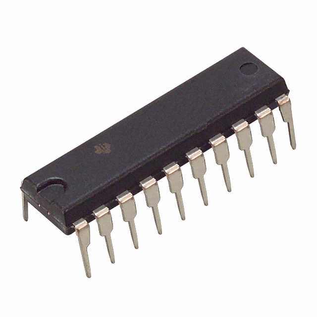
| 供应商器件封装 | 20-PDIP |
| 其它名称 | 296-11314-5 |
| 包装 | 管件 |
| 商标 | Texas Instruments |
| 安装类型 | 通孔 |
| 安装风格 | Through Hole |
| 封装 | Tube |
| 封装/外壳 | 20-DIP(0.300",7.62mm) |
| 封装/箱体 | PDIP-20 |
| 工作温度 | 0°C ~ 70°C |
| 工厂包装数量 | 20 |
| 开关频率 | 230 kHz |
| 最大工作温度 | + 70 C |
| 最小工作温度 | 0 C |
| 标准包装 | 20 |
| 模式 | 平均电流 |
| 电压-电源 | 15.5 V ~ 20 V |
| 电流-启动 | 150µA |
| 系列 | UC3855A |
| 频率-开关 | 500kHz |


- 商务部:美国ITC正式对集成电路等产品启动337调查
- 曝三星4nm工艺存在良率问题 高通将骁龙8 Gen1或转产台积电
- 太阳诱电将投资9.5亿元在常州建新厂生产MLCC 预计2023年完工
- 英特尔发布欧洲新工厂建设计划 深化IDM 2.0 战略
- 台积电先进制程称霸业界 有大客户加持明年业绩稳了
- 达到5530亿美元!SIA预计今年全球半导体销售额将创下新高
- 英特尔拟将自动驾驶子公司Mobileye上市 估值或超500亿美元
- 三星加码芯片和SET,合并消费电子和移动部门,撤换高东真等 CEO
- 三星电子宣布重大人事变动 还合并消费电子和移动部门
- 海关总署:前11个月进口集成电路产品价值2.52万亿元 增长14.8%


PDF Datasheet 数据手册内容提取
application UC2855A/B INFO UC3855A/B available High Performance Power Factor Preregulator FEATURES DESCRIPTION • ControlsBoostPWMtoNearUnity The UC3855A/B provides all the control features necessary for high PowerFactor power, high frequency PFC boost converters. The average current mode control method allows for stable, low distortion AC line current program- • FixedFrequencyAverageCurrent ming without the need for slope compensation. In addition, the UC3855 ModeControlMinimizesLineCurrent utilizes an active snubbing or ZVT (Zero Voltage Transition technique) to Distortion dramatically reduce diode recovery and MOSFET turn-on losses, result- • Built-inActiveSnubber(ZVT)allows inginlowerEMIemissionsandhigherefficiency. Boostconverterswitch- Operationto500kHz,improvedEMI ing frequencies up to 500kHz are now realizable, requiring only an andEfficiency additional small MOSFET, diode, and inductor to resonantly soft switch • InductorCurrentSynthesizerallows theboostdiodeandswitch.Averagecurrentsensingcanbeemployedus- SingleCurrentTransformerCurrent ing a simple resistive shunt or a current sense transformer. Using the cur- SenseforImprovedEfficiencyand rent sense transformer method, the internal current synthesizer circuit NoiseMargin bufferstheinductorcurrentduringtheswitchon-time,andreconstructsthe inductor current during the switch off-time. Improved signal to noise ratio • AccurateAnalogMultiplierwithLine and negligible current sensing losses make this an attractive solution for CompensatorallowsforUniversal higherpowerapplications. InputVoltageOperation • HighBandwidth(5MHz),LowOffset The UC3855A/B also features a single quadrant multiplier, squarer, and dividercircuitwhichprovidestheprogrammingsignalforthecurrentloop. CurrentAmplifier The internal multiplier current limit reduces output power during low line • OvervoltageandOvercurrent conditions. An overvoltage protection circuit disables both controller out- protection putsintheeventofaboostoutputOVcondition. • TwoUVLOThresholdOptions Low startup supply current, UVLO with hysteresis, a 1% 7.5V reference, • 150µAStartupSupplyCurrentTypical voltage amplifier with softstart, input supply voltage clamp, enable com- parator, and overcurrent comparator complete the list of features. Avail- • Precision1%7.5VReference ablepackagesinclude:20pinN,DW,Q,J,andL. BLOCK DIAGRAM LicensePatentfromPioneerMagnetics.PinnumbersrefertoDIL-20JorNpackages. UDG-94001-2 SLUS328BJUNE1998-REVISEDOctober2005
UC2855A/B UC3855A/B ABSOLUTE MAXIMUM RATINGS CONNECTION DIAGRAMS SupplyVoltageVCC..........................InternallyLimited PLCC-20&LCC-20(TopView) VCCSupplyClampCurrent.......................20mA QorL Package PFCGateDriverCurrent(continuous) ..............±0.5A PFCGateDriverCurrent(peak) ...................±1.5A ZVTDriveCurrent(continuous)...................±0.25A ZVTDriveCurrent(peak)........................±0.75A InputCurrent(IAC,RT,RVA) .......................5mA AnalogInputs(exceptPeakLimit)..............−0.3to10V PeakLimitInput ...........................−0.3to6.5V SoftstartSinkingCurrent.........................1.5mA StorageTemperature...................−65°Cto+150°C JunctionTemperature...................−55°Cto+150°C LeadTemperature(Soldering,10sec.).............+300°C Currentsarepositiveinto,negativeoutofthespecifiedtermi- nal.ConsultPackagingSectionofDatabookforthermallimita- tionsandconsiderationsofpackages.Allvoltagesare referencedtoGND. DIL–20(TopView) SOIC-20(TopView) JorNPackage DWPackage ELECTRICAL CHARACTERISTICS:Unlessotherwisespecified:VCC=18V,RVS=23k,CT=470pF,CI=150pF,VRMS =1.5V,IAC=100µA,I =0V,CAO=4V,VAOUT=3.5V,VSENSE=3V. –40°Cto85°C(UC2855A/B),0°Cto70°C SENSE (UC3855A/B). PARAMETER TESTCONDITIONS MIN TYP MAX UNITS Overall SupplyCurrent,OFF CAO,VAOUT=0V,VCC=UVLO−0.3V 150 500 µA SupplyCurrent,OPERATING 17 25 mA VCCTurn-OnThreshold UC3855A 15.5 17.5 V VCCTurn-OffThreshold UC3855A,B 9 10 V VCCTurn-OnThreshold UC3855B 10.5 10.8 V VCCClamp I(VCC)=I +5mA 18 20 22 V CC(on) VoltageAmplifier InputVoltage 2.9 3.1 V VSENSEBiasCurrent −500 25 500 nA OpenLoopGain V =2to5V 65 80 dB OUT VOUTHigh ILOAD=–300µA 5.75 6 6.25 V VOUTLow ILOAD=300µA 0.3 0.5 V OutputShortCircuit Current VOUT=0V 0.6 3 mA 2
UC2855A/B UC3855A/B ELECTRICAL CHARACTERISTICS:Unlessotherwisespecified:VCC=18V,RVS=23k,CT=470pF,CI=150pF,VRMS =1.5V,IAC=100µA,I =0V,CAO =4V,VAOUT=3.5V,VSENSE=3V.–40°Cto85°C(UC2855A/B),0°Cto70°C SENSE (UC3855A/B). PARAMETER TESTCONDITIONS MIN TYP MAX UNITS CurrentAmplifier InputOffsetVoltage V =−2.5V −4 4 mV CM InputBiasCurrent(Sense) V =2.5V −500 500 nA CM OpenLoopGain VCM =2.5V,VOUT=2to6V 80 110 dB VOUTHigh ILOAD=−500µA 6 V VOUTLow ILOAD=500µA 0.3 0.5 V OutputShortCircuitCurrent V =0V 1 3 mA OUT CommonModeRange −0.3 5 V GainBandwidthProduct F =100kHz,10mV,P–P,T =25°C 2.5 5 MHz IN A Reference OutputVoltage IREF=0mA,TA=25°C 7.388 7.5 7.613 V I =0mA 7.313 7.5 7.688 V REF LoadRegulation I =1to10mA −15 15 mV REF LineRegulation VCC=15to35V −10 10 mV ShortCircuitCurrent REF=0V 20 45 65 mA Oscillator InitialAccuracy T =25°C 170 200 230 kHz A VoltageStability V =12to18V 1 % CC TotalVariation Line,Temp. 160 240 kHz RampAmplitude(P–P) Outputsat0%dutycycle 4.7 5.7 V RampValleyVoltage 1.1 1.6 V Enable/OVP/CurrentLimit EnableThreshold 1.8 2.2 V OVPThreshold 7.5 7.66 V OVPHysteresis 200 400 600 mV OVPPropagationDelay 200 ns OVPInputBiasCurrent V=7.5V 1 10 µA PKLIMITThreshold 1.25 1.5 1.75 V PKLIMITInputCurrent VPKLIMIT=1.5V 100 µA PKLIMITProp.Delay 100 ns SoftStart SoftStartChargeCurrent -10 -13 -20 (cid:1)A SoftStartDischargeCurrent 2 10 20 mA Multiplier OutputCurrent-IACLimited IAC=100µA,VRMS=1V −235 −205 −175 µA OutputCurrent-Zero IAC=0µA −2 −0.2 2 µA OutputCurrent-PowerLimited VRMS=1.5V,VAOUT=5.5V −250 −209 −160 µA OutputCurrent VRMS=1.5V,VAOUT=2V −26 µA VRMS=1.5VVAOUT=5V −190 µA VRMS=5V,VAOUT=2V −3 µA VRMS=5V,VAOUT=5V −17 µA GainConstant RefertoNote1 −0.95 −0.85 −0.75 1/V 3
UC2855A/B UC3855A/B ELECTRICAL CHARACTERISTICS:Unlessotherwisespecified:VCC=18V,RVS=23k,CT=470pF,CI=150pF,VRMS =1.5V,IAC=100µA,I =0V,CAO=4V,VAOUT=3.5V,VSENSE=3V.–40°Cto85°C(UC2855A/B),0°Cto70°C SENSE (UC3855A/B). PARAMETER TESTCONDITIONS MIN TYP MAX UNITS GateDriverOutput OutputHighVoltage l =−200mA,VCC=15V 12 12.8 V OUT OutputLowVoltage l =200mA 1 2.2 V OUT OutputLowVoltage l =10mA 300 500 mV OUT OutputLow(UVLO) lOUT=50mA,VCC=0V 0.9 1.5 V OutputRISE/FALLTime CLOAD=1nF 35 ns OutputPeakCurrent CLOAD=10nF 0.5 1.5 A ZVT ZVSThreshold 2.3 2.6 2.9 V InputBiasCurrent V=2.5V,V =0 6 20 µA CT PropagationDelay MeasuredatZVTOUT 100 ns MaximumPulseWidth 400 ns OutputHighVoltage lOUT=−100mA,VCC=15V 12 12.8 V OutputLowVoltage l =100mA 1 2.2 V OUT l =10mA 300 900 mV OUT OutputLow(UVLO) l =50mA,V =0V 0.9 1.5 V OUT CC OutputRISE/FALLTime C =1nF 35 ns LOAD OutputPeakCurrent C =10nF 0.25 0.75 A LOAD CurrentSynthesizer IONtoCSOffset VION=0V 30 50 mV ClDischargeCurrent IAC=50µA 105 118 140 µA IAC=500µA 5 µA IACOffsetVoltage 0.3 0.65 1.1 V IONBufferSlewRate 10 V/µs IONInputBiasCurrent V =2V 2 15 µA ION RVSOutputVoltage 23kfromRVStoGND 2.87 3 3.13 V IAC•(VA –1.5V) Note1:Gainconstant(K)= OUT atV =1.5V,VA =5.5V. (V 2•IMO) RMS OUT RMS PIN DESCRIPTIONS CA This is the inverting input to the current amplifier. CI: The level shifted current sense signal is impressed Connect the required compensation components be- upon a capacitor connected between this pin and GND. tweenthispinandCAOUT.Thecommonmodeoperating The buffered current sense transformer signal charges rangeforthisinputisbetween−0.3Vand5V. the capacitor when the boost switch is on. When the switch is off, the current synthesizer discharges the ca- CAO: This is the output of the wide bandwidth current pacitor at a rate proportional to the dI/dt of the boost in- amplifier and one of the inputs to the PWM duty cycle ductor current. In this way, the discharge current is comparator.Theoutputsignalgeneratedbythisamplifier approximatelyequalto commands the PWM to force the correct input current. Theoutputcanswingfrom0.1Vto7.5V. 3V IAC – . RRVS 4 Discharging the CI capacitor in this fashion, a “recon- structed” version of the inductor current is generated us- ingonlyonecurrentsensetransformer. 4
UC2855A/B UC3855A/B PIN DESCRIPTIONS (cont.) CS:The reconstructed inductor current waveform gener- ION: This pin is the current sensing input. It should be ated on the CI pin is level shifted down a diode drop to connected to the secondary side output of a current this pin. Connect the current amplifier input resistor be- sensing transformer whose primary winding is in series tween CSand the inverting input of the current amplifier. with the boost switch. The resultant signal applied to this The waveform on this pin is compared to the multiplier inputisbufferedandlevelshiftedupadiodetotheCIca- output waveform through the average current sensing pacitor on the CI pin. The ION buffer has a source only current amplifier. The input to the peak current limiting output. Discharge of the CI cap is enabled through the comparator is also connected to this pin. A voltage level current synthesizer circuitry. The current sense trans- greater than 1.5 volts on this pin will trip the comparator former termination resistor should be designed to obtain anddisablethegatedriveroutput. a1Vinputsignalamplitudeatpeakswitchcurrent. OVP:This pin senses the boost output voltage through a CT:Acapacitor from CT to GND sets the PWM oscillator voltagedivider.TheenablecomparatorinputisTTLcom- frequencyaccordingtothefollowingequation: patible and can be used as a remote shutdown port. A 1 f ≈ . voltage level below 1.8V, disables VREF, oscillator, and 11200•CT the PWM circuitry via the enable comparator. Between 1.8V and VREF (7.5V) the UC is enabled. Voltage levels Use a high quality ceramic capacitor with low ESL and above7.5VwillsetthePWMlatchviathehystereticOVP ESR for best results. A minimum CT value of 200pF in- comparator and disable both ZVTOUT and GTOUT until sures good accuracy and less susceptibility to circuit lay- the OVP level has decayed by the nominal hysteresis of out parasitics. The oscillator and PWM are designed to 400mV. If the voltage divider is designed to initiate an providepracticaloperationto500kHz. OVP fault at 5% of OV, the internal hysteresis enables normal operation again when the output voltage has GND: All voltages are measured with respect to this pin. reached its nominal regulation level. Both the OVP and All bypass and timing capacitors connected to GND enable comparators have direct logical connections to shouldhaveleadsasshortanddirectaspossible. thePWMoutputandexhibittypicalpropagationdelaysof GTOUT: The output of the PWM is a 1.5A peak totem 200ns. pole MOSFET gate driver on GTOUT. A series resistor REF: REF is the output of the precision reference. The between GTOUT and the MOSFET gate of at least 10 output is capable of supplying 25mA to peripheral cir- ohms should be used to limit the overshoot on GTOUT. cuitry and is internally short circuit current limited. REF is Inaddition,alowVFSchottkydiodeshouldbeconnected disabled and low whenever VCC is below the UVLO betweenGTOUTandGNDtolimitundershootandpossi- threshold, and when OVP is below 1.8V. AREF “GOOD” bleerraticoperation. comparator senses REF and disables the stage until REF has attained approximately 90% of its nominal IAC:This is a current input to the multiplier. The current value. Bypass REF to GND with a 0.1µF or larger ce- into this pin should correspond to the instantaneous ramiccapacitorforbeststability. value of the rectified AC input line voltage. This is ac- complishedbyconnectingaresistordirectlybetweenIAC RVS:The nominal 3V signal present on the VSENSE pin and the rectified input line voltage. The nominal 650mV isbufferedandbroughtouttotheRVSpin.Acurrentpro- level present on IAC negates the need for any additional portional to the output voltage is generated by connect- compensating resistors to accommodate for the zero ing a resistor between this pin and GND. This current crossings of the line. Acurrent equal to one fourth of the formsthesecondinputtothecurrentsynthesizer. IAC current forms one of the inductor current synthesizer SS:Soft-start V is discharged for V low conditions. SS VCC inputs. When enabled, SS charges an external capacitor with a current source. This voltage is used as the voltage error IMO: This is the output of the multiplier, and the non- signalduringstart-up,enablingthePWMdutycycletoin- inverting input of the current amplifier. Since this output crease slowly. In the event of a V dropout, the is a current, connect a resistor between this pin and VCC OVP/EN is forced below 1.8V (typ), SS quickly dis- ground equal in value to the input resistor of the current chargestodisablethePWM. amplifier. The common mode operating range for this pin is−0.3Vto5V. 5
UC2855A/B UC3855A/B PIN DESCRIPTIONS (cont.) VAO: This is the output of the voltage amplifier. At a VSENSE: This pin is the inverting input of the voltage given input RMS voltage, the voltage on this pin will vary amplifierandservesastheoutputvoltagefeedbackpoint directly with the output load. The output swing is limited for the PFC boost converter. It senses the output voltage from approximately 100mV to 6V. Voltage levels below through a voltage divider which produces a nominal 3V. 1.5Vonthispinwillinhibitthemultiplieroutput. The voltage loop compensation is normally connected between this pin and VAO. The VSENSE pin must be VCC: Positive supply rail for the IC. Bypass this pin to above 1.5V at 25°C, (1.9V at –55°C) for the current syn- GND with a 1µF low ESL, ESR ceramic capacitor. This thesizertoworkproperly. pin is internally clamped to 20V. Current into this clamp shouldbelimitedtolessthan10mA.TheUC3855Ahasa ZVS:This pin senses when the drain voltage of the main 15.5V (nominal) turn on threshold with 6 volts of hyster- MOSFET switch has reached approximately zero volts, esis while the UC3855B turns on at 10.5V with 500mV of and resets the ZVTlatch via the ZVTcomparator. Amini- hysteresis. mum and maximum ZVTOUT pulse width are program- mable from this pin. To directly sense the ≈400V drain VRMS: This pin is the feedforward line voltage compen- voltageofthemainswitch,ablockingdiodeisconnected sation input to the multiplier. Avoltage on VRMS propor- between ZVS and the high voltage drain. When the drain tional to the AC input RMS voltage commands the reaches0V,thelevelonZVSis≈0.7Vwhichisbelowthe multiplier to alter the current command signal by 2 2.6V ZVT comparator threshold. The maximum ZVTOUT 1/VRMS to maintain a constant power balance. The in- pulsewidthisapproximatelyequaltotheoscillatorblank- put to VRMS is generally derived from a two pole low ingperiodtime. pass filter/voltage divider connected to the rectified AC input voltage. This feature allows universal input supply ZVTOUT: The output of the ZVT block is a 750mA peak voltage operation and faster response to input line fluc- totem pole MOSFET gate driver on ZVTOUT. Since the tuations for the PFC boost preregulator. For most de- ZVT MOSFET switch is typically 3X smaller than the signs, a voltage level of 1.5V on this pin should main switch, less peak current is required from this out- correspond to low line, and 4.7V for high line. The input put. Like GTOUT, a series gate resistor and Schottky di- rangeforthispinextendsfrom0to5.5V. ode to GND are recommended. This pin may also be usedasahighcurrentsynchronizationoutputdriver. FormoreinformationseeUnitrodeApplicationsNoteU-153. 5.992496516MHz 120 Gain 100 -90 120 Phase Phase 80 -45 Phase Margin 100 Degrees degrees 80 B) 60 0 d 60 ( n Gai 40 Open-Loop 40 Gain 20 20 dB 0 0 -20 -20 0.1 1 10 100 1000 10000 Frequency -40 kHz -60 10kHz 100kHz 1MHz 10MHz logf Figure1.CurrentAmplifierFrequencyResponse Figure2.VoltageAmplifierGainPhasevsFrequency 6
UC2855A/B UC3855A/B 3.10 24 3.08 22 3.06 20 3.04 3.02 18 3.00 S 16 LT 2.98 A O m V 2.96 14 2.94 12 2.92 2.90 10 -60 -40 -20 0 20 40 60 80 100 120 140 -60 -40 -20 0 20 40 60 80 100 120 140 TEMPERATURE°C TEMPERATURE°C Figure3.VoltageAmplifierInputThreshold Figure4.SupplyCurrentON -0.75 230 225 -0.77 220 -0.79 215 -0.81 210 K) -0.83 205 ( NT -0.85 z 200 A H ST -0.87 k 195 N O 190 C -0.89 N 185 AI -0.91 G 180 -0.93 175 -0.95 170 -60 -40 -20 0 20 40 60 80 100 120 140 -60 -40 -20 0 20 40 60 80 100 120 140 TEMPERATURE°C TEMPERATURE°C Figure5.MultiplierCurrentGainConstant Figure6.OscillatorInitialAccuracy 7
UC2855A/B UC3855A/B TYPICAL APPLICATION UDG-95165-1 Figure7.TypicalApplication 8
PACKAGE OPTION ADDENDUM www.ti.com 10-Jun-2014 PACKAGING INFORMATION Orderable Device Status Package Type Package Pins Package Eco Plan Lead/Ball Finish MSL Peak Temp Op Temp (°C) Device Marking Samples (1) Drawing Qty (2) (6) (3) (4/5) UC2855ADW ACTIVE SOIC DW 20 25 Green (RoHS CU NIPDAU Level-2-260C-1 YEAR -40 to 85 UC2855ADW & no Sb/Br) UC2855AN ACTIVE PDIP N 20 20 Green (RoHS CU NIPDAU N / A for Pkg Type -40 to 85 UC2855AN & no Sb/Br) UC2855BDW ACTIVE SOIC DW 20 25 Green (RoHS CU NIPDAU Level-2-260C-1 YEAR -40 to 85 UC2855BDW & no Sb/Br) UC2855BDWG4 ACTIVE SOIC DW 20 25 Green (RoHS CU NIPDAU Level-2-260C-1 YEAR -40 to 85 UC2855BDW & no Sb/Br) UC2855BDWTR ACTIVE SOIC DW 20 2000 Green (RoHS CU NIPDAU Level-2-260C-1 YEAR -40 to 85 UC2855BDW & no Sb/Br) UC2855BDWTR/81363G4 PREVIEW SOIC DW 20 TBD Call TI Call TI -40 to 85 UC2855BDWTRG4 ACTIVE SOIC DW 20 2000 Green (RoHS CU NIPDAU Level-2-260C-1 YEAR -40 to 85 UC2855BDW & no Sb/Br) UC2855BN ACTIVE PDIP N 20 20 Green (RoHS CU NIPDAU N / A for Pkg Type -40 to 85 UC2855BN & no Sb/Br) UC2855BNG4 ACTIVE PDIP N 20 20 Green (RoHS CU NIPDAU N / A for Pkg Type -40 to 85 UC2855BN & no Sb/Br) UC3855ADW ACTIVE SOIC DW 20 25 Green (RoHS CU NIPDAU Level-2-260C-1 YEAR 0 to 70 UC3855ADW & no Sb/Br) UC3855ADWG4 ACTIVE SOIC DW 20 25 Green (RoHS CU NIPDAU Level-2-260C-1 YEAR 0 to 70 UC3855ADW & no Sb/Br) UC3855ADWTR ACTIVE SOIC DW 20 2000 Green (RoHS CU NIPDAU Level-2-260C-1 YEAR 0 to 70 UC3855ADW & no Sb/Br) UC3855ADWTRG4 ACTIVE SOIC DW 20 2000 Green (RoHS CU NIPDAU Level-2-260C-1 YEAR 0 to 70 UC3855ADW & no Sb/Br) UC3855AN ACTIVE PDIP N 20 20 Green (RoHS CU NIPDAU N / A for Pkg Type 0 to 70 UC3855AN & no Sb/Br) UC3855ANG4 ACTIVE PDIP N 20 20 Green (RoHS CU NIPDAU N / A for Pkg Type 0 to 70 UC3855AN & no Sb/Br) UC3855BDW ACTIVE SOIC DW 20 25 Green (RoHS CU NIPDAU Level-2-260C-1 YEAR 0 to 70 UC3855BDW & no Sb/Br) UC3855BDWG4 ACTIVE SOIC DW 20 25 Green (RoHS CU NIPDAU Level-2-260C-1 YEAR 0 to 70 UC3855BDW & no Sb/Br) Addendum-Page 1
PACKAGE OPTION ADDENDUM www.ti.com 10-Jun-2014 Orderable Device Status Package Type Package Pins Package Eco Plan Lead/Ball Finish MSL Peak Temp Op Temp (°C) Device Marking Samples (1) Drawing Qty (2) (6) (3) (4/5) UC3855BDWTR ACTIVE SOIC DW 20 2000 Green (RoHS CU NIPDAU Level-2-260C-1 YEAR 0 to 70 UC3855BDW & no Sb/Br) UC3855BDWTRG4 ACTIVE SOIC DW 20 2000 Green (RoHS CU NIPDAU Level-2-260C-1 YEAR 0 to 70 UC3855BDW & no Sb/Br) UC3855BN ACTIVE PDIP N 20 20 Green (RoHS CU NIPDAU N / A for Pkg Type 0 to 70 UC3855BN & no Sb/Br) UC3855BNG4 ACTIVE PDIP N 20 20 Green (RoHS CU NIPDAU N / A for Pkg Type 0 to 70 UC3855BN & no Sb/Br) (1) The marketing status values are defined as follows: ACTIVE: Product device recommended for new designs. LIFEBUY: TI has announced that the device will be discontinued, and a lifetime-buy period is in effect. NRND: Not recommended for new designs. Device is in production to support existing customers, but TI does not recommend using this part in a new design. PREVIEW: Device has been announced but is not in production. Samples may or may not be available. OBSOLETE: TI has discontinued the production of the device. (2) Eco Plan - The planned eco-friendly classification: Pb-Free (RoHS), Pb-Free (RoHS Exempt), or Green (RoHS & no Sb/Br) - please check http://www.ti.com/productcontent for the latest availability information and additional product content details. TBD: The Pb-Free/Green conversion plan has not been defined. Pb-Free (RoHS): TI's terms "Lead-Free" or "Pb-Free" mean semiconductor products that are compatible with the current RoHS requirements for all 6 substances, including the requirement that lead not exceed 0.1% by weight in homogeneous materials. Where designed to be soldered at high temperatures, TI Pb-Free products are suitable for use in specified lead-free processes. Pb-Free (RoHS Exempt): This component has a RoHS exemption for either 1) lead-based flip-chip solder bumps used between the die and package, or 2) lead-based die adhesive used between the die and leadframe. The component is otherwise considered Pb-Free (RoHS compatible) as defined above. Green (RoHS & no Sb/Br): TI defines "Green" to mean Pb-Free (RoHS compatible), and free of Bromine (Br) and Antimony (Sb) based flame retardants (Br or Sb do not exceed 0.1% by weight in homogeneous material) (3) MSL, Peak Temp. - The Moisture Sensitivity Level rating according to the JEDEC industry standard classifications, and peak solder temperature. (4) There may be additional marking, which relates to the logo, the lot trace code information, or the environmental category on the device. (5) Multiple Device Markings will be inside parentheses. Only one Device Marking contained in parentheses and separated by a "~" will appear on a device. If a line is indented then it is a continuation of the previous line and the two combined represent the entire Device Marking for that device. (6) Lead/Ball Finish - Orderable Devices may have multiple material finish options. Finish options are separated by a vertical ruled line. Lead/Ball Finish values may wrap to two lines if the finish value exceeds the maximum column width. Important Information and Disclaimer:The information provided on this page represents TI's knowledge and belief as of the date that it is provided. TI bases its knowledge and belief on information provided by third parties, and makes no representation or warranty as to the accuracy of such information. Efforts are underway to better integrate information from third parties. TI has taken and Addendum-Page 2
PACKAGE OPTION ADDENDUM www.ti.com 10-Jun-2014 continues to take reasonable steps to provide representative and accurate information but may not have conducted destructive testing or chemical analysis on incoming materials and chemicals. TI and TI suppliers consider certain information to be proprietary, and thus CAS numbers and other limited information may not be available for release. In no event shall TI's liability arising out of such information exceed the total purchase price of the TI part(s) at issue in this document sold by TI to Customer on an annual basis. OTHER QUALIFIED VERSIONS OF UC3855A, UC3855B : •Military: UC1855A, UC1855B NOTE: Qualified Version Definitions: •Military - QML certified for Military and Defense Applications Addendum-Page 3
PACKAGE MATERIALS INFORMATION www.ti.com 26-Mar-2013 TAPE AND REEL INFORMATION *Alldimensionsarenominal Device Package Package Pins SPQ Reel Reel A0 B0 K0 P1 W Pin1 Type Drawing Diameter Width (mm) (mm) (mm) (mm) (mm) Quadrant (mm) W1(mm) UC3855ADWTR SOIC DW 20 2000 330.0 24.4 10.8 13.3 2.7 12.0 24.0 Q1 PackMaterials-Page1
PACKAGE MATERIALS INFORMATION www.ti.com 26-Mar-2013 *Alldimensionsarenominal Device PackageType PackageDrawing Pins SPQ Length(mm) Width(mm) Height(mm) UC3855ADWTR SOIC DW 20 2000 367.0 367.0 45.0 PackMaterials-Page2
None
None
None
IMPORTANTNOTICE TexasInstrumentsIncorporatedanditssubsidiaries(TI)reservetherighttomakecorrections,enhancements,improvementsandother changestoitssemiconductorproductsandservicesperJESD46,latestissue,andtodiscontinueanyproductorserviceperJESD48,latest issue.Buyersshouldobtainthelatestrelevantinformationbeforeplacingordersandshouldverifythatsuchinformationiscurrentand complete.Allsemiconductorproducts(alsoreferredtohereinas“components”)aresoldsubjecttoTI’stermsandconditionsofsale suppliedatthetimeoforderacknowledgment. TIwarrantsperformanceofitscomponentstothespecificationsapplicableatthetimeofsale,inaccordancewiththewarrantyinTI’sterms andconditionsofsaleofsemiconductorproducts.TestingandotherqualitycontroltechniquesareusedtotheextentTIdeemsnecessary tosupportthiswarranty.Exceptwheremandatedbyapplicablelaw,testingofallparametersofeachcomponentisnotnecessarily performed. TIassumesnoliabilityforapplicationsassistanceorthedesignofBuyers’products.Buyersareresponsiblefortheirproductsand applicationsusingTIcomponents.TominimizetherisksassociatedwithBuyers’productsandapplications,Buyersshouldprovide adequatedesignandoperatingsafeguards. TIdoesnotwarrantorrepresentthatanylicense,eitherexpressorimplied,isgrantedunderanypatentright,copyright,maskworkright,or otherintellectualpropertyrightrelatingtoanycombination,machine,orprocessinwhichTIcomponentsorservicesareused.Information publishedbyTIregardingthird-partyproductsorservicesdoesnotconstitutealicensetousesuchproductsorservicesorawarrantyor endorsementthereof.Useofsuchinformationmayrequirealicensefromathirdpartyunderthepatentsorotherintellectualpropertyofthe thirdparty,oralicensefromTIunderthepatentsorotherintellectualpropertyofTI. ReproductionofsignificantportionsofTIinformationinTIdatabooksordatasheetsispermissibleonlyifreproductioniswithoutalteration andisaccompaniedbyallassociatedwarranties,conditions,limitations,andnotices.TIisnotresponsibleorliableforsuchaltered documentation.Informationofthirdpartiesmaybesubjecttoadditionalrestrictions. ResaleofTIcomponentsorserviceswithstatementsdifferentfromorbeyondtheparametersstatedbyTIforthatcomponentorservice voidsallexpressandanyimpliedwarrantiesfortheassociatedTIcomponentorserviceandisanunfairanddeceptivebusinesspractice. TIisnotresponsibleorliableforanysuchstatements. Buyeracknowledgesandagreesthatitissolelyresponsibleforcompliancewithalllegal,regulatoryandsafety-relatedrequirements concerningitsproducts,andanyuseofTIcomponentsinitsapplications,notwithstandinganyapplications-relatedinformationorsupport thatmaybeprovidedbyTI.Buyerrepresentsandagreesthatithasallthenecessaryexpertisetocreateandimplementsafeguardswhich anticipatedangerousconsequencesoffailures,monitorfailuresandtheirconsequences,lessenthelikelihoodoffailuresthatmightcause harmandtakeappropriateremedialactions.BuyerwillfullyindemnifyTIanditsrepresentativesagainstanydamagesarisingoutoftheuse ofanyTIcomponentsinsafety-criticalapplications. Insomecases,TIcomponentsmaybepromotedspecificallytofacilitatesafety-relatedapplications.Withsuchcomponents,TI’sgoalisto helpenablecustomerstodesignandcreatetheirownend-productsolutionsthatmeetapplicablefunctionalsafetystandardsand requirements.Nonetheless,suchcomponentsaresubjecttotheseterms. NoTIcomponentsareauthorizedforuseinFDAClassIII(orsimilarlife-criticalmedicalequipment)unlessauthorizedofficersoftheparties haveexecutedaspecialagreementspecificallygoverningsuchuse. OnlythoseTIcomponentswhichTIhasspecificallydesignatedasmilitarygradeor“enhancedplastic”aredesignedandintendedforusein military/aerospaceapplicationsorenvironments.BuyeracknowledgesandagreesthatanymilitaryoraerospaceuseofTIcomponents whichhavenotbeensodesignatedissolelyattheBuyer'srisk,andthatBuyerissolelyresponsibleforcompliancewithalllegaland regulatoryrequirementsinconnectionwithsuchuse. TIhasspecificallydesignatedcertaincomponentsasmeetingISO/TS16949requirements,mainlyforautomotiveuse.Inanycaseofuseof non-designatedproducts,TIwillnotberesponsibleforanyfailuretomeetISO/TS16949. Products Applications Audio www.ti.com/audio AutomotiveandTransportation www.ti.com/automotive Amplifiers amplifier.ti.com CommunicationsandTelecom www.ti.com/communications DataConverters dataconverter.ti.com ComputersandPeripherals www.ti.com/computers DLP®Products www.dlp.com ConsumerElectronics www.ti.com/consumer-apps DSP dsp.ti.com EnergyandLighting www.ti.com/energy ClocksandTimers www.ti.com/clocks Industrial www.ti.com/industrial Interface interface.ti.com Medical www.ti.com/medical Logic logic.ti.com Security www.ti.com/security PowerMgmt power.ti.com Space,AvionicsandDefense www.ti.com/space-avionics-defense Microcontrollers microcontroller.ti.com VideoandImaging www.ti.com/video RFID www.ti-rfid.com OMAPApplicationsProcessors www.ti.com/omap TIE2ECommunity e2e.ti.com WirelessConnectivity www.ti.com/wirelessconnectivity MailingAddress:TexasInstruments,PostOfficeBox655303,Dallas,Texas75265 Copyright©2014,TexasInstrumentsIncorporated