ICGOO在线商城 > 集成电路(IC) > PMIC - PFC(功率因数修正) > LT1249IS8#PBF

 Datasheet下载
- 型号: LT1249IS8#PBF
- 制造商: LINEAR TECHNOLOGY
- 库位|库存: xxxx|xxxx
- 要求:
| 数量阶梯 | 香港交货 | 国内含税 |
| +xxxx | $xxxx | ¥xxxx |
查看当月历史价格
查看今年历史价格
LT1249IS8#PBF产品简介:
ICGOO电子元器件商城为您提供LT1249IS8#PBF由LINEAR TECHNOLOGY设计生产,在icgoo商城现货销售,并且可以通过原厂、代理商等渠道进行代购。 LT1249IS8#PBF价格参考。LINEAR TECHNOLOGYLT1249IS8#PBF封装/规格:PMIC - PFC(功率因数修正), PFC IC Average Current 100kHz 8-SOIC。您可以下载LT1249IS8#PBF参考资料、Datasheet数据手册功能说明书,资料中有LT1249IS8#PBF 详细功能的应用电路图电压和使用方法及教程。
LT1249IS8#PBF 是由 Linear Technology(现为 Analog Devices)生产的一款 PMIC - PFC(功率因数校正,Power Factor Correction)芯片。以下是其主要应用场景及特点:

 1. 电源适配器和充电器
   - LT1249 可用于设计高效率的 AC-DC 电源适配器和充电器,特别是在需要满足严格功率因数要求的场合。
   - 它能够提升功率因数,减少谐波失真,从而符合国际标准(如 EN61000-3-2)。

 2. 消费类电子设备
   - 应用于电视、音响系统、家用电器等需要高效电源管理的设备。
   - 提供稳定的直流输出电压,同时优化输入电流波形以提高电网兼容性。

 3. 工业设备
   - 在工业自动化设备中,用于驱动电机控制器、PLC 和其他电力负载。
   - 通过功率因数校正,降低无功功率损耗,提高系统的整体效率。

 4. 通信设备
   - 适用于基站、路由器和其他通信设备的电源模块。
   - 确保在宽范围输入电压下实现稳定的输出,并满足严格的电磁兼容性(EMC)要求。

 5. LED 照明驱动
   - 用于大功率 LED 照明系统,提供高效的功率转换和精确的电流控制。
   - 改善照明系统的功率因数,减少能源浪费。

 6. 医疗设备
   - 在医疗仪器中,如超声波设备、监护仪等,提供可靠且低噪声的电源支持。
   - 满足医疗行业对电源质量和安全性的高标准要求。

 特点总结:
- 高功率因数:通过Boost拓扑结构实现接近1的功率因数。
- 宽输入电压范围:支持85V至265V的交流输入电压。
- 低THD(总谐波失真):有效减少电流波形中的谐波成分。
- 高效能转换:优化开关频率和栅极驱动,降低功耗。
- 保护功能:内置过压、过流和过温保护,增强系统可靠性。

总之,LT1249IS8#PBF 非常适合需要高性能功率因数校正的场景,广泛应用于各种工业、消费和通信领域。
| 参数 | 数值 |
| 产品目录 | 集成电路 (IC) |
| 描述 | IC PFC CTRLR AVERAGE CURR 8SOIC |
| 产品分类 | |
| 品牌 | Linear Technology |
| 数据手册 | http://www.linear.com/docs/3129 |
| 产品图片 |
|
| 产品型号 | LT1249IS8#PBF |
| rohs | 无铅 / 符合限制有害物质指令(RoHS)规范要求 |
| 产品系列 | - |
| 产品目录页面 | |
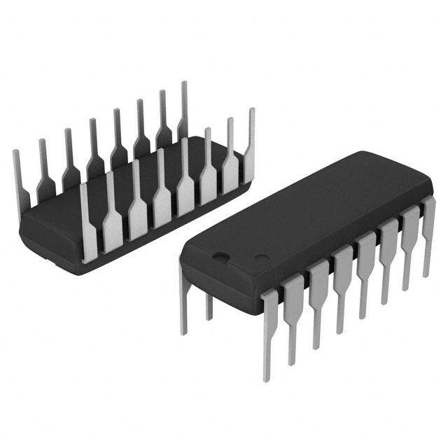
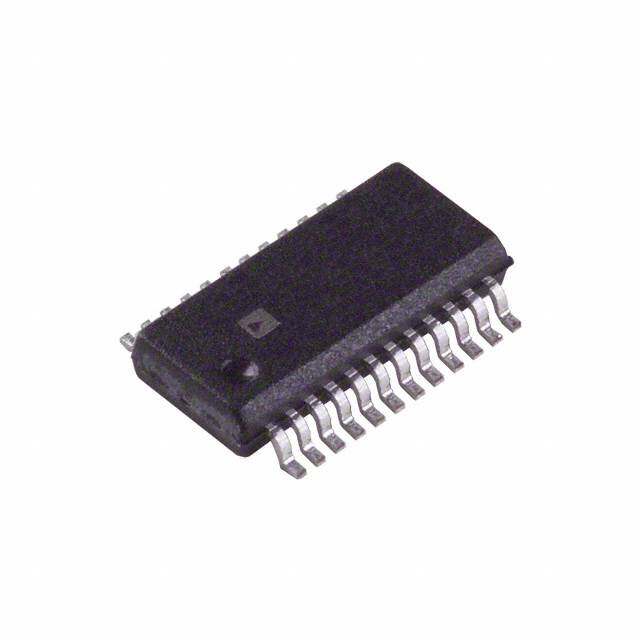
| 供应商器件封装 | 8-SOIC |
| 其它名称 | LT1249IS8PBF |
| 包装 | 管件 |
| 安装类型 | 表面贴装 |
| 封装/外壳 | 8-SOIC(0.154",3.90mm 宽) |
| 工作温度 | -40°C ~ 125°C |
| 标准包装 | 100 |
| 模式 | 平均电流 |
| 电压-电源 | 15.5 V ~ 27 V |
| 电流-启动 | 250µA |
| 频率-开关 | 100kHz |


- 商务部:美国ITC正式对集成电路等产品启动337调查
- 曝三星4nm工艺存在良率问题 高通将骁龙8 Gen1或转产台积电
- 太阳诱电将投资9.5亿元在常州建新厂生产MLCC 预计2023年完工
- 英特尔发布欧洲新工厂建设计划 深化IDM 2.0 战略
- 台积电先进制程称霸业界 有大客户加持明年业绩稳了
- 达到5530亿美元!SIA预计今年全球半导体销售额将创下新高
- 英特尔拟将自动驾驶子公司Mobileye上市 估值或超500亿美元
- 三星加码芯片和SET,合并消费电子和移动部门,撤换高东真等 CEO
- 三星电子宣布重大人事变动 还合并消费电子和移动部门
- 海关总署:前11个月进口集成电路产品价值2.52万亿元 增长14.8%


PDF Datasheet 数据手册内容提取
LT1249 Power Factor Controller FEATURES DESCRIPTIOU n Standard 8-Pin Packages The 8-pin LT®1249 provides active power factor correc- n High Power Factor Over Wide Load Range tion for universal offline power systems with very few with Line Current Averaging external parts. By using fixed high frequency PWM current n International Operation Without Switches averaging without the need for slope compensation, the n Instantaneous Overvoltage Protection LT1249 achieves far lower line current distortion, with a n Minimal Line Current Dead Zone smaller magnetic element than systems that use either peak n Typical 250m A Start-Up Supply Current current detection or zero current switching approach, in n Rejects Line Switching Noise both continuous and discontinuous modes of operation. n Synchronization Capability The LT1249 uses a multiplier containing a square gain n Low Quiescent Current: 9mA function from the voltage amplifier to reduce the AC gain n Fast 1.5A Peak Current Gate Driver at light output load and thus maintains low line current distortion and high system stability. The LT1249 also APPLICATIOU S provides filtering capability to reject line switching noise which can cause instability when fed into the multiplier. n Universal Power Factor Corrected Power Supplies n Preregulators up to 1500W at the current input to the multiplier. The LT1249 provides many protection features including peak current limiting and overvoltage protection. The switching frequency is internally set at 100kHz. While the LT1249 simplifies PFC design with minimal parts count, the LT1248 provides flexibilities in switching frequency, overvoltage and current limit. , LTC and LT are registered trademarks of Linear Technology Corporation. BLOCK DIAGRAW VAOUT MOUT CAOUT GND VCC 5 3 2 1 7.5V 7 VREF VSENSE 72.25mmVAA44 +EA R4kMOUT VCC + RUN 6 – IA MULTIPLIER IM 250m A MAX 16V/10V – IA4C IB 32k IM = 2I0A02m IBA2 +CA – – R Q + GTDR 15m A S gm = 1/3k + RUN 8 1V + 0.7V M1 – + SYNC OSC 4k – 16V 20m A 35pF 1249 BD 1
LT1249 ABSOLUTE WMAXIWMUWM RATINUGS PACKAGE/ORDER IUNFORWMATIOUN Supply Voltage ....................................................... 27V ORDER PART GTDR Current Continuous..................................... 0.5A TOP VIEW NUMBER GTDR Output Energy (Per Cycle)............................. 5m J GND 1 8 GTDR I Input Current ................................................. 20mA LT1249CN8 AC V Input Voltage ............................................ V CAOUT 2 7 VCC LT1249IN8 SENSE MAX M Input Current.............................................. – 5mA MOUT 3 6 VSENSE LT1249CS8 OUT IAC 4 5 VAOUT LT1249IS8 Operating Junction Temperature Range LT1249C................................................0(cid:176) C to 100(cid:176) C N8 PACKAGE 8-LEAD PDIP S8 PART LT1249I........................................... –40(cid:176) C to 125(cid:176) C S8 PACKAGE MARKING 8-LEAD PLASTIC SO Thermal Resistance (Junction-to-Ambient) N8 Package ................................................ 100(cid:176) C/W TJMAX = 125(cid:176)C, q JA = 100(cid:176)C/W (N8) 1249 TJMAX = 125(cid:176)C, q JA = 120(cid:176)C/W (S8) S8 Package................................................. 120(cid:176) C/W 1249I Storage Temperature Range..................–65(cid:176) C to 150(cid:176) C Consult factory for Military grade parts. Lead Temperature (Soldering, 10 sec)................. 300(cid:176) C ELECTRICAL CHARACTERISTICS The l denotes specifications which apply over the operating temperature range, otherwise specifications are at T = 25(cid:176) C. Maximum operating voltage (V ) = 25V, V = 18V, I = 100m A, CA = 3.5V, A MAX CC AC OUT VA = 5V, no load on any outputs, unless otherwise noted. OUT PARAMETER CONDITIONS MIN TYP MAX UNITS Overall Supply Current (V in Undervoltage Lockout) V = Lockout Voltage – 0.2V l 0.25 0.45 mA CC CC Supply Current, On 11.5V £ V £ V , CA = 1V l 9 12 mA CC MAX OUT V Turn-On Threshold l 15.5 16.5 17.5 V CC V Turn-Off Threshold l 9.5 10.5 11.5 V CC Voltage Amplifier V Bias Current V = 0V to 7V l –25 –250 nA SENSE SENSE Voltage Amp Gain 70 100 dB Voltage Amp Unity-Gain Bandwidth 1.5 MHz Voltage Amp Output High 0 £ Source Current £ 50m A l 10 12 V Voltage Amp Output Low 0 £ Sink Current £ 5m A l 0.1 0.4 V Voltage Amp Source Current l 130 260 450 m A Voltage Amp Sink Current Threshold Linear Operation, 2V < VA < 10V l 33 44 57 m A OUT Voltage Amp Sink Current Hysteresis 2V < VA < 10V l 14 22.5 30 m A OUT Current Amplifier Current Amp Offset Voltage l – 2 – 15 mV Current Amp Transconductance D I = – 40m A l 150 320 550 m mho CAOUT Current Amp Voltage Gain 2.5V £ V £ 7.5V 500 1000 V/V CAOUT Current Amp Source Current V = 1V, I = 0m A 100 145 220 m A MOUT M Current Amp Sink Current V = –0.3V, I = 0m A 67 95 125 m A MOUT M Current Amp Output High 7.4 8.1 V Current Amp Output Low 1.2 2 V 2
LT1249 ELECTRICAL CHARACTERISTICS The l denotes specifications which apply over the operating temperature range, otherwise specifications are at T = 25(cid:176) C. Maximum operating voltage (V ) = 25V, V = 18V, I = 100m A, CA = 3.5V, A MAX CC AC OUT VA = 5V, no load on any outputs, unless otherwise noted. OUT PARAMETER CONDITIONS MIN TYP MAX UNITS Reference Reference Output Voltage T = 25(cid:176) C, Measured at V Pin 7.39 7.5 7.6 V A SENSE Reference Output Voltage Worst Case All Line, Temperature l 7.32 7.5 7.68 V Reference Output Voltage Line Regulation V < V < V l –20 5 20 mV LOCKOUT CC MAX Multiplier Multiplier Output Current I = 100m A, VA = 5V 35 m A AC OUT Multiplier Output Current Offset R = 1M from I to GND l –0.05 –0.5 m A AC AC Multiplier Max Output Current (I ) I = 450m A, VA = 7V (Note 2) l –375 –250 –150 m A M(MAX) AC OUT Multiplier Max Output Voltage (I • R ) I = 450m A, VA = 7V (Note 2) l –1.25 –1.1 –0.96 V M(MAX) MOUT AC OUT Multiplier Gain Constant (Note 3) 0.035 V–2 I Input Resistance I from 50m A to 1mA 15 32 50 kW AC AC Oscillator Oscillator Frequency l 75 100 125 kHz Control Pin (CA ) Threshold Duty Cycle = 0 l 1.3 1.8 2.3 V OUT Synchronization Frequency Range Synchronizing Pulse Low £ 0.35V on CA l 127 160 kHz OUT Gate Driver Max GTDR Output Voltage 0mA Load, 18V < V < V (Note 4) l 12 15 17.5 V CC MAX GTDR Output High –200mA Load, 11.5V £ V £ 15V l V – 3.0 V CC CC GTDR Output Low (Device Unpowered) V = 0V, 50mA Load (Sinking) l 0.9 1.5 V CC GTDR Output Low (Device Active) 200mA Load (Sinking) l 0.5 1 V Peak GTDR Current 10nF from GTDR to GND 1.5 A GTDR Rise and Fall Time 1nF from GTDR to GND 25 ns GTDR Max Duty Cycle 90 96 % I Note 1: Absolute Maximum Ratings are those values beyond which the life Note 3: Multiplier Gain Constant: K = M of a device may be impaired. IAC (VAOUT – 1.5)2 Note 2: Current amplifier is in linear mode with 0V input common mode. Note 4: Maximum GTDR output voltage is internally clamped for higher V voltages. CC TYPICAL PERFORWMANUCE CHARACTERISTICS Voltage Amplifier Open-Loop Transconductance of Gain and Phase Current Amplifier 100 0 400 20 q 350 0 80 –20 gm o) GAIN mh300 –20 GAIN (dB) 642000 PHASE –––468000PHASE (DEG) mSCONDUCTANCE (221505000 –––486000PHASE (DEG) AN100 –100 R 0 –100 T 50 –120 –20 –120 0 –140 10 100 1k 10k 100k 1M 10M 1k 10k 100k 1M 10M FREQUENCY (Hz) FREQUENCY (Hz) 1249 G01 1249 G02 3
LT1249 TYPICAL PERFORWMANUCE CHARACTERISTICS Reference Voltage vs Temperature Multiplier Current 7.536 300 7.524 VAOUT = 6.5V VAOUT = 5V 7.512 V) VAOUT = 6V AGE (7.500 VAOUT = 5.5V VAOUT = 4.5V T OL7.488 A) NCE V7.476 mI (M150 VAOUT = 4V E R7.464 EFE VAOUT = 3.5V R7.452 VAOUT = 3V 7.440 VAOUT = 2.5V 7.428 0 VAOUT = 2V –75 –50 –25 0 25 50 75 100 125 150 0 250 500 JUNCTION TEMPERATURE (°C) IAC (m A) 1249 G03 1249 G04 Supply Current vs Supply Voltage GTDR Source Current GTDR Sink Current 10 18.5 1.1 9 TJ = –55°C 18.0 VCC = 18V 1.0 8 TJ = 25°C 17.5 0.9 Y CURRENT (mA) 7654 TJ = 125°C R VOLTAGE (V)11117665....0505 TJ = 125°C R VOLTAGE (V) 0000....8765 TA = –55°C SUPPL 32 GTD111544...050 TTJJ = = – 2555°°CC GTD 000...432 TA = 25°C 1 13.5 0.1 TA = 125°C 0 13.0 0 10 12 14 16 18 20 22 24 26 28 30 0 –60 –120 –180 –240 –300 0 60 120 180 240 300 SUPPLY VOLTAGE (V) SOURCE CURRENT (mA) SINK CURRENT (mA) 1249 G05 1249 G06 1249 G07 Start-Up Supply Current vs GTDR Rise and Fall Time Supply Voltage Switching Frequency 400 550 140 500 130 450 300 A) 400 120 mT ( 350 Hz) TIME (ns)200 FALL TIME Y CURREN 320500 –5255°°CC QUENCY (k 111000 RISE TIME PL 200 125°C RE 100 SUP 150 F 90 100 NOTE: GTDR SLEWS 80 BETWEEN 1V AND 16V 50 0 0 70 0 10 20 30 40 50 0 2 4 6 8 10 12 14 16 18 20 –75 –50 –25 0 25 50 75 100 125 LOAD CAPACITANCE (nF) SUPPLY VOLTAGE (V) TEMPERATURE (°C) 1249 G08 1249 G09 1249 G10 4
LT1249 TYPICAL PERFORWMANUCE CHARACTERISTICS Synchronization Threshold Transconductance of Current at CA M Pin Characteristics Amplifier Over Temperature OUT OUT 1.0 1.2 400 125°C 0.9 1.0 V) 25°C 350 HRONIZATION THRESHOLD ( 000000......876543 M CURRENT (mA)OUT––000000......8642024 –50°C mANSCONDUCTANCE (mho) 322110505000000 C 0.2 R N –0.6 T SY 0.1 –0.8 50 0 –1.0 0 –50 –25 0 25 50 75 100 125 –2.4 –1.2 0 1.2 2.4 –50 –25 0 25 50 75 100 125 TEMPERATURE (°C) MOUT VOLTAGE (V) TEMPERATURE (°C) 1249 G11 1249 G12 1249 G13 Voltage Amp Sink Current Limits Maximum Multiplier Output (Threshold) Voltage (I • R ) Maximum Duty Cycle M(MAX) MOUT 60 –1.30 100 99 –1.25 50 98 UP THRESHOLD –1.20 mCURRENT (A) 432000 DOWN THRESHOLD · R (V)M(MAX)MOUT–––111...110505 DUTY CYCLE (%) 9999976543 I –1.00 92 10 –0.95 91 0 –0.90 90 –75 –50 –25 0 25 50 75 100 125 –75 –50 –25 0 25 50 75 100 125 –50 –25 0 25 50 75 100 125 TEMPERATURE (°C) TEMPERATURE (°C) TEMPERATURE (°C) NOTE: THESE SINK CURRENT THRESHOLDS ARE 1249 G15 1249 G16 FOR OVERVOLTAGE PROTECTION FUNCTION. 1249 G14 PIUN FUUNCTIOUNS GND (Pin 1): Ground. is normally at negative potential and only AC signals appear at the noninverting input of the current amplifier. CA (Pin 2): This is the output of the current amplifier OUT that senses and forces the line current to follow the I (Pin 4): This is the AC line voltage sensing input to the AC reference signal that comes from the multiplier by com- multiplier. It is a current input that is biased at 2V to manding the pulse width modulator. When CA is low, minimize the crossover dead zone caused by low line OUT the modulator has zero duty cycle. voltage. A 32k resistor is in series with the current input, so that a small external capacitor can be used to filter out M (Pin 3): The multiplier current goes out of this pin OUT the switching noise from the high impedance lines. through the 4k resistor R . The voltage developed MOUT across R is the reference voltage of the current loop VA (Pin 5): This is the output of the voltage error MOUT OUT and it is limited to 1.1V. The noninverting input of the amplifier. The output is clamped at 12V. When the output current amplifier is also tied to R . In operation, M goes below 1.5V, the multiplier output current is zero. MOUT OUT 5
LT1249 PIUN FUUNCTIOUNS V (Pin 6): This is the inverting input to the voltage capacitor in parallel with a low ESR electrolytic capacitor, SENSE amplifier. 56m F or higher is required in close proximity to IC GND. V (Pin 7): This is the supply of the chip. The LT1249 has GTDR (Pin 8): The MOSFET gate driver is a 1.5A fast totem CC a very fast gate driver required to fast charge high power pole output. It is clamped at 15V. Capacitive loads like MOSFET gate capacitance. High current spikes occur MOSFET gates may cause overshoot. A gate series resis- during charging. For good supply bypass, a 0.1m F ceramic tor of at least 5W will prevent the overshoot. APPLICATIOUNS INUFORWMATIOUN Error Amplifier Multiplier The error amplifier has a 100dB DC gain and 1.5MHz unity- The multiplier is a current multiplier with high noise gain frequency. It is internally clamped at 12V. The nonin- immunity in a high power switching environment. The verting input is tied to the 7.5V reference. current gain is: I = (I )(I 2)/(200m A)2, and Current Amplifier M AC EA I = (VA – 1.5V)/25k EA OUT The multiplier output current I flows out of the M pin M OUT With a square function, because of the lower gain at light through the 4k resistor R and develops the reference MOUT power load, system stability is maintained and line current signal to the current loop that is controlled by the current distortion caused by the AC ripple fed back to the error amplifier. Current gain is the ratio of R to line current MOUT amplifier is minimized. Note that switching ripple on the sense resistor. The current amplifier is a transconductance high impedance lines could get into the multiplier from the amplifier. Typical g is 320m mho and gain is 60dB with no m I pin and cause instability. The LT1249 provides an load. The inverting input is internally tied to GND. The AC internal 25k resistor in series with the low impedance noninverting input is tied to the multiplier output. The multiplier current input so that only a capacitor from the output is internally clamped at 8V. Output resistance is I pin to GND is needed to filter out the noise. Maximum about 4M; DC loading should be avoided because it will AC multiplier output current is limited to 250m A. Figure 1 lower the gain and introduce offset voltage at the inputs shows the multiplier transfer curves. which becomes a false reference signal to the current loop and can distort line current. Note that in the current 300 averaging operation, high gain at twice the line frequency is necessary to minimize line current distortion. Because VAOUT = 6.5V VAOUT = 5V CAOUT may need to swing 5V over one line cycle at high line VAOUT = 6V condition, 11mV will be present at the inputs of the current VAOUT = 5.5V VAOUT = 4.5V amplifier if gain is rolled off to 450 at 120Hz (1nF in series A) with 10k at CA ). At light load, when (I )(R ) can be m (M150 VAOUT = 4V OUT M MOUT I less than 100mV, lower gain will distort the current loop VAOUT = 3.5V reference signal and line current. If signal gain at the VAOUT = 3V 100kHz switching frequency is too high, the system VAOUT = 2.5V behaves more like a current mode system and can cause 0 VAOUT = 2V 0 250 500 subharmonic oscillation. Therefore, the current amplifier IAC (m A) should be compensated to have a gain of less than 15 at 1249 G04 100kHz and more than 300 at 120Hz. Figure 1. Multiplier Current I vs I and VA M AC OUT 6
LT1249 APPLICATIOUNS INUFORWMATIOUN Line Current Limiting With ts = 30ns, fs = 130kHz, V = 3V and R2 = 10k, offset C voltage shift is » 5mV. Note that this offset voltage will add Maximum voltage across R is internally limited to MOUT slight distortion to line current at light load. 1.1V. Therefore, line current limit is 1.1V divided by the sense resistor R . With a 0.2W sense resistor R line S S current limit is 5.5A. As a general rule, RS is chosen CAOUT VCC according R1 1N5712 10k (I )(R )(V ) 80pF RS = M(MKAX(1).41M4)OPUT LINE(MIN) R102k 2N2369 50VV OUT(MAX) 1nF 2k where POUT(MAX) is the maximum power output and K is 1249 F02 usually between 1.1 and 1.3 depending on efficiency and resistor tolerance. When the output is overloaded and line Figure 2. Synchronizing the LT1249 current reaches limit, output voltage V will drop to keep OUT line current constant. System stability is still maintained Overvoltage Protection by the current loop which is controlled by the current In Figure 3, R1 and R2 set the regulator output DC level: amplifier. Further load current increase results in further V = V [(R1 + R2)/R2]. With R1 = 1M and R2 = 20k, V drop and clipping of the line current, which degrades OUT REF OUT V is 382V. power factor. OUT Because of the slow loop response necessary for power Synchronization factor correction, output overshoot can occur with sudden load removal or reduction. To protect the power compo- The LT1249 can be externally synchronized in a frequency nents and output load, the LT1249 voltage error amplifier range of 127kHz to 160kHz. Figure 2 shows the synchro- senses the output voltage and quickly shuts off the current nizing circuit. Synchronizing occurs when CA pin is OUT switch when overvoltage occurs. When overshoot occurs pulled below 0.5V with an external transistor and a Schottky on V , the overcurrent from R1 will go through VA diode. The Schottky diode and the 10k pull-up resistor are OUT OUT because amplifier feedback keeps V locked at 7.5V. necessary for the required fast slewing back up to the SENSE When this overcurrent reaches 44m A amplifier sinking normal operating voltage on CA after the transistor is OUT limit, the amplifier loses feedback and its output snaps low turned off. Positive slewing on CA should be faster OUT than the oscillator ramp rate of 0.5V/m s. to turn the multiplier off. Overvoltage trip level: D V = (44m A)(R1) The width of the synchronizing pulse should be under OUT 60ns. The synchronizing pulses introduce an offset volt- 0.047m F age on the current amplifier inputs, according to: VOUT (ts)(fs)(cid:230)(cid:231) IC+ VC- 0.5(cid:246)(cid:247) 0.4C71m F 3R303k Ł R2 ł D V = OS R1 g m 1M VSENSE – VAOUT ts = pulse width EA fs = pulse frequency R2 + 44m A 20k IC = CAOUT source current (» 150m A) VREF MULTIPLIER 22m A 7.5V V = CA operating voltage (1.8V to 6.8V) C OUT LT1249 R2 = resistor for the midfrequency “zero” in the current loop 1249 F03 gm = current amplifier transconductance (» 320m mho) Figure 3. Overvoltage Protection 7
LT1249 APPLICATIOUNS INUFORWMATIOUN The Figure 3 circuit therefore has 382V on V , and an LINE MAIN INDUCTOR OUT overvoltage level = (V + 44V), or 426V. With a 22m A NP R1 OUT NS 90k hysteresis, V then has to drop 22V to 404V before 1W OUT feedback recovers and the switch turns back on. D1 D3 + VCC MOUT is a high impedance current output. In the current C1 2m F + + loop, offset line current is determined by multiplier offset D2 C3 C4 + 390m F 56m F current and input offset voltage of the current amplifier. C2 2m F A negative 4mV current amplifier V translates into OS 20mA line current and 5W input power for 250V line if ALL CAPACITORS ARE RATED 35V 1249 F04 0.2W sense resistor is used. Under no load or when the Figure 4. Power Supply for LT1249 load power is less than this offset input power, V would OUT slowly charge up to an overvoltage state because the overvoltage comparator can only reduce multiplier output C2 current to zero. This does not guarantee zero output 1000pF MAIN INDUCTOR LINE current if the current amplifier has offset. To regulate V 450V OUT under this condition, the amplifier M1 (see Block Dia- R1 gram), becomes active in the current loop when VAOUT D2 D3 910Wk goes down to 1V. The M1 can put out up to 15m A to the 4k + C3 + C4 VCC resistor at the inverting input to cancel the current ampli- D1 390m F 18V 56m F 35V 35V fier negative V and keep V error to within 2V. OS OUT 1249 F05 Undervoltage Lockout Figure 5. Power Supply for LT1249 The LT1249 turns on when V is higher than 16V and CC remains on until V falls below 10V, whereupon the chip CC auxiliary winding determines V according to: V /(V CC OUT CC enters the lockout state. In the lockout state, the LT1249 – 2V) = N /N . For 382V V and 18V V , N /N » 19. P S OUT CC P S only draws 250m A, the oscillator is off, the V and the REF In Figure 5 a new technique for supply voltage eliminates GTDR pins remain low to keep the power MOSFET off. the need for an extra inductor winding. It uses capacitor Start-Up and Supply Voltage charge transfer to generate a constant current source which feeds a Zener diode. Current to the Zener is equal to The LT1249 draws only 250m A before the chip starts at (V – V )(C)(f), where V is Zener voltage and f is OUT Z Z 16V on V . To trickle start, a 90k resistor from the power CC switching frequency. For V = 382V, V = 18V, C = OUT Z line to V supplies the trickle current and C4 holds the V CC CC 1000pF and f = 100kHz, Zener current will be 36mA. This up while switching starts (see Figure 4). Then the auxiliary is enough to operate the LT1249, including the FET gate winding takes over and supplies the operating current. drive. Note that D3 and the large value C3, in both Figures 4 and 5, are only necessary for systems that have sudden large Output Capacitor load variation down to minimum load and/or very light The peak-to-peak 120Hz output ripple is determined by: load conditions. Under these conditions, the loop may exhibit a start/restart mode because switching remains off V = (2)(I DC)(Z) P-P LOAD long enough for C4 to discharge below 10V. The C3 will where I DC: DC load current hold V up until switching resumes. For less severe load LOAD CC Z: capacitor impedance at 120Hz variations, D3 is replaced with a short and C3 is omitted. The turns ratio between the primary winding and the For 180m F at 300W load, I DC = 300W/385V = 0.78A, LOAD 8
LT1249 APPLICATIOUNS INUFORWMATIOUN V = (2)(0.78A)(7.4W ) = 11.5V. If less ripple is desired, The 120Hz ripple current rating at 105(cid:176) C ambient is 0.95A P-P higher capacitance should be used. for the 180m F KMH 400V capacitor. The expected life of the output capacitor may be calculated from the thermal The selection of the output capacitor should also be based stress analysis: on the operating ripple current through the capacitor. The ripple current can be divided into three major compo- (105(cid:176) C+ D TK)–(TAMB+D TO) L=(L )(2) nents. The first is at 120Hz whose RMS value is related to O 10 the DC load current as follows: where I » (0.71)(I DC) 1RMS LOAD L = expected life time The second component contains the PF switching fre- L = hours of load life at rated ripple current and rated O quency ripple current and its harmonics. Analysis of this ambient temperature ripple is complicated because it is modulated with a 120Hz D T = capacitor internal temperature rise at rated condi- signal. However, computer numerical integration and Fou- K tion. D T = (I2R)/(KA), where I is the rated current, R is rier analysis approximate the RMS value reasonably close K capacitor ESR, and KA is a volume constant. to the bench measurements. The RMS value is about 0.82A at a typical condition of 120VAC, 200W load. This T = operating ambient temperature AMB ripple is line voltage dependent, and the worst case is at D T = capacitor internal temperature rise at operating O low line. condition I2RMS = 0.82A at 120VAC, 200W In our example, LO = 2000 hours and D TK = 10(cid:176) C at rated The third component is the switching ripple from the load, 0.95A. D TO can then be calculated from: if the load is a switching regulator. 2 2 (cid:230) I (cid:246) (cid:230) 0.77A(cid:246) I3RMS » ILOADDC D TO =Ł(cid:231) 0R.9M5SAł(cid:247) D ( TK)=Ł(cid:231) 0.95Ał(cid:247) (10(cid:176) C)= 6.6(cid:176) C For United Chemicon KMH 400V capacitor series, ripple Assuming the operating ambient temperature is 60(cid:176) C, the current multiplier for currents at 100kHz is 1.43. The approximate life time is: equivalent 120Hz ripple current can then be found: (105(cid:176) C+ 10(cid:176) C)–(6(cid:176)0+C 6(cid:176) .6 C) L » (2000)(2) ( ) (cid:230) (cid:246) 2 (cid:230) (cid:246) 2 O 10 2 I I I = I +(cid:231) 2RMS(cid:247) +(cid:231) 3RMS(cid:247) » 57,000 Hrs. RMS 1RMS Ł 1.43ł Ł 1.43ł For longer life, capacitor with higher ripple current rating For a typical system that runs at an average load of 200W or parallel capacitors should be used. and 385V output: Protection Against Abnormal Current Surge I DC = 0.52A Conditions LOAD I » (0.71)(0.52A) = 0.37A 1RMS The LT1249 has an upper limit on the allowed voltage I » 0.82A at 120VAC 2RMS across the current sense resistor. The voltage into the I » I DC = 0.52A M pin connected to this resistor must not exceed –6V 3RMS LOAD OUT while the chip is running and –12V under any conditions. ( )2 (cid:230) 0.82A(cid:246) 2 (cid:230) 0.52A(cid:246) 2 The LT1249 gate drive will malfunction if the MOUT pin I = 0.37A +(cid:231) (cid:247) +(cid:231) (cid:247) = 0.77A voltage exceeds –6V while VCC is powered, destroying the RMS Ł 1.43 ł Ł 1.43 ł power FET. The 12V absolute limit is imposed by ESD clamps on the M pin. Large currents will flow at OUT 9
LT1249 APPLICATIOUNS INUFORWMATIOUN voltages above 8V and the 12V limit is only for surge resistor, the standard LT1249 application will not be conditions. affected because the chip is not yet powered. Problems are only created if the V pin is powered from some external In normal operation, the voltage into M does not CC OUT housekeeping supply that remains powered when bridge exceed 1.1V, but under surge conditions, the voltage power is switched off. could temporarily go higher. To date, no field failures due to surges have been reported for normal LT1249 configu- A huge line voltage surge, beyond the normal worst-case rations, but if the possibility exists for extremely large limits, can also create a large current surge. The peak of current surges, please read the following discussion. the line voltage must significantly exceed the storage capacitor voltage (typically 380V) for this to occur, so peak Offline switching power supplies can create large current line voltage would probably have to exceed 450V. Such surges because of the high value storage capacitor used. excessive surges might occur if a very large mains load The surge can be the result of closing the line switch near was suddenly removed, with a resulting line “kickback”. If the peak of the AC line voltage, or because of a large the surge results in voltage at the M pin greater than transient in the line itself. These surges are well known in OUT 6V, it must also last more than 30m s (three switch cycles) the power supply business, and are normally controlled to cause FET problems. with a negative temperature coefficient thermistor in series with the rectifier bridge. When power is switched External Clamp on, the thermistor is cold (high resistance) and surges are limited. Current flow in the thermistor causes it to heat and The external clamp shown in Figure 6 will protect the resistance drops to the point where overall efficiency loss LT1249 M pin against extremely large line current OUT in the resistor is acceptable. surges (see above). Protection is provided for all V CC power methods. The 100W resistor and three diodes limit This basic protection mechanism can be partially defeated the peak negative voltage into M to less than 3V. if the power supply is switched off for a few seconds, then OUT Current sense gain is attenuated by only 100W /4000W = turned back on. The thermistor has not had time to cool 2.5%. Three diodes are used because the peak negative significantly and if the subsequent turn-on catches the AC voltage into M in normal operation could go as high as line near its peak, the resulting surge is much higher than OUT –1.1V and the diodes should not conduct more than a few normal. Even if this surge current generates a voltage microamps under this condition. greater than 6V (but less than 12V) across the sense THERMISTOR + + BRIDGE SURGE PATH STORAGE CAPACITOR – RS 100Ω MOUT LT1249 Figure 6. Protecting M from Extremely High Current Surges OUT 10
LT1249 PACKAGE DESCRIPTIOUN Dimensions in inches (millimeters) unless otherwise noted. N8 Package 8-Lead PDIP (Narrow 0.300) (LTC DWG # 05-08-1510) 0.400* (10.160) MAX 8 7 6 5 0.255 – 0.015* (6.477 – 0.381) 1 2 3 4 0.300 – 0.325 0.045 – 0.065 0.130 – 0.005 (7.620 – 8.255) (1.143 – 1.651) (3.302 – 0.127) 0.065 (1.651) 0.009 – 0.015 TYP (0.229 – 0.381) 0.125 (3.175) 0.020 (0.325–+00..003155) 0.100 0.018 – 0M.0I0N3 (0M.5I0N8) 8.255+0.889 (2.54) (0.457 – 0.076) –0.381 BSC N8 1098 *THESE DIMENSIONS DO NOT INCLUDE MOLD FLASH OR PROTRUSIONS. MOLD FLASH OR PROTRUSIONS SHALL NOT EXCEED 0.010 INCH (0.254mm) S8 Package 8-Lead Plastic Small Outline (Narrow 0.150) (LTC DWG # 05-08-1610) 0.189 – 0.197* (4.801 – 5.004) 8 7 6 5 0.228 – 0.244 0.150 – 0.157** (5.791 – 6.197) (3.810 – 3.988) 1 2 3 4 0.010 – 0.020 · 45(cid:176) 0.053 – 0.069 (0.254 – 0.508) (1.346 – 1.752) 0.004 – 0.010 0.008 – 0.010 (0.203 – 0.254) 0°– 8° TYP (0.101 – 0.254) 0.016 – 0.050 0.014 – 0.019 0.050 (0.406 – 1.270) (0.355 – 0.483) (1.270) TYP BSC *DIMENSION DOES NOT INCLUDE MOLD FLASH. MOLD FLASH SHALL NOT EXCEED 0.006" (0.152mm) PER SIDE **DIMENSION DOES NOT INCLUDE INTERLEAD FLASH. INTERLEAD FLASH SHALL NOT EXCEED 0.010" (0.254mm) PER SIDE SO8 1298 Information furnished by Linear Technology Corporation is believed to be accurate and reliable. 11 However, no responsibility is assumed for its use. Linear Technology Corporation makes no represen- tation that the interconnection of its circuits as described herein will not infringe on existing patent rights.
LT1249 TYPICAL APPLICATIONU 750m H* MURH860 + VOUT 90V EMI TO FILTER 270V 6A – + IRF840 1M 180m F 0.047m F RS 20k 0.2W 0.47m F 330k 1nF 100pF 10W 10k † VAOUT MOUT CAOUT GND VCC 5 3 2 1 7 7.5V 7.5V + R4kMOUT VREF EA 6 – MAX VCC + RUN 1M 4VSENSE IIBA MIMU =L T2II0AP02Lm IIBAER2 IM 25+0CmAA 16V/10V –– – R Q IAC 32k 15m A gm = 1/3k 0.7V + + RUN S 8 GTDR 1V + – M1 – + SYNC OSC 4.7nF 4242mm AA 4k – 20m A 16V 1N58*1*9 35pF * 1. COILTRONICS CTX02-12236 (TYPE 52 CORE) 1249 TA01 AIR MOVEMENT NEEDED AT POWER LEVEL GREATER THAN 250W. 2. COILTRONICS CTX02-12295 (MAGNETICS Kool Mm ® 77930 CORE) ** THIS SCHOTTKY DIODE IS TO CLAMP GTDR WHEN MOS SWITCH TURNS OFF. PARASITIC INDUCTANCE AND GATE CAPACITANCE MAY TURN ON CHIP SUBSTRATE DIODE AND CAUSE ERRATIC OPERATIONS IF GTDR IS NOT CLAMPED. † SEE APPLICATIONS INFORMATION SECTION FOR CIRCUITRY TO SUPPLY POWER TO VCC. RELATED PARTS PART NUMBER DESCRIPTION COMMENTS LT1103 Off-Line Switching Regulator Universal Off-Line Inputs with Outputs to 100W LT1248 Full Feature Average Current Mode Power Factor Controller Provides All Features in 16-Lead Package LT1508 Power Factor and PWM Controller Simplified PFC Design LT1509 Power Factor and PWM Controller Complete Solution for Universal Off-Line Switching Power Supplies Kool Mm is a registered trademark of Magnetics, Inc. 12 Linear Technology Corporation sn1249 1249fbs LT/TP 0799 2K REV B • PRINTED IN USA 1630 McCarthy Blvd., Milpitas, CA 95035-7417 (408) 432-1900 l FAX: (408) 434-0507 l w ww.linear-tech.com ª LINEAR TECHNOLOGY CORPORATION 1994