ICGOO在线商城 > 集成电路(IC) > PMIC - PFC(功率因数修正) > UC2854BN
 Datasheet下载
- 型号: UC2854BN
- 制造商: Texas Instruments
- 库位|库存: xxxx|xxxx
- 要求:
| 数量阶梯 | 香港交货 | 国内含税 |
| +xxxx | $xxxx | ¥xxxx |
查看当月历史价格
查看今年历史价格
UC2854BN产品简介:
ICGOO电子元器件商城为您提供UC2854BN由Texas Instruments设计生产,在icgoo商城现货销售,并且可以通过原厂、代理商等渠道进行代购。 UC2854BN价格参考¥31.64-¥39.55。Texas InstrumentsUC2854BN封装/规格:PMIC - PFC(功率因数修正), PFC IC Average Current 80kHz ~ 120kHz 16-PDIP。您可以下载UC2854BN参考资料、Datasheet数据手册功能说明书,资料中有UC2854BN 详细功能的应用电路图电压和使用方法及教程。
UC2854BN是德州仪器(Texas Instruments)推出的一款用于功率因数校正(PFC)的控制器芯片,属于PMIC - PFC类别。其主要应用场景包括:

1. 工业电源:UC2854BN广泛应用于工业设备中的开关电源设计,例如不间断电源(UPS)、电机驱动器和工业自动化设备。它能够有效提高功率因数,减少谐波失真,从而满足严格的工业标准。

2. 消费电子:在高功率消费电子产品中(如大屏幕电视、家用空调和洗衣机等),UC2854BN可用于实现高效的功率因数校正,以满足能效法规要求并提升产品性能。

3. 通信设备:该芯片适用于通信基站、服务器电源和其他高可靠性电源系统。通过优化功率转换效率,UC2854BN可帮助降低能耗并延长设备寿命。

4. 照明系统:在LED路灯或高亮度商业照明应用中,UC2854BN可以确保稳定的电流输出和高功率因数,同时减少电网污染。

5. 太阳能逆变器:作为太阳能发电系统的一部分,UC2854BN有助于提高逆变器的整体效率,确保能量传输更加高效且符合电网接入标准。

总之,UC2854BN凭借其高性能和灵活性,成为众多需要高功率因数校正场合的理想选择,特别适合对效率和稳定性有严格要求的应用环境。
| 参数 | 数值 |
| 产品目录 | 集成电路 (IC)半导体 |
| 描述 | IC PFC CTRLR AVERAGE CURR 16DIP功率因数校正 - PFC Enhanced High Power Factor Preregulator |
| 产品分类 | |
| 品牌 | Texas Instruments |
| 产品手册 | |
| 产品图片 |
|
| rohs | 符合RoHS无铅 / 符合限制有害物质指令(RoHS)规范要求 |
| 产品系列 | 电源管理 IC,功率因数校正 - PFC,Texas Instruments UC2854BN- |
| 数据手册 | |
| 产品型号 | UC2854BN |
| 产品目录页面 | |
| 产品种类 | 功率因数校正 - PFC |
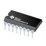
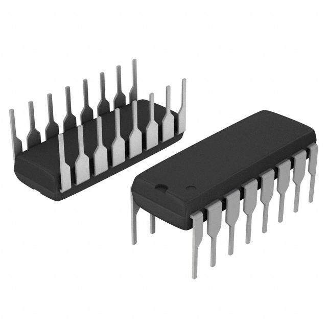
| 供应商器件封装 | 16-PDIP |
| 其它名称 | 296-11194-5 |
| 包装 | 管件 |
| 单位重量 | 1.054 g |
| 商标 | Texas Instruments |
| 安装类型 | 通孔 |
| 安装风格 | Through Hole |
| 封装 | Tube |
| 封装/外壳 | 16-DIP(0.300",7.62mm) |
| 封装/箱体 | PDIP-16 |
| 工作温度 | -40°C ~ 85°C |
| 工厂包装数量 | 25 |
| 开关频率 | 115 kHz |
| 最大工作温度 | + 85 C |
| 最小工作温度 | - 40 C |
| 标准包装 | 25 |
| 模式 | 平均电流 |
| 电压-电源 | 10 V ~ 20 V |
| 电流-启动 | 250µA |
| 系列 | UC2854B |
| 频率-开关 | 80kHz ~ 120kHz |


- 商务部:美国ITC正式对集成电路等产品启动337调查
- 曝三星4nm工艺存在良率问题 高通将骁龙8 Gen1或转产台积电
- 太阳诱电将投资9.5亿元在常州建新厂生产MLCC 预计2023年完工
- 英特尔发布欧洲新工厂建设计划 深化IDM 2.0 战略
- 台积电先进制程称霸业界 有大客户加持明年业绩稳了
- 达到5530亿美元!SIA预计今年全球半导体销售额将创下新高
- 英特尔拟将自动驾驶子公司Mobileye上市 估值或超500亿美元
- 三星加码芯片和SET,合并消费电子和移动部门,撤换高东真等 CEO
- 三星电子宣布重大人事变动 还合并消费电子和移动部门
- 海关总署:前11个月进口集成电路产品价值2.52万亿元 增长14.8%


PDF Datasheet 数据手册内容提取
UC1854A UC2854A, UC2854B UC3854A, UC3854B www.ti.com SLUS329E–MONTH2003–REVISEDJANUARY2008 ADVANCED HIGH-POWER FACTOR PREREGULATOR FEATURES 1 • ControlsBoostPWMtoNear-UnityPower DESCRIPTION Factor The UC3854A/B products are pin compatible • LimitsLineCurrentDistortionTo<3% enhanced versions of the UC3854. Like the UC3854, • World-WideOperationWithoutSwitches these products provide all of the functions necessary for active power factor corrected preregulators. The • AccuratePowerLimiting controller achieves near unity power factor by • Fixed-FrequencyAverageCurrent-Mode shaping the ac input line current waveform to Control correspond to the ac input line voltage. To do this the • HighBandwidth(5MHz),Low-OffsetCurrent UC3854A/B uses average current mode control. Average current mode control maintains stable, low Amplifier distortion sinusoidal line current without the need for • IntegratedCurrent-andVoltage-Amplifier slope compensation, unlike peak current mode OutputClamps control. • MultiplierImprovements:Linearity,500mVV AC A 1%, 7.5-V reference, fixed frequency oscillator, Offset(EliminatesExternalResistor),0Vto PWM, voltage amplifierwith soft-start, line voltage 5VMultoutCommon-ModeRange feedforward (V squarer), input supply voltage RMS • V GOODComparator clamp, and over current comparator round out the lilst REF • FasterandImprovedAccuracyENABLE offeataures. Comparator Available in the 16-pin N (PDIP), DW (SOIC Wide), • UVLOOptions(16V/10Vor10.5V/10V) and J (CDIP) and 20-pin Q (PLCC) package. See Ordering Information table for availability by • 300-m AStart-UpSupplyCurrent temperaturerange. BLOCK DIAGRAM VAO MOUT CAO PKLMT REF 7 5 3 2 9 VCC 7.5 V REF (A) 16 V / 10 V RUN (B) 10.5 V / 10 V ENA 10 IC 7.1 V 2.65 V / 2.15 V POWER 3 V 15 VCC A VSENSE 11 R IAC 6 B R 16 GTDRV S Q 8 X2 C VRMS 14 m A RUN 20 V SS 13 IMOUT(cid:2)A(cid:1)CB OSC 1 GND 4 14 12 ISENSE CT RSET 1 Pleasebeawarethatanimportantnoticeconcerningavailability,standardwarranty,anduseincriticalapplicationsof TexasInstrumentssemiconductorproductsanddisclaimerstheretoappearsattheendofthisdatasheet. PRODUCTIONDATAinformationiscurrentasofpublicationdate. Copyright©2003–2008,TexasInstrumentsIncorporated Products conform to specifications per the terms of the Texas Instruments standard warranty. Production processing does not necessarilyincludetestingofallparameters.
UC1854A UC2854A, UC2854B UC3854A, UC3854B www.ti.com SLUS329E–MONTH2003–REVISEDJANUARY2008 Thesedeviceshavelimitedbuilt-inESDprotection.Theleadsshouldbeshortedtogetherorthedeviceplacedinconductivefoam duringstorageorhandlingtopreventelectrostaticdamagetotheMOSgates. DESCRIPTION (CONTINUED) The UC3854A/B products improve upon the UC3854 by offering a wide bandwidth, low offset current amplifier, a faster responding and improved accuracy enable comparator, a VREF GOOD comparator, UVLO threshold options (16 V/10 V for offline, 10.5 V/10 V for startup from an auxiliary 12-V regulator), lower startup supply current,andanenhancedmultiply/dividecircuit.Newfeatures like the amplifier output clamps, improved amplifier current sinking capability, and low offset VAC pin reduce the external component count while improving performance. Improved common mode input range of the multiplier output/current amplifier input allow the designer greater flexibility in choosing amethod for current sensing. Unlike its predecessor, R controls only SET oscillator charging current and has no effect on clamping the maximum multiplier output current. This current is now clamped to a maximum of 2 · I at all times which simplifies the design process and provides foldback AC powerlimitingduringbrownoutandextremelowlineconditions. ORDERINGINFORMATION UVLO UVLO PARTNUMBERS TA TURN-ON TURN-OFF CDIP-16 PDIP-16 SOIC-16 PLCC-20 (V) (V) (V) (N) (DW) (Q) 16 10 – – – – –55(cid:176) Cto125(cid:176) C 10.5 10 UC1854BJ – – – 16 10 UC2854AJ UC2854AN UC2854ADW UC2854AQ –40(cid:176) Cto85(cid:176) C 10.5 10 UC2854BJ UC2854BN UC2854BDW UC2854BQ 16 10 – UC2854AN UC2854ADW – 0(cid:176) Cto70(cid:176) C 10.5 10 – UC2854BN UC2854BDW – ABSOLUTE MAXIMUM RATINGS overoperatingfree-airtemperaturerange(unlessotherwisenoted)(1) UCX854A,UCX854B UNIT V Supplyvoltage 22 V CC Continuous 0.5 I GTDRVcurrent A GTDRV 50%dutycycle 1.5 VSENSE,VRMS,ISENSEMOUT 11 Inputvoltage V PKLMT 5 Inputcurrent RSET,IAC,PKLMT,ENA 10 mA Powerdissipation 1 W T Junctiontemperature –55to150 J T Storagetemperature –65to150 (cid:176) C stg T Leadtemperataure,1,6mm(1/16inch)fromcasefor10seconds 300 sol (1) Stressesbeyondthoselistedunderabsolutemaximumratingsmaycausepermanentdamagetothedevice.Thesearestressratings only,andfunctionaloperationofthedeviceattheseoranyotherconditionsbeyondthoseindicatedunderrecommendedoperating conditionsisnotimplied.Exposuretoabsolute-maximum-ratedconditionsforextendedperiodsmayaffectdevicereliability.Allvoltages arewithrespecttoGND.Currentsarepositiveintoandnegativeoutof,thespecifiedterminal.ENAinputisinternallyclampedto approximately10V. 2 SubmitDocumentationFeedback Copyright©2003–2008,TexasInstrumentsIncorporated ProductFolderLink(s):UC1854AUC2854A,UC2854BUC3854A,UC3854B
UC1854A UC2854A, UC2854B UC3854A, UC3854B www.ti.com SLUS329E–MONTH2003–REVISEDJANUARY2008 RECOMMENDED OPERATING CONDITIONS overoperatingfree-airtemperaturerange(unlessotherwisenoted) MIN MAX UNIT V Supplyvoltage 10 20 V CC UC1854X –55 125 T Operatingjunctiontemperature UC2854X –40 85 (cid:176) C J UC3854X 0 70 THERMAL RESISTANCE PACKAGEDDEVICES RESISTANCES CDIP-16 PDIP-16 SOP-16 PLCC-20 (J) (N) (DW) (Q) q ((cid:176) C/W) 28(1) 45 27 34 JC q ((cid:176) C/W) 80–120 90(2) 50–130(2) 43–75(2) JA (1) q datavaluesstatedarederivedfromMIL-STD-1835Bwhichstatesgthebaselinevaluesshownareworstcase(mean+2s)fora60· JC 60milmicrocircuitdevicesilicondieandapplicablefordeviceswithdiesizesupto14,400squaremils.Fordevicediesizesgreaterthan 14,400squaremilsusethefollowingvalues,dual-in-line,11(cid:176) C/W;flatpackandpingridarray,10(cid:176) C/W.areattheendofeachtrace. (2) q (junction-to-ambient)appliestodevicesmountedtofivesquareinchFR4PCboardwithoneouncecopperwherenoted.When JA resitancerangeisgiven,lowervaluesareforfivesquareinchaluminumPCboard.TestPWBis0.062inchesthickandtypicallyuses 0,635mmtracewidthsforpowerpackagesand1,3mmtracewidthsfornon-powerpackageswitha100· 100milprobelandareatthe endofeachtrace. Copyright©2003–2008,TexasInstrumentsIncorporated SubmitDocumentationFeedback 3 ProductFolderLink(s):UC1854AUC2854A,UC2854BUC3854A,UC3854B
UC1854A UC2854A, UC2854B UC3854A, UC3854B www.ti.com SLUS329E–MONTH2003–REVISEDJANUARY2008 ELECTRICAL CHARACTERISTICS V =18V,R =8.2kΩ,C =1.5nF,V =1V,V =1.5V,I =100m A,I =0V,V =3.5V,V =5V, CC T T PKLMT VRMS IAC ISENSE CAO VAO V =3V,–40(cid:176) C<T <85(cid:176) CfortheUC2854AandUC2854B,and0(cid:176) C<T <70(cid:176) CfortheUC3854AandUC3854B, VSENSE A A andT =T (unlessotherwisenoted) A J PARAMETER TESTCONDITIONS MIN TYP MAX UNIT OVERALL CAO=0V, VAO=0V, Supplycurrent,off 250 400 m A V =V –0.3V CC UVLO Supplycurrent,on 12 18 mA UCx854A 15.0 16.0 17.5 V turn-onthresholdvoltage CC UCx854B 8.0 10.5 11.2 UCx854A 9 10 12 V turn-offthresholdvoltage CC UCx854B 7.8 10.3 11.0 V UCx854A 5 6 7 V hysteresis CC UCx854B 0.10 0.22 0.50 V clamp I =I +5mA 18 20 22 CC VCC VCC(on) VOLTAGEAMPLIFIER Inputvoltage 2.9 3.0 3.1 V V biascurrent –500 —25 500 nA SENSE Openloopgain 2V≤V ≤5V 70 100 dB OUT V High-leveloutputvoltage I =–500m A 6 OH LOAD V V Low-leveloutputvoltage I =500m A 0.3 0.5 OL LOAD I Outputshort-circuitcurrent V =0V 1.5 3.5 mA SC OUT Gainbandwidthproduct(1) f =100kHz, 10mVp-p 1 MHz IN CURRENTAMPLIFIER V =0V, T =25(cid:176) C –4 0 CM A Inputoffsetvoltage mV V =0V, Overtemperature –5.5 0 CM I Inputbiascurrent V =0V –500 500 nA SENSE CM Openloopgain 2V≤V =6V 80 110 dB OUT V High-leveloutputvoltage I =–500m A 8 OH LOAD V V Low-leveloutputvoltage I =500m A 0.3 0.5 OL LOAD I Outputshort-circuitcurrent V =0V 1.5 3.5 mA SC OUT CMRR Commonmoderejectionrange –0.3 5.0 V Gainbandwidthproduct(1) f =100kHz, 10mVp-p 3 5 MHz IN REFERENCE I =0mA, T =25(cid:176) C 7.4 7.5 7.6 REF A Outputvoltage V I =0mA 7.35 7.50 7.65 REF Loadregulation 1mA≤I ≤10mA 0 8 20 REF mV Lineregulation 12V≤V ≤18V 0 14 25 CC I Shortcircuitcurrent V =0V 25 35 60 mA SC REF (1) Ensuredbydesign.Notproductiontested. 4 SubmitDocumentationFeedback Copyright©2003–2008,TexasInstrumentsIncorporated ProductFolderLink(s):UC1854AUC2854A,UC2854BUC3854A,UC3854B
UC1854A UC2854A, UC2854B UC3854A, UC3854B www.ti.com SLUS329E–MONTH2003–REVISEDJANUARY2008 ELECTRICAL CHARACTERISTICS (Continued) V =18V,R =8.2kΩ,C =1.5nF,V =1V,V =1.5V,I =100m A,I =0V,V =3.5V,V =5V, CC T T PKLMT VRMS IAC ISENSE CAO VAO V =3V,–40(cid:176) C<T <85(cid:176) CfortheUC2854AandUC2854B,and0(cid:176) C<T <70(cid:176) CfortheUC3854AandUC3854B, VSENSE A A andT =T (unlessotherwisenoted) A J PARAMETER TESTCONDITIONS MIN TYP MAX UNIT OSCILLATOR Initialaccuracy T =25(cid:176) C 85 100 115 kHz A Voltagestability 12V≤V ≤18V 1% CC Totalvariation Line,temperature 80 120 kHz Rampamplitude(peak-to-peak) 4.9 5.9 V Rampvalleyvoltage 0.8 1.3 V ENABLE/SOFT-START/CURRENTLIMIT Enablethresholdvoltage 2.35 2.55 2.80 V Enaablehysteresis V =2.5V 500 600 mV FAULT Enableinputbiascurrent V =0V –2 –5 m A ENA Propagationdelaytodisabletime(1) Enableoverdrive=100mV 300 ns Soft-startchargecurrent V =2.5V 10 14 24 m A SS Peaklimitoffsetvoltage –15 15 mV Peaklimitoffsetcurrent V =–0.1V –200 –100 m A PKLMIT Peaklimitpropagationdelaytime(1) 150 ns MULTIPLIER I =100m A, V =1V, Outputcurrent,I limited AC RMS –220 –200 –170 m A A R =10kΩ SET Outputcurrent,zero I =0m A, R =10kΩ –2.0 –0.2 2.0 m A AC SET Outputcurrent,powerlimited V =1.5V Va=6V –230 –200 –170 m A RMS V =1.5V Va=2V –22 RMS V =1.5V Va=5V –156 Outputcurrent RMS m A V =5V Va=2V –2 RMS V =5V Va=5V –14 RMS Gainconstant(2) V =1.5V Va=6V,T =25(cid:176) C –1.1 –1.0 –0.9 A/A RMS A GATEDRIVER V High-leveloutputvoltage I =–200mA, V =15V 12.0 12.8 V OH OUT CC V Low-leveloutputvoltage I =200mA 1.0 2.2 V OL OUT I =10mA 300 500 mV OUT Low-levelUVLOvoltage I =50mA, V =0V 0.9 1.5 V OUT CC Outputrisetime(1) C =1nF 35 ns LOAD Outputfalltime(1) C =1nF 35 ns LOAD Outputpeakcurrent(1) C =10nF 1.0 A LOAD (1) Ensuredbydesign.Notproductiontested. I ´(V -1.5V) (K)= IAC VAO é(V )2´I ù ë VRMS MOUTû (2) Gainconstant. Copyright©2003–2008,TexasInstrumentsIncorporated SubmitDocumentationFeedback 5 ProductFolderLink(s):UC1854AUC2854A,UC2854BUC3854A,UC3854B
UC1854A UC2854A, UC2854B UC3854A, UC3854B www.ti.com SLUS329E–MONTH2003–REVISEDJANUARY2008 PACKAGE DESCRIPTION J, N and DW PACKAGES Q PACKAGE (TOP VIEW) (TOP VIEW) T V M R GND 1 16 GTDRV PKL GND N/C GTD VCC PKLMT 2 15 VCC 3 2 1 20 19 CAO 3 14 CT ISENSE 5 18 CT ISENSE 4 13 SS CAOUT 4 17 SS MOUT 5 12 RSET N/C 6 16 N/C IAC 6 11 VSENSE MOUT 7 15 RSET VAO 7 10 ENA IAC 8 14 VSENSE VRMS 8 9 VREF 9 10 11 12 13 O S C F A A M N E N V R R E V V N/C − No connection 6 SubmitDocumentationFeedback Copyright©2003–2008,TexasInstrumentsIncorporated ProductFolderLink(s):UC1854AUC2854A,UC2854BUC3854A,UC3854B
UC1854A UC2854A, UC2854B UC3854A, UC3854B www.ti.com SLUS329E–MONTH2003–REVISEDJANUARY2008 TERMINALFUNCTIONS TERMINAL PACKAGES I/O DESCRIPTION NAME J/N/DW Q/L OutputofthewidebandwidthcurrentamplifierandoneoftheinputstothePWMduty-cycle CAO 3 4 O comparator.TheoutputsignalgeneratedbythisamplifiercommandsthePWMtoforcethecorrect inputcurrent.Theoutputcanswingfrom0.1Vto7.5V. CT 14 18 I CapacitorfromCTtoGNDsetsthePWMoscillatorfrequency. Anominalvoltageabove2.65Vonthispinallowsthedevicetobeginoperating.Onceoperating, ENA 10 13 I thedeviceshutsoffifthispingoesbelow2.15Vnominal. AllbypassandtimingcapacitorsconnectedtoGNDshouldhaveleadsasshortanddirectas GND 1 2 – possible.AllvoltagesaremeasuredwithrespectGND. OutputofthePWMisa1.5-Apeaktotem-poleMOSFETgatedriveronGTDRV.Useaseriesgate resistorofatleast5ΩtopreventinteractionbetweenthegateimpedanceandtheGTDRVoutput GTDRV 16 20 O driverthatmightcausetheGTDRVoutputtoovershootexcessively.Someovershootofthe GTDRVoutputisalwaysexpectedwhendrivingacapacitiveload. Currentinputtothemultiplier,proportionaltotheinstantaneouslinevoltage.Thisinputtothe analogmultiplierisacurrent.Themultiplieristailoredforverylowdistortionfromthiscurrentinput IAC 6 8 I (IAC)toMOUT,sothisistheonlymultiplierinputthatshouldbeusedforsensinginstantaneous linevoltage. Switchcurrentsensinginput.Thisistheinvertinginputtothecurrentamplifier.Thisinputandthe ISENSE 4 5 I non-invertinginputMOUTremainfunctionaldowntoandbelowGND.Careshouldbetakento avoidtakingtheseinputsbelow–0.5V,becausetheyareprotectedwithdiodestoGND. Multiplieroutputandcurrentsenseplus.Theoutputoftheanalogmultiplierandthenon-inverting inputofthecurrentamplifierareconnectedtogetheratMOUT.ThecautionsabouttakingISENSE MOUT 5 7 I/O below–0.5ValsoapplytoMOUT.Asthemultiplieroutputisacurrent,thisisahigh-impedance inputsimilartoI ,sothecurrentamplifiercanbeconfiguredasadifferentialamplifiertoreject SENSE GNDnoise.I ≤2· I MOUT AC Peaklimit.ThethresholdforPKLMTis0.0V.Connectthisinputtothenegativevoltageonthe PKLMT 2 3 I currentsenseresistor.UsearesistortoREFtooffsetthenegativecurrentsensesignaluptoGND. Oscillatorchargingcurrentandmultiplierlimitset.AresistorfromRSETtogroundprograms RSET 12 15 I oscillatorchargingcurrent. Soft-start.SSremainsatGNDaslongasthedeviceisdisabledorV istoolow.SSpullsupto CC over3Vbyaninternal14-m AcurrentsourcewhenbothV becomesvalidandthedeviceis CC enabled.SSactsasthereferenceinputtothevoltageamplifierifSSisbelowVREF.Withalarge SS 13 17 I capacitorfromSStoGND,thereferencetothevoltageregulatingamplifierrisesslowly,and increasethePWMdutycycleslowly.Intheeventofadisablecommandorasupplydropout,SS willquicklydischargetogroundanddisablethePWM. VAO 7 9 I Voltageamplifieroutput VCC 15 19 I Positivesupplyrail Usedtosetthepeaklimitpointandasaninternalreferenceforvariousdevicefunctions.This VREF 9 12 O voltagemustbepresentforthedevicetooperate. Oneoftheinputsintothemultiplier.ThispinprovidestheinputRMSvoltagetothemultiplier VRMS 8 10 I circuitry. Thispinprovidesthefeedbackfromtheoutput.Thisinputgoesintothevoltageerroramplifierand VSENSE 11 14 I theoutputoftheerroramplifierisanotheroftheinputsintothemultipliercircuit. Copyright©2003–2008,TexasInstrumentsIncorporated SubmitDocumentationFeedback 7 ProductFolderLink(s):UC1854AUC2854A,UC2854BUC3854A,UC3854B
UC1854A UC2854A, UC2854B UC3854A, UC3854B www.ti.com SLUS329E–MONTH2003–REVISEDJANUARY2008 FUNCTIONAL DESCRIPTION The UC3854A and UC3854B family of products are designed as pin compatible upgrades to the industry standard UC3854 active power factor correction circuits. The circuit enhancements allow the user to eliminate in most cases several external components currently required to successfully apply the UC3854. In addition, linearity improvements to the multiply, square and divide circuitry optimizes overall system performance. Detailed descriptions of the circuit enhancements are provided below. For in-depth design applications reference data refer to the application notes, UC3854 Controlled Power Factor Correction Circuit Design (SLUA144) and UC3854AandUC3854BAdvancedPowerFactorCorrectionControlICs(SLUA177). Multiply/SquareandDivide æ -1ö K = ç ÷ V è ø The UC3854A/B multiplier design maintains the same gain constant as the UC3854. The relationshipbetweentheinputsandoutputcurrentisgivenas: (V -1.5V) I = I ´ VAO MOUT IAC K´(V )2 VRMS (1) ThisisnearlythesameastheUC3854,butcircuitdifferenceshaveimprovedtheperformanceandapplication. The first difference is with the IAC input. The UC3854A/B regulated this pin voltage to the nominal 500 mV over the full operating temperature range, rather than the 6.0 V used on the UC3854. The low offset voltage eliminates the need for a line zero crossing compensating resistor to VREF from IAC that UC3854 designs require.ThemaximumcurrentathighlineintoIACshouldbelimitedto250m Aforbestperformance. Therefore,ifV =270V, VAC(max) 270´1.414 R = =1.53MW IAC 250mA (2) The V pin linear operating range is improved with the UC3854A/B as well. The input range for VRMS extends RMS from 0 V to 5.5 V. Since the UC3854A squaring circuit employs an analog multiplier, rather than a linear approximation, accuracy is improved, and discontinuities are eliminated. The external divider network connected to VRMS should produce 1.5 V at low line (85 VAC). This puts 4.77 V on VRMS at high line (270 VAC) which is wellwithinitsoperatingrange. The voltage amplifier output forms the third input to the multiplier and is internally clamped to 6.0 V. This eliminated an external zener clamp often used in UC3854 designs. The offset voltage at this input to the multiplierhasbeenraisedontheUC3854A/Bto1.5V. The multiplier output pin, which is also common to the current amplifier non-inverting input, has a –0.3 V to 5.0 V output range, compared to the –0.3 V to 2.5 V range of the UC3854. This improvement allows the UC3854A/B to beusedinapplicationswherethecurrentsensesignalamplitudeisverylarge. 8 SubmitDocumentationFeedback Copyright©2003–2008,TexasInstrumentsIncorporated ProductFolderLink(s):UC1854AUC2854A,UC2854BUC3854A,UC3854B
UC1854A UC2854A, UC2854B UC3854A, UC3854B www.ti.com SLUS329E–MONTH2003–REVISEDJANUARY2008 VoltageAmplifier The UC3854A/B voltage amplifier design is essentially similar to the UC3854 with two exceptions. The first is with the internal connection. The lower voltage reduces the amount of charge on the compensation capacitors, which provides improved recovery form large signal events, such as line dropouts, or power interruption. It also minimizes the dc current flowing through the feedback. The output of the voltage amplifier is also changed. In addition to a 6.0-V temperature compensated clamp, the output short circuit current has been lowered to 2 mA typical,andanactivepulldownhasreplacedthepassivepulldownoftheUC3854. CurrentAmplifier ThecurrentamplifierforanaveragecurrentPFCcontrollerneedsalowoffsetvoltageinordertominimizeac line current distortion. With this in mind, the UC3854A/B current amplifier has improved the input offset voltage from ±4 mV to 0 V to ±3 mV. The negative offset of the UC3854A/B assures that the PWM circuit will not drive the MOSFET is the current command is zero (both current amplifier inputs zero.) Previous designs required an external offset cancellation network to implement this key feature. The bandwidth of the current amplifier has been improved as well to 5 MHz typical. While this is not generally an issue at 50 Hz or 60 Hz inputs, it is essentialfor400Hzinputavionicsapplications. Miscellaneous SeveralotherimportantenhancementshavebeenimplementedintheUC3854A/B.AV supplyvoltageclampat CC 20 V allows the controller to be current fed if desired. The lower startup supply current (250 m A typical), substantially reduces the power requirements of an offline startup resistor. The 10.5 V/10 V UVLO option (UC3854B)enablesthecontrollertobepoweredoffofanauxiliary12-Vsupply. The VREF GOOD comparator assures that the MOSFET driver output remains low if the supply of the 7.5 V reference are not yet up. This improvement eliminates the need for external Schottky diodes on the PKLMT and Mult Out pins that some UC3854 designs require. The propagation delay of the disable feature has been improved to 300 ns typical. This delay was proportional to the size of the VREF capacitor on the UC3854, and is typicallyseveralordersofmagnitudeslower. Copyright©2003–2008,TexasInstrumentsIncorporated SubmitDocumentationFeedback 9 ProductFolderLink(s):UC1854AUC2854A,UC2854BUC3854A,UC3854B
UC1854A UC2854A, UC2854B UC3854A, UC3854B www.ti.com SLUS329E–MONTH2003–REVISEDJANUARY2008 TYPICAL CHARACTERISTICS GATE DRIVE TIMING GATE DRIVE MAXIMUM DUTY CYCLE vs vs LOAD CAPACITANCE OSCILLATOR CHARGING RESISTANCE 800 100 700 95 Fall Time 600 90 me − ns 500 cle − % Ti 400 Cy 85 − y t Rise Time ut 300 D 80 200 75 100 0 70 0 0.01 0.02 0.03 0.04 0.05 1000 10 k 100 k CLOAD − Load Capacitance − m F RSET − Oscillator Charging Resistance − W Figure1. Figure2. MULTIPLIER GAIN CONSTANT MULTIPLIER GAIN CONSTANT vs vs SUPPLY CURRENT SUPPLY CURRENT 1.20 1.20 VA Out = 3.5 V VA Out = 5 V 1.16 1.16 V 1.12 VRMS = 1.5 V 1.12 − V nt 1.08 − 1.08 VRMS = 1.5 V Consta 1.04 VRMS = 5 V nstant 1.04 n Co er Gai 1.00 Gain 1.00 pli 0.96 er 0.96 − Multi 0.92 Multipli 0.92 VRMS = 5 V K 0.88 VRMS = 3 V K− 0.88 VRMS = 1.5 V 0.84 0.84 0.80 0.80 0 50 100 150 200 250 0 50 100 150 200 250 IAC − Supply Current − m A IAC − Supply Current − m A Figure3. Figure4. 10 SubmitDocumentationFeedback Copyright©2003–2008,TexasInstrumentsIncorporated ProductFolderLink(s):UC1854AUC2854A,UC2854BUC3854A,UC3854B
UC1854A UC2854A, UC2854B UC3854A, UC3854B www.ti.com SLUS329E–MONTH2003–REVISEDJANUARY2008 TYPICAL CHARACTERISTICS (continued) CURRENT AMPLIFIER GAIN VOLTAGE AMPLIFIER GAIN vs vs FREQUENCY FREQUENCY 140 120 120 PHASE 120 PHASE 100 100 100 −90 ° − 80 −45 ase 80 80 h P Gain − dB 624000 −0 Gain − dB 4600 4600 °Phase − 0 20 20 −20 GAIN 0 0 −40 fCO = 5.992 MHz −60 −20 −20 10 k 100 k 1 M 10 M 100 1000 10 k 10G0A kIN 1 M 10 M f − Frequency − Hz f − Frequency − Hz Figure5. Figure6. OSCILLATOR FREQUENCY vs LIMIT SET RESISTANCE AND TIMING CAPACITANCE 1 k 200 pF 100 pF z H k − 1 nF y c 100 en 500 pF u q 3 nF e r F r o at cill 10 nF s O 10 − 5 nF 2 nF C S O f 0 1 10 100 RSET − Multiplier Limit Set Resistance − kW Figure7. Copyright©2003–2008,TexasInstrumentsIncorporated SubmitDocumentationFeedback 11 ProductFolderLink(s):UC1854AUC2854A,UC2854BUC3854A,UC3854B
PACKAGE OPTION ADDENDUM www.ti.com 6-Feb-2020 PACKAGING INFORMATION Orderable Device Status Package Type Package Pins Package Eco Plan Lead/Ball Finish MSL Peak Temp Op Temp (°C) Device Marking Samples (1) Drawing Qty (2) (6) (3) (4/5) 5962-9326102MEA ACTIVE CDIP J 16 1 TBD Call TI N / A for Pkg Type -55 to 125 5962-9326102ME A UC1854BJ/883B UC1854BJ ACTIVE CDIP J 16 1 TBD Call TI N / A for Pkg Type -55 to 125 UC1854BJ UC1854BJ883B ACTIVE CDIP J 16 1 TBD Call TI N / A for Pkg Type -55 to 125 5962-9326102ME A UC1854BJ/883B UC2854ADW ACTIVE SOIC DW 16 40 Green (RoHS NIPDAU Level-2-260C-1 YEAR -40 to 85 UC2854ADW & no Sb/Br) UC2854ADWTR ACTIVE SOIC DW 16 2000 Green (RoHS NIPDAU Level-2-260C-1 YEAR -40 to 85 UC2854ADW & no Sb/Br) UC2854AN ACTIVE PDIP N 16 25 Green (RoHS NIPDAU N / A for Pkg Type -40 to 85 UC2854AN & no Sb/Br) UC2854ANG4 ACTIVE PDIP N 16 25 Green (RoHS NIPDAU N / A for Pkg Type -40 to 85 UC2854AN & no Sb/Br) UC2854BDW ACTIVE SOIC DW 16 40 Green (RoHS NIPDAU Level-2-260C-1 YEAR -40 to 85 UC2854BDW & no Sb/Br) UC2854BDWG4 ACTIVE SOIC DW 16 40 Green (RoHS NIPDAU Level-2-260C-1 YEAR -40 to 85 UC2854BDW & no Sb/Br) UC2854BDWTR ACTIVE SOIC DW 16 2000 Green (RoHS NIPDAU Level-2-260C-1 YEAR -40 to 85 UC2854BDW & no Sb/Br) UC2854BDWTRG4 ACTIVE SOIC DW 16 2000 Green (RoHS NIPDAU Level-2-260C-1 YEAR -40 to 85 UC2854BDW & no Sb/Br) UC2854BN ACTIVE PDIP N 16 25 Green (RoHS NIPDAU N / A for Pkg Type -40 to 85 UC2854BN & no Sb/Br) UC2854J ACTIVE CDIP J 16 1 TBD Call TI N / A for Pkg Type -40 to 85 UC2854J UC3854ADW ACTIVE SOIC DW 16 40 Green (RoHS NIPDAU Level-2-260C-1 YEAR 0 to 70 UC3854ADW & no Sb/Br) UC3854ADWG4 ACTIVE SOIC DW 16 40 Green (RoHS NIPDAU Level-2-260C-1 YEAR 0 to 70 UC3854ADW & no Sb/Br) UC3854ADWTR ACTIVE SOIC DW 16 2000 Green (RoHS NIPDAU Level-2-260C-1 YEAR 0 to 70 UC3854ADW & no Sb/Br) Addendum-Page 1
PACKAGE OPTION ADDENDUM www.ti.com 6-Feb-2020 Orderable Device Status Package Type Package Pins Package Eco Plan Lead/Ball Finish MSL Peak Temp Op Temp (°C) Device Marking Samples (1) Drawing Qty (2) (6) (3) (4/5) UC3854ADWTRG4 ACTIVE SOIC DW 16 2000 Green (RoHS NIPDAU Level-2-260C-1 YEAR 0 to 70 UC3854ADW & no Sb/Br) UC3854AN ACTIVE PDIP N 16 25 Green (RoHS NIPDAU N / A for Pkg Type 0 to 70 UC3854AN & no Sb/Br) UC3854ANG4 ACTIVE PDIP N 16 25 Green (RoHS NIPDAU N / A for Pkg Type 0 to 70 UC3854AN & no Sb/Br) UC3854BDW ACTIVE SOIC DW 16 40 Green (RoHS NIPDAU Level-2-260C-1 YEAR 0 to 70 UC3854BDW & no Sb/Br) UC3854BDWG4 ACTIVE SOIC DW 16 40 Green (RoHS NIPDAU Level-2-260C-1 YEAR 0 to 70 UC3854BDW & no Sb/Br) UC3854BDWTR ACTIVE SOIC DW 16 2000 Green (RoHS NIPDAU Level-2-260C-1 YEAR 0 to 70 UC3854BDW & no Sb/Br) UC3854BDWTRG4 ACTIVE SOIC DW 16 2000 Green (RoHS NIPDAU Level-2-260C-1 YEAR 0 to 70 UC3854BDW & no Sb/Br) UC3854BN ACTIVE PDIP N 16 25 Green (RoHS NIPDAU N / A for Pkg Type 0 to 70 UC3854BN & no Sb/Br) UC3854BNG4 ACTIVE PDIP N 16 25 Green (RoHS NIPDAU N / A for Pkg Type 0 to 70 UC3854BN & no Sb/Br) (1) The marketing status values are defined as follows: ACTIVE: Product device recommended for new designs. LIFEBUY: TI has announced that the device will be discontinued, and a lifetime-buy period is in effect. NRND: Not recommended for new designs. Device is in production to support existing customers, but TI does not recommend using this part in a new design. PREVIEW: Device has been announced but is not in production. Samples may or may not be available. OBSOLETE: TI has discontinued the production of the device. (2) RoHS: TI defines "RoHS" to mean semiconductor products that are compliant with the current EU RoHS requirements for all 10 RoHS substances, including the requirement that RoHS substance do not exceed 0.1% by weight in homogeneous materials. Where designed to be soldered at high temperatures, "RoHS" products are suitable for use in specified lead-free processes. TI may reference these types of products as "Pb-Free". RoHS Exempt: TI defines "RoHS Exempt" to mean products that contain lead but are compliant with EU RoHS pursuant to a specific EU RoHS exemption. Green: TI defines "Green" to mean the content of Chlorine (Cl) and Bromine (Br) based flame retardants meet JS709B low halogen requirements of <=1000ppm threshold. Antimony trioxide based flame retardants must also meet the <=1000ppm threshold requirement. (3) MSL, Peak Temp. - The Moisture Sensitivity Level rating according to the JEDEC industry standard classifications, and peak solder temperature. (4) There may be additional marking, which relates to the logo, the lot trace code information, or the environmental category on the device. Addendum-Page 2
PACKAGE OPTION ADDENDUM www.ti.com 6-Feb-2020 (5) Multiple Device Markings will be inside parentheses. Only one Device Marking contained in parentheses and separated by a "~" will appear on a device. If a line is indented then it is a continuation of the previous line and the two combined represent the entire Device Marking for that device. (6) Lead/Ball Finish - Orderable Devices may have multiple material finish options. Finish options are separated by a vertical ruled line. Lead/Ball Finish values may wrap to two lines if the finish value exceeds the maximum column width. Important Information and Disclaimer:The information provided on this page represents TI's knowledge and belief as of the date that it is provided. TI bases its knowledge and belief on information provided by third parties, and makes no representation or warranty as to the accuracy of such information. Efforts are underway to better integrate information from third parties. TI has taken and continues to take reasonable steps to provide representative and accurate information but may not have conducted destructive testing or chemical analysis on incoming materials and chemicals. TI and TI suppliers consider certain information to be proprietary, and thus CAS numbers and other limited information may not be available for release. In no event shall TI's liability arising out of such information exceed the total purchase price of the TI part(s) at issue in this document sold by TI to Customer on an annual basis. OTHER QUALIFIED VERSIONS OF UC1854B, UC2854B, UC2854M, UC3854B : •Catalog: UC3854B, UC2854 •Enhanced Product: UC2854B-EP •Military: UC2854BM, UC1854B NOTE: Qualified Version Definitions: •Catalog - TI's standard catalog product •Enhanced Product - Supports Defense, Aerospace and Medical Applications •Military - QML certified for Military and Defense Applications Addendum-Page 3
PACKAGE MATERIALS INFORMATION www.ti.com 11-Mar-2014 TAPE AND REEL INFORMATION *Alldimensionsarenominal Device Package Package Pins SPQ Reel Reel A0 B0 K0 P1 W Pin1 Type Drawing Diameter Width (mm) (mm) (mm) (mm) (mm) Quadrant (mm) W1(mm) UC2854ADWTR SOIC DW 16 2000 330.0 16.4 10.75 10.7 2.7 12.0 16.0 Q1 UC3854ADWTR SOIC DW 16 2000 330.0 16.4 10.75 10.7 2.7 12.0 16.0 Q1 PackMaterials-Page1
PACKAGE MATERIALS INFORMATION www.ti.com 11-Mar-2014 *Alldimensionsarenominal Device PackageType PackageDrawing Pins SPQ Length(mm) Width(mm) Height(mm) UC2854ADWTR SOIC DW 16 2000 367.0 367.0 38.0 UC3854ADWTR SOIC DW 16 2000 367.0 367.0 38.0 PackMaterials-Page2
None
None
4215152/B 04/2017 PACKAGE OUTLINE FN0020A PLCC - 4.57 mm max height SCALE 1.300 PLASTIC CHIP CARRIER .180 MAX B .350-.356 [4.57] [8.89-9.04] .020 MIN NOTE 3 [0.51] A (.008) 3 1 20 [0.2] 4 18 PIN 1 ID .350-.356 (OPTIONAL) .283-.339 [8.89-9.04] [7.19-8.61] NOTE 3 8 14 9 13 .090-.120 TYP [2.29-3.04] 20X .026-.032 [0.66-0.81] C SEATING PLANE 20X .013-.021 [0.33-0.53] .004 [0.1] C 16X .050 .007 [0.18] C A B [1.27] .385-.395 [9.78-10.03] TYP 4215152/B 04/2017 NOTES: 1. All linear dimensions are in inches. Any dimensions in brackets are in millimeters. Any dimensions in parenthesis are for reference only. Controlling dimensions are in inches. Dimensioning and tolerancing per ASME Y14.5M. 2. This drawing is subject to change without notice. 3. Dimension does not include mold protrusion. Maximum allowable mold protrusion .01 in [0.25 mm] per side. 4. Reference JEDEC registration MS-018. www.ti.com
4215152/B 04/2017 EXAMPLE BOARD LAYOUT FN0020A PLCC - 4.57 mm max height PLASTIC CHIP CARRIER SYMM (R.002 ) TYP 20X (.096 ) 3 1 20 [0.05] [2.45] 20X (.025 ) [0.64] 4 18 SYMM (.327) [8.3] 16X (.050 ) [1.27] 14 8 9 13 (.327) [8.3] LAND PATTERN EXAMPLE EXPOSED METAL SHOWN SCALE:6X .002 MIN .002 MAX EXPOSED METAL EXPOSED METAL [0.05] [0.05] ALL AROUND ALL AROUND METAL SOLDER MASK SOLDER MASK METAL UNDER OPENING OPENING SOLDER MASK NON SOLDER MASK SOLDER MASK DEFINED DEFINED (PREFERRED) SOLDER MASK DETAILS 4215152/B 04/2017 NOTES: (continued) 5. Publication IPC-7351 may have alternate designs. 6. Solder mask tolerances between and around signal pads can vary based on board fabrication site. www.ti.com
EXAMPLE STENCIL DESIGN FFNN00002200AA PPLLCCCC -- 44..5577 mmmm mmaaxx hheeiigghhtt PPLLAASSTTIICC CCHHIIPP CCAARRRRIIEERR SYMM (R.002 ) TYP 20X (.096 ) 3 1 20 [0.05] [2.45] 20X (.025 ) [0.64] 4 18 SYMM (.327) [8.3] 16X (.050 ) [1.27] 14 8 9 13 (.327) [8.3] SOLDER PASTE EXAMPLE BASED ON 0.125 mm THICK STENCIL SCALE:6X 4215152/B 04/2017 NOTES: (continued) 7. Laser cutting apertures with trapezoidal walls and rounded corners may offer better paste release. IPC-7525 may have alternate design recommendations. 8. Board assembly site may have different recommendations for stencil design. www.ti.com
GENERIC PACKAGE VIEW DW 16 SOIC - 2.65 mm max height 7.5 x 10.3, 1.27 mm pitch SMALL OUTLINE INTEGRATED CIRCUIT This image is a representation of the package family, actual package may vary. Refer to the product data sheet for package details. 4224780/A www.ti.com
PACKAGE OUTLINE DW0016A SOIC - 2.65 mm max height SCALE 1.500 SOIC C 10.63 SEATING PLANE TYP 9.97 A PIN 1 ID 0.1 C AREA 14X 1.27 16 1 10.5 2X 10.1 8.89 NOTE 3 8 9 0.51 16X 0.31 7.6 B 7.4 0.25 C A B 2.65 MAX NOTE 4 0.33 TYP 0.10 SEE DETAIL A 0.25 GAGE PLANE 0.3 0 - 8 0.1 1.27 0.40 DETAIL A (1.4) TYPICAL 4220721/A 07/2016 NOTES: 1. All linear dimensions are in millimeters. Dimensions in parenthesis are for reference only. Dimensioning and tolerancing per ASME Y14.5M. 2. This drawing is subject to change without notice. 3. This dimension does not include mold flash, protrusions, or gate burrs. Mold flash, protrusions, or gate burrs shall not exceed 0.15 mm, per side. 4. This dimension does not include interlead flash. Interlead flash shall not exceed 0.25 mm, per side. 5. Reference JEDEC registration MS-013. www.ti.com
EXAMPLE BOARD LAYOUT DW0016A SOIC - 2.65 mm max height SOIC 16X (2) SEE SYMM DETAILS 1 16 16X (0.6) SYMM 14X (1.27) 8 9 R0.05 TYP (9.3) LAND PATTERN EXAMPLE SCALE:7X METAL SOLDER MASK SOLDER MASK METAL OPENING OPENING 0.07 MAX 0.07 MIN ALL AROUND ALL AROUND NON SOLDER MASK SOLDER MASK DEFINED DEFINED SOLDER MASK DETAILS 4220721/A 07/2016 NOTES: (continued) 6. Publication IPC-7351 may have alternate designs. 7. Solder mask tolerances between and around signal pads can vary based on board fabrication site. www.ti.com
EXAMPLE STENCIL DESIGN DW0016A SOIC - 2.65 mm max height SOIC 16X (2) SYMM 1 16 16X (0.6) SYMM 14X (1.27) 8 9 R0.05 TYP (9.3) SOLDER PASTE EXAMPLE BASED ON 0.125 mm THICK STENCIL SCALE:7X 4220721/A 07/2016 NOTES: (continued) 8. Laser cutting apertures with trapezoidal walls and rounded corners may offer better paste release. IPC-7525 may have alternate design recommendations. 9. Board assembly site may have different recommendations for stencil design. www.ti.com
None
None
IMPORTANTNOTICEANDDISCLAIMER TI PROVIDES TECHNICAL AND RELIABILITY DATA (INCLUDING DATASHEETS), DESIGN RESOURCES (INCLUDING REFERENCE DESIGNS), APPLICATION OR OTHER DESIGN ADVICE, WEB TOOLS, SAFETY INFORMATION, AND OTHER RESOURCES “AS IS” AND WITH ALL FAULTS, AND DISCLAIMS ALL WARRANTIES, EXPRESS AND IMPLIED, INCLUDING WITHOUT LIMITATION ANY IMPLIED WARRANTIES OF MERCHANTABILITY, FITNESS FOR A PARTICULAR PURPOSE OR NON-INFRINGEMENT OF THIRD PARTY INTELLECTUAL PROPERTY RIGHTS. These resources are intended for skilled developers designing with TI products. You are solely responsible for (1) selecting the appropriate TI products for your application, (2) designing, validating and testing your application, and (3) ensuring your application meets applicable standards, and any other safety, security, or other requirements. These resources are subject to change without notice. TI grants you permission to use these resources only for development of an application that uses the TI products described in the resource. Other reproduction and display of these resources is prohibited. No license is granted to any other TI intellectual property right or to any third party intellectual property right. TI disclaims responsibility for, and you will fully indemnify TI and its representatives against, any claims, damages, costs, losses, and liabilities arising out of your use of these resources. TI’s products are provided subject to TI’s Terms of Sale (www.ti.com/legal/termsofsale.html) or other applicable terms available either on ti.com or provided in conjunction with such TI products. TI’s provision of these resources does not expand or otherwise alter TI’s applicable warranties or warranty disclaimers for TI products. Mailing Address: Texas Instruments, Post Office Box 655303, Dallas, Texas 75265 Copyright © 2020, Texas Instruments Incorporated