ICGOO在线商城 > 集成电路(IC) > PMIC - 栅极驱动器 > UC3707N
 Datasheet下载
- 型号: UC3707N
- 制造商: Texas Instruments
- 库位|库存: xxxx|xxxx
- 要求:
| 数量阶梯 | 香港交货 | 国内含税 |
| +xxxx | $xxxx | ¥xxxx |
查看当月历史价格
查看今年历史价格
UC3707N产品简介:
ICGOO电子元器件商城为您提供UC3707N由Texas Instruments设计生产,在icgoo商城现货销售,并且可以通过原厂、代理商等渠道进行代购。 UC3707N价格参考¥32.39-¥60.47。Texas InstrumentsUC3707N封装/规格:PMIC - 栅极驱动器, Low-Side Gate Driver IC Inverting, Non-Inverting 16-PDIP。您可以下载UC3707N参考资料、Datasheet数据手册功能说明书,资料中有UC3707N 详细功能的应用电路图电压和使用方法及教程。
Texas Instruments(德州仪器)的UC3707N是一款PMIC(电源管理集成电路)中的栅极驱动器,主要用于驱动功率MOSFET或IGBT等功率开关器件。以下是该型号的应用场景:

1. 开关电源(SMPS)
   UC3707N适用于各种开关电源设计,例如AC-DC适配器、DC-DC转换器等。其高效率的栅极驱动能力可以显著降低功率损耗,提高电源系统的整体效率。

2. 电机驱动
   在电机控制应用中,UC3707N能够驱动逆变器桥中的功率开关器件(如MOSFET或IGBT),用于控制电机的速度和方向。典型应用场景包括家用电器(如空调、冰箱)、工业设备(如泵和风扇)以及电动工具。

3. 太阳能逆变器
   该器件可用于太阳能光伏逆变器中,帮助将直流电转换为交流电并接入电网。其高效的驱动性能有助于提高能量转换效率,同时减少系统发热。

4. 不间断电源(UPS)
   UC3707N在UPS系统中用于驱动功率开关器件,以实现稳定的电压输出。它能够在市电中断时快速切换到电池供电模式,确保负载设备持续运行。

5. 焊接设备
   在焊接机中,UC3707N可以驱动高频逆变电路,提供稳定且可控的焊接电流和电压,满足不同材料的焊接需求。

6. LED驱动器
   对于大功率LED照明应用,UC3707N可以驱动功率级电路,确保LED获得恒定的电流,从而实现高效、稳定的照明效果。

7. 通信电源
   在电信基站或其他通信设备中,UC3707N可用于驱动功率转换模块,提供可靠的电源支持,满足通信设备对稳定性和效率的严格要求。

总结来说,UC3707N凭借其高性能的栅极驱动能力,在需要高效功率转换和精确控制的场景中具有广泛的应用价值。
| 参数 | 数值 |
| 产品目录 | 集成电路 (IC)半导体 |
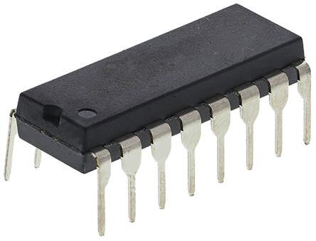
| 描述 | IC COMPLEMENT PWR DRIVER 16-DIP门驱动器 Comp High Speed Power Driver |
| 产品分类 | PMIC - MOSFET,电桥驱动器 - 外部开关集成电路 - IC |
| 品牌 | Texas Instruments |
| 产品手册 | |
| 产品图片 |
|
| rohs | 符合RoHS无铅 / 符合限制有害物质指令(RoHS)规范要求 |
| 产品系列 | 电源管理 IC,门驱动器,Texas Instruments UC3707N- |
| 数据手册 | |
| 产品型号 | UC3707N |
| 上升时间 | 60 ns |
| 下降时间 | 65 ns |
| 产品目录页面 | |
| 产品种类 | 门驱动器 |
| 供应商器件封装 | 16-PDIP |
| 其它名称 | 296-11243-5 |
| 包装 | 管件 |
| 单位重量 | 1.054 g |
| 商标 | Texas Instruments |
| 安装类型 | 通孔 |
| 安装风格 | Through Hole |
| 封装 | Tube |
| 封装/外壳 | 16-DIP(0.300",7.62mm) |
| 封装/箱体 | PDIP-16 |
| 工作温度 | 0°C ~ 70°C |
| 工厂包装数量 | 25 |
| 延迟时间 | 100ns |
| 最大功率耗散 | 2000 mW |
| 最大工作温度 | + 70 C |
| 最小工作温度 | 0 C |
| 标准包装 | 25 |
| 激励器数量 | 2 Driver |
| 电压-电源 | 5 V ~ 40 V |
| 电流-峰值 | 1.5A |
| 电源电压-最小 | 5 V |
| 电源电流 | 15 mA |
| 类型 | High Speed |
| 系列 | UC3707 |
| 输入类型 | 反相和非反相 |
| 输出数 | 2 |
| 输出端数量 | 2 |
| 配置 | 低端 |
| 配置数 | 2 |
| 高压侧电压-最大值(自举) | - |


- 商务部:美国ITC正式对集成电路等产品启动337调查
- 曝三星4nm工艺存在良率问题 高通将骁龙8 Gen1或转产台积电
- 太阳诱电将投资9.5亿元在常州建新厂生产MLCC 预计2023年完工
- 英特尔发布欧洲新工厂建设计划 深化IDM 2.0 战略
- 台积电先进制程称霸业界 有大客户加持明年业绩稳了
- 达到5530亿美元!SIA预计今年全球半导体销售额将创下新高
- 英特尔拟将自动驾驶子公司Mobileye上市 估值或超500亿美元
- 三星加码芯片和SET,合并消费电子和移动部门,撤换高东真等 CEO
- 三星电子宣布重大人事变动 还合并消费电子和移动部门
- 海关总署:前11个月进口集成电路产品价值2.52万亿元 增长14.8%


PDF Datasheet 数据手册内容提取
UC1707, UC2707, UC3707 www.ti.com............................................................................................................................................. SLUS177B–MARCH1999–REVISEDSEPTEMBER2008 DUAL CHANNEL POWER DRIVER FEATURES • AnalogShutdownWithOptionalLatch 1 • TwoIndependentDrivers • LowQuiescentCurrent • 1.5ATotemPoleOutputs • 5Vto40VOperation • InvertingandNon-InvertingInputs • ThermalShutdownProtection • 40nsRiseandFallInto1000pF • 16-PinDual-In-LinePackage • High-Speed,PowerMOSFETCompatible • 20-PinPLCCandCLCCPackage • LowCross-ConductionCurrentSpike DESCRIPTION The UC1707 family of power drivers is made with a high-speed Schottky process to interface between low-level control functions and high-power switching devices–particularly power MOSFETs. These devices contain two independentchannels,eachofwhichcanbeactivatedbyeitherahighorlowinputlogiclevelsignal.Each output cansourceorsinkupto1.5Aaslongaspowerdissipationlimitsarenotexceeded. Althougheachoutputcanbeactivatedindependentlywithitsowninputs, it can be forced low in common through the action either of a digital high signal at the Shutdown terminal or a differential low-level analog signal. The Shutdown command from either source can either be latching or not, depending on the status of the Latch Disablepin. SupplyvoltageforbothV andV canindependentlyrangefrom5Vto40V. IN C These devices are available in two-watt plastic "bat-wing" DIP for operation over a 0°C to 70°C temperature range and, with reduced power, in a hermetically sealed cerdip for –55°C to +125°C operation. Also available in surfacemountDW,Q,Lpackages. TRUTHTABLE (EachChannel)(1) INV. N.I. OUT H H L L H H H L L L L L (1) OUT=INVandN.I. OUT=INVorN.I. 1 Pleasebeawarethatanimportantnoticeconcerningavailability,standardwarranty,anduseincriticalapplicationsofTexas Instrumentssemiconductorproductsanddisclaimerstheretoappearsattheendofthisdatasheet. PRODUCTIONDATAinformationiscurrentasofpublicationdate. Copyright©1999–2008,TexasInstrumentsIncorporated Products conform to specifications per the terms of the Texas Instruments standard warranty. Production processing does not necessarilyincludetestingofallparameters.
UC1707, UC2707, UC3707 SLUS177B–MARCH1999–REVISEDSEPTEMBER2008............................................................................................................................................. www.ti.com BLOCK DIAGRAM CONNECTION DIAGRAMS 2 SubmitDocumentationFeedback Copyright©1999–2008,TexasInstrumentsIncorporated ProductFolderLink(s):UC1707 UC2707 UC3707
UC1707, UC2707, UC3707 www.ti.com............................................................................................................................................. SLUS177B–MARCH1999–REVISEDSEPTEMBER2008 ABSOLUTE MAXIMUM RATINGS overoperatingfree-airtemperaturerange(unlessotherwisenoted) MIN MAX UNIT V Supplyvoltage N/Jpackage 40 V IN V Collectorsupplyvoltage N/Jpackage 40 V C Outputcurrent(eachoutput,sourceorsink)steady-state N/Jpackage ±500 mA Npackage ±1.5 Peaktransient A Jpackage ±1.0 Npackage 20 Capacitivedischargeenergy mJ Jpackage 15 Digitalinputs(1) N/J-package 5.5 V Analogstopinputs N/Jpackage V IN Npackage 2 PowerdissipationatT =25°C W A Jpackage 1 Npackage 5 PowerdissipationatT(leads/case)=25°C(1) W Jpackage 2 Operatingtemperaturerange –55 +125 °C Storagetemperaturerange –65 +150 °C Leadtemperature(soldering,10seconds) 300 °C (1) Allvoltagesarewithrespecttothefourgroundpinswhichmustbeconnectedtogether.Allcurrentsarepositiveinto,negativeoutofthe specifiedterminal.Digitaldrivecanexceed5.5Vifinputcurrentislimitedto10mA.Consultpackagingsectionofdatabookforthermal limitationsandconsiderationsofpackage. ELECTRICAL CHARACTERISTICS Unlessotherwisestated,thesespecificationsapplyforT =–55°Cto+125°CfortheUC1707,–25°Cto+85°Cforthe A UC2707,and0°Cto+70°CfortheUC3707;V =V =20V.T =T. IN C A J PARAMETER TESTCONDITIONS MIN TYP MAX UNIT V Supplycurrent V =40V 12 15 mA IN IN V Supplycurrent V =40V,outputslow 5.2 7.5 mA C C V Leakagecurrent V =0,V -30V,noload 0.05 0.1 mA C IN C Digitalinputlowlevel 0.8 V Digitalinputhighlevel 2.2 V Inputcurrent V =0 –0.06 –1.0 mA I Inputleakage V =5V 0.05 0.1 mA I I =–50mA 2.0 O V –V Outputhighsat. V C O I =–500mA 2.5 O I =–50mA 0.4 O V Outputlowsat. V O I =–500mA 2.5 O Analogthreshold V =0to15V 100 130 160 mV CM Inputbiascurrent V =0 –10 –20 m A CM Thermalshutdown 155 °C Shutdownthreshold Pin7input 0.4 1.0 2.2 V Latchdisablethreshold Pin3input 0.8 1.2 2.2 V Copyright©1999–2008,TexasInstrumentsIncorporated SubmitDocumentationFeedback 3 ProductFolderLink(s):UC1707 UC2707 UC3707
UC1707, UC2707, UC3707 SLUS177B–MARCH1999–REVISEDSEPTEMBER2008............................................................................................................................................. www.ti.com TYPICAL SWITCHING CHARACTERISTICS V =V =20V,T =25°C.Delaysmeasuredto10%outputchange. IN C A PARAMETER TESTCONDITIONS OUTPUTCL= UNIT FromInv.InputtoOutput open 1.0 2.2 nF Risetimedelay 40 50 60 ns 10%to90%rise 25 40 50 ns Falltimedelay 30 40 50 ns 90%to10%fall 25 40 50 ns FromN.I.InputtoOutput Risetimedelay 30 40 50 ns 10%to90%rise 25 40 50 ns Falltimedelay 45 55 65 ns 90%to10%fall 25 40 50 ns V cross-conductioncurrentspikeduration Outputrise 25 ns C Outputfall 0 ns Analogshutdowndelay Stopnon-Inv.=0V 180 ns StopInv.=0to0.5V 180 ns Digitalshutdowndelay 2VinputonPin7 50 ns 4 SubmitDocumentationFeedback Copyright©1999–2008,TexasInstrumentsIncorporated ProductFolderLink(s):UC1707 UC2707 UC3707
UC1707, UC2707, UC3707 www.ti.com............................................................................................................................................. SLUS177B–MARCH1999–REVISEDSEPTEMBER2008 SIMPLIFIED INTERNAL CIRCUITRY Figure1.TypicalDigitalInputGate Figure2.TypicalDigitalInputGate Figure3.LatchDisable Copyright©1999–2008,TexasInstrumentsIncorporated SubmitDocumentationFeedback 5 ProductFolderLink(s):UC1707 UC2707 UC3707
UC1707, UC2707, UC3707 SLUS177B–MARCH1999–REVISEDSEPTEMBER2008............................................................................................................................................. www.ti.com SIMPLIFIED INTERNAL CIRCUITRY (continued) Figure4.UseoftheShutdownPin SHUTDOWNCIRCUITDESCRIPTION The function of the circuitry is to be able to provide a shutdown of the device. This is defined as functionality that willdrivebothoutputstothelowstate.Therearethreedifferentinputsthatgovernthisshutdowncapability. • AnalogStopPins—Thedifferentialinputstothiscomparatorprovideawaytoexecuteashutdown. • Latch Disable Pin — Assuming that the Shutdown pin is left open, a high on this pin disables the latching functionality of the Analog Stop shutdown. A low on this pin enables the latching functionality of the Analog Stop shutdown. If a shutdown occurs through the Analog Stop circuit while Latch Disable is high, then the outputs will go low, but will return to normal operation as soon as the Analog Stop circuit allows it. If a shutdown occurs through the Analog Stop circuit while Latch Disable is low, then the outputs will go low and remain low even if the Analog Stop circuit no longer drives the shutdown. The outputs will remain "latched" low (in shutdown) until the Latch Disable goes high and the Analog Stop circuit allows it to return from shutdownortheVINvoltageiscycledto0Vandthenreturnedabove5V. • ShutdownPin—Thispinservestwopurposes. 1. ItcanbeusedasanoutputoftheAnalogStopcircuit. 2. It can be used as an input to force a shutdown or to force the device out of shutdown. This pin can override both the Analog Stop circuit as well as the Latch Disable Pin. When driving hard logic levels into theShutdownpin,theLatchDisablefunctionalitywillbeoverriddenandthe Latch Disable will not function as it does when used in conjunction with the Analog Stop circuit. When the Shutdown pin is high, the outputs will be in the low state (shutdown). When the Shutdown pin is low (hard logic low) the outputs will operatenormally,regardlessofthestateoftheLatchDisablepinortheAnalogStoppins. In order to use the Shutdown Pin with the Latch Disable functional it is necessary to use either a diode in series with the Shutdown signal or to use an open collector pull-up so that the Shutdown pin is not pulled low. This configurationwillallowtheLatchDisablefunctiontoworkwiththeShutdownpin. 6 SubmitDocumentationFeedback Copyright©1999–2008,TexasInstrumentsIncorporated ProductFolderLink(s):UC1707 UC2707 UC3707
UC1707, UC2707, UC3707 www.ti.com............................................................................................................................................. SLUS177B–MARCH1999–REVISEDSEPTEMBER2008 SIMPLIFIED INTERNAL CIRCUITRY (continued) UG1707SHUTDOWNTRUTHTABLE ANALOGSTOP PREVIOUSSTATEOF SHUTDOWN LATCHDISABLE OUTPUT LOGIC OUTPUT X 0 X X FollowsInputLogic X 1 X X Low(Shutdown) 1 Open X X Low(Shutdown) 0 Open 0 Shutdown (1)LatchedShutdown 0 Open 0 Normal FollowsInputLogic 0 Open 1 X FollowsInputLogic (1) IftheoutputwaspreviouslyinShutdownandLatchDisablewaslowandstayslow,theneveniftheAnalogStopLogicischangedorthe Shutdownpinisopen,theoutputswillremaininShutdown. Figure5.TransformerCoupledPush-PullMOSFETDriveCircuit Figure6.CurrentLimiting Copyright©1999–2008,TexasInstrumentsIncorporated SubmitDocumentationFeedback 7 ProductFolderLink(s):UC1707 UC2707 UC3707
UC1707, UC2707, UC3707 SLUS177B–MARCH1999–REVISEDSEPTEMBER2008............................................................................................................................................. www.ti.com Figure7.Over-VoltageProtection Figure8.PowerMOSFETDriveCircuit Figure9.ChargePumpCircuits 8 SubmitDocumentationFeedback Copyright©1999–2008,TexasInstrumentsIncorporated ProductFolderLink(s):UC1707 UC2707 UC3707
UC1707, UC2707, UC3707 www.ti.com............................................................................................................................................. SLUS177B–MARCH1999–REVISEDSEPTEMBER2008 Figure10.PowerBipolarDriveCircuit Figure11.TransformerCoupledMOSFETDriveCircuit Copyright©1999–2008,TexasInstrumentsIncorporated SubmitDocumentationFeedback 9 ProductFolderLink(s):UC1707 UC2707 UC3707
UC1707, UC2707, UC3707 SLUS177B–MARCH1999–REVISEDSEPTEMBER2008............................................................................................................................................. www.ti.com Figure12.PowerMOSFETDriveCircuitUsingNegativeBiasVoltage andLevelShiftingtoGroundReferencePWM 10 SubmitDocumentationFeedback Copyright©1999–2008,TexasInstrumentsIncorporated ProductFolderLink(s):UC1707 UC2707 UC3707
PACKAGE OPTION ADDENDUM www.ti.com 6-Feb-2020 PACKAGING INFORMATION Orderable Device Status Package Type Package Pins Package Eco Plan Lead/Ball Finish MSL Peak Temp Op Temp (°C) Device Marking Samples (1) Drawing Qty (2) (6) (3) (4/5) 5962-87619012A ACTIVE LCCC FK 20 1 TBD POST-PLATE N / A for Pkg Type -55 to 125 5962- 87619012A UC1707L/ 81032 5962-8761901EA ACTIVE CDIP J 16 1 TBD Call TI N / A for Pkg Type -55 to 125 5962-8761901EA UC1707J/80900 5962-8761901V2A ACTIVE LCCC FK 20 1 TBD POST-PLATE N / A for Pkg Type -55 to 125 5962- 8761901V2A UC1707L QMLV 5962-8761901VEA ACTIVE CDIP J 16 1 TBD Call TI N / A for Pkg Type -55 to 125 5962-8761901VE A UC1707JQMLV 5962-8761903V2A ACTIVE LCCC FK 20 1 TBD POST-PLATE N / A for Pkg Type -55 to 125 5962- 8761903V2A UC1707L-SP 5962-8761903VEA ACTIVE CDIP J 16 1 TBD Call TI N / A for Pkg Type -55 to 125 5962-8761903VE A UC1707J-SP 5962-8761903VFA ACTIVE CFP W 16 1 TBD Call TI N / A for Pkg Type -55 to 125 5962-8761903VF A UC1707W-SP UC1707J ACTIVE CDIP J 16 1 TBD Call TI N / A for Pkg Type -55 to 125 UC1707J UC1707J883B ACTIVE CDIP J 16 1 TBD Call TI N / A for Pkg Type -55 to 125 UC1707J/883B UC1707L ACTIVE LCCC FK 20 1 TBD POST-PLATE N / A for Pkg Type -55 to 125 UC1707L UC1707L883B ACTIVE LCCC FK 20 1 TBD POST-PLATE N / A for Pkg Type -55 to 125 UC1707L/ 883B UC2707DW ACTIVE SOIC DW 16 40 Green (RoHS NIPDAU Level-2-260C-1 YEAR -40 to 85 UC2707DW & no Sb/Br) UC2707DWTR ACTIVE SOIC DW 16 2000 Green (RoHS NIPDAU Level-2-260C-1 YEAR -40 to 85 UC2707DW & no Sb/Br) UC2707N ACTIVE PDIP N 16 25 Green (RoHS NIPDAU N / A for Pkg Type -40 to 85 UC2707N & no Sb/Br) Addendum-Page 1
PACKAGE OPTION ADDENDUM www.ti.com 6-Feb-2020 Orderable Device Status Package Type Package Pins Package Eco Plan Lead/Ball Finish MSL Peak Temp Op Temp (°C) Device Marking Samples (1) Drawing Qty (2) (6) (3) (4/5) UC2707NG4 ACTIVE PDIP N 16 25 Green (RoHS NIPDAU N / A for Pkg Type -40 to 85 UC2707N & no Sb/Br) UC3707DW ACTIVE SOIC DW 16 40 Green (RoHS NIPDAU Level-2-260C-1 YEAR 0 to 70 UC3707DW & no Sb/Br) UC3707DWTR ACTIVE SOIC DW 16 2000 Green (RoHS NIPDAU Level-2-260C-1 YEAR 0 to 70 UC3707DW & no Sb/Br) UC3707J ACTIVE CDIP J 16 1 TBD Call TI N / A for Pkg Type 0 to 70 UC3707J UC3707N ACTIVE PDIP N 16 25 Green (RoHS NIPDAU N / A for Pkg Type 0 to 70 UC3707N & no Sb/Br) UC3707NG4 ACTIVE PDIP N 16 25 Green (RoHS NIPDAU N / A for Pkg Type 0 to 70 UC3707N & no Sb/Br) (1) The marketing status values are defined as follows: ACTIVE: Product device recommended for new designs. LIFEBUY: TI has announced that the device will be discontinued, and a lifetime-buy period is in effect. NRND: Not recommended for new designs. Device is in production to support existing customers, but TI does not recommend using this part in a new design. PREVIEW: Device has been announced but is not in production. Samples may or may not be available. OBSOLETE: TI has discontinued the production of the device. (2) RoHS: TI defines "RoHS" to mean semiconductor products that are compliant with the current EU RoHS requirements for all 10 RoHS substances, including the requirement that RoHS substance do not exceed 0.1% by weight in homogeneous materials. Where designed to be soldered at high temperatures, "RoHS" products are suitable for use in specified lead-free processes. TI may reference these types of products as "Pb-Free". RoHS Exempt: TI defines "RoHS Exempt" to mean products that contain lead but are compliant with EU RoHS pursuant to a specific EU RoHS exemption. Green: TI defines "Green" to mean the content of Chlorine (Cl) and Bromine (Br) based flame retardants meet JS709B low halogen requirements of <=1000ppm threshold. Antimony trioxide based flame retardants must also meet the <=1000ppm threshold requirement. (3) MSL, Peak Temp. - The Moisture Sensitivity Level rating according to the JEDEC industry standard classifications, and peak solder temperature. (4) There may be additional marking, which relates to the logo, the lot trace code information, or the environmental category on the device. (5) Multiple Device Markings will be inside parentheses. Only one Device Marking contained in parentheses and separated by a "~" will appear on a device. If a line is indented then it is a continuation of the previous line and the two combined represent the entire Device Marking for that device. (6) Lead/Ball Finish - Orderable Devices may have multiple material finish options. Finish options are separated by a vertical ruled line. Lead/Ball Finish values may wrap to two lines if the finish value exceeds the maximum column width. Addendum-Page 2
PACKAGE OPTION ADDENDUM www.ti.com 6-Feb-2020 Important Information and Disclaimer:The information provided on this page represents TI's knowledge and belief as of the date that it is provided. TI bases its knowledge and belief on information provided by third parties, and makes no representation or warranty as to the accuracy of such information. Efforts are underway to better integrate information from third parties. TI has taken and continues to take reasonable steps to provide representative and accurate information but may not have conducted destructive testing or chemical analysis on incoming materials and chemicals. TI and TI suppliers consider certain information to be proprietary, and thus CAS numbers and other limited information may not be available for release. In no event shall TI's liability arising out of such information exceed the total purchase price of the TI part(s) at issue in this document sold by TI to Customer on an annual basis. OTHER QUALIFIED VERSIONS OF UC1707, UC1707-SP, UC3707, UC3707M : •Catalog: UC3707, UC1707, UC3707M, UC3707 •Military: UC1707, UC1707 •Space: UC1707-SP NOTE: Qualified Version Definitions: •Catalog - TI's standard catalog product •Military - QML certified for Military and Defense Applications •Space - Radiation tolerant, ceramic packaging and qualified for use in Space-based application Addendum-Page 3
PACKAGE MATERIALS INFORMATION www.ti.com 26-Jan-2013 TAPE AND REEL INFORMATION *Alldimensionsarenominal Device Package Package Pins SPQ Reel Reel A0 B0 K0 P1 W Pin1 Type Drawing Diameter Width (mm) (mm) (mm) (mm) (mm) Quadrant (mm) W1(mm) UC2707DWTR SOIC DW 16 2000 330.0 16.4 10.75 10.7 2.7 12.0 16.0 Q1 UC3707DWTR SOIC DW 16 2000 330.0 16.4 10.75 10.7 2.7 12.0 16.0 Q1 PackMaterials-Page1
PACKAGE MATERIALS INFORMATION www.ti.com 26-Jan-2013 *Alldimensionsarenominal Device PackageType PackageDrawing Pins SPQ Length(mm) Width(mm) Height(mm) UC2707DWTR SOIC DW 16 2000 367.0 367.0 38.0 UC3707DWTR SOIC DW 16 2000 367.0 367.0 38.0 PackMaterials-Page2
IMPORTANTNOTICEANDDISCLAIMER TI PROVIDES TECHNICAL AND RELIABILITY DATA (INCLUDING DATASHEETS), DESIGN RESOURCES (INCLUDING REFERENCE DESIGNS), APPLICATION OR OTHER DESIGN ADVICE, WEB TOOLS, SAFETY INFORMATION, AND OTHER RESOURCES “AS IS” AND WITH ALL FAULTS, AND DISCLAIMS ALL WARRANTIES, EXPRESS AND IMPLIED, INCLUDING WITHOUT LIMITATION ANY IMPLIED WARRANTIES OF MERCHANTABILITY, FITNESS FOR A PARTICULAR PURPOSE OR NON-INFRINGEMENT OF THIRD PARTY INTELLECTUAL PROPERTY RIGHTS. These resources are intended for skilled developers designing with TI products. You are solely responsible for (1) selecting the appropriate TI products for your application, (2) designing, validating and testing your application, and (3) ensuring your application meets applicable standards, and any other safety, security, or other requirements. These resources are subject to change without notice. TI grants you permission to use these resources only for development of an application that uses the TI products described in the resource. Other reproduction and display of these resources is prohibited. No license is granted to any other TI intellectual property right or to any third party intellectual property right. TI disclaims responsibility for, and you will fully indemnify TI and its representatives against, any claims, damages, costs, losses, and liabilities arising out of your use of these resources. TI’s products are provided subject to TI’s Terms of Sale (www.ti.com/legal/termsofsale.html) or other applicable terms available either on ti.com or provided in conjunction with such TI products. TI’s provision of these resources does not expand or otherwise alter TI’s applicable warranties or warranty disclaimers for TI products. Mailing Address: Texas Instruments, Post Office Box 655303, Dallas, Texas 75265 Copyright © 2020, Texas Instruments Incorporated