ICGOO在线商城 > 集成电路(IC) > PMIC - 栅极驱动器 > UC3705N
 Datasheet下载
- 型号: UC3705N
- 制造商: Texas Instruments
- 库位|库存: xxxx|xxxx
- 要求:
| 数量阶梯 | 香港交货 | 国内含税 |
| +xxxx | $xxxx | ¥xxxx |
查看当月历史价格
查看今年历史价格
UC3705N产品简介:
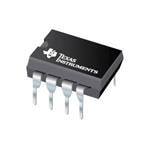
ICGOO电子元器件商城为您提供UC3705N由Texas Instruments设计生产,在icgoo商城现货销售,并且可以通过原厂、代理商等渠道进行代购。 UC3705N价格参考¥35.56-¥66.39。Texas InstrumentsUC3705N封装/规格:PMIC - 栅极驱动器, Low-Side Gate Driver IC Inverting, Non-Inverting 8-PDIP。您可以下载UC3705N参考资料、Datasheet数据手册功能说明书,资料中有UC3705N 详细功能的应用电路图电压和使用方法及教程。
Texas Instruments(德州仪器)的UC3705N是一款PMIC(电源管理集成电路)中的栅极驱动器,主要用于驱动功率MOSFET或IGBT等功率开关器件。其应用场景主要包括以下几个方面:

1. 开关电源(SMPS)设计:
   UC3705N适用于各种开关电源应用,包括AC-DC和DC-DC转换器。它能够高效驱动功率MOSFET或IGBT,从而实现高效的电压转换和稳定的输出。

2. 电机驱动控制:
   在电机驱动系统中,UC3705N可以用于驱动逆变器桥中的功率开关管,支持无刷直流电机(BLDC)、步进电机和其他类型的电机控制。

3. 工业电源和UPS系统:
   该器件适用于工业级电源和不间断电源(UPS)系统,提供高可靠性和高效能的功率开关驱动能力,确保系统的稳定运行。

4. 太阳能逆变器:
   在光伏逆变器中,UC3705N可用于驱动功率开关管,将直流电转换为交流电,满足太阳能发电系统的能量转换需求。

5. 汽车电子:
   虽然UC3705N并非专为汽车设计,但在某些非关键车载应用中,它可以用于驱动功率器件,例如电池管理系统(BMS)中的功率转换部分。

6. 照明系统:
   在LED驱动电源或其他高效照明系统中,UC3705N可作为功率开关驱动器,提高电源效率并降低功耗。

总体而言,UC3705N以其高性能和可靠性,广泛应用于需要高效功率转换和驱动的场景,特别是在需要快速开关和低损耗的场合中表现优异。
| 参数 | 数值 |
| 产品目录 | 集成电路 (IC)半导体 |
| 描述 | IC COMPLEMENT POWER DRIVER 8-DIP门驱动器 Comp Hi-Speed Power Driver |
| 产品分类 | PMIC - MOSFET,电桥驱动器 - 外部开关集成电路 - IC |
| 品牌 | Texas Instruments |
| 产品手册 | |
| 产品图片 |
|
| rohs | 符合RoHS无铅 / 符合限制有害物质指令(RoHS)规范要求 |
| 产品系列 | 电源管理 IC,门驱动器,Texas Instruments UC3705N- |
| 数据手册 | |
| 产品型号 | UC3705N |
| 上升时间 | 40 ns |
| 下降时间 | 40 ns |
| 产品目录页面 | |
| 产品种类 | 门驱动器 |
| 供应商器件封装 | 8-PDIP |
| 其它名称 | 296-11240-5 |
| 包装 | 管件 |
| 单位重量 | 528.600 mg |
| 商标 | Texas Instruments |
| 安装类型 | 通孔 |
| 安装风格 | Through Hole |
| 封装 | Tube |
| 封装/外壳 | 8-DIP(0.300",7.62mm) |
| 封装/箱体 | PDIP-8 |
| 工作温度 | 0°C ~ 70°C |
| 工厂包装数量 | 50 |
| 延迟时间 | 100ns |
| 最大功率耗散 | 1000 mW |
| 最大工作温度 | + 70 C |
| 最小工作温度 | 0 C |
| 标准包装 | 50 |
| 激励器数量 | 1 Driver |
| 电压-电源 | 5 V ~ 40 V |
| 电流-峰值 | 1.5A |
| 电源电压-最大 | 40 V |
| 电源电压-最小 | 5 V |
| 电源电流 | 4 mA |
| 类型 | High Speed |
| 系列 | UC3705 |
| 输入类型 | 反相和非反相 |
| 输出数 | 1 |
| 输出电流 | 1.5 A |
| 输出端数量 | 1 |
| 配置 | 低端 |
| 配置数 | 1 |
| 高压侧电压-最大值(自举) | - |


- 商务部:美国ITC正式对集成电路等产品启动337调查
- 曝三星4nm工艺存在良率问题 高通将骁龙8 Gen1或转产台积电
- 太阳诱电将投资9.5亿元在常州建新厂生产MLCC 预计2023年完工
- 英特尔发布欧洲新工厂建设计划 深化IDM 2.0 战略
- 台积电先进制程称霸业界 有大客户加持明年业绩稳了
- 达到5530亿美元!SIA预计今年全球半导体销售额将创下新高
- 英特尔拟将自动驾驶子公司Mobileye上市 估值或超500亿美元
- 三星加码芯片和SET,合并消费电子和移动部门,撤换高东真等 CEO
- 三星电子宣布重大人事变动 还合并消费电子和移动部门
- 海关总署:前11个月进口集成电路产品价值2.52万亿元 增长14.8%


PDF Datasheet 数据手册内容提取
UC1705 UC2705, UC3705 www.ti.com SLUS370D–JULY1995–REVISEDMARCH2012 HIGH SPEED POWER DRIVER CheckforSamples:UC1705,UC2705,UC3705 FEATURES 1 • 1.5ASource/SinkDrive • LowQuiescentCurrent • 100nsecDelay • 5Vto40VOperation • 40nsecRiseFallinto1000pF • ThermalShutdownProtection • InvertingandNon-InvertingInputs • MinidipandPowerPackages • LowCross-ConductionCurrentSpike DESCRIPTION The UC1705 family of power drivers is made with a high sppeed Schottky process to interface between low-level control functions and high-power switching devices - particularly power MOSFETs. These devices are also an optimum choise for capacitive line drivers where up to 1.5 A may be switched in either direction. With both inverting and non-inverting inputs available, logic signals of either polarity may be accepted, or one input can be usedtogateorstrobetheother. Supply voltages for both V and V can independently range from 5 V to 40 V. For additional application details, S C seetheUC1707/3707datasheet(SLUS177). The UC1705 is packaged in an 8-pin hermetically sealed CERDIP for -55°C to 125°C operation. The UC3705 is specified for a temperature range of 0°C to 70°C and is available in either a plastic minidip or a 5-pin, power TO-220package. TRUTH TABLE(1)(2) INV N.I OUT H H L L H H H L L L L L (1) OUT=INVandN.I. (2) OUT=INVandN.i. BLOCK DIAGRAM 1 Pleasebeawarethatanimportantnoticeconcerningavailability,standardwarranty,anduseincriticalapplicationsof TexasInstrumentssemiconductorproductsanddisclaimerstheretoappearsattheendofthisdatasheet. PRODUCTIONDATAinformationiscurrentasofpublicationdate. Copyright©1995–2012,TexasInstrumentsIncorporated Products conform to specifications per the terms of the Texas Instruments standard warranty. Production processing does not necessarilyincludetestingofallparameters.
UC1705 UC2705, UC3705 SLUS370D–JULY1995–REVISEDMARCH2012 www.ti.com Thesedeviceshavelimitedbuilt-inESDprotection.Theleadsshouldbeshortedtogetherorthedeviceplacedinconductivefoam duringstorageorhandlingtopreventelectrostaticdamagetotheMOSgates. CONNECTION DIAGRAMS DIL-8MINIDIP,SOIC-8 5-PINTO-220 (TOPVIEW) (TOPVIEW) N,JGORDPACKAGE TPACKAGE xxx xxx 5 N.I. IN VS 1 8 N.I. IN 4 INV. IN 3 GND VC 2 7 INV. IN 2 OUT 1 V + V C S LOGIC N/C 3 6 GND OUT 4 5 PWR GND LCCC-20 (TOPVIEW) FKPACKAGE xxx D N G N N C N.I. I INV. I LOGI N/C N/C 3 2 1 20 19 N/C 4 18 N/C N/C 5 17 PWR GND N/C 6 16 OUT N/C 7 15 V C N/C 8 14 N/C 9 10 11 12 13 C S C C C N/ V N/ N/ N/ 2 SubmitDocumentationFeedback Copyright©1995–2012,TexasInstrumentsIncorporated ProductFolderLink(s):UC1705UC2705 UC3705
UC1705 UC2705, UC3705 www.ti.com SLUS370D–JULY1995–REVISEDMARCH2012 ABSOLUTE MAXIMUM RATINGS(1) VALUE UNIT N-Pkg JG-Pkg T-Pkg SupplyVoltage(V ) 40 40 40 V IN CollectorSupplyVoltage,V 40 40 40 C Outputcurrent(sourceorsink) Steady-State ±500 ±500 ±1 A PeakTransient ±1.5 ±1 ±2 A CapacitiveDischargeEnergy 20 15 50 µJ DigitalInputs (2) 5.5 5.5 5.5 V PowerDissipationatT =25°C (1) 1 1 3 W A PowerDissipationatT (Lead/Case)=25°C (1) 3 2 25 W A OperatingTemperatureRange 0to70 –55to125 0to70 °C Storagetemperaturee –65to150 –65to150 –65to150 °C (1) Allcurrentsarepositiveinto,negativeoutofthespecifiedterminal. (2) DigitalDrivecanexceed5.5Viftheinputcurrentislimitedto10mA ELECTRICAL CHARACTERISTICS Unlessotherwisestated,thesespecificationsapplyforT =–55°Cto+125°CfortheUC1705,–25°Cto+85°Cforthe A UC2707,and0°Cto+70°CfortheUC3705;V =V =20V.T =T. IN C A J PARAMETER TESTCONDITIONS MIN TYP MAX UNIT V =40V,outputshigh,Tpackage 6 8 mA S V Supplycurrent S V =40V,outputslow,Tpackage 6 12 mA C V Supplycurrent(N,JGOnly) V =40V,outputslow 2 4 mA C C V Leakagecurrent(N,JGOnly) V =0,V =30V 0.05 0.1 mA C S C Digitalinputlowlevel 0.8 V Digitalinputhighlevel 2.2 V Inputcurrent V =0 –0.6 –1 mA I Inputleakage V =5V 0.05 0.1 mA I I =–50mA 2 O V –V Outputhighsaturation V C O I =–500mA 2.5 O I =–50mA 0.4 O V Outputlowsaturation V O I =–500mA 2.5 O Thermalshutdown 155 °C Copyright©1995–2012,TexasInstrumentsIncorporated SubmitDocumentationFeedback 3 ProductFolderLink(s):UC1705UC2705 UC3705
UC1705 UC2705, UC3705 SLUS370D–JULY1995–REVISEDMARCH2012 www.ti.com TYPICAL SWITCHING CHARACTERISTICS V =V =20V,T =25°C.Delaysmeasuredto10%outputchange. IN C A PARAMETER TESTCONDITIONS OUTPUTCL= UNIT FromInv.InputtoOutput open 1 2.2 nF Risetimedelay 60 60 60 ns 10%to90%rise 20 40 60 ns Falltimedelay 60 60 60 ns 90%to10%fall 25 40 50 ns FromN.I.InputtoOutput Risetimedelay 90 90 90 ns 10%to90%rise 20 40 60 ns Falltimedelay 60 60 60 ns 90%to10%fall 25 40 50 ns V cross-conductioncurrentspikeduration Outputrise 25 ns C Outputfall 0 ns 4 SubmitDocumentationFeedback Copyright©1995–2012,TexasInstrumentsIncorporated ProductFolderLink(s):UC1705UC2705 UC3705
UC1705 UC2705, UC3705 www.ti.com SLUS370D–JULY1995–REVISEDMARCH2012 APPLICATION INFORMATION D1,D2:UC3611SchottkyDiodes Figure1. PowerMOSFETDriveCircuit D1,D2:UC3611SchottkyDiodes Figure3. TransformerCoupledMOSFETDRIVE Circuit D1 D2 D1,D2:UC3611SchottkyDiodes Figure2. PowerMOSFETDriveCircuitUsing NegativeBiasVoltageandLevelShiftingto D1 GroundReferencedPWMs D2 Figure4. ChargePumpCircuit Copyright©1995–2012,TexasInstrumentsIncorporated SubmitDocumentationFeedback 5 ProductFolderLink(s):UC1705UC2705 UC3705
UC1705 UC2705, UC3705 SLUS370D–JULY1995–REVISEDMARCH2012 www.ti.com REVISION HISTORY ChangesfromRevisionC(December,2011)toRevisionD Page • DeletedSN54BCT373fromtitleforFKpackageimage ....................................................................................................... 2 6 SubmitDocumentationFeedback Copyright©1995–2012,TexasInstrumentsIncorporated ProductFolderLink(s):UC1705UC2705 UC3705
PACKAGE OPTION ADDENDUM www.ti.com 28-Jul-2020 PACKAGING INFORMATION Orderable Device Status Package Type Package Pins Package Eco Plan Lead finish/ MSL Peak Temp Op Temp (°C) Device Marking Samples (1) Drawing Qty (2) Ball material (3) (4/5) (6) 5962-9579801M2A ACTIVE LCCC FK 20 1 TBD POST-PLATE N / A for Pkg Type -55 to 125 5962- 9579801M2A UC1705L/ 883B 5962-9579801MPA ACTIVE CDIP JG 8 1 TBD SNPB N / A for Pkg Type -55 to 125 9579801MPA UC1705 5962-9579801VPA ACTIVE CDIP JG 8 1 TBD SNPB N / A for Pkg Type -55 to 125 9579801VPA UC1705 UC1705J ACTIVE CDIP JG 8 1 TBD SNPB N / A for Pkg Type -55 to 125 UC1705J UC1705J883B ACTIVE CDIP JG 8 1 TBD SNPB N / A for Pkg Type -55 to 125 9579801MPA UC1705 UC1705L883B ACTIVE LCCC FK 20 1 TBD POST-PLATE N / A for Pkg Type -55 to 125 5962- 9579801M2A UC1705L/ 883B UC2705D ACTIVE SOIC D 8 75 Green (RoHS NIPDAU Level-2-260C-1 YEAR -40 to 85 UC2705D & no Sb/Br) UC2705DG4 ACTIVE SOIC D 8 75 Green (RoHS NIPDAU Level-2-260C-1 YEAR -40 to 85 UC2705D & no Sb/Br) UC2705N ACTIVE PDIP P 8 50 Green (RoHS NIPDAU N / A for Pkg Type -40 to 85 UC2705N & no Sb/Br) UC3705D ACTIVE SOIC D 8 75 Green (RoHS NIPDAU Level-2-260C-1 YEAR 0 to 70 UC3705D & no Sb/Br) UC3705DTR ACTIVE SOIC D 8 2500 Green (RoHS NIPDAU Level-2-260C-1 YEAR 0 to 70 UC3705D & no Sb/Br) UC3705J ACTIVE CDIP JG 8 1 TBD SNPB N / A for Pkg Type 0 to 70 UC3705J UC3705N ACTIVE PDIP P 8 50 Green (RoHS NIPDAU N / A for Pkg Type 0 to 70 UC3705N & no Sb/Br) (1) The marketing status values are defined as follows: ACTIVE: Product device recommended for new designs. LIFEBUY: TI has announced that the device will be discontinued, and a lifetime-buy period is in effect. NRND: Not recommended for new designs. Device is in production to support existing customers, but TI does not recommend using this part in a new design. PREVIEW: Device has been announced but is not in production. Samples may or may not be available. Addendum-Page 1
PACKAGE OPTION ADDENDUM www.ti.com 28-Jul-2020 OBSOLETE: TI has discontinued the production of the device. (2) RoHS: TI defines "RoHS" to mean semiconductor products that are compliant with the current EU RoHS requirements for all 10 RoHS substances, including the requirement that RoHS substance do not exceed 0.1% by weight in homogeneous materials. Where designed to be soldered at high temperatures, "RoHS" products are suitable for use in specified lead-free processes. TI may reference these types of products as "Pb-Free". RoHS Exempt: TI defines "RoHS Exempt" to mean products that contain lead but are compliant with EU RoHS pursuant to a specific EU RoHS exemption. Green: TI defines "Green" to mean the content of Chlorine (Cl) and Bromine (Br) based flame retardants meet JS709B low halogen requirements of <=1000ppm threshold. Antimony trioxide based flame retardants must also meet the <=1000ppm threshold requirement. (3) MSL, Peak Temp. - The Moisture Sensitivity Level rating according to the JEDEC industry standard classifications, and peak solder temperature. (4) There may be additional marking, which relates to the logo, the lot trace code information, or the environmental category on the device. (5) Multiple Device Markings will be inside parentheses. Only one Device Marking contained in parentheses and separated by a "~" will appear on a device. If a line is indented then it is a continuation of the previous line and the two combined represent the entire Device Marking for that device. (6) Lead finish/Ball material - Orderable Devices may have multiple material finish options. Finish options are separated by a vertical ruled line. Lead finish/Ball material values may wrap to two lines if the finish value exceeds the maximum column width. Important Information and Disclaimer:The information provided on this page represents TI's knowledge and belief as of the date that it is provided. TI bases its knowledge and belief on information provided by third parties, and makes no representation or warranty as to the accuracy of such information. Efforts are underway to better integrate information from third parties. TI has taken and continues to take reasonable steps to provide representative and accurate information but may not have conducted destructive testing or chemical analysis on incoming materials and chemicals. TI and TI suppliers consider certain information to be proprietary, and thus CAS numbers and other limited information may not be available for release. In no event shall TI's liability arising out of such information exceed the total purchase price of the TI part(s) at issue in this document sold by TI to Customer on an annual basis. OTHER QUALIFIED VERSIONS OF UC1705, UC1705-SP, UC3705, UC3705M : •Catalog: UC3705, UC1705, UC3705M, UC3705 •Military: UC1705, UC1705 •Space: UC1705-SP NOTE: Qualified Version Definitions: •Catalog - TI's standard catalog product Addendum-Page 2
PACKAGE OPTION ADDENDUM www.ti.com 28-Jul-2020 •Military - QML certified for Military and Defense Applications •Space - Radiation tolerant, ceramic packaging and qualified for use in Space-based application Addendum-Page 3
PACKAGE MATERIALS INFORMATION www.ti.com 14-Jul-2012 TAPE AND REEL INFORMATION *Alldimensionsarenominal Device Package Package Pins SPQ Reel Reel A0 B0 K0 P1 W Pin1 Type Drawing Diameter Width (mm) (mm) (mm) (mm) (mm) Quadrant (mm) W1(mm) UC3705DTR SOIC D 8 2500 330.0 12.4 6.4 5.2 2.1 8.0 12.0 Q1 PackMaterials-Page1
PACKAGE MATERIALS INFORMATION www.ti.com 14-Jul-2012 *Alldimensionsarenominal Device PackageType PackageDrawing Pins SPQ Length(mm) Width(mm) Height(mm) UC3705DTR SOIC D 8 2500 367.0 367.0 35.0 PackMaterials-Page2
None
PACKAGE OUTLINE D0008A SOIC - 1.75 mm max height SCALE 2.800 SMALL OUTLINE INTEGRATED CIRCUIT C SEATING PLANE .228-.244 TYP [5.80-6.19] .004 [0.1] C A PIN 1 ID AREA 6X .050 [1.27] 8 1 2X .189-.197 [4.81-5.00] .150 NOTE 3 [3.81] 4X (0 -15 ) 4 5 8X .012-.020 B .150-.157 [0.31-0.51] .069 MAX [3.81-3.98] .010 [0.25] C A B [1.75] NOTE 4 .005-.010 TYP [0.13-0.25] 4X (0 -15 ) SEE DETAIL A .010 [0.25] .004-.010 0 - 8 [0.11-0.25] .016-.050 [0.41-1.27] DETAIL A (.041) TYPICAL [1.04] 4214825/C 02/2019 NOTES: 1. Linear dimensions are in inches [millimeters]. Dimensions in parenthesis are for reference only. Controlling dimensions are in inches. Dimensioning and tolerancing per ASME Y14.5M. 2. This drawing is subject to change without notice. 3. This dimension does not include mold flash, protrusions, or gate burrs. Mold flash, protrusions, or gate burrs shall not exceed .006 [0.15] per side. 4. This dimension does not include interlead flash. 5. Reference JEDEC registration MS-012, variation AA. www.ti.com
EXAMPLE BOARD LAYOUT D0008A SOIC - 1.75 mm max height SMALL OUTLINE INTEGRATED CIRCUIT 8X (.061 ) [1.55] SYMM SEE DETAILS 1 8 8X (.024) [0.6] SYMM (R.002 ) TYP [0.05] 5 4 6X (.050 ) [1.27] (.213) [5.4] LAND PATTERN EXAMPLE EXPOSED METAL SHOWN SCALE:8X SOLDER MASK SOLDER MASK METAL OPENING OPENING METAL UNDER SOLDER MASK EXPOSED METAL EXPOSED METAL .0028 MAX .0028 MIN [0.07] [0.07] ALL AROUND ALL AROUND NON SOLDER MASK SOLDER MASK DEFINED DEFINED SOLDER MASK DETAILS 4214825/C 02/2019 NOTES: (continued) 6. Publication IPC-7351 may have alternate designs. 7. Solder mask tolerances between and around signal pads can vary based on board fabrication site. www.ti.com
EXAMPLE STENCIL DESIGN D0008A SOIC - 1.75 mm max height SMALL OUTLINE INTEGRATED CIRCUIT 8X (.061 ) [1.55] SYMM 1 8 8X (.024) [0.6] SYMM (R.002 ) TYP [0.05] 5 4 6X (.050 ) [1.27] (.213) [5.4] SOLDER PASTE EXAMPLE BASED ON .005 INCH [0.125 MM] THICK STENCIL SCALE:8X 4214825/C 02/2019 NOTES: (continued) 8. Laser cutting apertures with trapezoidal walls and rounded corners may offer better paste release. IPC-7525 may have alternate design recommendations. 9. Board assembly site may have different recommendations for stencil design. www.ti.com
MECHANICAL DATA MCER001A – JANUARY 1995 – REVISED JANUARY 1997 JG (R-GDIP-T8) CERAMIC DUAL-IN-LINE 0.400 (10,16) 0.355 (9,00) 8 5 0.280 (7,11) 0.245 (6,22) 1 4 0.065 (1,65) 0.045 (1,14) 0.063 (1,60) 0.020 (0,51) MIN 0.310 (7,87) 0.015 (0,38) 0.290 (7,37) 0.200 (5,08) MAX Seating Plane 0.130 (3,30) MIN 0.023 (0,58) 0°–15° 0.015 (0,38) 0.100 (2,54) 0.014 (0,36) 0.008 (0,20) 4040107/C 08/96 NOTES: A. All linear dimensions are in inches (millimeters). B. This drawing is subject to change without notice. C. This package can be hermetically sealed with a ceramic lid using glass frit. D. Index point is provided on cap for terminal identification. E. Falls within MIL STD 1835 GDIP1-T8 • POST OFFICE BOX 655303 DALLAS, TEXAS 75265
None
IMPORTANTNOTICEANDDISCLAIMER TI PROVIDES TECHNICAL AND RELIABILITY DATA (INCLUDING DATASHEETS), DESIGN RESOURCES (INCLUDING REFERENCE DESIGNS), APPLICATION OR OTHER DESIGN ADVICE, WEB TOOLS, SAFETY INFORMATION, AND OTHER RESOURCES “AS IS” AND WITH ALL FAULTS, AND DISCLAIMS ALL WARRANTIES, EXPRESS AND IMPLIED, INCLUDING WITHOUT LIMITATION ANY IMPLIED WARRANTIES OF MERCHANTABILITY, FITNESS FOR A PARTICULAR PURPOSE OR NON-INFRINGEMENT OF THIRD PARTY INTELLECTUAL PROPERTY RIGHTS. These resources are intended for skilled developers designing with TI products. You are solely responsible for (1) selecting the appropriate TI products for your application, (2) designing, validating and testing your application, and (3) ensuring your application meets applicable standards, and any other safety, security, or other requirements. These resources are subject to change without notice. TI grants you permission to use these resources only for development of an application that uses the TI products described in the resource. Other reproduction and display of these resources is prohibited. No license is granted to any other TI intellectual property right or to any third party intellectual property right. TI disclaims responsibility for, and you will fully indemnify TI and its representatives against, any claims, damages, costs, losses, and liabilities arising out of your use of these resources. TI’s products are provided subject to TI’s Terms of Sale (www.ti.com/legal/termsofsale.html) or other applicable terms available either on ti.com or provided in conjunction with such TI products. TI’s provision of these resources does not expand or otherwise alter TI’s applicable warranties or warranty disclaimers for TI products. Mailing Address: Texas Instruments, Post Office Box 655303, Dallas, Texas 75265 Copyright © 2020, Texas Instruments Incorporated