ICGOO在线商城 > 集成电路(IC) > PMIC - PFC(功率因数修正) > UC2854BMDWREP

 Datasheet下载
- 型号: UC2854BMDWREP
- 制造商: Texas Instruments
- 库位|库存: xxxx|xxxx
- 要求:
| 数量阶梯 | 香港交货 | 国内含税 |
| +xxxx | $xxxx | ¥xxxx |
查看当月历史价格
查看今年历史价格
UC2854BMDWREP产品简介:
ICGOO电子元器件商城为您提供UC2854BMDWREP由Texas Instruments设计生产,在icgoo商城现货销售,并且可以通过原厂、代理商等渠道进行代购。 UC2854BMDWREP价格参考¥52.98-¥97.95。Texas InstrumentsUC2854BMDWREP封装/规格:PMIC - PFC(功率因数修正), PFC IC Average Current 80kHz ~ 120kHz 16-SOIC。您可以下载UC2854BMDWREP参考资料、Datasheet数据手册功能说明书,资料中有UC2854BMDWREP 详细功能的应用电路图电压和使用方法及教程。
UC2854BMDWREP 是德州仪器(Texas Instruments)生产的一款用于功率因数校正(PFC)的控制芯片,属于PMIC - PFC(电源管理集成电路 - 功率因数修正)类别。该器件采用8引脚SOIC封装,具备增强型性能和可靠性,符合军用级标准(REP表示抗辐射增强产品),适用于严苛环境下的高可靠性应用。

该芯片主要用于有源功率因数校正电路,常见于连续导通模式(CCM)升压PFC拓扑结构中。其主要功能是通过控制功率开关管,使输入电流跟随输入电压波形,从而提高功率因数、降低谐波失真,满足国际电磁兼容标准(如IEC 61000-3-2)。

典型应用场景包括:工业级开关电源(SMPS)、服务器电源、通信电源、医疗电源设备、航空航天及国防电子系统等对电源效率和稳定性要求较高的领域。由于其具备抗辐射特性,特别适用于空间或高可靠性军工项目中的电源设计。

此外,UC2854BMDWREP 具备过压保护、欠压锁定、软启动等功能,提升了系统安全性与可靠性。其工作温度范围宽,适合在恶劣环境下长期稳定运行,是高性能PFC电源设计中的关键控制元件。
| 参数 | 数值 |
| 产品目录 | 集成电路 (IC) |
| 描述 | IC PFC CTRLR AVERAGE CURR 16SOIC |
| 产品分类 | |
| 品牌 | Texas Instruments |
| 数据手册 | |
| 产品图片 |
|
| 产品型号 | UC2854BMDWREP |
| rohs | 无铅 / 符合限制有害物质指令(RoHS)规范要求 |
| 产品系列 | - |
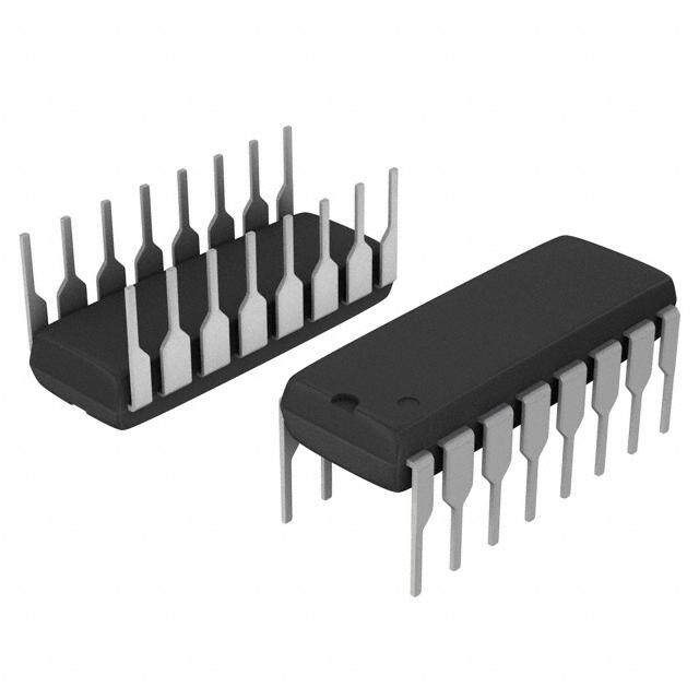
| 供应商器件封装 | 16-SOIC |
| 其它名称 | 296-21935-1 |
| 包装 | 剪切带 (CT) |
| 安装类型 | 表面贴装 |
| 封装/外壳 | 16-SOIC(0.295",7.50mm 宽) |
| 工作温度 | -55°C ~ 125°C |
| 标准包装 | 1 |
| 模式 | 平均电流 |
| 电压-电源 | 10 V ~ 20 V |
| 电流-启动 | 300µA |
| 频率-开关 | 80kHz ~ 120kHz |
.jpg)


- 商务部:美国ITC正式对集成电路等产品启动337调查
- 曝三星4nm工艺存在良率问题 高通将骁龙8 Gen1或转产台积电
- 太阳诱电将投资9.5亿元在常州建新厂生产MLCC 预计2023年完工
- 英特尔发布欧洲新工厂建设计划 深化IDM 2.0 战略
- 台积电先进制程称霸业界 有大客户加持明年业绩稳了
- 达到5530亿美元!SIA预计今年全球半导体销售额将创下新高
- 英特尔拟将自动驾驶子公司Mobileye上市 估值或超500亿美元
- 三星加码芯片和SET,合并消费电子和移动部门,撤换高东真等 CEO
- 三星电子宣布重大人事变动 还合并消费电子和移动部门
- 海关总署:前11个月进口集成电路产品价值2.52万亿元 增长14.8%


PDF Datasheet 数据手册内容提取
Product Sample & Technical Tools & Support & Folder Buy Documents Software Community UC2854B-EP SGLS318A–NOVEMBER2005–REVISEDNOVEMBER2015 UC2854B-EP Advanced High-Power Factor Preregulator 1 Features Comparator • ControlledBaseline • UVLOOptions(16V/10Vor10.5V/10V) 1 – OneAssembly/TestSite,OneFabricationSite • 300-μAStart-UpSupplyCurrent • ExtendedTemperaturePerformanceof−55°Cto 2 Applications 125°C IndustrialLighting • EnhancedDiminishingManufacturingSources (DMS)Support 3 Description • EnhancedProduct-ChangeNotification The UC2854B products are pin compatible enhanced • QualificationPedigree versions of the UC2854. Like the UC2854, these (1) ComponentqualificationinaccordancewithJEDECand products provide all of the functions necessary for industrystandardstoensurereliableoperationoveran active power factor corrected preregulators. The extendedtemperaturerange.Thisincludes,butisnotlimited controller achieves near unity power factor by to,HighlyAcceleratedStressTest(HAST)orbiased85/85, shaping the ac-input line current waveform to temperaturecycle,autoclaveorunbiasedHAST, correspond to the ac-input line voltage. To do this the electromigration,bondintermetalliclife,andmoldcompound life.Suchqualificationtestingshouldnotbeviewedas UC2854B uses average current mode control. justifyinguseofthiscomponentbeyondspecified Average current mode control maintains stable, low performanceandenvironmentallimits. distortion sinusoidal line current without the need for • ControlsBoostPWMtoNear-UnityPowerFactor slope compensation, unlike peak current mode • LimitsLineCurrentDistortionto <3% control. • World-WideOperationWithoutSwitches A 1% 7.5-V reference, fixed frequency oscillator, • AccuratePowerLimiting PWM, voltage amplifier with soft-start, line voltage feedforward (VRMS squarer), input supply voltage • Fixed-FrequencyAverageCurrent-ModeControl clamp, and over current comparator round out the list • HighBandwidth(5MHz),Low-OffsetCurrent offeatures. Amplifier The UC2854B is available in a DW (SOIC-wide) • IntegratedCurrent-andVoltageAmplifierOutput package. Clamps • MultiplierImprovements:Linearity,500mVVAC DeviceInformation(1) Offset(EliminatesExternalResistor),0Vto5V PARTNUMBER PACKAGE BODYSIZE(NOM) MultoutCommon-ModeRange UC2854B-EP SOIC(16) 10.30mm×7.50mm • V GOODComparator REF (1) For all available packages, see the orderable addendum at • FasterandImprovedAccuracyENABLE theendofthedatasheet. BlockDiagram VAO MOUT CAO PKLMT REF 7 5 3 2 9 VCC 7.5 V REF (A) 16 V / 10 V RUN (B) 10.5 V / 10 V ENA 10 IC 7.1 V 2.65 V / 2.15 V POWER 3 V 15 VCC A VSENSE 11 R IAC 6 B R S Q 16 GTDRV 8 X2 C VRMS 14 µA RUN 20 V SS 13 IMOUT ACB OSC 1 GND 4 14 12 ISENSE CT RSET UDG−03110 1 An IMPORTANT NOTICE at the end of this data sheet addresses availability, warranty, changes, use in safety-critical applications, intellectualpropertymattersandotherimportantdisclaimers.PRODUCTIONDATA.
UC2854B-EP SGLS318A–NOVEMBER2005–REVISEDNOVEMBER2015 www.ti.com Table of Contents 1 Features.................................................................. 1 8.3 FeatureDescription.................................................10 2 Applications........................................................... 1 8.4 DeviceFunctionalModes........................................12 3 Description............................................................. 1 9 ApplicationandImplementation........................ 13 4 RevisionHistory..................................................... 2 9.1 ApplicationInformation............................................13 9.2 TypicalApplication .................................................13 5 Description(continued)......................................... 3 10 PowerSupplyRecommendations..................... 29 6 PinConfigurationandFunctions......................... 4 11 Layout................................................................... 29 7 Specifications......................................................... 5 11.1 LayoutGuidelines.................................................29 7.1 AbsoluteMaximumRatings......................................5 11.2 LayoutExample....................................................30 7.2 ESDRatings..............................................................5 12 DeviceandDocumentationSupport................. 31 7.3 RecommendedOperatingConditions.......................5 7.4 ThermalInformation..................................................5 12.1 CommunityResources..........................................31 7.5 ElectricalCharacteristics...........................................6 12.2 Trademarks...........................................................31 7.6 TypicalCharacteristics..............................................8 12.3 ElectrostaticDischargeCaution............................31 12.4 Glossary................................................................31 8 DetailedDescription............................................ 10 13 Mechanical,Packaging,andOrderable 8.1 Overview.................................................................10 Information........................................................... 31 8.2 FunctionalBlockDiagram.......................................10 4 Revision History NOTE:Pagenumbersforpreviousrevisionsmaydifferfrompagenumbersinthecurrentversion. ChangesfromOriginal(November2005)toRevisionA Page • AddedPinFunctionstable,ESDRatingstable,ThermalInformationtable,DetailedDescriptionsection,Application andImplementationsection,PowerSupplyRecommendationssection,Layoutsection,DeviceandDocumentation Supportsection,andMechanical,Packaging,andOrderableInformationsection................................................................ 1 • UpdatedthemaxV turn-onthresholdvoltage.................................................................................................................... 6 CC • Updatedthemaxenablethresholdvoltage............................................................................................................................ 6 2 SubmitDocumentationFeedback Copyright©2005–2015,TexasInstrumentsIncorporated ProductFolderLinks:UC2854B-EP
UC2854B-EP www.ti.com SGLS318A–NOVEMBER2005–REVISEDNOVEMBER2015 5 Description (continued) The UC2854A/B products improve upon the UC2854 by offering a wide bandwidth, low offset current amplifier, a faster responding and improved accuracy enable comparator, a VREF GOOD comparator, UVLO threshold options (16 V/10 V for offline, 10.5 V/10 V for startup from an auxiliary 12-V regulator), lower startup supply current,andanenhancedmultiply/dividecircuit. New features like the amplifier output clamps, improved amplifier current sinking capability, and low offset VAC pin reduce the external component count while improving performance. Improved common mode input range of the multiplier output/current amplifier input allow the designer greater flexibility in choosing a method for current sensing.Unlikeitspredecessor,RSETcontrolsonlyoscillatorchargingcurrentandhasnoeffectonclampingthe maximum multiplier output current. This current is now clamped to a maximum of 2 × IAC at all times which simplifies the design process and provides foldback power limiting during brownout and extreme low line conditions. Copyright©2005–2015,TexasInstrumentsIncorporated SubmitDocumentationFeedback 3 ProductFolderLinks:UC2854B-EP
UC2854B-EP SGLS318A–NOVEMBER2005–REVISEDNOVEMBER2015 www.ti.com 6 Pin Configuration and Functions DWPackage 16-PinSOIC TopView GND 1 16 GTDRV PKLMT 2 15 VCC CAO 3 14 CT ISENSE 4 13 SS MOUT 5 12 RSET IAC 6 11 VSENSE VAO 7 10 ENA VRMS 8 9 VREF PinFunctions PIN I/O DESCRIPTION NAME J/N/DW Q/L OutputofthewidebandwidthcurrentamplifierandoneoftheinputstothePWMduty-cycle CAO 3 4 O comparator.TheoutputsignalgeneratedbythisamplifiercommandsthePWMtoforcethe correctinputcurrent.Theoutputcanswingfrom0.1Vto7.5V. CT 14 18 I CapacitorfromCTtoGNDsetsthePWMoscillatorfrequency Anominalvoltageabove2.65Vonthispinallowsthedevicetobeginoperating.Once ENA 10 13 I operating,thedeviceshutsoffifthispingoesbelow2.15Vnominal. AllbypassandtimingcapacitorsconnectedtoGNDshouldhaveleadsasshortanddirect GND 1 2 — aspossible.AllvoltagesaremeasuredwithrespectGND. OutputofthePWMisa1.5-Apeaktotem-poleMOSFETgatedriveronGTDRV.Thisoutput isinternallyclampedto15VsothatthedevicecanbeoperatedwithVCCashighas35V. GTDRV 16 20 O Useaseriesgateresistorofatleast5Ωtopreventinteractionbetweenthegateimpedance andtheGTDRVoutputdriverthatmightcausetheGTDRVoutputtoovershootexcessively. SomeovershootoftheGTDRVoutputisalwaysexpectedwhendrivingacapacitiveload. Currentinputtothemultiplier,proportionaltotheinstantaneouslinevoltage.Thisinputto theanalogmultiplierisacurrent.Themultiplieristailoredforlowdistortionfromthiscurrent input(IAC)toMOUT,sothisistheonlymultiplierinputthatshouldbeusedforsensing IAC 6 8 I instantaneouslinevoltage.Thenominalvoltageonacis6V,soinadditiontoaresistorfrom IACtorectified60Hz,connectaresistorfromIACtoVREF.IftheresistortoVREFisone- fourthofthevalueoftheresistortotherectifier,thenthe6-Voffsetiscancelled,andtheline currenthasminimalcross-overdistortion. Switchcurrentsensinginput.Thisistheinvertinginputtothecurrentamplifier.Thisinput andthenon-invertinginputMOUTremainfunctionaldowntoandbelowGND.Careshould ISENSE 4 5 I betakentoavoidtakingtheseinputsbelow−0.5V,becausetheyareprotectedwithdiodes toGND. Multiplieroutputandcurrentsenseplus.Theoutputoftheanalogmultiplierandthenon- invertinginputofthecurrentamplifierareconnectedtogetheratMOUT.Thecautionsabout MOUT 5 7 I/O takingISENSEbelow−0.5ValsoapplytoMOUT.Asthemultiplieroutputisacurrent,this isahigh-impedanceinputsimilartoISENSE,sothecurrentamplifiercanbeconfiguredasa differentialamplifiertorejectGNDnoise. Peaklimit.ThethresholdforPKLMTis0V.Connectthisinputtothenegativevoltageonthe PKLMT 2 3 I currentsenseresistor.UsearesistortoREFtooffsetthenegativecurrentsensesignalup toGND. Oscillatorchargingcurrentandmultiplierlimitset.AresistorfromRSETtogroundprograms RSET 12 15 I oscillatorchargingcurrent.Multiplieroutputcurrentdoesnotexceed3.75Vdividedbythe resistorfromRSETtoground. Soft-start.SSremainsatGNDaslongasthedeviceisdisabledorVCCistoolow.SSpulls uptoover8Vbyaninternal14-mAcurrentsourcewhenbothVCCbecomesvalidandthe deviceisenabled.SSactsasthereferenceinputtothevoltageamplifierifSSisbelow SS 13 17 I VREF.WithalargecapacitorfromSStoGND,thereferencetothevoltageregulating amplifierrisesslowly,andincreasethePWMdutycycleslowly.Intheeventofadisable commandorasupplydropout,SSwillquicklydischargetogroundanddisablethePWM. VAO 7 9 I Voltageamplifierinput 4 SubmitDocumentationFeedback Copyright©2005–2015,TexasInstrumentsIncorporated ProductFolderLinks:UC2854B-EP
UC2854B-EP www.ti.com SGLS318A–NOVEMBER2005–REVISEDNOVEMBER2015 PinFunctions(continued) PIN I/O DESCRIPTION NAME J/N/DW Q/L VCC 15 19 I Positivesupplyrail Usedtosetthepeaklimitpointandasaninternalreferenceforvariousdevicefunctions. VREF 9 12 O Thisvoltagemustbepresentforthedevicetooperate. Oneoftheinputsintothemultiplier.ThispinprovidestheinputRMSvoltagetothemultiplier VRMS 8 10 I circuitry. Thispinprovidesthefeedbackfromtheoutput.Thisinputgoesintothevoltageerror VSENSE 11 14 I amplifierandtheoutputoftheerroramplifierisanotheroftheinputsintothemultiplier circuit. 7 Specifications 7.1 Absolute Maximum Ratings overoperatingfree-airtemperaturerange(unlessotherwisenoted)(1) MIN MAX UNIT V Supplyvoltage 22 V CC VSENSE,VRMS,ISENSEMOUT 11 V Inputvoltage PKLMT 5 V I GTDRVcurrent,continuous 0.5 A GTDRV I GTDRVcurrent,50%dutycycle 1.5 A GTDRV Inputcurrent RSET,IAC,PKLMT,ENA 10 mA T Junctiontemperature −55 150 °C J T Leadtemperature,1.6mm(1/16inch)fromcasefor10seconds 300 °C sol T Storagetemperature −65 150 °C stg (1) StressesbeyondthoselistedunderAbsoluteMaximumRatingsmaycausepermanentdamagetothedevice.Thesearestressratings only,whichdonotimplyfunctionaloperationofthedeviceattheseoranyotherconditionsbeyondthoseindicatedunderRecommended OperatingConditions.Exposuretoabsolute-maximum-ratedconditionsforextendedperiodsmayaffectdevicereliability. 7.2 ESD Ratings VALUE UNIT V Electrostaticdischarge Human-bodymodel(HBM),perANSI/ESDA/JEDECJS-001(1) ±2000 V (ESD) (1) JEDECdocumentJEP155statesthat500-VHBMallowssafemanufacturingwithastandardESDcontrolprocess. 7.3 Recommended Operating Conditions overoperatingfree-airtemperaturerange(unlessotherwisenoted) MIN MAX UNIT V Supplyvoltage 10 20 V CC T Operatingjunctiontemperature −55 125 °C J 7.4 Thermal Information UC2854B-EP DW(SOIC) THERMALMETRIC(1) UNIT 16PINS HIGH LOW R Junction-to-ambientthermalresistance (2) 36.9 38.4 °C/W θJA R Junction-to-casethermalresistance 73.1 111.6 °C/W θJC (1) Formoreinformationabouttraditionalandnewthermalmetrics,seetheSemiconductorandICPackageThermalMetricsapplication report,SPRA953. (2) R valuesarebasedonzeroairflow. θJA Copyright©2005–2015,TexasInstrumentsIncorporated SubmitDocumentationFeedback 5 ProductFolderLinks:UC2854B-EP
UC2854B-EP SGLS318A–NOVEMBER2005–REVISEDNOVEMBER2015 www.ti.com 7.5 Electrical Characteristics overoperatingfree-airtemperaturerange(unlessotherwisenoted) PARAMETER TESTCONDITIONS MIN TYP MAX UNIT OVERALL CAO=0V,VAO=0V,V = Supplycurrent,off CC 250 400 µA V −0.3V UVLO Supplycurrent,on 12 18 mA V turn-onthresholdvoltage 8 10.5 11.3 V CC V turn-offthresholdvoltage 9 10 12 V CC V clamp I =I +5mA 18 20 22 V CC VCC VCC(on) VOLTAGEAMPLIFIER Inputvoltage 2.9 3 3.1 V V biascurrent −500 −25 500 nA SENSE Openloopgain 2V≤V ≤5V 70 100 dB OUT V High-leveloutputvoltage I =−500µA 6 V OH LOAD V Low-leveloutputvoltage I =500µA 0.3 0.5 V OL LOAD I Outputshort-circuitcurrent V =0V 1.5 3.5 mA SC OUT Gainbandwidthproduct(1) f =100kHz,10mV 1 MHz IN P−P CURRENTAMPLIFIER V =0V,T =25°C −4 0 CM A Inputoffsetvoltage mV V =0V,overtemperature −5.5 0 CM Inputbiascurrent,ISENSE V =0V −500 500 nA CM Openloopgain 2V≤V ≤6V 80 110 dB OUT V High-leveloutputvoltage I =−500µA 8 V OH LOAD V Low-leveloutputvoltage I =500µA 0.3 0.5 V OL LOAD ISCOutputshort-circuitcurrent V =0V 1.5 3.5 mA OUT CMRRCommonmoderejection −0.3 5 V range Gainbandwidthproduct(1) f =100kHz,10mV 3 5 MHz IN P−P REFERENCE I =0mA,T =25°C 7.4 7.5 7.6 REF A Outputvoltage V I =0mA 7.35 7.5 7.65 REF Loadregulation 1mA≤I ≤10mA 0 8 20 mV REF Lineregulation 12V≤V ≤18V 0 14 25 mV CC ISCShortcircuitcurrent V =0V 25 35 60 mA REF OSCILLATOR Initialaccuracy T =25°C 85 100 115 kHz A Voltagestability 12V≤V ≤18V 1% CC Totalvariation Line,temperature 80 120 kHz Rampamplitude(peak-to-peak) 4.9 5.9 Rampvalleyvoltage 0.8 1.3 V ENABLE/SOFT-START/CURRENTLIMIT Enablethresholdvoltage 2.35 2.55 2.90 V Enablehysteresis V =2.5V 500 600 mV FAULT Enableinputbiascurrent V =0V −2 −5 µA ENA Propagationdelaytodisabletime(1) Enableoverdrive=100mV 300 ns Soft-startchargecurrent V =2.5V 10 14 24 µA SS Peaklimitoffsetvoltage −15 15 mV Peaklimitinputcurrent V =−0.1V −200 −100 µA PKLMT (1) Ensuredbydesign.Notproductiontested. 6 SubmitDocumentationFeedback Copyright©2005–2015,TexasInstrumentsIncorporated ProductFolderLinks:UC2854B-EP
UC2854B-EP www.ti.com SGLS318A–NOVEMBER2005–REVISEDNOVEMBER2015 Electrical Characteristics (continued) overoperatingfree-airtemperaturerange(unlessotherwisenoted) PARAMETER TESTCONDITIONS MIN TYP MAX UNIT Peaklimitpropagationdelaytime(1) 150 ns MULTIPLIER I =100µA,V =1V,R =10 Outputcurrent,I limited AC RMS SET −220 −200 −170 µA AC kΩ Outputcurrent,zero I =0µA,R =10kΩ −2 −0.2 2 µA AC SET Outputcurrent,powerlimited V =1.5V,V =6V −230 −200 −170 µA RMS A V =1.5V,V =2V −22 RMS A V =1.5V,V =5V −156 RMS A Outputcurrent µA V =5V,V =2V −2 RMS A V =5V,V =5V −14 RMS A Gainconstant(2) V =1.5V,V =6V,T =25°C −1.1 −1 −0.9 A/A RMS A A GATEDRIVER V High-leveloutputvoltage I =−200mA,V =15V 12 12.8 V OH OUT CC I =200mA 1 2.2 V OUT V Low-leveloutputvoltage OL I =10mA 300 500 mV OUT Low-levelUVLOvoltage I =50mA,V =0V 0.9 1.5 V OUT CC Outputrisetime(1) C =1nF 35 ns LOAD Outputfalltime(1) C =1nF 35 ns LOAD Outputpeakcurrent(1) C =10nF 1 A LOAD , u (cid:11)9 – (cid:20)(cid:17)(cid:24) 9(cid:12) IAC VAO (K) “(cid:11)V (cid:12)2 u I ” (2) Gainconstant. «‹ VRMS MOUT»… 1G 100M 80°C, 74M Hrs 90°C, 19M Hrs s r H 10M − 100°C, 5.3M Hrs ail F o- 110°C, 1.6M Hrs e-t 1M m 120°C, 490k Hrs Ti 130°C, 160k Hrs 100k 140°C, 58k Hrs 10k 80 90 100 110 120 130 140 150 TJ−Junction Temperature−°C Figure1. WirebondOperatingLifeDeratingChart Copyright©2005–2015,TexasInstrumentsIncorporated SubmitDocumentationFeedback 7 ProductFolderLinks:UC2854B-EP
UC2854B-EP SGLS318A–NOVEMBER2005–REVISEDNOVEMBER2015 www.ti.com 7.6 Typical Characteristics 800 100 700 95 Fall Time 600 90 ns 500 % − − me cle Ti 400 Cy 85 − y t RiseTime ut 300 D 80 200 75 100 0 70 0 0.01 0.02 0.03 0.04 0.05 1000 10k 100k CLOAD−Load Capacitance−µF RSET−Oscillator Charging Resistance −Ω Figure2.GateDriveTimingvsLoadCapacitance Figure3.GateDriveMaximumDutyCyclevsOscillator ChargingResistance 1.20 1.20 VAOut = 3.5 V VAOut = 5 V 1.16 1.16 V 1.12 VRMS= 1.5 V 1.12 Constant− 11..0048 VRMS= 5 V nstant−V11..0048 VRMS= 1.5 V plier Gain 01..9060 er Gain Co01..9060 Multi 0.92 ultipli0.92 VRMS= 5 V − M K 0.88 VRMS= 3 V K−0.88 VRMS= 1.5 V 0.84 0.84 0.80 0.80 0 50 100 150 200 250 0 50 100 150 200 250 IAC−Supply Current−µA IAC−Supply Current−µA Figure4.MultiplierGainConstantvsSupplyCurrent Figure5.MultiplierGainConstantvsSupplyCurrent 140 120 120 PHASE 120 100 PHASE 100 100 −90 − 80 −45 ase 80 80 h Gain−dB 642000 −0 P °Gain−dB 4600 4600 Phase− 0 20 20 −20 GAIN 0 0 −40 fCO=5.992MHz −60 −20 −20 10 k 100 k 1M 10M 100 1000 10k 10G0AkIN 1M 10M f−Frequency−Hz f−Frequency−Hz Figure6.CurrentAmplifierGainvsFrequency Figure7.VoltageAmplifierGainvsFrequency 8 SubmitDocumentationFeedback Copyright©2005–2015,TexasInstrumentsIncorporated ProductFolderLinks:UC2854B-EP
UC2854B-EP www.ti.com SGLS318A–NOVEMBER2005–REVISEDNOVEMBER2015 Typical Characteristics (continued) 1 k 200 pF 100 pF Hz k − y 1 nF c n100 ue 500 pF eq 3 nF Fr or at scill 10 nF O 10 − 5 nF 2 nF C S O f 0 1 10 100 RSET−Multiplier Limit Set Resistance−kΩ Figure8.OscillatorFrequencyvsLimitSetResistanceandTimingCapacitance Copyright©2005–2015,TexasInstrumentsIncorporated SubmitDocumentationFeedback 9 ProductFolderLinks:UC2854B-EP
UC2854B-EP SGLS318A–NOVEMBER2005–REVISEDNOVEMBER2015 www.ti.com 8 Detailed Description 8.1 Overview The objective of active power factor correction is to make the input to a power supply look like a simple resistor. An active power factor corrector does this by programming the input current in response to the input voltage. As longastheratiobetweenthevoltageandcurrentisaconstanttheinputwillberesistiveandthepowerfactorwill be 1.0. When the ratio deviates from a constant the input will contain phase displacement, harmonic distortion or both and either one will degrade the power factor. UC3854 configured as a boost converter can be used to meet thesystemneeds. Aboostregulatorisanexcellentchoiceforthepowerstageofanactivepowerfactorcorrectorbecausetheinput current is continuous and this produces the lowest level of conducted noise and the best input current waveform. The disadvantage of the boost regulator is the high output voltage required. The output voltage must be greater thanthehighestexpectedpeakinputvoltage. Theboostregulatorinputcurrentmustbeforcedorprogrammedtobeproportionaltotheinputvoltagewaveform for power factor correction. Feedback is necessary to control the input current and either peak current mode controloraveragecurrentmodecontrolmaybeused.BothtechniquesmaybeimplementedwiththeUC3854. 8.2 Functional Block Diagram VAO MOUT CAO PKLMT REF 7 5 3 2 9 VCC 7.5 V REF (A) 16 V / 10 V RUN (B) 10.5 V / 10 V ENA 10 IC 7.1 V 2.65 V / 2.15 V POWER 3 V 15 VCC A VSENSE 11 R IAC 6 B R 16 GTDRV S Q 8 X2 C VRMS 14 µA RUN 20 V SS 13 IMOUT ACB OSC 1 GND 4 14 12 ISENSE CT RSET UDG−03110 8.3 Feature Description The UC2854B is designed as a pin compatible upgrade to the industry standard UC2854 active power factor correction circuits. The circuit enhancements allow the user to eliminate in most cases several external components currently required to successfully apply the UC2854. In addition, linearity improvements to the multiply, square and divide circuitry optimizes overall system performance. Detailed descriptions of the circuit enhancements are provided below. For in-depth design applications reference data see the application notes, UC2854 Controlled Power Factor Correction Circuit Design (SLUA144) and UC2854A and UC2854B Advanced PowerFactorCorrectionControlICs (SLUA177). 8.3.1 Multiply/SquareandDivide § –(cid:20)• ¤K ‚ The UC2854B multiplier design maintains the same gain constant ' V „ as the UC2854. The relationship betweentheinputsandoutputcurrentisgivenas: 10 SubmitDocumentationFeedback Copyright©2005–2015,TexasInstrumentsIncorporated ProductFolderLinks:UC2854B-EP
UC2854B-EP www.ti.com SGLS318A–NOVEMBER2005–REVISEDNOVEMBER2015 Feature Description (continued) V u R R rs pk1 pk2 Vref (1) ThisisnearlythesameastheUC2854,butcircuitdifferenceshaveimprovedtheperformanceandapplication. ThefirstdifferenceiswiththeIACinput.TheUC2854Bregulatedthispinvoltagetothenominal500mVoverthe full operating temperature range, rather than the 6 V used on the UC2854. The low offset voltage eliminates the need for a line zero crossing compensating resistor to VREF from IAC that UC2854 designs require. The maximumcurrentathighlineintoIacshouldbelimitedto250 μAforbestperformance. Therefore,ifV =270V, VAC(max) 270 u 1.414 R 1.53 M: IAC 250 µA (2) The V pin linear operating range is improved with the UC2854B as well. The input range for VRMS extends RMS from 0 V to 5.5 V. Since the UC2854A squaring circuit employs an analog multiplier, rather than a linear approximation, accuracy is improved, and discontinuities are eliminated. The external divider network connected to VRMS should produce 1.5 V at low line (85 VAC). This puts 4.77 V on VRMS at high line (27 VAC) which is wellwithinitsoperatingrange. Thevoltageamplifieroutputformsthethirdinputtothemultiplierandisinternallyclampedto6V.Thiseliminated an external zener clamp often used in UC2854 designs. The offset voltage at this input to the multiplier has been raisedontheUC2854A/Bto1.5V. The multiplier output pin, which is also common to the current amplifier non-inverting input, has a −0.3 V to 5 V output range, compared to the −0.3 V to 2.5 V range of the UC2854. This improvement allows the UC2854B to beusedinapplicationswherethecurrentsensesignalamplitudeislarge. 8.3.2 VoltageAmplifier The UC2854B voltage amplifier design is essentially similar to the UC2854 with two exceptions. The first is with the internal connection. The lower voltage reduces the amount of charge on the compensation capacitors, which provides improved recovery form large signal events, such as line dropouts, or power interruption. It also minimizes the dc current flowing through the feedback. The output of the voltage amplifier is also changes. In addition to a 6-V temperature compensated clamp, the output short circuit current has been lowered to 2 mA typicalandanactivepulldownhasreplacedthepassivepulldownoftheUC2854. 8.3.3 CurrentAmplifier The current amplifier for an average current PFC controller needs a low offset voltage in order to minimize AC line current distortion. With this in mind, the UC2854B current amplifier has improved the input offset voltage from ±4 mV to 0 V to ±3 mV. The negative offset of the UC2854B assures that the PWM circuit will not drive the MOSFET is the current command is zero (both current amplifier inputs zero.) Previous designs required an external offset cancellation network to implement this key feature. The bandwidth of the current amplifier has been improved as well to 5 MHz typical. While this is not generally an issue at 50-Hz or 60-Hz inputs, it is essentialfor400-Hzinputavionicsapplications. 8.3.4 Miscellaneous Several other important enhancements have been implemented in the UC2854B. A V supply voltage clamp at CC 20 V allows the controller to be current fed if desired. The lower startup supply current (250 mA typical), substantially reduces the power requirements of an offline startup resistor. The 10.5 V/10 V UVLO option (UC2854B)enablesthecontrollertobepoweredoffofanauxiliary12-Vsupply. The VREF GOOD comparator assures that the MOSFET driver output remains low if the supply of the 7.5 V reference are not yet up. This improvement eliminates the need for external Schottky diodes on the PKLMT and Mult Out pins that some UC2854 designs require. The propagation delay of the disable feature has been improved to 300 ns typical. This delay was proportional to the size of the VREF capacitor on the UC2854 and is typicallyseveralordersofmagnitudeslower. Copyright©2005–2015,TexasInstrumentsIncorporated SubmitDocumentationFeedback 11 ProductFolderLinks:UC2854B-EP
UC2854B-EP SGLS318A–NOVEMBER2005–REVISEDNOVEMBER2015 www.ti.com 8.4 Device Functional Modes Functional Block Diagram shows a block diagram of the UC2854. This integrated circuit contains the circuits necessary to control a power factor corrector. The UC2854 is designed to implement average current mode controlbutisflexibleenoughtobeusedforawidevarietyofpowertopologiesandcontrolmethods. The top left corner of Functional Block Diagram contains the undervoltage lockout comparator and the enable comparator. The output of both of these comparators must be true to allow the device to operate. The inverting input to the voltage error amplifier is connected to pin 11 and is called Vsense. The diodes shown around the voltage error amplifier are intended to represent the functioning of the internal circuits rather than to show the actual devices. The diodes shown in the block diagram are ideal diodes and indicate that the non-inverting input totheerroramplifierisconnectedtothe7.5Vdcreferencevoltageundernormaloperationbutisalsousedforthe slow start function. This configuration lets the voltage control loop begin operation before the output voltage has reached its operating point and eliminates the turn-on overshoot which plagues many power supplies. The diode shown between pin 11 and the inverting input of the error amplifier is also an ideal diode and is shown to eliminateconfusionaboutwhethertheremightbeanextradiodedropaddedtothereferenceornot.Intheactual device, this is done with differential amplifiers. An internal current source is also provided for charging the slow starttimingcapacitor. 12 SubmitDocumentationFeedback Copyright©2005–2015,TexasInstrumentsIncorporated ProductFolderLinks:UC2854B-EP
UC2854B-EP www.ti.com SGLS318A–NOVEMBER2005–REVISEDNOVEMBER2015 9 Application and Implementation NOTE Information in the following applications sections is not part of the TI component specification, and TI does not warrant its accuracy or completeness. TI’s customers are responsible for determining suitability of components for their purposes. Customers should validateandtesttheirdesignimplementationtoconfirmsystemfunctionality. 9.1 Application Information Section highlights the design of a boost preregulator for power factor correction. The boost power circuit design and the UC2854B integrated circuit which controls the converter. A complete design procedure is given which includes the tradeoffs necessary in the process. The design procedure is directly applicable to UC2854A/B as wellastheUC2854. 9.2 Typical Application Figure9. 250-WPowerFactorPreregulatorSchematic 9.2.1 DesignRequirements The design process starts with the specifications for the converter performance. The minimum and maximum line voltage, the maximum output power, and the input line frequency range must be specified. For the example circuitthespecificationsare: • Maximumpoweroutput:250W • Inputvoltagerange:80-270Vac Copyright©2005–2015,TexasInstrumentsIncorporated SubmitDocumentationFeedback 13 ProductFolderLinks:UC2854B-EP
UC2854B-EP SGLS318A–NOVEMBER2005–REVISEDNOVEMBER2015 www.ti.com Typical Application (continued) • Linefrequencyrange:47-65Hz This defines a power supply which will operate almost anywhere in the world. The output voltage of a boost regulator must be greater than the peak of the maximum input voltage and a value 5% to 10% higher than the maximuminputvoltageisrecommendedsotheoutputvoltageischosentobe400Vdc. 9.2.2 DetailedDesignProcedure 9.2.2.1 SwitchingFrequency The choice of switching frequency is generally somewhat arbitrary. The switching frequency must be high enough to make the power circuits small and minimize the distortion and must be low enough to keep the efficiency high. In most applications a switching frequency in the range of 20 kHz to 300 kHz proves to be an acceptable compromise. The example converter uses a switching frequency of 100 kHz as a compromise between size and efficiency. The value of the inductor will be reasonably small and cusp distortion will be minimized, the inductor will be physically small and the loss due to the output diode will not be excessive. Converters operating at higher power levels may find that a lower switching frequency is desirable to minimize the power losses. Turn-on snubbers for the switch will reduce the switching losses and can be very effective in allowingaconvertertooperateathighswitchingfrequencywithvery-highefficiency. 9.2.2.2 InductorSelection The inductor determines the amount of high frequency ripple current in the input and its value is chosen to give some specific value of ripple current. Inductor value selection begins with the peak current of the input sinusoid. Themaximumpeakcurrentoccursatthepeakoftheminimumlinevoltageandisgivenby: 2 u P I line(pk) V in(cid:11)min(cid:12) (3) Fortheexampleconverterthemaximumpeaklinecurrentis4.42AataV of80Vac. in The maximum ripple current in a boost converter occurs when the duty factor is 50% which is also when the boost ratio M = V / V = 2. The peak value of inductor current generally does not occur at this point since the o in peak value is determined by the peak value of the programmed sinusoid. The peak value of inductor ripple current is important for calculating the required attenuation of the input filter. Figure 12 is a graph of the peak-to- peakripplecurrentintheinductorversusinputvoltagefortheexampleconverter. The peak-to-peak ripple current in the inductor is normally chosen to be about 20% of the maximum peak line current. This is a somewhat arbitrary decision since this is usually not the maximum value of the high frequency ripple current. A larger value of ripple current will put the converter into the discontinuous conduction mode for a larger portion of the rectified line current cycle and means that the input filter must be larger to attenuate more high frequency ripple current. The UC3854, with average current mode control, allows the boost stage to move betweencontinuousanddiscontinuousmodesofoperationwithoutaperformancechange. The value of the inductor is selected from the peak current at the top of the half sine wave at low input voltage, the duty factor D at that input voltage and the switching frequency. The two equations necessary are given below: 9 – 9LQ D O VO (4) V u D L in ƒ u ’, s where • ΔIisthepeak-to-peakripplecurrent. • Intheexample250-Wconverter: – D=0.71 – Δl=900mA – L=0.89mH • Forconvenience,thevalueofLisroundedupto1.0mH. (5) 14 SubmitDocumentationFeedback Copyright©2005–2015,TexasInstrumentsIncorporated ProductFolderLinks:UC2854B-EP
UC2854B-EP www.ti.com SGLS318A–NOVEMBER2005–REVISEDNOVEMBER2015 Typical Application (continued) The high-frequency ripple current is added to the line current peak so the peak inductor current is the sum of peak line current and half of the peak-to-peak high frequency ripple current. The inductor must be designed to handle this current level. For our example the peak inductor current is 5.0 A. The peak current limit will be set about10%higherat5.5A. 9.2.2.3 OutputCapacitor The factors involved in the selection of the output capacitor are the switching frequency ripple current, the second harmonic ripple current, the DC output voltage, the output ripple voltage and the hold-up time. The total current through the output capacitor is the RMS value of the switching frequency ripple current and the second harmonic of the line current. The large electrolytic capacitors which are normally chosen for the output capacitor have an equivalent series resistance which changes with frequency and is generally high at low frequencies. The amount of current which the capacitor can handle is generally determined by the temperature rise. It is usually not necessary to calculate an exact value for the temperature rise. It is usually adequate to calculate the temperature rise due to the high frequency ripple current and the low frequency ripple current and add them together.ThecapacitordatasheetwillprovidethenecessaryESRandtemperatureriseinformation. The hold-up time of the output often dominates any other consideration in output capacitor selection. Hold-up is the length of time that the output voltage remains within a specified range after input power has been turned off. Hold-up times of 15 to 50 ms are typical. In off-line power supplies with a 400 Vdc output the hold-up requirement generally works out to between 1 and 2 pF/W of output. In our 250-W example, the output capacitor is450pF.Ifhold-upisnotrequiredthecapacitorwillbemuchsmaller,perhaps0.2pF/W,andthenripplecurrent andripplevoltagearethemajorconcern. Hold-up time is a function of the amount of energy stored in the output capacitor, the load power, output voltage and the minimum voltage the load will operate at. This can be expressed in an equation to define the capacitancevalueintermsoftheholduptime. 2 u P u ’t C out O 9 2 – 9 2 O O(cid:11)min(cid:12) where • C istheoutputcapacitor. O • P istheloadpower. out • Δtisthehold-uptime • V istheoutputvoltage. o • V istheminimumvoltagetheloadwilloperateat. o(min) • Fortheexampleconverter: – P is250W. out – Δtis64ms. – V is400V. O – V is300V. O(min) – So,C is450µF. (6) o 9.2.2.4 SwitchandDiode Theswitchanddiodemusthaveratingswhicharesufficienttoensurereliableoperation.Theswitchmusthavea current rating at least equal to the maximum peak current in the inductor and a voltage rating at least equal to the output voltage. The same is true for the output diode. The output diode must also be very fast to reduce the switch turn-on power dissipation and to keep its own losses low. The switch and diode must have some level of deratingandthiswillvarydependingontheapplication. Copyright©2005–2015,TexasInstrumentsIncorporated SubmitDocumentationFeedback 15 ProductFolderLinks:UC2854B-EP
UC2854B-EP SGLS318A–NOVEMBER2005–REVISEDNOVEMBER2015 www.ti.com Typical Application (continued) Figure10. CurrentTransformersUsedWithNegativeOutput Figure11. CurrentTransformersUsedWithPositiveOutput 16 SubmitDocumentationFeedback Copyright©2005–2015,TexasInstrumentsIncorporated ProductFolderLinks:UC2854B-EP
UC2854B-EP www.ti.com SGLS318A–NOVEMBER2005–REVISEDNOVEMBER2015 Typical Application (continued) For the example circuit the diode is a high speed, high voltage type with 35-ns reverse recovery, 600 Vdc breakdown, and 8-A forward current ratings. The power MOSFET in the example circuit has a 500 Vdc breakdownand23Adccurrentrating.Amajorportionofthelossesintheswitchareduetotheturn-offcurrentin the diode. The peak power dissipation in the switch is high since it must carry full load current plus the diode reverse recovery current at full output voltage from the time it turns on until the diode turns off. The diode in the example circuit was chosen for its fast turn off and the switch was oversized to handle the high peak power dissipation.Aturnonsnubberfortheswitchwouldhaveallowedasmallerswitchandaslightlyslowerdiode. 9.2.2.5 CurrentSensing There are two general methods for current sensing, a sense resistor in the ground return of the converter or two current transformers. The sense resistor is the least expensive method and is most appropriate at low power or current levels. The power dissipation in the resistor may become quite large at higher current levels and in that case the current transformers are more appropriate. Two current transformers are required, one for the switch current and one for the diode current, to produce an analog of the inductor current as is required for average current mode control. The current transformers must operate over a very-wide duty factor range and this can be difficult to achieve without saturating them. Current transformer operation is outside the scope of this paper but UnitrodehasDesignNoteDN-41whichdiscussestheprobleminsomedetail. The current transformers may be configured for either a positive output voltage or a negative output voltage. In the negative output configuration, shown in Figure 10, the peak current limit on pin 2 of the UC3854 is easy to implement. In the positive output configuration, shown in Figure 11, this feature may be lost. It can be added back by putting another resistor in series with the ground leg of the current transformer which senses the switch current. The configuration of the multiplier output and the current error amplifier are different depending on whether a resistor is used for current sensing or whether current transformers with positive output voltages are used for current sensing. Both work equally well and the configurations of the current error amplifier are shown in Figure 10 and Figure 11, respectively. The positive output current transformer configuration requires the inverting input to the integrator be connected to the sense resistor and the resistor at the output of the multiplier be connected to ground. (see Figure 11) The voltage at the output of the multiplier is not zero but is the programming voltage for the current loop and it will have the half sine wave shape which is necessary for the currentloop. The resistor current sense configuration is used in the example converter (Figure 9) so the inverting input to the current error amplifier (pin 4) is connected to ground through R . The current error amplifier is configured as an ci integrator at low frequencies for average current mode control so the average voltage at the non-inverting input of the current error amplifier (pin 5, which it shares with the multiplier output) must be 0. The non-inverting input to the current error amplifier acts like a summing junction for the current control loop and adds the multiplier output current to the current from the sense resistor (which flows through the programming resistor R ). The mo difference controls the boost regulator. The voltage at the inverting input of the current error amplifier (pin 4) will besmallatlowfrequenciesbecausethegainatlowfrequenciesislarge.Thegainathighfrequenciesissmallso relatively large voltages at the switching frequency may be present. But, the average voltage on pin 4 must be 0 becauseitisconnectedthroughR toground. ci The voltage across R , the current sense resistor in the example converter, goes negative with respect to ground s so it is important to be sure that the pins of the UC3854 do not go below ground. The voltage across the sense resistor should be kept small and pins 2 and 5 should be clamped to prevent their going negative. A peak value of 1 V or so across the sense resistor provides a signal large enough to have good noise margin but which is small enough to have low power dissipation. There is a great deal of flexibility in choosing the value of the sense resistor. A 0.25-Ω resistor was chosen for R in the example converter and at the worst case peak current of 5.6 s Agivesamaximumvoltageof1.40-Vpeak. 9.2.2.6 PeakCurrentLimit The peak current limit on the UC3854 turns the switch off when the instantaneous current through it exceeds the maximum value and is activated when pin 2 is pulled below ground. The current limit value is set by a simple voltage divider from the reference voltage to the current sense resistor. The equation for the voltage divider is givenasfollows: Copyright©2005–2015,TexasInstrumentsIncorporated SubmitDocumentationFeedback 17 ProductFolderLinks:UC2854B-EP
UC2854B-EP SGLS318A–NOVEMBER2005–REVISEDNOVEMBER2015 www.ti.com Typical Application (continued) V u R R rs pk1 pk2 V ref where • R andR aretheresistorsofthevoltagedivider. pk1 pk2 • V is7.5VontheUC3854. ref • V isthevoltageacrossthesenseresistorR atthecurrentlimitpoint. (7) rs s ThecurrentthroughR shouldbearound1mA.Thepeakcurrentlimitintheexamplecircuitissetat5.4Awith pk2 an R of 10 kΩ and R of 1.8 kΩ. A small capacitor, C , has been added to give extra noise immunity when pk1 pk2 pk operatingatlowlineandthisalsoincreasesthecurrentlimitslightly. 9.2.2.7 MultiplierSet-up The multiplier/divider is the heart of the power factor corrector. The output of the multiplier programs the current loop to control the input current to give a high power factor. The output of the multiplier is therefore a signal whichrepresentstheinputlinecurrent. Unlike most design tasks where the design begins at the output and proceeds to the input the design of the multiplier circuits must begin with the inputs. There are three inputs to the multiplier circuits: the programming current l (pin 6) the feedforward voltage V from the input (pin 8) and the voltage error amplifier output voltage ac ff V (pin 7). The multiplier output current is Imo (pin 5) and it is related to the three inputs by the following vea equation: . u , u (cid:11)9 – (cid:20)(cid:12) m ac vea I mo V 2 ff where • Kmisaconstantinthemultiplierandisequalto1.0 • lacistheprogrammingcurrentfromtherectifiedinputvoltage • Vveaistheoutputofthevoltageerroramplifier • Vffisthefeedforwardvoltage. (8) 9.2.2.8 FeedforwardVoltage V is the input to the squaring circuit and the UC3854 squaring circuit generally operates with a V range of 1.4 ff ff to 4.5 V. The UC3854 has an internal clamp which limits the effective value of V to 4.5 V even if the input goes ff above that value. The voltage divider for the V input has three resistors (R , R , and R – see Figure 9) and ff ff1 ff2 ff3 two capacitors (C and C ) and so it filters as well as providing two outputs. The resistors and capacitors of the ff1 ff2 divider form a second order low pass filter so the DC output is proportional to the average value of the input half sine wave. The average value is 90% of the RMS value of a half sine wave. If the RMS value of the AC input voltageis270Vactheaveragevalueofahalfsinewillbe243Vdcandthepeakwillbe382V. The V voltage divider has two DC conditions to meet. At high- input line voltage V should not be greater than ff ff 4.5V.AtthisvoltagetheV inputclampssothefeedforwardfunctionislost.Thevoltagedividershouldbesetup ff so that V is equal to 1.414 V when V is at its low line value and the upper node of the voltage divider, V , ff in ffc should be about 7.5 V. This allows V to be clamped as described in Unitrode Design Note DN-39B. There is an ff internal current limit which holds the multiplier output constant if the V input goes below 1.414 V. The V input ff ff should always be set up so that V is equal to 1.414 V at the minimum input voltage. This may cause V to clip ff ff on the high end of the input voltage range if there is an extremely wide AC line voltage input range. However, it is preferable to have V clip at the high end rather than to have the multiplier output clip on the low end of the ff range. If V clips the voltage loop gain will change but the effect on the overall system will be small whereas the ff multiplierclippingwillcauselargeamountsofdistortionintheinputcurrentwaveform. The example circuit uses the UC3854 so the maximum value of V is 4.5 V. If R , the top resistor of the divider, ff ff1 is 910 kΩ and R , the middle resistor, is 91 kΩ and R , the bottom resistor, is 20 kΩ the maximum value of V ff2 ff3 ff will be 4.76 V when the input voltage is 270 Vac RMS and the DC average value will be 243 V. When the input voltage is 80 Vac RMS the average value is 72 V and V is 1.41 Vdc. Also at V = 80 Vac the voltage at the ff in upper node on the voltage divider, V , will be 7.83 V. Note that the high end of the range goes above 4.5 V so ffc thatthelowendoftherangewillnotgobelow1.41V. 18 SubmitDocumentationFeedback Copyright©2005–2015,TexasInstrumentsIncorporated ProductFolderLinks:UC2854B-EP
UC2854B-EP www.ti.com SGLS318A–NOVEMBER2005–REVISEDNOVEMBER2015 Typical Application (continued) The output of the voltage error amplifier is the next piece of the multiplier setup. The output of the voltage error amplifier, V , is clamped inside the UC3854 at 5.6 V. The output of the voltage error amplifier corresponds to vea the input power of the converter. The feedforward voltage causes the power input to remain constant at given V voltage regardless of line voltage changes. If 5.0 V is established as the maximum normal operating level vea then5.6Vgivesanoverloadpowerlimitwhichis12%higher. The clamp on the output of the voltage error amplifier is what sets the minimum value of V at 1.414 V. This can ff be seen by plugging these values into the equation for the multiplier output current given above. When V is ff large the inherent errors of the multiplier are magnified because V /V becomes small. If the application has a vea ff wide input voltage range and if a very-low harmonic distortion is required then V may be changed to the range ff of0.7to3.5V.Todothisanexternalclamp mustbeaddedtothevoltageerroramplifiertoholditsoutputbelow 2.00V.Ingeneral,however,thisisnotarecommendedpractice. 9.2.2.9 MultiplierInputCurrent The operating current for the multiplier comes from the input voltage through R . The multiplier has the best vac linearity at relatively high currents, but the recommended maximum current is 0.6 mA. At high line the peak voltage for the example circuit is 382 Vdc and the voltage on pin 6 of the UC3854 is 6.0 Vdc. A 620 kΩ value for R will give an lac of 0.6-mA maximum. For proper operation near the cusp of the input waveform when V = 0 vac in a bias current is needed because pin 6 is at 6.0 Vdc. A resistor, R , is connected from V to pin 6 to provide b1 ref thesmallamountofbiascurrentneeded.R isequaltoR /4.Intheexamplecircuit,avalueof150kΩ forR b1 vac b1 willprovidethecorrectbias. The maximum output of the multiplier occurs at the peak of the input sine wave at low line. The maximum output current from the multiplier can be calculated from the equation for I , given above, for this condition. The peak mo value of l will be 182 µA when V is at low line. V will be 5.0 V and V will be 2.0. Imo will then be 365 µA ac in vea ff maximum. I may not be greater than twice lac so this represents the maximum current available at this input mo voltageandthepeakinputcurrenttothepowerfactorcorrectorwillbelimitedaccordingly. The l current places another limitation on the multiplier output current. I may not be larger than 3.75 / R . set mo set FortheexamplecircuitthisgivesR =10.27kΩ maximumsoavalueof10kΩ ischosen. set Thecurrentoutofthemultiplier,Imo,mustbesummedwithacurrentproportionaltotheinductorcurrenttoclose the voltage feedback loop. R , a resistor from the output of the multiplier to the current sense resistor, performs mo the function and the multiplier output pin becomes the summing junction. The average voltage on pin 5 will be 0 undernormaloperationbuttherewillbeswitchingfrequencyripplevoltagewhichisamplitudemodulatedattwice the line frequency. The peak current in the boost inductor is to be limited to 5.6 A in the example circuit and the current sense resistor is 0.25 Ω so the peak voltage across the sense resistor is 1.4 V. The maximum multiplier outputcurrentis365 µAsothesummingresistor,R ,mustbe3.84kΩanda3.9-kΩ resistorischosen. mo 9.2.2.10 OscillatorFrequency The oscillator charging current is l and is determined by the value of R and the oscillator frequency is set by set set thetimingcapacitorandthechargingcurrent.Thetimingcapacitorisdeterminedfrom: 1.25 C t 5 u ƒ set s where • C isthevalueofthetimingcapacitor t • f istheswitchingfrequencyinHertz. (9) s Fortheexampleconverter: • f is100kHzandR is10KsoC is0.00125pF. s set t 9.2.2.11 CurrentErrorAmplifierCompensation The current loop must be compensated for stable operation. The boost converter control to input current transfer function has a single pole response at high frequencies which is due to the impedance of the boost inductor and thesenseresistor(R )formingalowpassfilter.Theequationforthecontroltoinputcurrenttransferfunctionis: s Copyright©2005–2015,TexasInstrumentsIncorporated SubmitDocumentationFeedback 19 ProductFolderLinks:UC2854B-EP
UC2854B-EP SGLS318A–NOVEMBER2005–REVISEDNOVEMBER2015 www.ti.com Typical Application (continued) V V u R rs out S V V u s cea S L where • V isthevoltageacrosstheinputcurrentsenseresistor rs • V istheoutputofthecurrenterroramplifier. cea • V istheDCoutputvoltage out • V isthepeak-to-peakamplitudeoftheoscillatorramp s • s istheimpedanceoftheboostinductor(alsojwL) L • R isthesenseresistor(withacurrenttransformeritwillbeR /N) (10) s s This equation is only valid for the region of interest between the resonant frequency of the filter (LC ) and the o switchingfrequency.Belowresonancetheoutputcapacitordominatesandtheequationisdifferent. The compensation of the current error amplifier provides flat gain near the switching frequency and uses the natural roll off of the boost power stage to give the correct compensation for the total loop. A zero at low frequency in the amplifier response gives the high gain which makes average current mode control work. The gain of the error amplifier near the switching frequency is determined by matching the down slope of the inductor current when the switch is off with the slope of the ramp generated by the oscillator. These two signals are the inputsofthePWMcomparatorintheUC3854. The downslope of the inductor current has the units of amps per second and has a maximum value when the input voltage is zero. In other words, when the voltage differential between the input and output of the boost converter is greatest. At this point (V = 0) the inductor current is given by the ratio of the converter output in voltage and the inductance (V / L). This current flows through the current sense resistor R and produces a o s voltage with the slope V R / L (with current sense transformers it will be V R /NL). This slope, multiplied by the o s o s gain of the current error amplifier at the switching frequency, must be equal to the slope of the oscillator ramp (also in volts per second) for proper compensation of the current loop. If the gain is too high the slope of the inductor current will be greater than the ramp and the loop can go unstable. The instability will occur near the cuspoftheinputwaveformandwilldisappearastheinputvoltageincreases. The loop crossover frequency can be found from the above equation if the gain of the current error amplifier is multiplied with it and it is set equal to one. Then rearrange the equation and solve for the crossover frequency. Theequationbecomes: V u R u R ƒ out S CZ ci V u 2SL u R S ci where • ƒ isthecurrentloopcrossoverfrequency ci • R /R isthegainofthecurrenterroramplifier. (11) cz ci Thisprocedurewillgivethebestpossibleresponseforthecurrentloop. In the example converter the output voltage is 400 Vdc and the inductor is 1.0mH so the down slope of inductor current is 400 mA/µs. The current sense resistor is 0.25 Ω so the input to the current error amplifier is 100 mV/µs. The oscillator ramp of the UC3854 has a peak to peak value of 5.2 V and the switching frequency is 100 kHz so the ramp has a slope of 0.52 V/µs. The current error amplifier must have a gain of 5.2 at the switching frequency to make the slopes equal. With an input resistor (R ) value of 3.9K the feedback resistance (R ) is ci cz 20Ktogivetheamplifieragainof5.2.Thecurrentloopcrossoverfrequencyis15.9kHz. The placement of the zero in the current error amplifier response must be at or below the crossover frequency. If it is at the crossover frequency the phase margin will be 45°. If the zero is lower in frequency the phase margin will be greater. A 45° phase margin is very stable, has low overshoot and has good tolerance for component variations. The zero must be placed at the crossover frequency so the impedance of the capacitor at that frequency must be equal to the value of R . The equation is: C = 1 / (271 × ƒ × R ). The example converter cz cz ci cz has R = 20K and ƒ = l5.9 kHz so C = 500 pF. A value of 620 pF was chosen to give a little more phase cz ci cz margin. 20 SubmitDocumentationFeedback Copyright©2005–2015,TexasInstrumentsIncorporated ProductFolderLinks:UC2854B-EP
UC2854B-EP www.ti.com SGLS318A–NOVEMBER2005–REVISEDNOVEMBER2015 Typical Application (continued) A pole is normally added to the current error amplifier response near the switching frequency to reduce noise sensitivity. If the pole is above half the switching frequency the pole will not affect the frequency response of the control loop. The example converter uses a 62-pF capacitor for C which gives a pole at 128 kHz. This is cp actually above the switching frequency so a larger value of capacitor could have been used but 62 pF is adequateinthiscase. 9.2.2.12 VoltageErrorAmplifierCompensation The voltage control loop must be compensated for stability but because the bandwidth of the voltage loop is so small compared to the switching frequency the requirements for the voltage control loop are really driven by the need to keep the input distortion to a minimum rather than by stability. The loop bandwidth must be low enough to attenuate the second harmonic of the line frequency on the output capacitor to keep the modulation of the input current small. The voltage error amplifier must also have enough phase shift so that what modulation remainswillbeinphasewiththeinputlinetokeepthepowerfactorhigh. The basic low frequency model of the output stage is a current source driving a capacitor. The power stage and the current feedback loop compose the current source and the capacitor is the output capacitor. This forms an integrator and it has a gain characteristic which rolls off at a constant 20 dB per decade rate with increasing frequency. If the voltage feedback loop is closed around this it will be stable with constant gain in the voltage error amplifier. This is the technique which is used to stabilize the voltage loop. However, its performance at reducing distortion due to the second harmonic output ripple is miserable. A pole in the amplifier response is needed to reduce the amplitude of the ripple voltage and to shift the phase by 90°. The distortion criteria is used to define the gain of the voltage error amplifier at the second harmonic of the line frequency and then the unity gain crossover frequency is found and is used to determine the pole location in the voltage error amplifier frequencyresponse. The first step in designing the voltage error amplifier compensation is to determine the amount of ripple voltage presentontheoutputcapacitor.Thepeakvalueofthesecondharmonicvoltageisgivenby: P V in opk (cid:21)SƒU u & u 9 O O where • V isthepeakvalueoftheoutputripplevoltage(thepeaktopeakvaluewillbetwicethis) opk • ƒ istheripplefrequencywhichisthesecondharmonicoftheinputlinefrequency r • C isthevalueoftheoutputcapacitanceandV istheDCoutputvoltage. (12) o O The example converter has a peak ripple voltage of 1.84 Vpk. The amount of distortion which the ripple contributes to the input must be decided next. This decision is based on the specification for the converter. The example converter is specified for 3% THD so 0.75% THD is allocated to this component. This means that the ripple voltage at the output of the voltage error amplifier is limited to 1.5%. The voltage error amplifier has an effectiveoutputrange(ΔV )of1.0to5.0Vsothepeakripplevoltageattheoutputofthevoltageerroramplifier vea is give by V = %Ripple × ΔV . The example converter has a peak ripple voltage at the output of the vea(pk) vea voltageerroramplifierof60mVpk. The gain of the voltage error amplifier, G , at the second harmonic ripple frequency is the ratio of the two values va given above. The peak ripple voltage allowed on the output of the voltage error amplifier is divided by the peak ripplevoltageontheoutputcapacitor.FortheexampleconverterG is0.0326. va The criteria for the choice of R , the next step in the design process, are reasonably vague. The value must be vi lowenoughsothattheoperationalamplifierbiascurrentswillnothavealargeeffectontheoutputanditmustbe high enough so that the power dissipation is small. In the example converter a 511-kΩ resistor was chosen for R anditwillhavepowerdissipationofabout300mW. vi C , the feedback capacitor sets the gain at the second harmonic ripple frequency and is chosen to give the vf voltageerroramplifierthecorrectgainatthesecondharmonicofthelinefrequency.Theequationissimply: 1 C vf (cid:21)SƒU u 5vi u *va (13) The example converter has a C value of 0.08 µF. If this value is rounded down to C = 0.O47pF the phase vf vf marginwillbealittlebetterwithonlyalittlemoredistortionsothisvaluewaschosen. Copyright©2005–2015,TexasInstrumentsIncorporated SubmitDocumentationFeedback 21 ProductFolderLinks:UC2854B-EP
UC2854B-EP SGLS318A–NOVEMBER2005–REVISEDNOVEMBER2015 www.ti.com Typical Application (continued) The output voltage is set by the voltage divider R and R . The value of R is already determined so R is vi vd vi vd found from the desired output voltage and the reference voltage which is 7.50Vdc. In the example R = 10 kΩ vd will give an output voltage of 390 Vdc. This could be trimmed up to 400VDC with a 414-kΩ resistor in parallel with Rvd but for this application 390 Vdc is acceptable. R has no effect on the AC performance of the active vd powerfactorcorrector.ItsonlyeffectistosettheDCoutputvoltage. The frequency of the pole in the voltage error amplifier can be found from setting the gain of the loop equation equal to one and solving for the frequency. The voltage loop gain is the product of the error amplifier gain and the boost stage gain, which can be expressed in terms of the input power. The multiplier, divider and squarer terms can all be lumped into the power stage gain and their effect is to transform the output of the voltage error amplifier into a power control signal as was noted earlier. This allows us to express the transfer function of the booststagesimplyintermsofpower.Theequationis: P u X G in CO bst ’V u V vea O where • G isthegainofthebooststageincludingthemultiplier,dividerandsquarer bst • P istheaverageinputpower in • X istheimpedanceoftheoutputcapacitor CO • ΔV istherangeofthevoltageerroramplifieroutputvoltage(4VontheUC3854) vea • V istheDCoutputvoltage. (14) O Thegainoftheerroramplifierabovethepoleinitsfrequencyresponseisgivenby: X G cf va R vi where • G isthegainofthevoltageerroramplifier va • X istheimpedanceofthefeedbackcapacitance cf • R istheinputresistance. (15) vi ThegainofthetotalvoltageloopistheproductofG andG andisgivenbythethisequation: bst va P u X u X G in co cf v ’Vvea u VO u Rvi (16) Note that there are two terms which are dependent on f, X , and X . This function has a second order slope co cf (–40 dB per decade) so it must be a function of frequency squared. To solve for the unity gain frequency set G v equal to one and rearrange the equation to solve for ƒ . X is replaced with 1 / (2πƒ × R × G ) and X is vi co r vi va cf replacedwith1/(2πƒC ). r vf Theequationbecomes: P ƒ 2 in vi 2 ’Vvea u VO u Rvi u CO u Cvf u (cid:11)2S(cid:12) (17) Solving for ƒ in the example converter gives ƒ = 19.14 Hz. The value of R can now be found by setting it vi vi vf equaltotheimpedanceofC atƒ .Theequationis:R =1l(2πƒ C ). vf vi vf vi vf Intheexampleconverteravalueof177Kiscalculatedand174Kisused. 9.2.2.13 FeedforwardVoltageDividerFilterCapacitors The percentage of second harmonic ripple voltage on the feedforward input to the multiplier results in the same percentage of third harmonic ripple current on the AC line. The capacitors in the feedforward voltage divider (C ff1 and C ) attenuate the ripple voltage from the rectified input voltage. The second harmonic ripple is 66.2% of the ff2 input AC line voltage. The amount of attenuation required, or the gain of the filter, is simply the amount of third harmonic distortion allocated to this distortion source divided by 66.2% which is the input to the divider. The example circuit has an allocation of 1.5% total harmonic distortion from this input so the required attenuation is G =1.5/66.2=0.0227. ff 22 SubmitDocumentationFeedback Copyright©2005–2015,TexasInstrumentsIncorporated ProductFolderLinks:UC2854B-EP
UC2854B-EP www.ti.com SGLS318A–NOVEMBER2005–REVISEDNOVEMBER2015 Typical Application (continued) The recommended divider string implements a second order filter because this gives a much faster response to changes in the RMS line voltage. Typically, it is about six times faster. The two poles of the filter are placed at the same frequency for the widest bandwidth. The total gain of the filter is the product of the gain of the two filter section so the gain of each section is the square root of the total gain. The two sections of the filter do not interact much because the impedances are different so they can be treated separately. In the example converter the gain of each filter section at the second harmonic frequency is 0.0227 or 0.15 for each section. This same relationship holds for the cutoff frequency which is needed to find the capacitor values. These are simple real polessothecutofffrequencyisthesectiongaintimestheripplefrequencyor: ƒ * uƒ p ff r (18) The example converter has a filter gain of 0.0227 and a section gain of 0.15 and a ripple frequency of 120 Hz so thecutofffrequencyisƒ =0.15 ×120=18Hz. c The cutoff frequency is used to calculate the values for the filter capacitors since, in this application, the impedance of the capacitor will equal the impedance of the load resistance at the cutoff frequency. The two equationsgivenbelowareusedtocalculatethetwocapacitorvalues. 1 C ff1 (cid:21)S u ƒp u 5ff2 (19) 1 C ff2 (cid:21)S u ƒp u 5ff3 (20) IntheexampleconverterR is91kΩ andR is20kΩ;so, ff2 ff3 C =½π×18×19k=0.1µF (21) ff1 C =½π×18×20k=0.44µF (22) ff2 sochooseC =0.47 µF ff2 Thiscompletesthedesignofthemajorcircuitsofanactivepowerfactorcorrector. 9.2.2.14 DesignProcedureSummary This section contains a brief, step-by-step summary of the design procedure for an active power factor corrector. Theexamplecircuitusedaboveisrepeatedhere. 1. Specifications:Determinetheoperatingrequirementsfortheactivepowerfactorcorrector. Example: – Pout(max):250W – Vinrange:80to270Vac – Linefrequencyrange:47to65Hz – Outputvoltage:400Vdc 2. Selectswitchingfrequency: Example:100kHz 3. Inductorselection: (a) Maximumpeaklinecurrent.P =P in out(max) 2 u P I in pk V in(cid:11)min(cid:12) (23) Example:I =1.41 ×250/80=4.42A pk (b) Ripplecurrent. ΔI=0.2×I (24) pk Example:ΔI=0.2 × 4.42=0.2 ×4.42=0.9Apeak-to-peak (c) DeterminethedutyfactoratI whereV isthepeakoftherectifiedlinevoltageatlowline. pk in(peak) 9 – 9 O in(cid:11)peak(cid:12) D VO (25) Copyright©2005–2015,TexasInstrumentsIncorporated SubmitDocumentationFeedback 23 ProductFolderLinks:UC2854B-EP
UC2854B-EP SGLS318A–NOVEMBER2005–REVISEDNOVEMBER2015 www.ti.com Typical Application (continued) Example:D=(400– 113)/400=0.71 (d) Calculatetheinductance.ƒ istheswitchingfrequency. S V u D L in ƒS u ’, (26) Example: L=(1113× 0.71)/(100000× 0.9)=0.89mH Roundupto1.0mH. 4. Select output capacitor. With hold-up time, use the equation below. Typical values for C are 1 µF to 2 µF o per watt. If hold-up is not required use the second harmonic ripple voltage and total capacitor power dissipation to determine minimum size of the capacitor. At is the hold-up time in seconds and V is the 1 minimumoutputcapacitorvoltage. 2 u P u ’t C out O 9 2 – 9 2 O 1 (27) Example: C =(2×250×34µs)/(400–350)=450µF (28) O 5. Select current sensing resistor. If current transformers are used then include the turns ratio and decide whether the output will be positive or negative relative to circuit common. Keep the peak voltage across the resistorlow.1.0VisatypicalvalueforV . rs (a) Find T =I +ΔI/2 (29) lpk(max) pk Example:l =4.42+0.45 ≈5.0Apeak pk(max) (b) Calculatesenseresistorvalue. V R rs S I pk(max) (30) Example:R =1.0/5.0=0.20 Ω.Choose0.25 Ω S (c) Calculatetheactualpeaksensevoltage.V =l ×R rs(pk) pk(max) S Example:V =5.0×0.25=1.25V rs(pk) 6. Set independent peak current limit. R and R are the resistors in the voltage divider. Choose a peak pk1 pk2 currentoverloadvalue,I .AtypicalvalueforR is10kΩ. pk(ovld) pk1 V =I ×R rs(ovld) pk(olvd) S Example:V =5.6×0.25=1.4V rs(ovld) V u R R rs(ovld) pk1 pk2 Vref (31) Example:R =(1.4× 10kΩ)/7.5=1.87kΩ.Choose1.8kΩ pk2 7. Multiplier setup. The operation of the multiplier is given by the following equation. Imo is the multiplier output current, K = 1 , l is the multiplier input current, V is the feedforward voltage and V is the output of the m ac ff vea voltageerroramplifier. . u , u (cid:11)9 – (cid:20)(cid:12) I m ac vea mo 2 vff (32) (a) Feedforward voltage divider. Change V from RMS voltage to average voltage of the rectified input in voltage. At V the voltage at V should be 1.414 V and the voltage at V , the other divider node, in(min) ff ffc should be about 7.5 V. The average value of V is given by the following equation where V is the in in(min) RMSvalueoftheACinputvoltage: V =V ×0.9 (33) in(av) in(min) 24 SubmitDocumentationFeedback Copyright©2005–2015,TexasInstrumentsIncorporated ProductFolderLinks:UC2854B-EP
UC2854B-EP www.ti.com SGLS318A–NOVEMBER2005–REVISEDNOVEMBER2015 Typical Application (continued) The following two equations are used to find the values for the V divider string. A value of 1 MΩ is ff usually chosen for the divider input impedance. The two equations must be solved together to get the resistorvalues. V u R in(cid:11)av(cid:12) ff3 V 1.414 V ff Rff1 (cid:14) Rff2 (cid:14) R ff3 (34) V u (cid:11)R (cid:14) R (cid:12) in(cid:11)av(cid:12) ff2 ff3 V 7.5 V node Rff1 (cid:14) Rff2 (cid:14) R ff3 (35) Example:R =910kΩ,R =91kΩ,andR =20kΩ ff1 ff2 ff3 (b) R selection.Findthemaximumpeaklinevoltage. vac V =√2×V (36) pk(max) in(max) Example:V =1.414× 270=382V pk(max) pk Divideby600µA,themaximummultiplierinputcurrent. V pk(cid:11)max(cid:12) R vac (cid:25)(cid:19)(cid:19)( – (cid:25) (37) Example:R =(382)/6e–4=637kΩ.Choose620kΩ. vac (c) R selection.Thisisthebiasresistor.TreatthisasavoltagedividerwithV andR andthensolvefor b1 ref vac R .Theequationbecomes: b1 R =0.25R b1 vac Example:R =0.25R =155kΩ.Choose150kΩ. b1 vac (d) R selection. I cannot be greater than twice the current through R . Find the multiplier input current, set mo set l ,withV .ThencalculatethevalueforR basedonthevalueofl justcalculated. ac in(min) set ac V in(cid:11)pk(cid:12) I ac(cid:11)min(cid:12) Rvac (38) Example: 3.75 R set 2uI ac(min) (39) Example: 3.75 V R 10.3k: set 2u182µA (40) Choose10kΩ. (e) R selection.ThevoltageacrossR mustbeequaltothevoltageacrossR atthepeakcurrentlimitat mo mo S lowlineinputvoltage. V u 1.12 rs(cid:11)pk(cid:12) R mo 2 u I ac(cid:11)min(cid:12) (41) Example:R =(l.25× 1.12)/(2× 182e–6)=3.84kΩ. mo Choose3.9kΩ. 8. Oscillatorfrequency.CalculateC togivethedesiredswitchingfrequency. t 1.25 C t 5set u ƒs (42) Example: 1.25 C 1.25 nF t 10k u 100k (43) 9. Currenterroramplifiercompensation. Copyright©2005–2015,TexasInstrumentsIncorporated SubmitDocumentationFeedback 25 ProductFolderLinks:UC2854B-EP
UC2854B-EP SGLS318A–NOVEMBER2005–REVISEDNOVEMBER2015 www.ti.com Typical Application (continued) (a) Amplifier gain at the switching frequency. Calculate the voltage across the sense resistor due to the inductor current downslope and then divide by the switching frequency. With current transformers substitute(R /N)forR .Theequationis: S S V u R ’V O S rs / u ƒS (44) Example: 400 u 0.25 400 u 0.25 ’V 1.0V rs 0.001 0.001u 100000 pk (45) This voltage must equal the peak to peak amplitude of V , the voltage on the timing capacitor (5.2 V). S Thegainoftheerroramplifieristhereforegivenby: V G S ca ’Vrs (46) Example:G =5.2/1.0=5.2 ca (b) Feedbackresistors.SetR equaltoR . ci mo R =R ci mo R =G ×R cz ca ci Example:R =5.2×3.9kΩ =20kΩ cz (c) Currentloopcrossoverfrequency. V u R u R ƒ out S cz ci VS u 2SL u Rci (47) Example: 400 u 0.25 u 20k ƒ (cid:20)(cid:24)(cid:17)(cid:26) N+] ci 5.2 u 2S u 0.001 (48) (d) C selection.Choosea45° phasemargin.Setthezeroattheloopcrossoverfrequency. cz 1 C cz (cid:21)S u ƒci u 5cz (49) Example: 1 C 507 pF cz 2S u 15.7k u 20k (50) Choose620pF (e) C selection.Thepolemustbeabove ƒ /2. cp S 1 C cp (cid:21)S u ƒS u 5cz (51) Example: 1 C 80 pF cp 2S u 1u 100k u 20k (52) Choose62pF. 10. Harmonic distortion budget. Decide on a maximum THD level. Allocate THD sources as necessary. The predominant AC line harmonic is third. Output voltage ripple contributes 1/2% third harmonic to the input current for each 1% ripple at the second harmonic on the output of the error amplifier. The feedforward voltage, V , contributes 1% third harmonic to the input current for each 1% second harmonic at the V input ff ff totheUC3854. Example: 3% third harmonic AC input current is chosen as the specification. 1.5% is allocated to the V input and ff 0.75% is allocated to the output ripple voltage or 1.5% to V . The remaining 0.75% is allocated to vao miscellaneousnonlinearities. 26 SubmitDocumentationFeedback Copyright©2005–2015,TexasInstrumentsIncorporated ProductFolderLinks:UC2854B-EP
UC2854B-EP www.ti.com SGLS318A–NOVEMBER2005–REVISEDNOVEMBER2015 Typical Application (continued) 11. Voltageerroramplifiercompensation. (a) Output ripple voltage. The output ripple is given by the following equation where ƒ is the second r harmonicripplefrequency: P V in o(cid:11)pk(cid:12) (cid:21)Sƒr u &O u 9O (53) Example: 250 V 1.84V o(cid:11)pk(cid:12) (cid:21)S u (cid:20)(cid:21)(cid:19) u (cid:23)(cid:24)(cid:19)( – (cid:25) u (cid:23)(cid:19)(cid:19) ac (54) (b) Amplifieroutputripplevoltageandgain.V mustbereducedtotheripplevoltage. o(pk) ’V u %Ripple G vao va V o(cid:11)pk(cid:12) (55) FortheUC3854V is5– 1=4V vao Example: G =(4×0.015)/1.84=0.0326 (56) va (c) Feedback network values. Find the component values to set the gain of the voltage error amplifier. The valueofR isreasonablyarbitrary. vi Example:ChooseR =511kΩ. vi 1 C vf (cid:21)S u ƒr u 5vi u *va (57) Example: 1 C 0.08 µF vf 2S u 120u 511k u 0.0326 (58) Choose0.047µF. (d) SetDCoutputvoltage. R u V R vi ref vd 9 – 9 O ref (59) Example: 511k u 7.5 Rvd 9.76k 400 u 7.5 (60) Choose10.0kΩ. (e) Findpolefrequency.ƒ =unitygainfrequencyofvoltageloop. vi P ƒ 2 in vi 2 ’Vvao u VO u Rvi u CO u Cvf u (cid:11)2S(cid:12) (61) Example: 250 ƒYL (cid:20)(cid:28)(cid:17)(cid:20)+] (cid:23)u(cid:23)(cid:19)(cid:19)u(cid:24)(cid:20)(cid:20)Nu (cid:23)(cid:24)(cid:19)(–(cid:25)u(cid:23)(cid:26)(–(cid:28)u(cid:22)(cid:28)(cid:17)(cid:24) (62) (f) FindR . vf 1 R vf (cid:21)S u ƒvi u &vf (63) Example: 1 R 177k: vf (cid:21)Su(cid:20)(cid:28)(cid:17)(cid:20)u(cid:23)(cid:26)(–(cid:28) (64) Choose174kΩ. Copyright©2005–2015,TexasInstrumentsIncorporated SubmitDocumentationFeedback 27 ProductFolderLinks:UC2854B-EP
UC2854B-EP SGLS318A–NOVEMBER2005–REVISEDNOVEMBER2015 www.ti.com Typical Application (continued) 12. Feedforward voltage divider capacitors. These capacitors determine the contribution of Vff to the third harmonic distortion on the AC input current. Determine the amount of attenuation needed. The second harmonic content of the rectified line voltage is 66.2%. %THD is the allowed percentage of harmonic distortionbudgetedtothisinputfromstep10. %THD G ff 66.2% (65) Example: G =1.5/66.2=0.0227 (66) ff Usetwoequalcascadedpoles.Findthepolefrequencies.fristhesecondharmonicripplefrequency. ƒ * uƒ p ff r (67) Example: ƒ =0.15 × l20=18Hz p SelectC andC . ff1 ff2 1 C ff1 (cid:21)S u ƒp u 5ff2 (68) 1 C ff2 (cid:21)S u ƒp u 5ff3 (69) Example: 1 C 0.097 µF ff1 2S u 18 u 91k (70) Choose0.10µF. 1 C 0.44 µF ff2 2S u 18 u 20k (71) Choose0.47µF. 9.2.3 ApplicationCurve Figure12.PFCCurrentsvsInputVoltage 28 SubmitDocumentationFeedback Copyright©2005–2015,TexasInstrumentsIncorporated ProductFolderLinks:UC2854B-EP
UC2854B-EP www.ti.com SGLS318A–NOVEMBER2005–REVISEDNOVEMBER2015 10 Power Supply Recommendations Power can be converted efficiently using any of several standard topologies. Design tradeoffs of cost, size, and performance generally narrow the field to one that is most appropriate. This demonstration application uses the off-lineboostconverterfortheconfiguration. 11 Layout 11.1 Layout Guidelines Asinanyconverterdesign,Layoutisacriticalportionofgoodpowersupplydesign. Always try to use a low EMI inductor with a ferrite type closed core. Some examples would be toroid and encased E core inductors. Open core can be used if they have low EMI characteristics and are located a bit moreawayfromthelowpowertracesandcomponents.MakethepolesperpendiculartothePCBaswellifusing anopencore.Stickcoresusuallyemitthemostunwantednoise. Several signals paths that conduct fast changing currents or voltages can interact with stray inductance or parasiticcapacitancetogeneratenoiseordegradethepowersuppliesperformance. • To help eliminate these problems, the Vcc pin should be bypassed to ground with a low ESR ceramic bypass capacitorwithX5RorX7Rdielectric. • Care should be taken to minimize the loop area formed by the bypass capacitor connections, the Vcc pins, and thegroundconnections. Try to run the feedback trace as far from the inductor and noisy power traces as possible. You would also like the feedback trace to be as direct as possible and somewhat thick. These two sometimes involve a trade-off, but keepingitawayfrominductorEMIandothernoisesourcesisthemorecriticalofthetwo.Runthefeedbacktrace onthesideofthePCBoppositeoftheinductorwithagroundplaneseparatingthetwo. External compensation components for stability should also be placed close to the IC. Surface mount components are recommended here as well for the same reasons discussed for the filter capacitors. These shouldnotbelocatedveryclosetotheinductoreither. Controlcircuitryanditsassociatedcomponentsshouldbelaidoutminimizingthestrayinductiveloops. Copyright©2005–2015,TexasInstrumentsIncorporated SubmitDocumentationFeedback 29 ProductFolderLinks:UC2854B-EP
UC2854B-EP SGLS318A–NOVEMBER2005–REVISEDNOVEMBER2015 www.ti.com 11.2 Layout Example VIN VOUT GTDRV + RSET – VCC VAO Analog ENA UC2854B-EP VSENSE IAC PGND VRMS SS GND Figure13. LayoutRecommendation 30 SubmitDocumentationFeedback Copyright©2005–2015,TexasInstrumentsIncorporated ProductFolderLinks:UC2854B-EP
UC2854B-EP www.ti.com SGLS318A–NOVEMBER2005–REVISEDNOVEMBER2015 12 Device and Documentation Support 12.1 Community Resources The following links connect to TI community resources. Linked contents are provided "AS IS" by the respective contributors. They do not constitute TI specifications and do not necessarily reflect TI's views; see TI's Terms of Use. TIE2E™OnlineCommunity TI'sEngineer-to-Engineer(E2E)Community.Createdtofostercollaboration amongengineers.Ate2e.ti.com,youcanaskquestions,shareknowledge,exploreideasandhelp solveproblemswithfellowengineers. DesignSupport TI'sDesignSupport QuicklyfindhelpfulE2Eforumsalongwithdesignsupporttoolsand contactinformationfortechnicalsupport. 12.2 Trademarks E2EisatrademarkofTexasInstruments. Allothertrademarksarethepropertyoftheirrespectiveowners. 12.3 Electrostatic Discharge Caution Thesedeviceshavelimitedbuilt-inESDprotection.Theleadsshouldbeshortedtogetherorthedeviceplacedinconductivefoam duringstorageorhandlingtopreventelectrostaticdamagetotheMOSgates. 12.4 Glossary SLYZ022—TIGlossary. Thisglossarylistsandexplainsterms,acronyms,anddefinitions. 13 Mechanical, Packaging, and Orderable Information The following pages include mechanical, packaging, and orderable information. This information is the most current data available for the designated devices. This data is subject to change without notice and revision of thisdocument.Forbrowser-basedversionsofthisdatasheet,refertotheleft-handnavigation. Copyright©2005–2015,TexasInstrumentsIncorporated SubmitDocumentationFeedback 31 ProductFolderLinks:UC2854B-EP
PACKAGE OPTION ADDENDUM www.ti.com 6-Feb-2020 PACKAGING INFORMATION Orderable Device Status Package Type Package Pins Package Eco Plan Lead/Ball Finish MSL Peak Temp Op Temp (°C) Device Marking Samples (1) Drawing Qty (2) (6) (3) (4/5) UC2854BMDWREP ACTIVE SOIC DW 16 2000 Green (RoHS NIPDAU Level-1-260C-UNLIM -55 to 125 UC2854BMEP & no Sb/Br) UC2854BMDWREPG4 ACTIVE SOIC DW 16 2000 Green (RoHS NIPDAU Level-1-260C-UNLIM -55 to 125 UC2854BMEP & no Sb/Br) V62/06612-01XE ACTIVE SOIC DW 16 2000 Green (RoHS NIPDAU Level-1-260C-UNLIM -55 to 125 UC2854BMEP & no Sb/Br) (1) The marketing status values are defined as follows: ACTIVE: Product device recommended for new designs. LIFEBUY: TI has announced that the device will be discontinued, and a lifetime-buy period is in effect. NRND: Not recommended for new designs. Device is in production to support existing customers, but TI does not recommend using this part in a new design. PREVIEW: Device has been announced but is not in production. Samples may or may not be available. OBSOLETE: TI has discontinued the production of the device. (2) RoHS: TI defines "RoHS" to mean semiconductor products that are compliant with the current EU RoHS requirements for all 10 RoHS substances, including the requirement that RoHS substance do not exceed 0.1% by weight in homogeneous materials. Where designed to be soldered at high temperatures, "RoHS" products are suitable for use in specified lead-free processes. TI may reference these types of products as "Pb-Free". RoHS Exempt: TI defines "RoHS Exempt" to mean products that contain lead but are compliant with EU RoHS pursuant to a specific EU RoHS exemption. Green: TI defines "Green" to mean the content of Chlorine (Cl) and Bromine (Br) based flame retardants meet JS709B low halogen requirements of <=1000ppm threshold. Antimony trioxide based flame retardants must also meet the <=1000ppm threshold requirement. (3) MSL, Peak Temp. - The Moisture Sensitivity Level rating according to the JEDEC industry standard classifications, and peak solder temperature. (4) There may be additional marking, which relates to the logo, the lot trace code information, or the environmental category on the device. (5) Multiple Device Markings will be inside parentheses. Only one Device Marking contained in parentheses and separated by a "~" will appear on a device. If a line is indented then it is a continuation of the previous line and the two combined represent the entire Device Marking for that device. (6) Lead/Ball Finish - Orderable Devices may have multiple material finish options. Finish options are separated by a vertical ruled line. Lead/Ball Finish values may wrap to two lines if the finish value exceeds the maximum column width. Important Information and Disclaimer:The information provided on this page represents TI's knowledge and belief as of the date that it is provided. TI bases its knowledge and belief on information provided by third parties, and makes no representation or warranty as to the accuracy of such information. Efforts are underway to better integrate information from third parties. TI has taken and continues to take reasonable steps to provide representative and accurate information but may not have conducted destructive testing or chemical analysis on incoming materials and chemicals. TI and TI suppliers consider certain information to be proprietary, and thus CAS numbers and other limited information may not be available for release. Addendum-Page 1
PACKAGE OPTION ADDENDUM www.ti.com 6-Feb-2020 In no event shall TI's liability arising out of such information exceed the total purchase price of the TI part(s) at issue in this document sold by TI to Customer on an annual basis. OTHER QUALIFIED VERSIONS OF UC2854B-EP : •Catalog: UC2854B •Military: UC2854BM NOTE: Qualified Version Definitions: •Catalog - TI's standard catalog product •Military - QML certified for Military and Defense Applications Addendum-Page 2
PACKAGE MATERIALS INFORMATION www.ti.com 28-Oct-2017 TAPE AND REEL INFORMATION *Alldimensionsarenominal Device Package Package Pins SPQ Reel Reel A0 B0 K0 P1 W Pin1 Type Drawing Diameter Width (mm) (mm) (mm) (mm) (mm) Quadrant (mm) W1(mm) UC2854BMDWREP SOIC DW 16 2000 330.0 16.4 10.75 10.7 2.7 12.0 16.0 Q1 PackMaterials-Page1
PACKAGE MATERIALS INFORMATION www.ti.com 28-Oct-2017 *Alldimensionsarenominal Device PackageType PackageDrawing Pins SPQ Length(mm) Width(mm) Height(mm) UC2854BMDWREP SOIC DW 16 2000 346.0 346.0 33.0 PackMaterials-Page2
GENERIC PACKAGE VIEW DW 16 SOIC - 2.65 mm max height 7.5 x 10.3, 1.27 mm pitch SMALL OUTLINE INTEGRATED CIRCUIT This image is a representation of the package family, actual package may vary. Refer to the product data sheet for package details. 4224780/A www.ti.com
PACKAGE OUTLINE DW0016A SOIC - 2.65 mm max height SCALE 1.500 SOIC C 10.63 SEATING PLANE TYP 9.97 A PIN 1 ID 0.1 C AREA 14X 1.27 16 1 10.5 2X 10.1 8.89 NOTE 3 8 9 0.51 16X 0.31 7.6 B 7.4 0.25 C A B 2.65 MAX NOTE 4 0.33 TYP 0.10 SEE DETAIL A 0.25 GAGE PLANE 0.3 0 - 8 0.1 1.27 0.40 DETAIL A (1.4) TYPICAL 4220721/A 07/2016 NOTES: 1. All linear dimensions are in millimeters. Dimensions in parenthesis are for reference only. Dimensioning and tolerancing per ASME Y14.5M. 2. This drawing is subject to change without notice. 3. This dimension does not include mold flash, protrusions, or gate burrs. Mold flash, protrusions, or gate burrs shall not exceed 0.15 mm, per side. 4. This dimension does not include interlead flash. Interlead flash shall not exceed 0.25 mm, per side. 5. Reference JEDEC registration MS-013. www.ti.com
EXAMPLE BOARD LAYOUT DW0016A SOIC - 2.65 mm max height SOIC 16X (2) SEE SYMM DETAILS 1 16 16X (0.6) SYMM 14X (1.27) 8 9 R0.05 TYP (9.3) LAND PATTERN EXAMPLE SCALE:7X METAL SOLDER MASK SOLDER MASK METAL OPENING OPENING 0.07 MAX 0.07 MIN ALL AROUND ALL AROUND NON SOLDER MASK SOLDER MASK DEFINED DEFINED SOLDER MASK DETAILS 4220721/A 07/2016 NOTES: (continued) 6. Publication IPC-7351 may have alternate designs. 7. Solder mask tolerances between and around signal pads can vary based on board fabrication site. www.ti.com
EXAMPLE STENCIL DESIGN DW0016A SOIC - 2.65 mm max height SOIC 16X (2) SYMM 1 16 16X (0.6) SYMM 14X (1.27) 8 9 R0.05 TYP (9.3) SOLDER PASTE EXAMPLE BASED ON 0.125 mm THICK STENCIL SCALE:7X 4220721/A 07/2016 NOTES: (continued) 8. Laser cutting apertures with trapezoidal walls and rounded corners may offer better paste release. IPC-7525 may have alternate design recommendations. 9. Board assembly site may have different recommendations for stencil design. www.ti.com
IMPORTANTNOTICEANDDISCLAIMER TI PROVIDES TECHNICAL AND RELIABILITY DATA (INCLUDING DATASHEETS), DESIGN RESOURCES (INCLUDING REFERENCE DESIGNS), APPLICATION OR OTHER DESIGN ADVICE, WEB TOOLS, SAFETY INFORMATION, AND OTHER RESOURCES “AS IS” AND WITH ALL FAULTS, AND DISCLAIMS ALL WARRANTIES, EXPRESS AND IMPLIED, INCLUDING WITHOUT LIMITATION ANY IMPLIED WARRANTIES OF MERCHANTABILITY, FITNESS FOR A PARTICULAR PURPOSE OR NON-INFRINGEMENT OF THIRD PARTY INTELLECTUAL PROPERTY RIGHTS. These resources are intended for skilled developers designing with TI products. You are solely responsible for (1) selecting the appropriate TI products for your application, (2) designing, validating and testing your application, and (3) ensuring your application meets applicable standards, and any other safety, security, or other requirements. These resources are subject to change without notice. TI grants you permission to use these resources only for development of an application that uses the TI products described in the resource. Other reproduction and display of these resources is prohibited. No license is granted to any other TI intellectual property right or to any third party intellectual property right. TI disclaims responsibility for, and you will fully indemnify TI and its representatives against, any claims, damages, costs, losses, and liabilities arising out of your use of these resources. TI’s products are provided subject to TI’s Terms of Sale (www.ti.com/legal/termsofsale.html) or other applicable terms available either on ti.com or provided in conjunction with such TI products. TI’s provision of these resources does not expand or otherwise alter TI’s applicable warranties or warranty disclaimers for TI products. Mailing Address: Texas Instruments, Post Office Box 655303, Dallas, Texas 75265 Copyright © 2020, Texas Instruments Incorporated