ICGOO在线商城 > 集成电路(IC) > PMIC - PFC(功率因数修正) > FL6961MY

 Datasheet下载
- 型号: FL6961MY
- 制造商: Fairchild Semiconductor
- 库位|库存: xxxx|xxxx
- 要求:
| 数量阶梯 | 香港交货 | 国内含税 |
| +xxxx | $xxxx | ¥xxxx |
查看当月历史价格
查看今年历史价格
FL6961MY产品简介:
ICGOO电子元器件商城为您提供FL6961MY由Fairchild Semiconductor设计生产,在icgoo商城现货销售,并且可以通过原厂、代理商等渠道进行代购。 FL6961MY价格参考。Fairchild SemiconductorFL6961MY封装/规格:PMIC - PFC(功率因数修正), PFC IC Boundary Conduction (BCM) 8-SOP。您可以下载FL6961MY参考资料、Datasheet数据手册功能说明书,资料中有FL6961MY 详细功能的应用电路图电压和使用方法及教程。
FL6961MY 是安森美半导体(ON Semiconductor)推出的一款功率因数校正(PFC)控制器,常用于电源管理系统中以提高电能利用效率。该器件主要面向高功率开关电源应用,广泛应用于以下场景:

1. 工业电源设备:如工业用AC-DC电源模块、伺服驱动器和变频器等,FL6961MY可提升输入端的功率因数,降低谐波失真,满足国际能效标准。

2. 服务器与通信电源系统:在数据中心和通信基站中,对电源效率和稳定性的要求极高,该芯片能够有效提高能源利用率,减少热量产生,提升整体系统可靠性。

3. 家电产品:如高端变频空调、洗衣机等白色家电中的电机驱动电源部分,使用FL6961MY可实现更高的能效等级,符合节能环保趋势。

4. LED照明系统:特别适用于大功率LED路灯或商业照明电源中,确保其输入电流波形接近正弦波,改善电网负载特性。

5. 新能源领域:例如太阳能逆变器、储能系统等,FL6961MY有助于优化能量转换效率,支持绿色能源的发展。

该芯片支持多种拓扑结构,具备良好的动态响应能力和保护功能,适合高性能、高可靠性的电源设计需求。
| 参数 | 数值 |
| 产品目录 | 集成电路 (IC)半导体 |
| 描述 | IC CTLR PFC SGL FLYBACK 8-SOIC功率因数校正 - PFC Boundary Mode PFC Controller |
| 产品分类 | |
| 品牌 | Fairchild Semiconductor |
| 产品手册 | |
| 产品图片 |
|
| rohs | 符合RoHS无铅 / 符合限制有害物质指令(RoHS)规范要求 |
| 产品系列 | 电源管理 IC,功率因数校正 - PFC,Fairchild Semiconductor FL6961MY- |
| 数据手册 | |
| 产品型号 | FL6961MY |
| 产品种类 | 功率因数校正 - PFC |
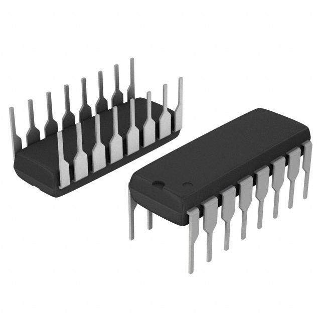
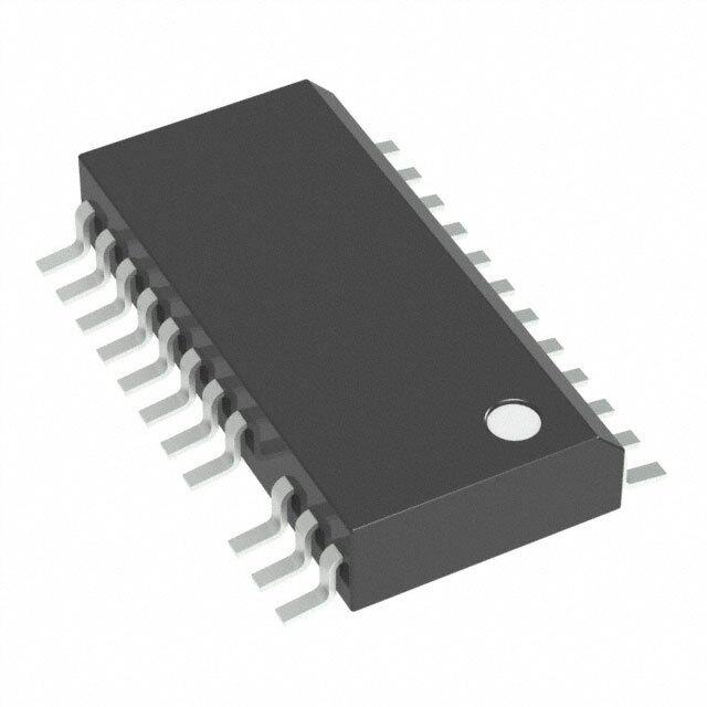
| 供应商器件封装 | 8-SOP |
| 其它名称 | FL6961MYDKR |
| 包装 | Digi-Reel® |
| 单位重量 | 143 mg |
| 商标 | Fairchild Semiconductor |
| 安装类型 | 表面贴装 |
| 安装风格 | SMD/SMT |
| 封装 | Reel |
| 封装/外壳 | 8-SOIC(0.154",3.90mm 宽) |
| 封装/箱体 | SOP-8 |
| 工作温度 | -40°C ~ 125°C |
| 工厂包装数量 | 2500 |
| 开关频率 | 60 kHz |
| 最大功率耗散 | 400 mW |
| 最大工作温度 | + 125 C |
| 最小工作温度 | - 40 C |
| 标准包装 | 1 |
| 模式 | 临界传导(BCM) |
| 特色产品 | http://www.digikey.cn/product-highlights/cn/zh/fairchild-semiconductor-led-solutions/3901 |
| 电压-电源 | 10.5 V ~ 24.5 V |
| 电流-启动 | 10µA |
| 系列 | FL6961 |
| 频率-开关 | - |


- 商务部:美国ITC正式对集成电路等产品启动337调查
- 曝三星4nm工艺存在良率问题 高通将骁龙8 Gen1或转产台积电
- 太阳诱电将投资9.5亿元在常州建新厂生产MLCC 预计2023年完工
- 英特尔发布欧洲新工厂建设计划 深化IDM 2.0 战略
- 台积电先进制程称霸业界 有大客户加持明年业绩稳了
- 达到5530亿美元!SIA预计今年全球半导体销售额将创下新高
- 英特尔拟将自动驾驶子公司Mobileye上市 估值或超500亿美元
- 三星加码芯片和SET,合并消费电子和移动部门,撤换高东真等 CEO
- 三星电子宣布重大人事变动 还合并消费电子和移动部门
- 海关总署:前11个月进口集成电路产品价值2.52万亿元 增长14.8%


PDF Datasheet 数据手册内容提取
Is Now Part of To learn more about ON Semiconductor, please visit our website at www.onsemi.com Please note: As part of the Fairchild Semiconductor integration, some of the Fairchild orderable part numbers will need to change in order to meet ON Semiconductor’s system requirements. Since the ON Semiconductor product management systems do not have the ability to manage part nomenclature that utilizes an underscore (_), the underscore (_) in the Fairchild part numbers will be changed to a dash (-). This document may contain device numbers with an underscore (_). Please check the ON Semiconductor website to verify the updated device numbers. The most current and up-to-date ordering information can be found at www.onsemi.com. Please email any questions regarding the system integration to Fairchild_questions@onsemi.com. ON Semiconductor and the ON Semiconductor logo are trademarks of Semiconductor Components Industries, LLC dba ON Semiconductor or its subsidiaries in the United States and/or other countries. ON Semiconductor owns the rights to a number of patents, trademarks, copyrights, trade secrets, and other intellectual property. A listing of ON Semiconductor’s product/patent coverage may be accessed at www.onsemi.com/site/pdf/Patent-Marking.pdf. ON Semiconductor reserves the right to make changes without further notice to any products herein. ON Semiconductor makes no warranty, representation or guarantee regarding the suitability of its products for any particular purpose, nor does ON Semiconductor assume any liability arising out of the application or use of any product or circuit, and specifically disclaims any and all liability, including without limitation special, consequential or incidental damages. Buyer is responsible for its products and applications using ON Semiconductor products, including compliance with all laws, regulations and safety requirements or standards, regardless of any support or applications information provided by ON Semiconductor. “Typical” parameters which may be provided in ON Semiconductor data sheets and/or specifications can and do vary in different applications and actual performance may vary over time. All operating parameters, including “Typicals” must be validated for each customer application by customer’s technical experts. ON Semiconductor does not convey any license under its patent rights nor the rights of others. ON Semiconductor products are not designed, intended, or authorized for use as a critical component in life support systems or any FDA Class 3 medical devices or medical devices with a same or similar classification in a foreign jurisdiction or any devices intended for implantation in the human body. Should Buyer purchase or use ON Semiconductor products for any such unintended or unauthorized application, Buyer shall indemnify and hold ON Semiconductor and its officers, employees, subsidiaries, affiliates, and distributors harmless against all claims, costs, damages, and expenses, and reasonable attorney fees arising out of, directly or indirectly, any claim of personal injury or death associated with such unintended or unauthorized use, even if such claim alleges that ON Semiconductor was negligent regarding the design or manufacture of the part. ON Semiconductor is an Equal Opportunity/Affirmative Action Employer. This literature is subject to all applicable copyright laws and is not for resale in any manner.
F L 6 9 6 1 January 2012 — S i n g l e - FL6961 S t a Single-Stage Flyback and Boundary Mode PFC g e F Controller for Lighting l y b a c k a n Features d Description B Boundary Mode PFC Controller The FL6961 is a general lighting power controller for ou Low Input Current THD low- to high-power lumens applications requiring power nd factor correction. It is designed for flyback or boost a Controlled On-Time PWM converter operating in Boundary Mode. r y Zero-Current Detection The FL6961 provides a controlled on-time to regulate M the output DC voltage and achieves natural power factor o Cycle-by-Cycle Current Limiting correction (PFC). The maximum on-time of the external d e Leading-Edge Blanking Instead of RC Filtering switch is programmable to ensure safe operation during P Low Startup Current: 10µA Typical AprCo vbidroews nroauptisd. Atrna ninsnieonvta trievesp monusltei- vaenctdo rp ererrcoirs ea mopultipfieurt FC Low Operating Current: 4.5mA Typical voltage clamping. A built-in circuit disables the controller C if the output feedback loop is opened. The startup o Feedback Open-Loop Protection n current is lower than 20µA and the operating current is t r Programmable Maximum On-Time (MOT) less than 6mA. The supply voltage can be up to 25V, o maximizing application flexibility. ll Output Over-Voltage Clamping Protection e r Clamped Gate Output Voltage: 16.5V fo r L Applications i g h General LED Lighting ti n Industrial, Commercial and Residential Fixtures g Outdoor Lighting: Street, Roadway, Parking, Construction, and Ornamental LED Lighting Ordering Information Operating Temperature Part Number Package Packing Method Range FL6961MY -40°C to +125°C 8-Pin, Small Outline Package (SOP) Tape & Reel © 2010 Fairchild Semiconductor Corporation www.fairchildsemi.com FL6961 • Rev. 1.0.2
F L Application Diagram 6 9 6 1 — S i n g l e - S t a g e F l y b a c k Figure 1. Typical Application Circuit for Step-up Converter a n d B o u n d a r y M o d e P F C C o Figure 2. Typical Application Circuit for Single Stage PFC Converter n t r o Block Diagram l l e MOT COMP r f 3 2 o r 2.65V OVP L 2.75V i g h 2.3V t i n 0.45V g INV 1 LEB 4 CS 2.5V SAWTOOTH THD VLIMIT GENERATOR OPTIMIZATION VCC 8 REVGOULTLAAGTOER ISnuteprpnlayl VREF VCC 9R UVLO R Q 1R 2.75V 2.1V/1.75V VZCDHYS = 0.35V ITNIHMIEBRIT S 16.5V 7 GATE VVCCCC__OONFF == 91.25VV DISABLE GND 6 10V 5 ZCD Figure 3. Function Block Diagram © 2010 Fairchild Semiconductor Corporation www.fairchildsemi.com FL6961 • Rev. 1.0.2 2
F Marking Information L 6 9 6 F- Fairchild Logo 1 — Z- Plant Code S X- Year Code i n Y- Week Code g l FL6961 TT: Die Run Code e TPM -S T: Package Type (M=SOP) t a P: Z: Pb Free Y: Green Compound g e M: Manufacture Flow Code F l y b a c Figure 4. Marking Information k a n Pin Configuration d B o u n d a r y M o d e P F C C o n Figure 5. Pin Configuration (Top View) tr o l l e r f o Pin Definitions r L i g Pin # Name Description h t i Inverting Input of the Error Amplifier. INV is connected to the converter output via a resistive n 1 INV g divider. This pin is also used for over-voltage clamping and open-loop feedback protection. Output of the Error Amplifier. To create a precise clamping protection, a compensation network 2 COMP between this pin and GND is suggested. Maximum On Time. A resistor from MOT to GND is used to determine the maximum on-time of 3 MOT the external power MOSFET. The maximum output power of the converter is a function of the maximum on-time. Current Sense. Input to the over-current protection comparator. When the sensed voltage across 4 CS the sense resistor reaches the internal threshold (0.8V), the switch is turned off to activate cycle- by-cycle current limiting. Zero-Current Detection. This pin is connected to an auxiliary winding via a resistor to detect the 5 ZCD zero crossing of the switch current. When the zero crossing is detected, a new switching cycle is started. If it is connected to GND, the device is disabled. Ground. The power ground and signal ground. Placing a 0.1µF decoupling capacitor between 6 GND V and GND is recommended. CC Driver Output. Totem-pole driver output to drive the external power MOSFET. The clamped gate 7 GATE output voltage is 16.5V. 8 V Power Supply. Driver and control circuit supply voltage. CC © 2010 Fairchild Semiconductor Corporation www.fairchildsemi.com FL6961 • Rev. 1.0.2 3
F L Absolute Maximum Ratings 6 9 6 Stresses exceeding the absolute maximum ratings may damage the device. The device may not function or be 1 operable above the recommended operating conditions and stressing the parts to these levels is not recommended. — In addition, extended exposure to stresses above the recommended operating conditions may affect device reliability. S The absolute maximum ratings are stress ratings only. All voltage values, except differential voltage, are given with i respect to GND pin. n g l Symbol Parameter Min. Max. Unit e - S VVCC DC Supply Voltage 30 V t a V Gate Driver -0.3 30.0 V g HIGH e VLOW Others (INV, COMP, MOT, CS) -0.3 7.0 V F l y V Input Voltage to ZCD Pin -0.3 12.0 V ZCD b a PD Power Dissipation 660 mW c k TJ Operating Junction Temperature -40 +150 C a n θJA Thermal Resistance (Junction-to-Air) 150 C/W d θ Thermal Resistance (Junction-to-Case) 39 C/W B JC o T Storage Temperature Range -65 +150 C u STG n T Lead Temperature (Wave Soldering or IR, 10 Seconds) +230 C d L a r Human Body Model: JESD22-A114 2.5 KV y ESD M Machine Model: JESD22-A115 200 V o d e P F C Recommended Operating Conditions C o The Recommended Operating Conditions table defines the conditions for actual device operation. Recommended n operating conditions are specified to ensure optimal performance to the datasheet specifications. Fairchild does not t r recommend exceeding them or designing to Absolute Maximum Ratings. o l l e Symbol Parameter Min. Typ. Max. Unit r f T Operating Ambient Temperature -40 +125 C o A r L i g h t i n g © 2010 Fairchild Semiconductor Corporation www.fairchildsemi.com FL6961 • Rev. 1.0.2 4
F L 6 9 Electrical Characteristics 6 1 Unless otherwise noted, V =15V and T =-40°C to 150°C. Current is defined as positive into the device and negative — CC J out of the device. S i Symbol Parameter Conditions Min. Typ. Max. Units n g l V Section e CC - S V Continuous Operation Voltage 24.5 V t CC-OP a g VCC-ON Turn-On Threshold Voltage 11.5 12.5 13.5 V e F VCC-OFF Turn-Off Threshold Voltage 8.5 9.5 10.5 V ly b ICC-ST Startup Current VCC=VCC-ON – 0.16V 10 20 µA a c V =12V, V =0V, k ICC-OP Operating Supply Current CC=C3nF, f C=S60KHz 4.5 6 mA a L SW n d V V Over-Voltage Protection Level 26.8 27.8 28.8 V CC-OVP DD B t V Over-Voltage Protection Debounce 30 µs o D-VCCOVP DD u n Error Amplifier Section d a VREF Reference Voltage 2.475 2.500 2.525 V ry Gm Transconductance 125 μmho M o V Clamp High Feedback Voltage 2.65 2.70 V d INVH e V Clamp Low Feedback Voltage 2.25 2.30 V P INVL F V Output High Voltage 4.8 V C OUT HIGH C VOZ Zero Duty Cycle Output Voltage 1.15 1.25 1.35 V o n V Over-Voltage Protection for INV Input 2.70 2.75 2.80 V t INV-OVP r o VINV-UVP Under-Voltage Protection for INV Input 0.40 0.45 0.50 V lle r V =2.35V, V =1.5V 10 20 INV COMP f Source Current o ICOMP VINV=1.5V 550 800 μA r L i Sink Current V =2.65V, V =5V 10 20 g INV COMP h Current-Sense Section ti n g VPK TChyrceles-hboyl-dC Vyoclleta Lgiem fiot r Peak Current Limit 0.77 0.82 0.87 V t Propagation Delay 200 ns PD R =24kΩ, V =5V 400 500 MOT COMP t Leading-Edge Blanking Time ns LEB R =24kΩ, MOT 270 350 V =V +50mV COMP OZ Gate Section V - Output Voltage Maximum (Clamp) V =25V 14.5 16.0 17.5 V ZOUT CC V Output Voltage Low V =15V, I =100mA 1.4 V OL CC O V Output Voltage High V =14V, I =100mA 8 V OH CC O V =12V, C =3nF, t Rising Time CC L 80 ns R 20~80% V =12V, C =3nF, t Falling Time CC L 40 ns F 80~20% Continued on the following page… © 2010 Fairchild Semiconductor Corporation www.fairchildsemi.com FL6961 • Rev. 1.0.2 5
F L 6 Electrical Characteristics 9 6 1 Unless otherwise noted, VCC=15V and TJ=-40°C to 150°C. Current is defined as positive into the device and negative — out of the device. S Symbol Parameter Conditions Min. Typ. Max. Units in g Zero-Current Detection Section le - S V Input Threshold Voltage Rising Edge V Increasing 1.9 2.1 2.3 V ZCD ZCD t a H of g YS Threshold Voltage Hysteresis V Decreasing 0.35 V e VZCD ZCD F l V Upper Clamp Voltage I =3mA 12 V y ZCD-HIGH ZCD b a VZCD-LOW Lower Clamp Voltage IZCD=-1.5mA 0.3 V c k t Maximum Delay, ZCD to Output Turn-On VCOMP=5V, 100 400 ns a DEAD f =60KHz n SW d Output Turned Off by B tRESTART Restart Time ZCD 300 500 700 μs o u n t Inhibit Time (Maximum Switching R =24kΩ 2.8 μs d INHIB Frequency Limit) MOT a r y VDIS Disable Threshold Voltage 130 200 250 mV M R =24kΩ, o t Disable Function Debounce Time MOT 800 μs d ZCD-DIS VZCD=100mV e P Maximum On Time Section F C VMOT Maximum On Time Voltage 1.25 1.30 1.35 V C o Maximum On Time Programming R =24kΩ, V =0V, t MOT CS 25 μs n ON-MAX (Resistor Based) VCOMP=5V tr o l l e r f o r L i g h t i n g © 2010 Fairchild Semiconductor Corporation www.fairchildsemi.com FL6961 • Rev. 1.0.2 6
F L 6 9 Typical Performance Characteristics 6 1 — S 2.525 3.0 i n g l 2.515 2.4 e - S ) A t 2.505 m1.8 a V(V)ref 2.495 (CC-OP 1.2 ge Fly I b 2.485 0.6 a c k 2.475 0.0 a -40 -25 -10 5 20 35 50 65 80 95 110 125 -40 -25 -10 5 20 35 50 65 80 95 110 125 n d Temperature (℃) Temperature (℃) B o u n Figure 6. V vs. T Figure 7. I vs. T d REF A CC-OP A a r y M 24.60 14.0 o d e 24.52 13.4 P s) F (μ 24.44 V) 12.8 C MAX 24.36 (ON Co N- h-12.2 n O Vt t t r 24.28 o 11.6 ll e 24.20 r f -40 -25 -10 5 20 35 50 65 80 95 110 125 11.0 o -40 -25 -10 5 20 35 50 65 80 95 110 125 r L Temperature (℃) Temperature (℃) ig h t i n Figure 8. t vs. T Figure 9. V vs. T g ON-MAX A th-ON A 10.5 16.0 10.1 13.6 ) ) V A ( 9.7 μ11.2 OFF (ST Vth- 9.3 CC- 8.8 I 8.9 6.4 8.5 4.0 -40 -25 -10 5 20 35 50 65 80 95 110 125 -40 -25 -10 5 20 35 50 65 80 95 110 125 Temperature (℃) Temperature (℃) Figure 10. V vs. T Figure 11.I vs. T th-OFF A CC-ST A © 2010 Fairchild Semiconductor Corporation www.fairchildsemi.com FL6961 • Rev. 1.0.2 7
F L 6 9 Typical Performance Characteristics (Continued) 6 1 — S 1.350 18.0 i n g l 1.330 17.4 e - S V)1.310 V)16.8 ta V(MOT 1.290 V(Z-OUT 16.2 ge Fly b 1.270 15.6 a c k 1.250 15.0 a n -40 -25 -10 5 20 35 50 65 80 95 110 125 -40 -25 -10 5 20 35 50 65 80 95 110 125 d Temperature (℃) Temperature (℃) B o u n Figure 12. V vs. T Figure 13.V vs. T d MOT A Z-OUT A a r y 0.87 M o 0.85 d e P V)0.83 F ( C VPK 0.81 Co n t 0.79 r o l l e 0.77 r -40 -25 -10 5 20 35 50 65 80 95 110 125 fo r Temperature (℃) L i g h Figure 14. VPK vs. TA tin g © 2010 Fairchild Semiconductor Corporation www.fairchildsemi.com FL6961 • Rev. 1.0.2 8
F L Functional Description 6 9 6 1 Error Amplifier Leading-Edge Blanking (LEB) — The inverting input of the error amplifier is referenced to A turn-on spike on the CS pin appears when the power S INV. The output of the error amplifier is referenced to MOSFET is switched on. At the beginning of each i COMP. The non-inverting input is internally connected switching pulse, the current-limit comparator is disabled n g to a fixed 2.5V ±2% voltage. The output of the error for around 400ns to avoid premature termination. The l e amplifier is used to determine the on-time of the PWM gate drive output cannot be switched off during the - S output and regulate the output voltage. To achieve a blanking period. Conventional RC filtering is not t a low input current THD, the variation of the on-time necessary, so the propagation delay of current limit g within one input AC cycle should be very small. A multi- protection can be minimized. e vector error amplifier is built in to provide fast transient F Under-Voltage Lockout (UVLO) l response and precise output voltage clamping. y b The turn-on and turn-off threshold voltages are fixed Connecting a capacitance, such as 1µF, between a internally at 12V and 9.5V, respectively. This hysteresis c COMP and GND is suggested. The error amplifier is a behavior guarantees a one-shot startup with proper k trans-conductance amplifier that converts voltage to a startup resistor and hold-up capacitor. With an ultra-low current with a 125µmho. n startup current of 20µA, one 1MΩ R is sufficient for d IN Startup Current startup under low input line voltage, 85Vrms. Power B dissipation on R would be less than 0.1W even under o Typical startup current is less than 20µA. This ultra-low IN u high line (V =265V ) condition. startup current allows the usage of a high resistance, AC rms n d low-wattage startup resistor. For example, 1MΩ/0.25W Output Driver a startup resistor and a 10µF/25V (V hold-up) capacitor r CC With low on resistance and high current driving y are recommended for an AC-to-DC power adaptor with capability, the output driver can drive an external M a wide input range 85-265VAC. capacitive load larger than 3000pF. Cross conduction o d Operating Current current has been avoided to minimize heat dissipation, e improving efficiency and reliability. This output driver is P Operating current is typically 4.5mA. The low operating internally clamped by a 16.5V Zener diode. F current enables better efficiency and reduces the C requirement of VCC hold-up capacitance. Zero-Current Detection (ZCD) C o Maximum On-Time Operation The zero-current detection of the inductor is achieved n using its auxiliary winding. When the stored energy of t Given a fixed inductor value and maximum output r the inductor is fully released to output, the voltage on o power, the relationship between on-time and line l ZCD goes down and a new switching cycle is enabled le voltage is: after a ZCD trigger. The power MOSFET is always r f 2LP turned on with zero inductor current such that turn-on o tonV 2o (1) loss and noise can be minimized. The converter works r L rms in Boundary Mode and peak inductor current is always i g If the line voltage is too low or the inductor value is too exactly twice of the average current. A natural power h high, tON is too long. To avoid extra low operating factor correction function is achieved with the low- tin frequency and achieve brownout protection, the bandwidth, on-time modulation. An inherent maximum g maximum value of tON is programmable by one resistor, off time is built in to ensure proper startup operation. R, connected between MOT and GND. A 24kΩ resistor This ZCD pin can be used as a synchronous input. I R generates corresponds to 25µs maximum on time: I Noise Immunity ton(max) RI(k)25s (2) Nsigonisiefic oann tt hpeu clsuer-rwenidt tshe njisttee ro, r pcaorntitcruolla srilgy nainl cBaonu cnaduasrey 24 Mode. Slope compensation and a built-in debounce The range of the maximum on-time is 10 ~ 50µs. circuit can alleviate this problem. Because the FL6961 has a single ground pin, high sink current at the output Peak Current Limiting cannot be returned separately. Good high-frequency or The switch current is sensed by one resistor. The signal RF layout practices should be followed. Avoiding long is fed into the CS pin and an input terminal of a PCB traces and component leads, locating comparator. A high voltage on the CS pin terminates compensation and filter components near to the the switching cycle immediately and cycle-by-cycle FL6961, and increasing the power MOSFET gate current limit is achieved. The designed threshold of the resistance all improve performance. protection point is 0.82V. © 2010 Fairchild Semiconductor Corporation www.fairchildsemi.com FL6961 • Rev. 1.0.2 9
F Physical Dimensions L 6 9 6 5.00 1 4.80 — A 0.65 S i 3.81 n g l 8 5 e B -S t a g 6.20 1.75 e 5.80 4.00 5.60 F l 3.80 y b a c k a 1 4 n PIN ONE d INDICATOR 1.27 B 1.27 o (0.33) u 0.25 M C B A n LAND PATTERN RECOMMENDATION d a r y M 0.25 SEE DETAIL A o d 0.10 e 0.25 P F 1.75 MAX C 0.19 C C 0.51 0.10 C o n 0.33 OPTION A - BEVEL EDGE t r o 0.50 x 45° ll 0.25 e R0.10 GAGE PLANE r f o R0.10 OPTION B - NO BEVEL EDGE r 0.36 L i g 8° NOTES: UNLESS OTHERWISE SPECIFIED h t i 0° n A) THIS PACKAGE CONFORMS TO JEDEC g 0.90 MS-012, VARIATION AA, ISSUE C, SEATING PLANE B) ALL DIMENSIONS ARE IN MILLIMETERS. 0.406 (1.04) C) DIMENSIONS DO NOT INCLUDE MOLD FLASH OR BURRS. DETAIL A D) LANDPATTERN STANDARD: SOIC127P600X175-8M. SCALE: 2:1 E) DRAWING FILENAME: M08AREV13 Figure 15. 8-Lead, SOIC, JEDEC MS-012, .150 Inch Narrow Body Package drawings are provided as a service to customers considering Fairchild components. Drawings may change in any manner without notice. Please note the revision and/or date on the drawing and contact a Fairchild Semiconductor representative to verify or obtain the most recent revision. Package specifications do not expand the terms of Fairchild’s worldwide terms and conditions, specifically the warranty therein, which covers Fairchild products. Always visit Fairchild Semiconductor’s online packaging area for the most recent package drawings: http://www.fairchildsemi.com/packaging/. © 2010 Fairchild Semiconductor Corporation www.fairchildsemi.com FL6961 • Rev. 1.0.2 10
F L 6 9 6 1 — S i n g l e - S t a g e F l y b a c k a n d B o u n d a r y M o d e P F C C o n t r o l l e r f o r L i g h t i n g © 2010 Fairchild Semiconductor Corporation www.fairchildsemi.com FL6961 • Rev. 1.0.2 11
ON Semiconductor and are trademarks of Semiconductor Components Industries, LLC dba ON Semiconductor or its subsidiaries in the United States and/or other countries. ON Semiconductor owns the rights to a number of patents, trademarks, copyrights, trade secrets, and other intellectual property. A listing of ON Semiconductor’s product/patent coverage may be accessed at www.onsemi.com/site/pdf/Patent−Marking.pdf. ON Semiconductor reserves the right to make changes without further notice to any products herein. ON Semiconductor makes no warranty, representation or guarantee regarding the suitability of its products for any particular purpose, nor does ON Semiconductor assume any liability arising out of the application or use of any product or circuit, and specifically disclaims any and all liability, including without limitation special, consequential or incidental damages. Buyer is responsible for its products and applications using ON Semiconductor products, including compliance with all laws, regulations and safety requirements or standards, regardless of any support or applications information provided by ON Semiconductor. “Typical” parameters which may be provided in ON Semiconductor data sheets and/or specifications can and do vary in different applications and actual performance may vary over time. All operating parameters, including “Typicals” must be validated for each customer application by customer’s technical experts. ON Semiconductor does not convey any license under its patent rights nor the rights of others. ON Semiconductor products are not designed, intended, or authorized for use as a critical component in life support systems or any FDA Class 3 medical devices or medical devices with a same or similar classification in a foreign jurisdiction or any devices intended for implantation in the human body. Should Buyer purchase or use ON Semiconductor products for any such unintended or unauthorized application, Buyer shall indemnify and hold ON Semiconductor and its officers, employees, subsidiaries, affiliates, and distributors harmless against all claims, costs, damages, and expenses, and reasonable attorney fees arising out of, directly or indirectly, any claim of personal injury or death associated with such unintended or unauthorized use, even if such claim alleges that ON Semiconductor was negligent regarding the design or manufacture of the part. ON Semiconductor is an Equal Opportunity/Affirmative Action Employer. This literature is subject to all applicable copyright laws and is not for resale in any manner. PUBLICATION ORDERING INFORMATION LITERATURE FULFILLMENT: N. American Technical Support: 800−282−9855 Toll Free ON Semiconductor Website: www.onsemi.com Literature Distribution Center for ON Semiconductor USA/Canada 19521 E. 32nd Pkwy, Aurora, Colorado 80011 USA Europe, Middle East and Africa Technical Support: Order Literature: http://www.onsemi.com/orderlit Phone: 303−675−2175 or 800−344−3860 Toll Free USA/Canada Phone: 421 33 790 2910 Fax: 303−675−2176 or 800−344−3867 Toll Free USA/Canada Japan Customer Focus Center For additional information, please contact your local Email: orderlit@onsemi.com Phone: 81−3−5817−1050 Sales Representative © Semiconductor Components Industries, LLC www.onsemi.com www.onsemi.com 1