ICGOO在线商城 > UC232R-10-NE
/UC232R-10-NE.jpg)
 Datasheet下载
- 型号: UC232R-10-NE
- 制造商: FTDI
- 库位|库存: xxxx|xxxx
- 要求:
| 数量阶梯 | 香港交货 | 国内含税 |
| +xxxx | $xxxx | ¥xxxx |
查看当月历史价格
查看今年历史价格
UC232R-10-NE产品简介:
ICGOO电子元器件商城为您提供UC232R-10-NE由FTDI设计生产,在icgoo商城现货销售,并且可以通过原厂、代理商等渠道进行代购。 提供UC232R-10-NE价格参考以及FTDIUC232R-10-NE封装/规格参数等产品信息。 你可以下载UC232R-10-NE参考资料、Datasheet数据手册功能说明书, 资料中有UC232R-10-NE详细功能的应用电路图电压和使用方法及教程。
| 参数 | 数值 |
| 产品目录 | |
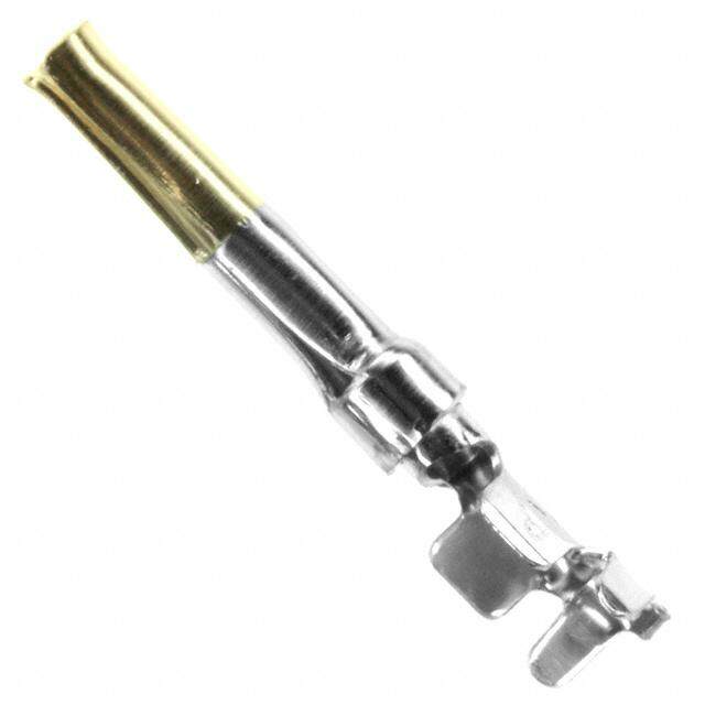
| 描述 | CABLE USB RS232 NO ENCLOSRE 10CMUSB数据线/IEEE 1394数据线 USB to RS232 Embeded Conv, Open PCB 10cm |
| 产品分类 | |
| 品牌 | FTDI |
| 产品手册 | |
| 产品图片 |
|
| rohs | 符合RoHS无铅 / 符合限制有害物质指令(RoHS)规范要求 |
| 产品系列 | USB数据线/IEEE 1394数据线,FTDI UC232R-10-NEUC232R |
| 数据手册 | |
| 产品型号 | UC232R-10-NE |
| 产品 | USB Cables |
| 产品种类 | USB数据线/IEEE 1394数据线 |
| 使用 | USB 至 RS232 |
| 其它名称 | 768-1073 |
| 商标 | FTDI |
| 型式 | Male / Male |
| 导体数量 | 9 |
| 封装 | Bulk |
| 屏蔽 | - |
| 工厂包装数量 | 100 |
| 描述/功能 | USB to Serial Cable Assembly |
| 标准包装 | 10 |
| 类型 | Evaluation Cable |
| 线规-美国线规(AWG) | 24 |
| 转换自(适配器端) | USB - A,插头 |
| 转换至(适配器端) | D-Sub,9 公型引脚 |
| 连接器端口A | USB Type A |
| 连接器端口A管脚计数 | 4 |
| 连接器端口B | DB9 |
| 连接器端口B管脚计数 | 9 |
| 长度 | 10 cm |
| 颜色 | White |


- 商务部:美国ITC正式对集成电路等产品启动337调查
- 曝三星4nm工艺存在良率问题 高通将骁龙8 Gen1或转产台积电
- 太阳诱电将投资9.5亿元在常州建新厂生产MLCC 预计2023年完工
- 英特尔发布欧洲新工厂建设计划 深化IDM 2.0 战略
- 台积电先进制程称霸业界 有大客户加持明年业绩稳了
- 达到5530亿美元!SIA预计今年全球半导体销售额将创下新高
- 英特尔拟将自动驾驶子公司Mobileye上市 估值或超500亿美元
- 三星加码芯片和SET,合并消费电子和移动部门,撤换高东真等 CEO
- 三星电子宣布重大人事变动 还合并消费电子和移动部门
- 海关总署:前11个月进口集成电路产品价值2.52万亿元 增长14.8%


PDF Datasheet 数据手册内容提取
™ Future Technology Devices International Ltd. UC232R “ChiPi” Minimum Component FT232RL USB to RS232 Converter Cable Incorporating Clock Generator Output and FTDIChip-ID™ Security Dongle The UC232R “ChiPi” is a USB to RS232 converter cable incorporating FTDI’s FT232RL USB - Serial UART interface IC device, the latest device to be added to FTDI’s range of USB UART interface Integrated Circuit Devices. It has been designed to use the minimum number of The FT232RL is a USB to serial UART interface with optional clock generator output, and the new FTDIChip-ID™ security dongle feature. In addition, asynchronous and synchronous bit bang interface modes are available. USB to serial interface designs using the FT232RL have been further simplifi ed by fully integrating the external EEPROM, clock circuit and USB resistors onto the device. The FT232RL adds two new functions compared with its predecessors, effectively making it a “3-in-1” chip for some application areas. The internally generated clock (6MHz, 12MHz, 24MHz, and 48MHz) can be brought out of the device and used to drive a microcontroller or external logic. A unique number (the FTDIChip-ID™) is burnt into the device during manufacture and is readable over USB, thus forming the basis of a security dongle which can be used to protect customer application software from being copied. The UC232R is supplied on a 16.2 mm x 41.3mm (0.6” x 1.6”) PCB, including the DB9 connector. A 295mm (11.8”) USB cable with USB ‘A’ plug is fi tted. All components used, including the FT232RL and RS232 level converter IC are Pb-free (RoHS compliant). Copyright © Future Technology Devices International Ltd. 2005
Page 2 1. Features 1.1 Hardware Features • UC232R Converter Cable provides USB to RS232 • Device supplied preprogrammed with unique USB (DB9) interface. serial number. • FCC and CE Class B Approval • Support for USB suspend and resume. • Full design files available from FTDI website. • Converter cable supply voltage comes from VCC • FT232RL provides single chip USB to - no external supply required. asynchronous serial data transfer interface. • FT232RL has integrated USB resistors. • Entire USB protocol handled on the FT232RL chip • Integrated power-on-reset circuit in FT232RL IC - No USB-specific firmware programming required. device. • UART interface support for 7 or 8 data bits, 1 or 2 • Fully integrated clock in FT232RL - no external stop bits and odd / even / mark / space / no parity. crystal, oscillator, or resonator required. • Fully assisted hardware or X-On / X-Off software • FT232RL has fully integrated AVCC supply filtering handshaking. - No separate AVCC pin and no external R-C filter • Data transfer rates from 300 baud to 250 kilobaud required. at RS232 levels. • USB bulk transfer mode. • FTDI’s royalty-free VCP and D2XX drivers • Low operating and USB suspend current. eliminate the requirement for USB driver • Low USB bandwidth consumption. development in most cases. • UHCI / OHCI / EHCI host controller compatible • In-built support for event characters and line break • USB 2.0 Full Speed compatible. condition. • -40°C to 85°C extended operating temperature • New USB FTDIChip-ID™ feature. range. • FIFO receive and transmit buffers for high data • Supplied on 16.2 mm x 41.3mm (0.6” x 1.6”) throughput. 61.0mm x 32.0mm (2.40” x 1.26”) PCB, including • Adjustable receive buffer timeout. DB9 RS232 connector. • Integrated 1024 bit internal EEPROM for storing • Connect to a PC via standard USB ‘A’ plug on USB VID, PID, serial number and product 30cm USB cable. description strings. 1.2 Driver Support Royalty-Free VIRTUAL COM PORT Royalty-Free D2XX Direct Drivers (VCP) DRIVERS for... (USB Drivers + DLL S/W Interface) • Windows 98, 98SE, ME, 2000, Server 2003, XP. • Windows 98, 98SE, ME, 2000, Server 2003, XP. • Windows Vista / Longhorn* • Windows Vista / Longhorn* • Windows XP 64-bit.* • Windows XP 64-bit.* • Windows XP Embedded. • Windows XP Embedded. • Windows CE.NET 4.2 & 5.0 • Windows CE.NET 4.2 & 5.0 • MAC OS 8 / 9, OS-X • Linux 2.4 and greater • Linux 2.4 and greater The drivers listed above are all available to download for free from the FTDI website. Various 3rd Party Drivers are also available for various other operating systems - see the FTDI website for details. * Currently Under Development. Contact FTDI for availability. 1.3 Typical Applications • USB to RS232 Converter • USB FLASH Card Reader / Writers • Upgrading Legacy Peripherals to USB • Set Top Box PC - USB interface • USB Audio and Low Bandwidth Video data transfer • USB Digital Camera Interface • PDA to USB data transfer • USB Hardware Modems • USB Smart Card Readers • USB Wireless Modems • USB Instrumentation • USB Bar Code Readers • USB Industrial Control • USB Software / Hardware Encryption Dongles • USB MP3 Player Interface UC232R “ChiPi” Minimum Component FT232RL USB to RS232 Converter Cable Datasheet Version 0.90 © Future Technology Devices International Ltd. 2005
Page 3 2. Features and Enhancements of FT232R 2.1 FT232R Key Features This section summarises the key features and enhancements of the FT232R IC device which is used on the UC232R “ChiPi” USB to RS232 converter cable. For further details, consult the FT232R datasheet, which is available from the FTDI website. Integrated Clock Circuit - Previous generations of FTDI’s USB UART devices required an external crystal or ceramic resonator. The clock circuit has now been integrated onto the device meaning that no crystal or ceramic resonator is required. However, if required, an external 12MHz crystal can be used as the clock source. Integrated EEPROM - Previous generations of FTDI’s USB UART devices required an external EEPROM if the device were to use USB Vendor ID (VID), Product ID (PID), serial number and product description strings other than the default values in the device itself. This external EEPROM has now been integrated onto the FT232R chip meaning that all designs have the option to change the product description strings. A user area of the internal EEPROM is available for storing additional data. The internal EEPROM is programmable in circuit, over USB without any additional voltage requirement. Preprogrammed EEPROM - The FT232R is supplied with its internal EEPROM preprogrammed with a serial number which is unique to each individual device. This, in most cases, will remove the need to program the device EEPROM. Integrated USB Resistors - Previous generations of FTDI’s USB UART devices required two external series resistors on the USBDP and USBDM lines, and a 1.5 kΩ pull up resistor on USBDP. These three resistors have now been integrated onto the device. Integrated AVCC Filtering - Previous generations of FTDI’s USB UART devices had a separate AVCC pin - the supply to the internal PLL. This pin required an external R-C filter. The separate AVCC pin is now connected internally to VCC, and the filter has now been integrated onto the chip. Less External Components - Integration of the crystal, EEPROM, USB resistors, and AVCC filter will substantially reduce the bill of materials cost for USB interface designs using the FT232R compared to its FT232BM predecessor. Configurable CBUS I/O Pin Options - There are now 5 configurable Control Bus (CBUS) lines. Options are TXDEN - transmit enable for RS485 designs, PWREN# - Power control for high power, bus powered designs, TXLED# - for pulsing an LED upon transmission of data, RXLED# - for pulsing an LED upon receiving data, TX&RXLED# - which will pulse an LED upon transmission OR reception of data, SLEEP# - indicates that the device going into USB suspend mode, CLK48 / CLK24 / CLK12 / CLK6 - 48MHz, 24MHz,12MHz, and 6MHz clock output signal options. There is also the option to bring out bit bang mode read and write strobes (see below). The CBUS lines can be configured with any one of these output options by setting bits in the internal EEPROM. The device is supplied with the most commonly used pin definitions preprogrammed - see Section 8 for details. Enhanced Asynchronous Bit Bang Mode with RD# and WR# Strobes - The FT232R supports FTDI’s BM chip bit bang mode. In bit bang mode, the eight UART lines can be switched from the regular interface mode to an 8-bit general purpose I/O port. Data packets can be sent to the device and they will be sequentially sent to the interface at a rate controlled by an internal timer (equivalent to the baud rate prescaler). With the FT232R device this mode has been enhanced so that the internal RD# and WR# strobes are now brought out of the device which can be used to allow external logic to be clocked by accesses to the bit bang I/O bus. This option will be described more fully in a separate application note. Synchronous Bit Bang Mode - Synchronous bit bang mode differs from asynchronous bit bang mode in that the interface pins are only read when the device is written to. Thus making it easier for the controlling program to measure the response to an output stimulus as the data returned is synchronous to the output data. The feature was previously seen in FTDI’s FT2232C device. This option will be described more fully in a separate application note. CBUS Bit Bang Mode - This mode allows four of the CBUS pins to be individually configured as GPIO pins, similar to Asynchronous bit bang mode. It is possible to use this mode while the UART interface is being used, thus providing up to four general purpose I/O pins which are available during normal operation. An application note describing this feature is available separately from the FTDI website. UC232R “ChiPi” Minimum Component FT232RL USB to RS232 Converter Cable Datasheet Version 0.90 © Future Technology Devices International Ltd. 2005
Page 4 Lower Supply Voltage - Previous generations of the chip required 5V supply on the VCC pin. The FT232R will work with a Vcc supply in the range 3.3V - 5.25V. Bus powered designs would still take their supply from the 5V on the USB bus, but for self powered designs where only 3.3V is available and there is no 5V supply there is no longer any need for an additional external regulator. Integrated Level Converter on UART Interface and Control Signals - VCCIO pin supply can be from 1.8V to 5V. Connecting the VCCIO pin to 1.8V, 2.8V, or 3.3V allows the device to directly interface to 1.8V, 2.8V or 3.3V and other logic families without the need for external level converter I.C. devices. 5V / 3.3V / 2.8V / 1.8V Logic Interface - The FT232R provides true CMOS Drive Outputs and TTL level Inputs. Integrated Power-On-Reset (POR) Circuit- The device incorporates an internal POR function. A RESET# pin is available in order to allow external logic to reset the FT232R where required. However, for many applications the RESET# pin can be left unconnected, or pulled up to VCCIO. Lower Operating and Suspend Current - The device operating supply current has been further reduced to 15mA, and the suspend current has been reduced to around 70μA. This allows greater margin for peripheral designs to meet the USB suspend current limit of 500μA. Low USB Bandwidth Consumption - The operation of the USB interface to the FT232R has been designed to use as little as possible of the total USB bandwidth available from the USB host controller. High Output Drive Option - The UART interface and CBUS I/O pins can be made to drive out at three times the standard signal drive level thus allowing multiple devices to be driven, or devices that require a greater signal drive strength to be interfaced to the FT232R. This option is enabled in the internal EEPROM. Power Management Control for USB Bus Powered, High Current Designs- The PWREN# signal can be used to directly drive a transistor or P-Channel MOSFET in applications where power switching of external circuitry is required. An option in the internal EEPROM makes the device gently pull down on its UART interface lines when the power is shut off (PWREN# is high). In this mode any residual voltage on external circuitry is bled to GND when power is removed, thus ensuring that external circuitry controlled by PWREN# resets reliably when power is restored. UART Pin Signal Inversion - The sense of each of the eight UART signals can be individually inverted by setting options in the internal EEPROM. Thus, CTS# (active low) can be changed to CTS (active high), or TXD can be changed to TXD#. FTDIChip-ID™ - Each FT232R is assigned a unique number which is burnt into the device at manufacture. This ID number cannot be reprogrammed by product manufacturers or end-users. This allows the possibility of using FT232R based dongles for software licensing. Further to this, a renewable license scheme can be implemented based on the FTDIChip-ID™ number when encrypted with other information. This encrypted number can be stored in the user area of the FT232R internal EEPROM, and can be decrypted, then compared with the protected FTDIChip-ID™ to verify that a license is valid. Web based applications can be used to maintain product licensing this way. An application note describing this feature is available separately from the FTDI website. Improved EMI Performance - The reduced operating current and improved on-chip VCC decoupling significantly improves the ease of PCB design requirements in order to meet FCC, CE and other EMI related specifications. Programmable Receive Buffer Timeout - The receive buffer timeout is used to flush remaining data from the receive buffer. This time defaults to 16ms, but is programmable over USB in 1ms increments from 1ms to 255ms, thus allowing the device to be optimised for protocols that require fast response times from short data packets. Baud Rates - The FT232R supports all standard baud rates and non-standard baud rates from 300 Baud up to 3 Megabaud. Achievable non-standard baud rates are calculated as follows - Baud Rate = 3000000 / (n + x) where n can be any integer between 2 and 16,384 ( = 214 ) and x can be a sub-integer of the value 0, 0.125, 0.25, 0.375, 0.5, 0.625, 0.75, or 0.875. When n = 1, x = 0, i.e. baud rate divisors with values between 1 and 2 are not possible. This gives achievable baud rates in the range 183.1 baud to 3,000,000 baud. When a non-standard baud rate is required simply pass the required baud rate value to the driver as normal, and the FTDI driver will calculate the required divisor, and set the baud rate. See FTDI application note AN232B-05 for more details. UC232R “ChiPi” Minimum Component FT232RL USB to RS232 Converter Cable Datasheet Version 0.90 © Future Technology Devices International Ltd. 2005
Page 5 Extended Operating Temperature Range - The FT232R operates over an extended temperature range of -40º to +85º C thus allowing the device to be used in automotive and industrial applications. New Package Options - The FT232R is available in two packages - a compact 28 pin SSOP ( FT232RL) and an ultra-compact 5mm x 5mm pinless QFN-32 package ( FT232RQ). Both packages are lead ( Pb ) free, and use a ‘green’ compound. Both packages are fully compliant with European Union directive 2002/95/EC. The MM232R module uses a FT232RQ device in its design. Figure 1 - The UC232R “ChiPi” USB to RS232 Converter Cable. UC232R “ChiPi” Minimum Component FT232RL USB to RS232 Converter Cable Datasheet Version 0.90 © Future Technology Devices International Ltd. 2005
Page 6 3. UC232R Pin Out and Signal Descriptions 3.1 UC232R Pin Out DCD RXD TXD DTR GND 1 2 3 4 5 DSR RTS CTS RI 6 7 8 9 Figure 2 - UC232R RS232 (DB9) Pin Out 3.2 RS232 Signal Descriptions Table 1 - RS232 Signals DB9 pin No. Name Type Description 1 DCD Input Data Carrier Detect control input 2 RXDATA Input Receive Asynchronous Data input. 3 TXDATA Output Transmit Asynchronous Data output. 4 DTR Output Data Terminal Ready control output / Handshake signal 5 GND GND Device groud supply pin. 6 DSR Input Data Set Ready control input / Handshake signal 7 RTS Output Request To Send Control Output / Handshake signal. 8 CTS Input Clear to Send Control input / Handshake signal. 9 RI Input Ring Indicator control input. When remote wakeup is enabled in the FT232RL’s internal EEPROM taking RI# low can be used to resume the PC USB host controller from suspend. UC232R “ChiPi” Minimum Component FT232RL USB to RS232 Converter Cable Datasheet Version 0.90 © Future Technology Devices International Ltd. 2005
Page 7 4. UC232R Dimensions 41.30mm (1.63") 16.20mm 18mm 30.90mm (0.64") F TDI (0.71") (1.22") 29.30mm (1.15") 3.90mm (0.15") 6.00mm (0.24") 1.70mm 9.10mm 12.55mm (0.07") (0.36") (0.50") 11.00mm (0.44") Figure 3 - UC232R “ChiPi” USB to RS232 Converter Dimensions All dimensions are stated in millimeters, with inches in parenthesis. The FT232RL used on the UC232R is supplied in a RoHS compliant 28 pinSSOP package. The package is lead ( Pb ) free and uses a ‘green’ compound. The date code format is YYXX where XX = 2 digit week number, YY = 2 digit year number. The UC232R module uses exclusivly lead free components. Both the I.C. device and the module are fully compliant with European Union directive 2002/95/EC. UC232R “ChiPi” Minimum Component FT232RL USB to RS232 Converter Cable Datasheet Version 0.90 © Future Technology Devices International Ltd. 2005
Page 8 5. UC232R Circuit Schematic Figure 4 shows the UC232R “ChiPi” circuit schematic. For the UC232R the FT232RL has been used in combination with a Zywyn ZT213LEEA to make a USB to RS232 converter. The Zywyn ZT213LEEA is used to make the TTL to RS232 level conversion and is capable of RS232 communication at up to 250 kilobaud baud. Figure 4 - UC232R “ChiPi” USB to RS232 Converter Cable Circuit Schematic U CC 5 N1N-USB SB SLEEP CTS# DCD# DSR# RI# RXD RTS# DTR# TXD S # H IELD GN 4321 GND VCC D ** 14 13 12 11 10 9 8 7 6 5 4 3 2 1 GND 10nF47pFC2* 10nFC1* FERRITE BEAD 1FB1 FT232R CBUS3 CBUS2 CBUS4 CTS# DCD# DSR# VCC3I GND RI# RXD VCCIO RTS# DTR# TXD U1 2 GND VC USBDP USBDM VCC3O GND RESET# VCC5I GND CBUS1 CBUS0 AVCC AGND TEST OSCI OSCO 10nF47pFC3* C 15 16 17 18 19 20 21 22 23 24 25 26 27 28 V GN CC GN D D MI 10nFC10 GND N I M F T A 2 L 3 V C 2R CC D D T R R R R T D OM AP 10nFC5 10nFC4 SR SR# XD TS# XD XDATA TS XDATA TR P P O L G NEN"C ICA GND ND VCC Thi TI 14 13 12 11 10 9 8 7 6 5 4 3 2 1 P O USB Si" N SC 4.7u C9 ZT213E C1- V+ C1+ VCC GND R1I R1O T1I T2I R2O R2I T2O T1O T3O U2 ER HE F+ 10nF C8 I M A L A AD TIC C2+ C2- V- R5I R5O T3I T4I R4O R4I EN SD R3O R3I T4O A 15 16 17 18 19 20 21 22 23 24 25 26 27 28 PT VCC VC O C R 10nF C7 DCD DCD# DTR# RI# RI SLEEP CTS# CTS # G ** * ND to the DB9 outer cashould be solderedof the USB cableThe shield wire EMI emissionsrequired to reduceOptional - may be NOTES 10nFC6 SHIELD** DCDDSRRXDATARTSTXDATACTSDTRRI GND n 162738495 10 PL1DB9 M UC232R “ChiPi” Minimum Component FT232RL USB to RS232 Converter Cable Datasheet Version 0.90 © Future Technology Devices International Ltd. 2005
Page 9 6. Internal EEPROM Configuration Following a power-on reset or a USB reset the FT232R will scan its internal EEPROM and read the USB configuration descriptors stored there. The default values programmed into the internal EEPROM in the FT232RL used on the UC232R are shown in Table 2. Table 2 - Default Internal EEPROM Configuration Parameter Value Notes USB Vendor ID (VID) 0403h FTDI default VID (hex) USB Product ID (PID) 6001h FTDI default PID (hex) Serial Number Enabled? Yes Serial Number See Note A unique serial number is generated and programmed into the EEPROM during final test of the UC232R module. Pull Down I/O Pins in USB Suspend Disabled Enabling this option will make the device pull down on the UART interface lines when the power is shut off (PWREN# is high) Manufacturer Name FTDI Manufacturer ID FT Product Description Chipi USB <-> Serial Max Bus Power Current 100mA Power Source Bus Powered Device Type FT232R USB Version 0200 Returns USB 2.0 device descriptor to the host. Note: The device is be a USB 2.0 Full Speed device (12Mb/s) as opposed to a USB 2.0 High Speed device (480Mb/s). Remote Wake up Enabled Taking RI# low will wake up the USB host controller from suspend. High Current I/Os Disabled Enables the high drive level on the UART and CBUS I/O pins Load VCP Driver Enabled Makes the device load the VCP driver interface for the device. CBUS0 PWREN# Default configuration of CBUS0 - Power enable. Low after USB enumeration, high during USB suspend. CBUS1 PWREN# Default configuration of CBUS1 - Power enable. Low after USB enumeration, high during USB suspend. CBUS2 PWREN# Default configuration of CBUS2 - Power enable. Low after USB enumeration, high during USB suspend. CBUS3 PWREN# Default configuration of CBUS3 - Power enable. Low after USB enumeration, high during USB suspend. CBUS4 SLEEP# Default configuration of CBUS4 - Low during USB suspend. Used to power down the UC232R’s RS232 level converter IC. Invert TXD Disabled Signal on this pin becomes TXD# if enabled. Invert RXD Disabled Signal on this pin becomes RXD# if enabled. Invert RTS# Disabled Signal on this pin becomes RTS if enabled. Invert CTS# Disabled Signal on this pin becomes CTS if enabled. Invert DTR# Disabled Signal on this pin becomes DTR if enabled. Invert DSR# Disabled Signal on this pin becomes DSR if enabled. Invert DCD# Disabled Signal on this pin becomes DCD if enabled. Invert RI# Disabled Signal on this pin becomes RI if enabled. The internal EEPROM in the FT232R can be programmed over USB using the utility program MPROG. MPROG can be downloaded from the FTDI website. Version 2.8a or later is required for the FT232R chip. Users who do not have their own USB Vendor ID but who would like to use a unique Product ID in their design can apply to FTDI for a free block of unique PIDs. Contact FTDI support for this service. UC232R “ChiPi” Minimum Component FT232RL USB to RS232 Converter Cable Datasheet Version 0.90 © Future Technology Devices International Ltd. 2005
Page 10 Disclaimer Copyright © Future Technology Devices International Limited , 2005. Version 0.9 - Initial Datasheet Created December 2005 Neither the whole nor any part of the information contained in, or the product described in this manual, may be adapted or reproduced in any material or electronic form without the prior written consent of the copyright holder. This product and its documentation are supplied on an as-is basis and no warranty as to their suitability for any particular purpose is either made or implied. Future Technology Devices International Ltd. will not accept any claim for damages howsoever arising as a result of use or failure of this product. Your statutory rights are not affected. This product or any variant of it is not intended for use in any medical appliance, device or system in which the failure of the product might reasonably be expected to result in personal injury. This document provides preliminary information that may be subject to change without notice. Contact FTDI Head Office - Future Technology Devices International Ltd. 373 Scotland Street, Glasgow G5 8QB, United Kingdom Tel. : +(44) 141 429 2777 Fax. : +(44) 141 429 2758 E-Mail (Sales) : sales1@ftdichip.com E-Mail (Support) : support1@ftdichip.com E-Mail (General Enquiries) : admin1@ftdichip.com Regional Sales Offices - Future Technology Devices International Ltd. Future Technology Devices International Ltd. (Taiwan) (USA) 4F, No 16-1, 5285 NE Elam Young Sec. 6 Mincyuan East Road, Parkway, Suite B800 Neihu District, Hillsboro, Taipei 114, OR 97124-6499 Taiwan, R.o.C. USA Tel.: +886 2 8791 3570 Tel.: +1 (503) 547-0988 Fax: +886 2 8791 3576 Fax: +1 (503) 547-0987 E-Mail (Sales): tw.sales@ftdichip.com E-Mail (Sales): us.sales@ftdichip.com E-Mail (Support): tw.support@ftdichip.com E-Mail (Support): us.support@ftdichip.com E-Mail (General Enquiries): tw.admin@ftdichip.com E-Mail (General Enquiries): us.admin@ftdichip.com Website URL : http://www.ftdichip.com UC232R “ChiPi” Minimum Component FT232RL USB to RS232 Converter Cable Datasheet Version 0.90 © Future Technology Devices International Ltd. 2005
Mouser Electronics Authorized Distributor Click to View Pricing, Inventory, Delivery & Lifecycle Information: F TDI: UC232R-10-NE UC232R-10