ICGOO在线商城 > UBA2021P/N2,112
- 型号: UBA2021P/N2,112
- 制造商: NXP Semiconductors
- 库位|库存: xxxx|xxxx
- 要求:
| 数量阶梯 | 香港交货 | 国内含税 |
| +xxxx | $xxxx | ¥xxxx |
查看当月历史价格
查看今年历史价格
UBA2021P/N2,112产品简介:
ICGOO电子元器件商城为您提供UBA2021P/N2,112由NXP Semiconductors设计生产,在icgoo商城现货销售,并且可以通过原厂、代理商等渠道进行代购。 提供UBA2021P/N2,112价格参考以及NXP SemiconductorsUBA2021P/N2,112封装/规格参数等产品信息。 你可以下载UBA2021P/N2,112参考资料、Datasheet数据手册功能说明书, 资料中有UBA2021P/N2,112详细功能的应用电路图电压和使用方法及教程。
UBA2021P/N2,112 是恩智浦(NXP USA Inc.)推出的专用高压荧光灯镇流器控制器,属于PMIC(电源管理集成电路)中的照明控制类器件。其典型应用场景为电子式荧光灯(CFL)和直管型荧光灯(T5/T8)的高频交流电子镇流器。

该芯片集成了启动控制、预热定时、灯丝加热、点火检测与保护、稳态运行调节等功能,支持半桥拓扑结构,可直接驱动外部双极型晶体管(BJT)或MOSFET构成的逆变器。适用于20–40W范围的紧凑型节能灯及线性荧光灯系统,广泛用于家用/商用节能灯具、嵌入式LED替代灯座(兼容荧光灯接口)、办公照明设备、以及符合EMI/安规要求的高可靠性照明模块。

其内置过压、过流、过温及灯开路/短路保护机制,确保灯管安全启辉与长期稳定工作;采用DIP-14封装(UBA2021P),便于传统PCB布局与成本敏感型设计。需配合外部LC谐振网络实现软开关与功率调节,不适用于LED恒流驱动或数字智能照明协议(如DALI、Zigbee),属模拟/混合信号型传统荧光镇流器核心控制器。
| 参数 | 数值 |
| 产品目录 | 集成电路 (IC)半导体 |
| 描述 | IC CFL DRIVER 630V 14-DIP显示驱动器和控制器 CFL |
| 产品分类 | |
| 品牌 | NXP Semiconductors |
| 产品手册 | |
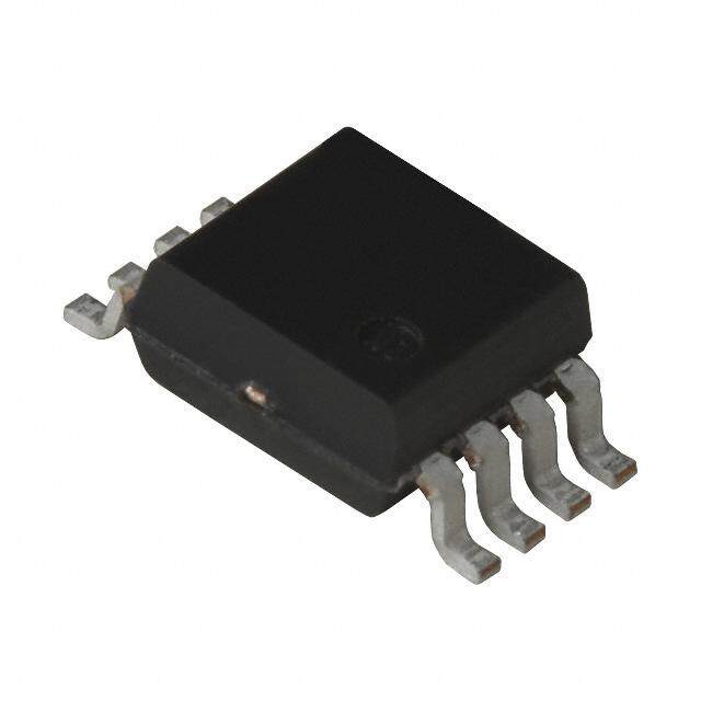
| 产品图片 |
|
| rohs | 符合RoHS无铅 / 符合限制有害物质指令(RoHS)规范要求 |
| 产品系列 | 驱动器IC,显示驱动器和控制器,NXP Semiconductors UBA2021P/N2,112- |
| 数据手册 | |
| 产品型号 | UBA2021P/N2,112 |
| PCN封装 | |
| 产品 | CFL, Fluorescent TL Drivers |
| 产品培训模块 | http://www.digikey.cn/PTM/IndividualPTM.page?site=cn&lang=zhs&ptm=25733 |
| 产品目录页面 | |
| 产品种类 | 显示驱动器和控制器 |
| 供应商器件封装 | 14-DIP |
| 其它名称 | 568-4928-5 |
| 制造商卷带宽度 | - |
| 制造商卷带材料 | - |
| 制造商卷带直径 | - |
| 包装 | 管件 |
| 商标 | NXP Semiconductors |
| 图号 | 568; SOT27-1; BP, D, N, N2, P ; 14 |
| 安装类型 | 通孔 |
| 安装风格 | Through Hole |
| 封装 | Tube |
| 封装/外壳 | 14-DIP(0.300",7.62mm) |
| 封装/箱体 | PDIP-14 |
| 工作温度 | -40°C ~ 150°C |
| 工厂包装数量 | 1120 |
| 最大功率耗散 | 500 mW |
| 最大工作温度 | + 150 C |
| 最大输出电流 | 35 mA |
| 最小工作温度 | - 40 C |
| 标准包装 | 28 |
| 电压-电源 | 10.15 V ~ 11.95 V |
| 电流-灌/拉输出 | - |
| 电流-电源 | 1mA |
| 电源电压 | 630 V |
| 电源电流 | 1 mA |
| 类型 | CFL/TL 控制器 |
| 调光 | 无 |
| 零件号别名 | UBA2021PN |
| 频率 | 41.21kHz ~ 44.59kHz |





- 商务部:美国ITC正式对集成电路等产品启动337调查
- 曝三星4nm工艺存在良率问题 高通将骁龙8 Gen1或转产台积电
- 太阳诱电将投资9.5亿元在常州建新厂生产MLCC 预计2023年完工
- 英特尔发布欧洲新工厂建设计划 深化IDM 2.0 战略
- 台积电先进制程称霸业界 有大客户加持明年业绩稳了
- 达到5530亿美元!SIA预计今年全球半导体销售额将创下新高
- 英特尔拟将自动驾驶子公司Mobileye上市 估值或超500亿美元
- 三星加码芯片和SET,合并消费电子和移动部门,撤换高东真等 CEO
- 三星电子宣布重大人事变动 还合并消费电子和移动部门
- 海关总署:前11个月进口集成电路产品价值2.52万亿元 增长14.8%


PDF Datasheet 数据手册内容提取
UBA2021 630 V driver IC for CFL and TL lamps Rev. 04 — 25 July 2008 Product data sheet 1. General description The UBA2021 is a high voltage IC intended to drive and control Compact Fluorescent Lamps (CFL) or fluorescent TL lamps. It contains a driver circuit for an external half-bridge, an oscillator and a control circuit for starting up, preheating, ignition, lamp burning and protection. 2. Features n Adjustable preheat and ignition time. n Adjustable preheat current. n Adjustable lamp power. n Lamp power independent from mains voltage variations. n Overpower protection. n Lamp temperature stress protection at higher mains voltages. n Capacitive mode protection. n Protection against a drive voltage that is too low for the power MOSFETs. 3. Quick reference data Table 1. Quick reference data Symbol Parameter Conditions Min Typ Max Unit High voltage supply V high side supply voltage I <15m A; t <0.5s - - 630 V FS FS Start-up state V oscillator start voltage - 11.95 - V VS(start) V oscillator stop voltage - 10.15 - V VS(stop) I standby current V = 11 V - 200 - m A VS(standby) VS Preheat mode f start frequency - 108 - kHz start t preheat time C = 100 nF - 666 - ms ph CP V control voltage at pin RS - - 600 - mV RS(ctrl) Frequency sweep to ignition f bottom frequency - 42.9 - kHz B t ignition time - 625 - ms ign Normal operation f bottom frequency - 42.9 - kHz B t non-overlap time - 1.4 - m s no
UBA2021 NXP Semiconductors 630 V driver IC for CFL and TL lamps Table 1. Quick reference data Symbol Parameter Conditions Min Typ Max Unit I total supply current f = 43 kHz - 1 - mA tot B R , high and low side on - 126 - W G1(on) R resistance G2(on) R , high and low side off - 75 - W G1(off) R resistance G2(off) Feed-forward f feed-forward frequency I = 0.75 mA - 63.6 - kHz ff RHV I = 1.0 mA - 84.5 - kHz RHV I operating range of input 0 - 1000 m A i(RHV) current at pin RHV 4. Ordering information Table 2. Ordering information Type number Package Name Description Version UBA2021T SO14 plastic small outline package; 14 leads; body width 3.9 mm SOT108-1 UBA2021P DIP14 plastic dual in-line package; 14 leads (300 mil) SOT27-1 5. Block diagram VS RHV RREF CF CI 5 13 10 12 14 bootstrap charging circuit SB SUPPLY 1 FS n.c. 4 OSCILLATOR LEVEL HIGH SIDE 2 G1 SHIFTER DRIVER 3 BAND GAP S1 REFERENCE 8 NON CP TIMING OVERLAP LOW SIDE 6 G2 DRIVER 9 RS 7 RS MONITOR CONTROL UBA2021 PGND 11 mgs988 SGND Fig 1. Block diagram UBA2021_4 © NXP B.V. 2008. All rights reserved. Product data sheet Rev. 04 — 25 July 2008 2 of 16
UBA2021 NXP Semiconductors 630 V driver IC for CFL and TL lamps 6. Pinning information 6.1 Pinning FS 1 14 CI FS 1 14 CI G1 2 13 RHV G1 2 13 RHV S1 3 12 CF S1 3 12 CF n.c. 4 UBA2021T 11 SGND n.c. 4 UBA2021P 11 SGND VS 5 10 RREF VS 5 10 RREF G2 6 9 RS G2 6 9 RS PGND 7 8 CP PGND 7 8 CP 001aai566 001aai567 Fig 2. Pin configuration (SO14) Fig 3. Pin configuration (DIP14) 6.2 Pin description Table 3. Pin description Symbol Pin Description FS 1 high side floating supply voltage G1 2 gate high transistor (T1) S1 3 source high transistor (T1) n.c. 4 high-voltage spacer, not to be connected VS 5 low voltage supply G2 6 gate low transistor (T2) PGND 7 power ground CP 8 timing/averaging capacitor RS 9 current monitoring input RREF 10 reference resistor SGND 11 signal ground CF 12 oscillator capacitor RHV 13 start-up resistor/feed-forward resistor CI 14 integrating capacitor 7. Functional description 7.1 Introduction The UBA2021 is an integrated circuit for electronically ballasted compact fluorescent lamps and their derivatives operating with mains voltages up to 240 V (RMS). It provides all the necessary functions for preheat, ignition and on-state operation of the lamp. In addition to the control function, the IC provides level shift and drive functions for the two discrete power MOSFETs, T1 and T2 (seeFigure7). UBA2021_4 © NXP B.V. 2008. All rights reserved. Product data sheet Rev. 04 — 25 July 2008 3 of 16
UBA2021 NXP Semiconductors 630 V driver IC for CFL and TL lamps 7.2 Initial start-up Initial start-up is achieved by charging capacitor CS9 with the current applied to the RHV-pin.Atstart-up,MOSFETT2conductsandT1doesnotconduct.ThisensuresC boot becomes charged. This start-up state is reached for a supply voltage of V . This is VS(reset) the voltage level on the VS-pin at which the circuit will be reset to its initial state and maintained until the low voltage supply (V ) reaches a value of V . The circuit is VS VS(start) reset to the start-up state. 7.3 Oscillation When the low voltage supply (V ) has reached the value of V the circuit starts VS VS(start) oscillating in the preheat state. The internal oscillator is a current-controlled circuit which generates a sawtooth waveform. The frequency of the sawtooth is determined by the capacitor C and the current out of the CF-pin, mainly set by R . The sawtooth CF RREF frequency is twice the frequency of the signal across the load. The IC brings MOSFETs T1 and T2 alternately into conduction with a duty factor of approximately 50 %.Figure4 represents the timing of the IC. The circuit block 'non-overlap' generates a non-overlap timet thatensuresconductionperiodsofexclusivelyT1orT2.Timet isdependenton no no the reference current I . RREF start-up VCF 0 internal clock 0 V(G1-S1) 0 V(G2) tno tno 0 time mgs991 Fig 4. Oscillator timing 7.4 Operation in the preheat mode The circuit starts oscillating at approximately 2.5· f (108 kHz). The frequency gradually B decreasesuntiladefinedvalueofcurrentI isreached(seeFigure5).Theslopeofthe shunt decreaseinfrequencyisdeterminedbycapacitorC .Thefrequencyduringpreheatingis CI approximately 90 kHz. This frequency is well above the resonant frequency of the load, which means that the lamp is off, the load only consists of L2, C5 and the electrode resistance.ThepreheattimeisdeterminedbycapacitorC .Thecircuitcanbelockedin CP the preheat state by connecting the CP-pin to ground. During preheating, the circuit monitors the load current by measuring the voltage drop over external resistor R at shunt the end of conduction of T2 with decision level V . The frequency is decreased as long as RS(ctrl) V >V . The frequency is increased for V < V . RS RS(ctrl) RS RS(ctrl) UBA2021_4 © NXP B.V. 2008. All rights reserved. Product data sheet Rev. 04 — 25 July 2008 4 of 16
UBA2021 NXP Semiconductors 630 V driver IC for CFL and TL lamps fstart fB ignition preheat state burn state state time mgs992 Fig 5. Operation in the preheat mode 7.5 Ignition state The RS monitoring function changes from V regulation to capacitive mode RS(ctrl) protection at the end of the preheat time. Normally this results in a further frequency decrease down to the bottom frequency f (approximately 43 kHz). The rate of change of B frequencyintheignitionstateislessthanthatinthepreheatmode.Duringthedownward frequency sweep the circuit sweeps through the resonant frequency of the load. A high voltage then appears across the lamp. This voltage normally ignites the lamp. 7.6 Failure to ignite Excessive current levels may occur if the lamp fails to ignite. The IC does not limit these currents in any way. 7.7 Transition to the burn state Assumingthatthelamphasignitedduringthedownwardfrequencysweep,thefrequency normally decreases to the bottom frequency. The IC can transit to the burn state in two ways: 1. In the event that the bottom frequency is not reached, transition is made after reaching the ignition time t . ign 2. As soon as the bottom frequency is reached. The bottom frequency is determined by R and C . RREF CF 7.8 Feed-forward frequency During burn state a feed-forward mechanism ensures that the lamp power will not increase above the maximum allowed value due to an increased mains voltage. In the feed-forward range the UBA2021 driver IC can be configured in such a way that the application is optimized for close to constant lamp power. Above a defined voltage level the oscillation frequency also depends on the supply voltage of the half-bridge (see Figure6). The current for the current controlled oscillator is derived from the current throughR inthefeed-forwardrange.Thefeed-forwardfrequencyisproportionaltothe RHV average value of the current through R within the operating range of I , given the RHV i(RHV) lowerlimitsetbyf .Forcurrentsbeyondtheoperatingrange(i.e.between1.0mAand1.6 B mA) the feed-forward frequency is clamped. In order to prevent feed-forward of ripple on UBA2021_4 © NXP B.V. 2008. All rights reserved. Product data sheet Rev. 04 — 25 July 2008 5 of 16
UBA2021 NXP Semiconductors 630 V driver IC for CFL and TL lamps V , the ripple is filtered out. The capacitor connected to the CP-pin is used for this in purpose.Thispinisalsousedinthepreheatstateandtheignitionstatefortiming(t and ph t ). ign f (kHz) feed-forward range bottom frequency IRHV (mA) mgs993 Fig 6. Feed-forward frequency 7.9 Capacitive mode protection When the preheat mode is completed, the IC will protect the power circuit against losing the zero voltage switching condition and getting too close to the capacitive mode of operation.ThisisdetectedbymonitoringvoltageV attheRS-pin.Ifthevoltageisbelow RS V at the time of turn-on of T2, the capacitive mode operation is assumed. RS(cap) Consequently the frequency increases as long as the capacitive mode is detected. The frequency decreases down to the feed-forward frequency if no capacitive mode is detected. Frequency modulation is achieved via the CI-pin. 7.10 IC supply Initially, the IC is supplied from V by the current through R . This current charges the in RHV supply capacitor CS9 via an internal diode. As soon as V exceeds V , the circuit VS VS(start) starts oscillating. After the preheat phase is finished, the pin is connected to an internal resistorR ,priortothistheRHV-pinisinternallyconnectedtotheVS-pin.Thevoltage i(RHV) level at the RHV-pin thus drops from V + V to I · R . The capacitor CS9 at VS diode RHV i(RHV) the VS-pin will now be charged via the snubber capacitor CS7. Excess charge is drained by an internal clamp that turns on at voltage V . VS(clamp) 7.11 Minimum gate-source voltage of T1 and T2 The high side driver is supplied via capacitor C . Capacitor C is charged via the boot boot bootstrap switch during the on periods of T2. The IC stops oscillating at a voltage level V . Given a maximum charge consumption on the load at the G1-pin of 1 nC/V, this VS(stop) safeguards the minimum drive voltages V for the high side driver, seeTable1. (G1-S1) Table 4. Minimum gate-source voltages FREQUENCY VOLTAGE < 75 kHz 8 V (min) 75 kHz to 85 kHz 7 V (min) ‡ 85 kHz 6 V (min) The drive voltage at G2 will exceed the drive voltage of the high side driver. UBA2021_4 © NXP B.V. 2008. All rights reserved. Product data sheet Rev. 04 — 25 July 2008 6 of 16
UBA2021 NXP Semiconductors 630 V driver IC for CFL and TL lamps 7.12 Frequency and change in frequency At any point in time during oscillation, the circuit will operate between f and f . Any B start change in frequency will be gradual, no steps in frequency will occur. Changes in frequency caused by a change in voltage at the CI-pin show a rather constantD f/D t over theentirefrequencyrange.Thefollowingratesarerealized(atafrequencyof85kHzand with a 100 nF capacitor connected to the PCI-pin): • For any increase in frequency:D f/D t is between 15 kHz/ms and 37.5 kHz/ms. • During preheat and normal operation:D f/D t for a decrease in frequency is between - 6kHz/ms and- 15 kHz/ms. • During the ignition phase:D f/D t for a decrease in frequency is between - 150Hz/msand- 375 Hz/ms. 7.13 Ground pins The PGND-pin is the ground reference of the IC with respect to the application. As an exceptiontheSGND-pinprovidesalocalgroundreferenceforthecomponentsconnected to the CP-pin, CI-pin, RREF-pin and thee CF-pin. For this purpose the PGND-pin and SGND-pin are short circuited internally. External connection of the PGND-pin and the SGND-pin is not preferred. The sum of currents flowing out of the CP-pin, CI-pin, RREF-pin, CF-pin and the SGND-pin must remain zero at all time. 7.14 Charge coupling Duetoparasiticcapacitivecouplingtothehighvoltagecircuitry,allpinsareburdenedwith a repetitive charge injection. Given the typical application inFigure7, the RREF-pin and the CF-pin are sensitive to this charge injection. For the rating Q a safe functional couple operation of the IC is guaranteed, independent of the current level. Charge coupling at current levels below 50 mA will not interfere with the accuracy of the V and V RS(cap) RS(ctrl) levels. Charge coupling at current levels below 20 mA will not interfere with the accuracy of any parameter. 8. Limiting values Table 5. Limiting values In accordance with the Absolute Maximum Rating System (IEC 60134). All voltages referenced to ground. Symbol Parameter Conditions Min Max Unit V high side floating supply operating - 570 V FS voltage t£ 0.5 s - 630 V I clamp current - 35 mA VS(clamp) V input voltage pin RS - 2.5 +2.5 V RS transient of 50 ns - 15 +2.5 V SR slew rate at pins S1, G1 - 4 +4 V/ns and FS (with respect to ground) P power dissipation - 500 mW T ambient temperature - 40 +150 (cid:176) C amb T junction temperature - 40 +150 (cid:176) C j UBA2021_4 © NXP B.V. 2008. All rights reserved. Product data sheet Rev. 04 — 25 July 2008 7 of 16
UBA2021 NXP Semiconductors 630 V driver IC for CFL and TL lamps Table 5. Limiting values …continued In accordance with the Absolute Maximum Rating System (IEC 60134). All voltages referenced to ground. Symbol Parameter Conditions Min Max Unit T storage temperature - 55 +150 (cid:176) C stg Q charge coupling at pins operating - 8 +8 pC couple RREF and CF V electrostatic handling human body [1] - 2000 V es voltage model machine model [2] - 250 V [1] HBM: 2000 V, except pins FS, G1, S1 and VS which are 1000 V maximum and G2 which is 800 V maximum. [2] MM: 250 V except for the G1-pin which is 100 V. 9. Thermal characteristics Table 6. Thermal characteristics Symbol Parameter Conditions Typ Unit R thermal resistance from junction in free air th(j-a) to ambient S014 100 K/W DIP14 60 K/W R thermal resistance from junction in free air th(j-pin) to PCB S014 50 K/W DIP14 30 K/W 10. Characteristics Table 7. Characteristics V = 11 V; V - V = 11 V; T = 25(cid:176) C; all voltages referenced to ground; unless otherwise specified. SeeFigure8. VS FS S1 amb Symbol Parameter Conditions Min Typ Max Unit High voltage supply I leakage current on high V ,V andV =630V - - 15 m A L FS G1 S1 voltage pins Start-up state V reset voltage T1 off; T2 on 4 5.5 6.5 V VS(reset) V oscillator start voltage 11.35 11.95 12.55 V VS(start) V oscillator stop voltage 9.55 10.15 10,75 V VS(stop) V supply voltage hysteresis 1.5 1.8 2 V VS(hys) I standbysupplycurrentatpin V = 11 V [1] 150 200 250 m A VS(standby) VS VS D V voltage difference between I = 1.0 mA 0.7 0.8 1 V (RHV-VS) RHV pins RHV and VS V clamp margin V to [2] 0.2 0.3 0.4 V VS(clamp-start) VS(clamp) V VS(start) UBA2021_4 © NXP B.V. 2008. All rights reserved. Product data sheet Rev. 04 — 25 July 2008 8 of 16
UBA2021 NXP Semiconductors 630 V driver IC for CFL and TL lamps Table 7. Characteristics …continued V = 11 V; V - V = 11 V; T = 25(cid:176) C; all voltages referenced to ground; unless otherwise specified. SeeFigure8. VS FS S1 amb Symbol Parameter Conditions Min Typ Max Unit I clamp current V < 17 V - 14 35 mA VS(clamp) VS Preheat mode f starting frequency V = 0 V 98 108 118 kHz start CI t conducting time T1 and T2 f = 108 kHz - 3.2 - m s g start I charge current at pin CI V = 1.5 V; V =- 0.3 V 38 44 50 m A CI(charge) CI RS I discharge current at pin CI V = 1.5 V; V =- 0.9 V 79 93 107 m A CI(discharge) CI RS t preheat time 599 666 733 ms ph I charge current at pin CP V = 1 V - 6 - m A CP(charge) CP I discharge current at pin CP V = 1 V - 5.95 - m A CP(discharge) CP D V peak voltage difference at when timing - 2.5 - V CP(pk) pin CP V control voltage at pin RS [3] - 636 - 600 - 564 mV RS(ctrl) Frequency sweep to ignition I charge current at pin CI V = 1.5 V; f» 85 kHz 0.8 1 1.2 m A CI(charge) CI f bottom frequency V at clamp level - 42.9 - kHz B CI t ignition time - 625 - m s ign Normal operation f bottom frequency 41.21 42.9 44.59 kHz B tg conducting time T1 and T2 fB= 43 kHz - 10.2 - m s t non-overlap conductance 1.05 1.4 1.75 m s no time I total supply current f = 43 kHz [4] 0.85 1 1.1 mA tot B V capacitive mode control [5] 0 20 40 mV RS(cap) voltage V reference voltage [6] 2.425 2.5 2.575 V RREF V on voltage at pin G1 (cid:239) I (cid:239) = 1 mA 10.5 - - V G1(on) G1 V off voltage at pin G1 (cid:239) I (cid:239) = 1 mA - - 0.3 V G1(off) G1 V on voltage at pin G2 (cid:239) I (cid:239) = 1 mA 10.5 - - V G2(on) G2 V off voltage at pin G2 (cid:239) I (cid:239) = 1 mA - - 0.3 V G2(off) G2 R high side driver on V = 3 V [7] 100 126 152 W G1(on) (G1 - S1) resistance R high side driver off V = 3 V [7] 60 75 90 W G1(off) (G1 - S1) resistance R low side driver on resistance V = 3 V [7] 100 126 152 W G2(on) G2 R low side driver off resistance V = 3 V [7] 60 75 90 W G2(off) G2 Vdrop voltage drop at bootstrap IFS= 5 mA 0.6 1 1.4 V switch Feed-forward R input resistance at pin RHV [8] 1.54 2.2 2.86 kW i(RHV) I operating range of input 0 - 1000 m A i(RHV) current at pin RHV UBA2021_4 © NXP B.V. 2008. All rights reserved. Product data sheet Rev. 04 — 25 July 2008 9 of 16
UBA2021 NXP Semiconductors 630 V driver IC for CFL and TL lamps Table 7. Characteristics …continued V = 11 V; V - V = 11 V; T = 25(cid:176) C; all voltages referenced to ground; unless otherwise specified. SeeFigure8. VS FS S1 amb Symbol Parameter Conditions Min Typ Max Unit f feed-forward frequency I = 0.75 mA 60.4 63.6 66.15 kHz ff RHV I = 1 mA 80.3 84.5 88.2 kHz RHV SYM symmetry I = 1 mA [9] 0.9 1 1.1 ff RHV RR ripple rejection f = 100 Hz - 6 - dB Vin RCP(sw) CP switch series resistance ICP= 100m A 0.75 1.5 2.25 kW RAV averaging resistor ICP= 10m A 22.4 32 41.6 kW [1] Thestart-upsupplycurrentisspecifiedinatemperature(T )rangeof0(cid:176) Cto125(cid:176) C.ForT <0(cid:176) CandT >125(cid:176) Cthestart-upsupply vj vj vj current is < 350m A. [2] Theclampmarginisdefinedasthevoltagedifferencebetweenturn-onoftheclampandstartofoscillation.Theclampisintheoff-state at start of oscillation. [3] Data sampling of V is performed at the end of conduction of T2. RS(ctrl) [4] Thetotalsupplycurrentisspecifiedinatemperature(T )rangeof- 20(cid:176) Cto+125(cid:176) C.ForT <- 20(cid:176) CandT >125(cid:176) Cthetotalsupply vj vj vj current is < 1.5 mA. [5] Data sampling of V is performed at the start of conduction of T2. RS(cap) [6] Within the allowed range of R , defined as 30 kW +10 %. RREF [7] Typical values for the on and off resistances at T = 87.5(cid:176) C are: R and R = 164W , R and R = 100W . vj G2(on) G1(on) G2(off) G1(off) [8] The input current at RHV pin may increase to 1600m A during voltage transient at V . Only for currents I beyond approximately in RHV 550m A is the oscillator frequency proportional to I . RHV [9] The symmetry SYM is calculated from the quotient SYM = T1 / T2 , with T1 the time between turn-off of G2 and turn-off of G1, ff ff tot tot tot and T2 the time between turn-off of G1 and turn-off of G2. tot 11. Design information 11.1 Design equations • Bottom frequency: 1 f = ------------------------------------------------------------------------------------------------------------------------ (1) B 2· {[(C +C )· (X1· R –R )]+t } CF par RREF int • Feed-forward frequency: 1 f = -------------------------------------------------------------------------------------------------------------------------- (2) ff 2· (cid:238)(cid:237)(cid:236) (CCF+Cpar)· Ł(cid:230) -X----2--I--i·--(--R-V--H---R-V--R-)--E---F--–Rinł(cid:246)t +t (cid:254)(cid:253)(cid:252) • Where: – X1 = 3.68. – X2 = 22.28. – t = 0.4m s. – R = 3 kW . int – C = 4.7 pF par • Operating frequency is the maximum of f , f or f . B ff cm UBA2021_4 © NXP B.V. 2008. All rights reserved. Product data sheet Rev. 04 — 25 July 2008 10 of 16
UBA2021 NXP Semiconductors 630 V driver IC for CFL and TL lamps • Where: • f = bottom frequency. B • f = feed-forward frequency. ff • f = frequency due to capacitive mode detection. cm C R • Preheat time:t = --------C---P-----· -----R---R---E---F-- ph 150nF 30KW 15 • Ignition time: t = ------· t ign 16 ph R • Non-overlap time:t = 1.4m s· -----R---R---E---F-- no 30kW 12. Application information L1 Vin RRHV 490 kW RHV CCI T1 G1 13 CI DS1 DS2 C3 2 14 lamp 100 nF CCP S1 CP R1 3 8 100 nF mains L2 100 nF CCF supply C2 CS7 FS 1 UBA2021 12 CF C5 Cboot 100 pF RRREF T2 G2 RREF 6 10 30 kW DS7 VS SGND 5 7 9 11 DS3 DS4 C4 CS4 DS6 CS9 PGND RS Rshunt mgs994 Fig 7. Application diagram UBA2021_4 © NXP B.V. 2008. All rights reserved. Product data sheet Rev. 04 — 25 July 2008 11 of 16
UBA2021 NXP Semiconductors 630 V driver IC for CFL and TL lamps 13. Package outline DIP14: plastic dual in-line package; 14 leads (300 mil) SOT27-1 D ME e n a pl g n eati A2 A s L A1 c Z e w M b1 (e ) 1 b 14 8 MH pin 1 index E 1 7 0 5 10 mm scale DIMENSIONS (inch dimensions are derived from the original mm dimensions) UNIT mAax. mAi n1 . mAa 2x . b b1 c D(1) E(1) e e1 L ME MH w mZax(1.) 1.73 0.53 0.36 19.50 6.48 3.60 8.25 10.0 mm 4.2 0.51 3.2 2.54 7.62 0.254 2.2 1.13 0.38 0.23 18.55 6.20 3.05 7.80 8.3 0.068 0.021 0.014 0.77 0.26 0.14 0.32 0.39 inches 0.17 0.02 0.13 0.1 0.3 0.01 0.087 0.044 0.015 0.009 0.73 0.24 0.12 0.31 0.33 Note 1. Plastic or metal protrusions of 0.25 mm (0.01 inch) maximum per side are not included. OUTLINE REFERENCES EUROPEAN ISSUE DATE VERSION IEC JEDEC JEITA PROJECTION 99-12-27 SOT27-1 050G04 MO-001 SC-501-14 03-02-13 Fig 8. DIP14: plastic dual in-line package; UBA2021_4 © NXP B.V. 2008. All rights reserved. Product data sheet Rev. 04 — 25 July 2008 12 of 16
UBA2021 NXP Semiconductors 630 V driver IC for CFL and TL lamps SO14: plastic small outline package; 14 leads; body width 3.9 mm SOT108-1 D E A X c y HE v M A Z 14 8 Q A2 A1 (A 3 ) A pin 1 index q Lp 1 7 L e w M detail X bp 0 2.5 5 mm scale DIMENSIONS (inch dimensions are derived from the original mm dimensions) UNIT mAax. A1 A2 A3 bp c D(1) E(1) e HE L Lp Q v w y Z(1) q 0.25 1.45 0.49 0.25 8.75 4.0 6.2 1.0 0.7 0.7 mm 1.75 0.25 1.27 1.05 0.25 0.25 0.1 0.10 1.25 0.36 0.19 8.55 3.8 5.8 0.4 0.6 0.3 8o 0.010 0.057 0.019 0.0100 0.35 0.16 0.244 0.039 0.028 0.028 0o inches 0.069 0.01 0.05 0.041 0.01 0.01 0.004 0.004 0.049 0.014 0.0075 0.34 0.15 0.228 0.016 0.024 0.012 Note 1. Plastic or metal protrusions of 0.15 mm (0.006 inch) maximum per side are not included. OUTLINE REFERENCES EUROPEAN ISSUE DATE VERSION IEC JEDEC JEITA PROJECTION 99-12-27 SOT108-1 076E06 MS-012 03-02-19 Fig 9. SO14 plastic small outline package UBA2021_4 © NXP B.V. 2008. All rights reserved. Product data sheet Rev. 04 — 25 July 2008 13 of 16
UBA2021 NXP Semiconductors 630 V driver IC for CFL and TL lamps 14. Revision history Table 8. Revision history Document ID Release date Data sheet status Change notice Supersedes UBA2021_4 20080725 Product data sheet - UBA2021_3 Modifications: • The format of this data sheet has been redesigned to comply with the new identity guidelines of NXP Semiconductors. • Legal texts have been adapted to the new company name where appropriate. UBA2021_3 20080802 Product data sheet - UBA2021_2 UBA2021_2 20010130 Product data sheet - UBA2021_1 UBA2021_1 20000724 Product data sheet - - UBA2021_4 © NXP B.V. 2008. All rights reserved. Product data sheet Rev. 04 — 25 July 2008 14 of 16
UBA2021 NXP Semiconductors 630 V driver IC for CFL and TL lamps 15. Legal information 15.1 Data sheet status Document status[1][2] Product status[3] Definition Objective [short] data sheet Development This document contains data from the objective specification for product development. Preliminary [short] data sheet Qualification This document contains data from the preliminary specification. Product [short] data sheet Production This document contains the product specification. [1] Please consult the most recently issued document before initiating or completing a design. [2] The term ‘short data sheet’ is explained in section “Definitions”. [3] Theproductstatusofdevice(s)describedinthisdocumentmayhavechangedsincethisdocumentwaspublishedandmaydifferincaseofmultipledevices.Thelatestproductstatus information is available on the Internet at URLhttp://www.nxp.com. 15.2 Definitions damage. NXP Semiconductors accepts no liability for inclusion and/or use of NXP Semiconductors products in such equipment or applications and therefore such inclusion and/or use is at the customer’s own risk. Draft —The document is a draft version only. The content is still under internal review and subject to formal approval, which may result in Applications —Applications that are described herein for any of these modifications or additions. NXP Semiconductors does not give any products are for illustrative purposes only. NXP Semiconductors makes no representations or warranties as to the accuracy or completeness of representation or warranty that such applications will be suitable for the informationincludedhereinandshallhavenoliabilityfortheconsequencesof specified use without further testing or modification. use of such information. Quick reference data —The Quick reference data is an extract of the Short data sheet —A short data sheet is an extract from a full data sheet product data given in the Limiting values and Characteristics sections of this withthesameproducttypenumber(s)andtitle.Ashortdatasheetisintended document, and as such is not complete, exhaustive or legally binding. forquickreferenceonlyandshouldnotbereliedupontocontaindetailedand Limiting values —Stress above one or more limiting values (as defined in full information. For detailed and full information see the relevant full data theAbsoluteMaximumRatingsSystemofIEC60134)maycausepermanent sheet, which is available on request via the local NXP Semiconductors sales damagetothedevice.Limitingvaluesarestressratingsonlyandoperationof office. In case of any inconsistency or conflict with the short data sheet, the the device at these or any other conditions above those given in the full data sheet shall prevail. Characteristics sections of this document is not implied. Exposure to limiting values for extended periods may affect device reliability. 15.3 Disclaimers Terms and conditions of sale —NXP Semiconductors products are sold subjecttothegeneraltermsandconditionsofcommercialsale,aspublished athttp://www.nxp.com/profile/terms, including those pertaining to warranty, General —Information in this document is believed to be accurate and intellectual property rights infringement and limitation of liability, unless reliable.However,NXPSemiconductorsdoesnotgiveanyrepresentationsor explicitly otherwise agreed to in writing by NXP Semiconductors. In case of warranties,expressedorimplied,astotheaccuracyorcompletenessofsuch any inconsistency or conflict between information in this document and such information and shall have no liability for the consequences of use of such terms and conditions, the latter will prevail. information. No offer to sell or license —Nothing in this document may be interpreted Right to make changes —NXPSemiconductorsreservestherighttomake or construed as an offer to sell products that is open for acceptance or the changes to information published in this document, including without grant,conveyanceorimplicationofanylicenseunderanycopyrights,patents limitation specifications and product descriptions, at any time and without or other industrial or intellectual property rights. notice.Thisdocumentsupersedesandreplacesallinformationsuppliedprior to the publication hereof. Suitability for use —NXP Semiconductors products are not designed, 15.4 Trademarks authorized or warranted to be suitable for use in medical, military, aircraft, space or life support equipment, nor in applications where failure or Notice:Allreferencedbrands,productnames,servicenamesandtrademarks malfunction of an NXP Semiconductors product can reasonably be expected are the property of their respective owners. to result in personal injury, death or severe property or environmental 16. Contact information For more information, please visit:http://www.nxp.com For sales office addresses, please send an email to:salesaddresses@nxp.com UBA2021_4 © NXP B.V. 2008. All rights reserved. Product data sheet Rev. 04 — 25 July 2008 15 of 16
UBA2021 NXP Semiconductors 630 V driver IC for CFL and TL lamps 17. Contents 1 General description. . . . . . . . . . . . . . . . . . . . . . 1 2 Features . . . . . . . . . . . . . . . . . . . . . . . . . . . . . . . 1 3 Quick reference data. . . . . . . . . . . . . . . . . . . . . 1 4 Ordering information. . . . . . . . . . . . . . . . . . . . . 2 5 Block diagram . . . . . . . . . . . . . . . . . . . . . . . . . . 2 6 Pinning information. . . . . . . . . . . . . . . . . . . . . . 3 6.1 Pinning . . . . . . . . . . . . . . . . . . . . . . . . . . . . . . . 3 6.2 Pin description . . . . . . . . . . . . . . . . . . . . . . . . . 3 7 Functional description . . . . . . . . . . . . . . . . . . . 3 7.1 Introduction. . . . . . . . . . . . . . . . . . . . . . . . . . . . 3 7.2 Initial start-up . . . . . . . . . . . . . . . . . . . . . . . . . . 4 7.3 Oscillation. . . . . . . . . . . . . . . . . . . . . . . . . . . . . 4 7.4 Operation in the preheat mode. . . . . . . . . . . . . 4 7.5 Ignition state. . . . . . . . . . . . . . . . . . . . . . . . . . . 5 7.6 Failure to ignite. . . . . . . . . . . . . . . . . . . . . . . . . 5 7.7 Transition to the burn state. . . . . . . . . . . . . . . . 5 7.8 Feed-forward frequency . . . . . . . . . . . . . . . . . . 5 7.9 Capacitive mode protection . . . . . . . . . . . . . . . 6 7.10 IC supply. . . . . . . . . . . . . . . . . . . . . . . . . . . . . . 6 7.11 Minimum gate-source voltage of T1 and T2. . . 6 7.12 Frequency and change in frequency. . . . . . . . . 7 7.13 Ground pins . . . . . . . . . . . . . . . . . . . . . . . . . . . 7 7.14 Charge coupling . . . . . . . . . . . . . . . . . . . . . . . . 7 8 Limiting values. . . . . . . . . . . . . . . . . . . . . . . . . . 7 9 Thermal characteristics. . . . . . . . . . . . . . . . . . . 8 10 Characteristics. . . . . . . . . . . . . . . . . . . . . . . . . . 8 11 Design information . . . . . . . . . . . . . . . . . . . . . 10 11.1 Design equations . . . . . . . . . . . . . . . . . . . . . . 10 12 Application information. . . . . . . . . . . . . . . . . . 11 13 Package outline . . . . . . . . . . . . . . . . . . . . . . . . 12 14 Revision history. . . . . . . . . . . . . . . . . . . . . . . . 14 15 Legal information. . . . . . . . . . . . . . . . . . . . . . . 15 15.1 Data sheet status . . . . . . . . . . . . . . . . . . . . . . 15 15.2 Definitions. . . . . . . . . . . . . . . . . . . . . . . . . . . . 15 15.3 Disclaimers. . . . . . . . . . . . . . . . . . . . . . . . . . . 15 15.4 Trademarks. . . . . . . . . . . . . . . . . . . . . . . . . . . 15 16 Contact information. . . . . . . . . . . . . . . . . . . . . 15 17 Contents. . . . . . . . . . . . . . . . . . . . . . . . . . . . . . 16 Pleasebeawarethatimportantnoticesconcerningthisdocumentandtheproduct(s) described herein, have been included in section ‘Legal information’. © NXP B.V. 2008. All rights reserved. For more information, please visit: http://www.nxp.com For sales office addresses, please send an email to: salesaddresses@nxp.com Date of release: 25 July 2008 Document identifier: UBA2021_4

 Datasheet下载


