ICGOO在线商城 > 集成电路(IC) > PMIC - 稳压器 - 线性 > UA79M05CKVURG3

 Datasheet下载
- 型号: UA79M05CKVURG3
- 制造商: Texas Instruments
- 库位|库存: xxxx|xxxx
- 要求:
| 数量阶梯 | 香港交货 | 国内含税 |
| +xxxx | $xxxx | ¥xxxx |
查看当月历史价格
查看今年历史价格
UA79M05CKVURG3产品简介:
ICGOO电子元器件商城为您提供UA79M05CKVURG3由Texas Instruments设计生产,在icgoo商城现货销售,并且可以通过原厂、代理商等渠道进行代购。 UA79M05CKVURG3价格参考。Texas InstrumentsUA79M05CKVURG3封装/规格:PMIC - 稳压器 - 线性, Linear Voltage Regulator IC Negative Fixed 1 Output -5V 500mA TO-252-3。您可以下载UA79M05CKVURG3参考资料、Datasheet数据手册功能说明书,资料中有UA79M05CKVURG3 详细功能的应用电路图电压和使用方法及教程。
Texas Instruments 的 UA79M05CKVURG3 是一款线性稳压器(LM79M系列),属于负电压稳压器,输出电压为-5V,常用于需要稳定负电压供电的电子电路中。

该器件主要应用于以下场景:

1. 模拟电路供电:如运算放大器、比较器等需要负电源的模拟系统中,提供稳定可靠的负电压源。

2. 通信设备:在一些通信模块或接口电路中,如RS-232电平转换器,需要负电压驱动,UA79M05可为其提供稳定电源。

3. 工业控制系统:用于PLC、传感器模块、测量仪器等工业设备中的负电压供电需求。

4. 嵌入式系统与开发板:某些微控制器或特定功能芯片需要双电源供电(+5V和-5V),此稳压器可用于构建紧凑的负电压电源部分。

5. 消费电子产品:如音频设备、便携式仪器等,适用于对噪声敏感且需要低纹波负电压的场合。

该器件采用小型封装(如SOT-223),具备过热和短路保护功能,适合空间有限但要求稳定性的应用环境。由于是线性稳压器,适用于输入输出压差较小、功耗不高的场景。
| 参数 | 数值 |
| 产品目录 | 集成电路 (IC)半导体 |
| 描述 | IC REG LDO -5V 0.5A TO252-3线性稳压器 5V 500mA Fixed Neg Voltage Regulator |
| 产品分类 | |
| 品牌 | Texas Instruments |
| 产品手册 | |
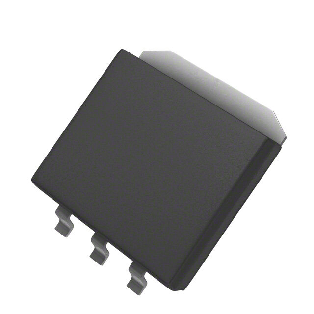
| 产品图片 |
|
| rohs | 符合RoHS无铅 / 符合限制有害物质指令(RoHS)规范要求 |
| 产品系列 | 电源管理 IC,线性稳压器,Texas Instruments UA79M05CKVURG3- |
| 数据手册 | |
| 产品型号 | UA79M05CKVURG3 |
| PSRR/纹波抑制—典型值 | 60 dB |
| 产品种类 | |
| 供应商器件封装 | TO-252-3 |
| 其它名称 | 296-20735-6 |
| 包装 | Digi-Reel® |
| 单位重量 | 328.800 mg |
| 商标 | Texas Instruments |
| 安装类型 | 表面贴装 |
| 安装风格 | SMD/SMT |
| 封装 | Reel |
| 封装/外壳 | TO-252-3,DPak(2 引线+接片),SC-63 |
| 封装/箱体 | TO-252-3 |
| 工作温度 | 0°C ~ 125°C |
| 工厂包装数量 | 2500 |
| 最大工作温度 | + 125 C |
| 最大输入电压 | - 25 V |
| 最小工作温度 | 0 C |
| 最小输入电压 | - 7 V |
| 极性 | Negative |
| 标准包装 | 1 |
| 电压-跌落(典型值) | 1.1V @ 350mA |
| 电压-输入 | -7 V ~ -25 V |
| 电压-输出 | -5V |
| 电流-输出 | 500mA |
| 电流-限制(最小值) | - |
| 稳压器拓扑 | 负,固定式 |
| 稳压器数 | 1 |
| 系列 | UA79M05 |
| 线路调整率 | 50 mV |
| 负载调节 | 100 mV |
| 输出电压 | - 5 V |
| 输出电流 | 0.5 A |
| 输出端数量 | 1 |
| 输出类型 | Fixed |


- 商务部:美国ITC正式对集成电路等产品启动337调查
- 曝三星4nm工艺存在良率问题 高通将骁龙8 Gen1或转产台积电
- 太阳诱电将投资9.5亿元在常州建新厂生产MLCC 预计2023年完工
- 英特尔发布欧洲新工厂建设计划 深化IDM 2.0 战略
- 台积电先进制程称霸业界 有大客户加持明年业绩稳了
- 达到5530亿美元!SIA预计今年全球半导体销售额将创下新高
- 英特尔拟将自动驾驶子公司Mobileye上市 估值或超500亿美元
- 三星加码芯片和SET,合并消费电子和移动部门,撤换高东真等 CEO
- 三星电子宣布重大人事变动 还合并消费电子和移动部门
- 海关总署:前11个月进口集成电路产品价值2.52万亿元 增长14.8%


PDF Datasheet 数据手册内容提取
µ(cid:1)(cid:2)(cid:3)(cid:4)(cid:5)(cid:5) (cid:6)(cid:7)(cid:8)(cid:9)(cid:7)(cid:6) (cid:10)(cid:7)(cid:11)(cid:1)(cid:12)(cid:9)(cid:13)(cid:7)(cid:14)(cid:13)(cid:15)(cid:16)(cid:12)(cid:1)(cid:11)(cid:7) (cid:8)(cid:7)(cid:11)(cid:17)(cid:16)(cid:1)(cid:12)(cid:15)(cid:8)(cid:6) SLVS060K − JUNE 1976 − REVISED APRIL 2005 (cid:1) (cid:1) 3-Terminal Regulators High Power-Dissipation Capability (cid:1) (cid:1) Output Current Up To 500 mA Internal Short-Circuit Current Limiting (cid:1) (cid:1) No External Components Output Transistor Safe-Area Compensation µA79M05...KC (TO-220) PACKAGE µA79M05, µA79M08...KTP PACKAGE (TOP VIEW) (TOP VIEW) OUTPUT UT OUTPUT T P INPUT U INPUT IN COMMON INP COMMON µA79M05...KCS (TO-220) PACKAGE (TOP VIEW) UT OUTPUT P INPUT N COMMON I description/ordering information This series of fixed-negative-voltage integrated-circuit voltage regulators is designed to complement the µA78M00 series in a wide range of applications. These applications include on-card regulation for elimination of noise and distribution problems associated with single-point regulation. Each of these regulators delivers up to 500 mA of output current. The internal current-limiting and thermal-shutdown features of these regulators essentially make them immune to overload. In addition to use as fixed-voltage regulators, these devices can be used with external components to obtain adjustable output voltages and currents, and also as the power-pass element in precision regulators. ORDERING INFORMATION TJ VO((NVO) M) PACKAGE† POARRDT ENRUAMBBLEER MTOAPR-KSIINDGE PowerFLEX (KTP) Reel of 3000 µA79M05CKTPR µA79M05C −−55 TO-220 (KC) Tube of 50 µA79M05CKC 00°°CC ttoo 112255°°CC µAA7799MM0055CC TO-220, short shoulder (KCS) Tube of 20 µA79M05CKCS −8 PowerFLEX (KTP) Reel of 3000 µA79M08CKTPR µA79M08C †Package drawings, standard packing quantities, thermal data, symbolization, and PCB design guidelines are available at www.ti.com/sc/package. Please be aware that an important notice concerning availability, standard warranty, and use in critical applications of TexasInstruments semiconductor products and disclaimers thereto appears at the end of this data sheet. PowerFLEX is a trademark of Texas Instruments. (cid:18)(cid:8)(cid:15)(cid:19)(cid:17)(cid:20)(cid:12)(cid:9)(cid:15)(cid:10) (cid:19)(cid:1)(cid:12)(cid:1) (cid:21)(cid:22)(cid:23)(cid:24)(cid:25)(cid:26)(cid:27)(cid:28)(cid:21)(cid:24)(cid:22) (cid:21)(cid:29) (cid:30)(cid:31)(cid:25)(cid:25)!(cid:22)(cid:28) (cid:27)(cid:29) (cid:24)(cid:23) "(cid:31)#$(cid:21)(cid:30)(cid:27)(cid:28)(cid:21)(cid:24)(cid:22) %(cid:27)(cid:28)!& Copyright 2005, Texas Instruments Incorporated (cid:18)(cid:25)(cid:24)%(cid:31)(cid:30)(cid:28)(cid:29) (cid:30)(cid:24)(cid:22)(cid:23)(cid:24)(cid:25)(cid:26) (cid:28)(cid:24) (cid:29)"!(cid:30)(cid:21)(cid:23)(cid:21)(cid:30)(cid:27)(cid:28)(cid:21)(cid:24)(cid:22)(cid:29) "!(cid:25) (cid:28)’! (cid:28)!(cid:25)(cid:26)(cid:29) (cid:24)(cid:23) (cid:12)!((cid:27)(cid:29) (cid:9)(cid:22)(cid:29)(cid:28)(cid:25)(cid:31)(cid:26)!(cid:22)(cid:28)(cid:29) (cid:29)(cid:28)(cid:27)(cid:22)%(cid:27)(cid:25)% )(cid:27)(cid:25)(cid:25)(cid:27)(cid:22)(cid:28)*& (cid:18)(cid:25)(cid:24)%(cid:31)(cid:30)(cid:28)(cid:21)(cid:24)(cid:22) "(cid:25)(cid:24)(cid:30)!(cid:29)(cid:29)(cid:21)(cid:22)+ %(cid:24)!(cid:29) (cid:22)(cid:24)(cid:28) (cid:22)!(cid:30)!(cid:29)(cid:29)(cid:27)(cid:25)(cid:21)$* (cid:21)(cid:22)(cid:30)$(cid:31)%! (cid:28)!(cid:29)(cid:28)(cid:21)(cid:22)+ (cid:24)(cid:23) (cid:27)$$ "(cid:27)(cid:25)(cid:27)(cid:26)!(cid:28)!(cid:25)(cid:29)& POST OFFICE BOX 655303 • DALLAS, TEXAS 75265 1
µ(cid:1)(cid:2)(cid:3)(cid:4)(cid:5)(cid:5) (cid:6)(cid:7)(cid:8)(cid:9)(cid:7)(cid:6) (cid:10)(cid:7)(cid:11)(cid:1)(cid:12)(cid:9)(cid:13)(cid:7)(cid:14)(cid:13)(cid:15)(cid:16)(cid:12)(cid:1)(cid:11)(cid:7) (cid:8)(cid:7)(cid:11)(cid:17)(cid:16)(cid:1)(cid:12)(cid:15)(cid:8)(cid:6) SLVS060K − JUNE 1976 − REVISED APRIL 2005 schematic COMMON 4.5 kΩ to 6.3 kΩ 1.7 kΩ to 18 kΩ OUTPUT 0.1 Ω 0.2 Ω INPUT Resistor values shown are nominal. absolute maximum ratings over virtual junction temperature range (unless otherwise noted)† Input voltage, V . . . . . . . . . . . . . . . . . . . . . . . . . . . . . . . . . . . . . . . . . . . . . . . . . . . . . . . . . . . . . . . . . . . . . . . . . . . 35 V I Operating virtual junction temperature, T . . . . . . . . . . . . . . . . . . . . . . . . . . . . . . . . . . . . . . . . . . . . . . . . . . . 150°C J Lead temperature 1,6 mm (1/16 inch) from case for 10 seconds . . . . . . . . . . . . . . . . . . . . . . . . . . . . . . . 260°C Storage temperature range, T . . . . . . . . . . . . . . . . . . . . . . . . . . . . . . . . . . . . . . . . . . . . . . . . . . . . −65°C to 150°C stg †Stresses beyond those listed under “absolute maximum ratings” may cause permanent damage to the device. These are stress ratings only, and functional operation of the device at these or any other conditions beyond those indicated under “recommended operating conditions” is not implied. Exposure to absolute-maximum-rated conditions for extended periods may affect device reliability. package thermal data (see Note 1) PACKAGE BOARD θJC θJA θJP‡ PowerFLEX (KTP) High K, JESD 51-5 19°C/W 28°C/W 1.4°C/W TO-220 (KC/KCS) High K, JESD 51-5 17°C/W 19°C/W 3°C/W NOTE 1: Maximum power dissipation is a function of TJ(max), θJA, and TA. The maximum allowable power dissipation at any allowable ambient temperature is PD = (TJ(max) − TA)/θJA. Operating at the absolute maximum TJ of 150°C can affect reliability. ‡For packages with exposed thermal pads, such as QFN, PowerPAD, or PowerFLEX, θJP is defined as the thermal resistance between the die junction and the bottom of the exposed pad. 2 POST OFFICE BOX 655303 • DALLAS, TEXAS 75265
µ(cid:1)(cid:2)(cid:3)(cid:4)(cid:5)(cid:5) (cid:6)(cid:7)(cid:8)(cid:9)(cid:7)(cid:6) (cid:10)(cid:7)(cid:11)(cid:1)(cid:12)(cid:9)(cid:13)(cid:7)(cid:14)(cid:13)(cid:15)(cid:16)(cid:12)(cid:1)(cid:11)(cid:7) (cid:8)(cid:7)(cid:11)(cid:17)(cid:16)(cid:1)(cid:12)(cid:15)(cid:8)(cid:6) SLVS060K − JUNE 1976 − REVISED APRIL 2005 recommended operating conditions MIN MAX UNIT µA79M05C −7 −25 VVII IInnppuutt vvoollttaaggee µA79M08C −10.5 −25 VV IO Output current 500 mA TJ Operating virtual junction temperature 0 125 °C electrical characteristics at specified virtual junction temperature, V = −10 V, I = 350 mA, T = 25°C I O J (unless otherwise noted) µA79M05C PPAARRAAMMEETTEERR TTEESSTT CCOONNDDIITTIIOONNSS†† UUNNIITT MIN TYP MAX −4.8 −5 −5.2 OOuuttppuutt vvoollttaaggee VVII == −−77 VV ttoo −−2255 VV,, IIOO == 55 mmAA ttoo 335500 mmAA TJ = 0°C to 125°C −4.75 −5.25 VV VI = −7 V to −25 V 7 50 IInnppuutt vvoollttaaggee rreegguullaattiioonn mmVV VI = −8 V to −18 V 3 30 VVII == −−88 VV ttoo −−1188 VV,, IO = 100 mA, TJ = 0°C to 125°C 50 RRiippppllee rreejjeeccttiioonn ddBB f = 120 Hz IO = 300 mA 54 60 IO = 5 mA to 500 mA 75 100 OOuuttppuutt vvoollttaaggee rreegguullaattiioonn mmVV IO = 5 mA to 350 mA 50 Temperature coefficient of output voltage IO = 5 mA, TJ = 0°C to 125°C −0.4 mV/°C Output noise voltage f = 10 Hz to 100 kHz 125 µV Dropout voltage 1.1 V Bias current 1 2 mA VI = −8 V to −18 V, TJ = 0°C to 125°C 0.4 BBiiaass ccuurrrreenntt cchhaannggee mmAA IO = 5 mA to 350 mA, TJ = 0°C to 125°C 0.4 Short-circuit output current VI = −30 V 140 mA Peak output current 0.65 A †Pulse-testing techniques maintain TJ as close to TA as possible. Thermal effects must be taken into account separately. All characteristics are measured with a 2-µF capacitor across the input and a 1-µF capacitor across the output. POST OFFICE BOX 655303 • DALLAS, TEXAS 75265 3
µ(cid:1)(cid:2)(cid:3)(cid:4)(cid:5)(cid:5) (cid:6)(cid:7)(cid:8)(cid:9)(cid:7)(cid:6) (cid:10)(cid:7)(cid:11)(cid:1)(cid:12)(cid:9)(cid:13)(cid:7)(cid:14)(cid:13)(cid:15)(cid:16)(cid:12)(cid:1)(cid:11)(cid:7) (cid:8)(cid:7)(cid:11)(cid:17)(cid:16)(cid:1)(cid:12)(cid:15)(cid:8)(cid:6) SLVS060K − JUNE 1976 − REVISED APRIL 2005 electrical characteristics at specified virtual junction temperature, V = −19 V, I = 350 mA, T = 25°C I O J (unless otherwise noted) µA79M08C PPAARRAAMMEETTEERR TTEESSTT CCOONNDDIITTIIOONNSS†† UUNNIITT MIN TYP MAX −7.7 −8 −8.3 OOuuttppuutt vvoollttaaggee VVII == −−1100..55 VV ttoo −−2255 VV,, IIOO == 55 mmAA ttoo 335500 mmAA TJ = 0°C to 125°C −7.6 −8.4 VV VI = −10.5 V to −25 V 8 80 IInnppuutt vvoollttaaggee rreegguullaattiioonn mmVV VI = −11 V to −21 V 4 50 VVII == −−1111..55 VV ttoo −−2211..55 VV,, IO = 100 mA, TJ = 0°C to 125°C 50 RRiippppllee rreejjeeccttiioonn ddBB f = 120 Hz IO = 300 mA 54 59 IO = 5 mA to 500 mA 90 160 OOuuttppuutt vvoollttaaggee rreegguullaattiioonn mmVV IO = 5 mA to 350 mA 60 Temperature coefficient of output voltage IO = 5 mA, TJ = 0°C to 125°C −0.6 mV/°C Output noise voltage f = 10 Hz to 100 kHz 200 µV Dropout voltage IO = 5 mA 1.1 V Bias current 1 2 mA VI = −10.5 V to −25 V, TJ = 0°C to 125°C 0.4 BBiiaass ccuurrrreenntt cchhaannggee mmAA IO = 5 mA to 350 mA, TJ = 0°C to 125°C 0.4 Short-circuit output current VI = −30 V 140 mA Peak output current 0.65 A †Pulse-testing techniques maintain TJ as close to TA as possible. Thermal effects must be taken into account separately. All characteristics are measured with a 2-µF capacitor across the input and a 1-µF capacitor across the output. 4 POST OFFICE BOX 655303 • DALLAS, TEXAS 75265
PACKAGE OPTION ADDENDUM www.ti.com 6-Feb-2020 PACKAGING INFORMATION Orderable Device Status Package Type Package Pins Package Eco Plan Lead/Ball Finish MSL Peak Temp Op Temp (°C) Device Marking Samples (1) Drawing Qty (2) (6) (3) (4/5) UA79M05CKCS ACTIVE TO-220 KCS 3 50 Pb-Free SN N / A for Pkg Type 0 to 125 UA79M05C (RoHS) UA79M05CKVURG3 ACTIVE TO-252 KVU 3 2500 Green (RoHS SN Level-3-260C-168 HR 0 to 125 79M05C & no Sb/Br) UA79M08CKVURG3 ACTIVE TO-252 KVU 3 2500 Green (RoHS SN Level-3-260C-168 HR 0 to 125 79M08C & no Sb/Br) (1) The marketing status values are defined as follows: ACTIVE: Product device recommended for new designs. LIFEBUY: TI has announced that the device will be discontinued, and a lifetime-buy period is in effect. NRND: Not recommended for new designs. Device is in production to support existing customers, but TI does not recommend using this part in a new design. PREVIEW: Device has been announced but is not in production. Samples may or may not be available. OBSOLETE: TI has discontinued the production of the device. (2) RoHS: TI defines "RoHS" to mean semiconductor products that are compliant with the current EU RoHS requirements for all 10 RoHS substances, including the requirement that RoHS substance do not exceed 0.1% by weight in homogeneous materials. Where designed to be soldered at high temperatures, "RoHS" products are suitable for use in specified lead-free processes. TI may reference these types of products as "Pb-Free". RoHS Exempt: TI defines "RoHS Exempt" to mean products that contain lead but are compliant with EU RoHS pursuant to a specific EU RoHS exemption. Green: TI defines "Green" to mean the content of Chlorine (Cl) and Bromine (Br) based flame retardants meet JS709B low halogen requirements of <=1000ppm threshold. Antimony trioxide based flame retardants must also meet the <=1000ppm threshold requirement. (3) MSL, Peak Temp. - The Moisture Sensitivity Level rating according to the JEDEC industry standard classifications, and peak solder temperature. (4) There may be additional marking, which relates to the logo, the lot trace code information, or the environmental category on the device. (5) Multiple Device Markings will be inside parentheses. Only one Device Marking contained in parentheses and separated by a "~" will appear on a device. If a line is indented then it is a continuation of the previous line and the two combined represent the entire Device Marking for that device. (6) Lead/Ball Finish - Orderable Devices may have multiple material finish options. Finish options are separated by a vertical ruled line. Lead/Ball Finish values may wrap to two lines if the finish value exceeds the maximum column width. Important Information and Disclaimer:The information provided on this page represents TI's knowledge and belief as of the date that it is provided. TI bases its knowledge and belief on information provided by third parties, and makes no representation or warranty as to the accuracy of such information. Efforts are underway to better integrate information from third parties. TI has taken and continues to take reasonable steps to provide representative and accurate information but may not have conducted destructive testing or chemical analysis on incoming materials and chemicals. TI and TI suppliers consider certain information to be proprietary, and thus CAS numbers and other limited information may not be available for release. Addendum-Page 1
PACKAGE OPTION ADDENDUM www.ti.com 6-Feb-2020 In no event shall TI's liability arising out of such information exceed the total purchase price of the TI part(s) at issue in this document sold by TI to Customer on an annual basis. Addendum-Page 2
PACKAGE MATERIALS INFORMATION www.ti.com 29-May-2013 TAPE AND REEL INFORMATION *Alldimensionsarenominal Device Package Package Pins SPQ Reel Reel A0 B0 K0 P1 W Pin1 Type Drawing Diameter Width (mm) (mm) (mm) (mm) (mm) Quadrant (mm) W1(mm) UA79M05CKVURG3 TO-252 KVU 3 2500 330.0 16.4 6.9 10.5 2.7 8.0 16.0 Q2 UA79M08CKVURG3 TO-252 KVU 3 2500 330.0 16.4 6.9 10.5 2.7 8.0 16.0 Q2 PackMaterials-Page1
PACKAGE MATERIALS INFORMATION www.ti.com 29-May-2013 *Alldimensionsarenominal Device PackageType PackageDrawing Pins SPQ Length(mm) Width(mm) Height(mm) UA79M05CKVURG3 TO-252 KVU 3 2500 340.0 340.0 38.0 UA79M08CKVURG3 TO-252 KVU 3 2500 340.0 340.0 38.0 PackMaterials-Page2
PACKAGE OUTLINE KCS0003B TO-220 - 19.65 mm max height SCALE 0.850 TO-220 4.7 4.4 10.36 1.32 2.9 8.55 9.96 1.22 2.6 8.15 6.5 (6.3) 6.1 ( 3.84) 12.5 12.1 19.65 MAX 9.25 9.05 3X 3.9 MAX 13.12 12.70 1 3 0.90 0.47 3X 0.77 0.34 2.79 2X 2.54 2.59 1.36 3X 1.23 5.08 4222214/B 08/2018 NOTES: 1. Dimensions are in millimeters. Any dimension in brackets or parenthesis are for reference only. Dimensioning and tolerancing per ASME Y14.5M. 2. This drawing is subject to change without notice. 3. Reference JEDEC registration TO-220. www.ti.com
EXAMPLE BOARD LAYOUT KCS0003B TO-220 - 19.65 mm max height TO-220 0.07 MAX 2X (1.7) ALL AROUND 3X (1.2) METAL 2X SOLDER MASK OPENING (1.7) 1 2 3 0.07 MAX R (0.05) ALL AROUND (2.54) SOLDER MASK (5.08) OPENING LAND PATTERN EXAMPLE NON-SOLDER MASK DEFINED SCALE:15X 4222214/B 08/2018 www.ti.com
None
PACKAGE OUTLINE KVU0003A TO-252 - 2.52 mm max height SCALE 1.500 TO-252 10.41 9.40 6.22 1.27 B A 5.97 0.89 1 2.29 6.70 2 5.460 6.35 4.58 4.953 3 0.890 3X 1.02 0.635 OPTIONAL NOTE 3 0.61 0.25 C A B 0.61 2.52 MAX C 0.46 0.61 0.46 SEE DETAIL A 5.21 MIN 3 4.32 2 4 MIN 1 EXPOSED 0.51 THERMAL PAD GAGE PLANE NOTE 3 0.13 0 -8 1.78 0.00 1.40 DETA 7.000AIL A TYPICAL 4218915/A 02/2017 NOTES: 1. All linear dimensions are in millimeters. Any dimensions in parenthesis are for reference only. Dimensioning and tolerancing per ASME Y14.5M. 2. This drawing is subject to change without notice. 3. Shape may vary per different assembly sites. 4. Reference JEDEC registration TO-252. www.ti.com
EXAMPLE BOARD LAYOUT KVU0003A TO-252 - 2.52 mm max height TO-252 2X (2.75) (6.15) 2X (1) 1 4 SYMM (4.58) (5.55) 3 (R0.05) TYP (4.2) (2.5) PKG LAND PATTERN EXAMPLE EXPOSED METAL SHOWN SCALE:6X 0.07 MAX 0.07 MIN ALL AROUND ALL AROUND EXPOSED METAL EXPOSED METAL SOLDER MASK METAL METAL UNDER SOLDER MASK OPENING SOLDER MASK OPENING NON SOLDER MASK SOLDER MASK DEFINED DEFINED SOLDER MASK DETAILS NOT TO SCALE 4218915/A 02/2017 NOTES: (continued) 5. This package is designed to be soldered to a thermal pad on the board. For more information, see Texas Instruments literature numbers SLMA002(www.ti.com/lit/slm002) and SLMA004 (www.ti.com/lit/slma004). 6. Vias are optional depending on application, refer to device data sheet. It is recommended that vias under paste be filled, plugged or tented. www.ti.com
EXAMPLE STENCIL DESIGN KVU0003A TO-252 - 2.52 mm max height TO-252 (1.18) TYP 2X (2.75) 2X (1) (0.14) 1 (R0.05) (1.33) TYP SYMM (4.58) 4 3 20X (1.13) (4.2) 20X (0.98) PKG SOLDER PASTE EXAMPLE BASED ON 0.125 mm THICK STENCIL EXPOSED PAD 65% PRINTED SOLDER COVERAGE BY AREA SCALE:8X 4218915/A 02/2017 NOTES: (continued) 7. Laser cutting apertures with trapezoidal walls and rounded corners may offer better paste release. IPC-7525 may have alternate design recommendations. 8. Board assembly site may have different recommendations for stencil design. www.ti.com
IMPORTANTNOTICEANDDISCLAIMER TI PROVIDES TECHNICAL AND RELIABILITY DATA (INCLUDING DATASHEETS), DESIGN RESOURCES (INCLUDING REFERENCE DESIGNS), APPLICATION OR OTHER DESIGN ADVICE, WEB TOOLS, SAFETY INFORMATION, AND OTHER RESOURCES “AS IS” AND WITH ALL FAULTS, AND DISCLAIMS ALL WARRANTIES, EXPRESS AND IMPLIED, INCLUDING WITHOUT LIMITATION ANY IMPLIED WARRANTIES OF MERCHANTABILITY, FITNESS FOR A PARTICULAR PURPOSE OR NON-INFRINGEMENT OF THIRD PARTY INTELLECTUAL PROPERTY RIGHTS. These resources are intended for skilled developers designing with TI products. You are solely responsible for (1) selecting the appropriate TI products for your application, (2) designing, validating and testing your application, and (3) ensuring your application meets applicable standards, and any other safety, security, or other requirements. These resources are subject to change without notice. TI grants you permission to use these resources only for development of an application that uses the TI products described in the resource. Other reproduction and display of these resources is prohibited. No license is granted to any other TI intellectual property right or to any third party intellectual property right. TI disclaims responsibility for, and you will fully indemnify TI and its representatives against, any claims, damages, costs, losses, and liabilities arising out of your use of these resources. TI’s products are provided subject to TI’s Terms of Sale (www.ti.com/legal/termsofsale.html) or other applicable terms available either on ti.com or provided in conjunction with such TI products. TI’s provision of these resources does not expand or otherwise alter TI’s applicable warranties or warranty disclaimers for TI products. Mailing Address: Texas Instruments, Post Office Box 655303, Dallas, Texas 75265 Copyright © 2020, Texas Instruments Incorporated