ICGOO在线商城 > 集成电路(IC) > PMIC - 稳压器 - 线性 > REG104FA-2.5KTTT
 Datasheet下载
- 型号: REG104FA-2.5KTTT
- 制造商: Texas Instruments
- 库位|库存: xxxx|xxxx
- 要求:
| 数量阶梯 | 香港交货 | 国内含税 |
| +xxxx | $xxxx | ¥xxxx |
查看当月历史价格
查看今年历史价格
REG104FA-2.5KTTT产品简介:
ICGOO电子元器件商城为您提供REG104FA-2.5KTTT由Texas Instruments设计生产,在icgoo商城现货销售,并且可以通过原厂、代理商等渠道进行代购。 REG104FA-2.5KTTT价格参考¥20.94-¥38.90。Texas InstrumentsREG104FA-2.5KTTT封装/规格:PMIC - 稳压器 - 线性, Linear Voltage Regulator IC Positive Fixed 1 Output 2.5V 1A DDPAK/TO-263-5。您可以下载REG104FA-2.5KTTT参考资料、Datasheet数据手册功能说明书,资料中有REG104FA-2.5KTTT 详细功能的应用电路图电压和使用方法及教程。
Texas Instruments(德州仪器)的REG104FA-2.5KTTT是一款PMIC(电源管理集成电路)中的线性稳压器。其主要应用场景包括以下方面:

 1. 低功耗设备
   - REG104FA-2.5KTTT具有低静态电流和高精度输出电压的特点,适合用于对功耗要求严格的便携式设备,例如手持终端、传感器模块和物联网(IoT)设备。

 2. 嵌入式系统
   - 在嵌入式系统中,该稳压器可以为微控制器(MCU)、数字信号处理器(DSP)和其他低电压组件提供稳定的2.5V电源。其线性稳压特性能够有效减少电磁干扰(EMI),提高系统的稳定性。

 3. 通信设备
   - 此型号适用于需要稳定电源的通信模块,如蓝牙、Wi-Fi、Zigbee等无线通信芯片组。它能够确保在不同负载条件下输出电压的稳定性,从而优化通信性能。

 4. 医疗电子
   - 在医疗设备中,例如可穿戴健康监测设备、脉搏血氧仪或便携式诊断工具,REG104FA-2.5KTTT可以提供精确且可靠的电源供应,支持设备长时间运行并保持测量精度。

 5. 工业自动化
   - 工业环境中,该稳压器可用于传感器接口、数据采集模块和控制单元等场景。其宽输入电压范围和良好的热性能使其能够在恶劣环境下稳定工作。

 6. 消费类电子产品
   - 该器件也可应用于消费类电子产品,如智能音箱、遥控器和电子玩具等,为内部电路提供高效、稳定的电源支持。

总之,REG104FA-2.5KTTT凭借其高精度、低噪声和紧凑封装的优势,广泛适用于各种需要稳定低压电源的应用场合,尤其是在对能效和空间有限制的场景中表现尤为突出。
| 参数 | 数值 |
| 产品目录 | 集成电路 (IC)半导体 |
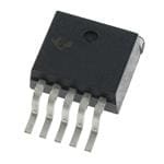
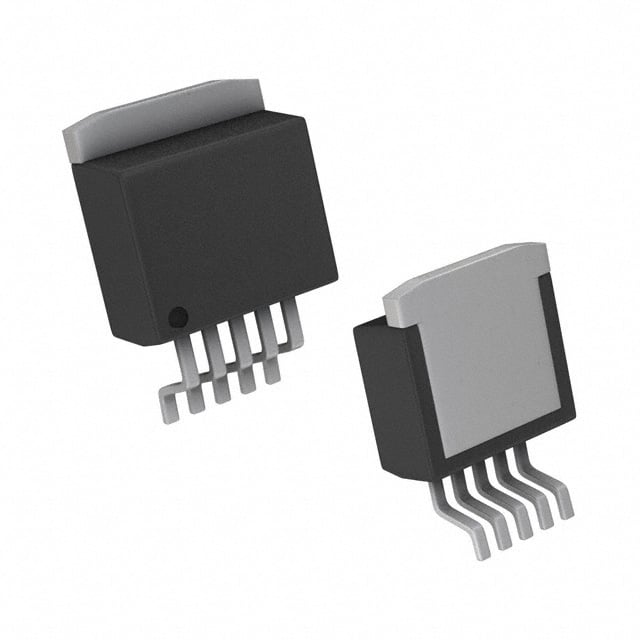
| 描述 | IC REG LDO 2.5V 1A DDPAK低压差稳压器 DMOS 1A LDO Reg |
| 产品分类 | |
| 品牌 | Texas Instruments |
| 产品手册 | |
| 产品图片 |
|
| rohs | 符合RoHS无铅 / 符合限制有害物质指令(RoHS)规范要求 |
| 产品系列 | 电源管理 IC,低压差稳压器,Texas Instruments REG104FA-2.5KTTT- |
| 数据手册 | |
| 产品型号 | REG104FA-2.5KTTT |
| 产品目录页面 | |
| 产品种类 | 低压差稳压器 |
| 供应商器件封装 | DDPAK/TO-263-5 |
| 其它名称 | 296-15999-1 |
| 包装 | 剪切带 (CT) |
| 单位重量 | 1.456 g |
| 参考电压 | 1.295 V |
| 商标 | Texas Instruments |
| 安装类型 | 表面贴装 |
| 安装风格 | SMD/SMT |
| 封装 | Tube |
| 封装/外壳 | TO-263-6,D²Pak(5 引线+接片),TO-263BA |
| 封装/箱体 | TO-263-5 |
| 工作温度 | -40°C ~ 85°C |
| 工厂包装数量 | 50 |
| 最大工作温度 | + 85 C |
| 最大输入电压 | 15 V |
| 最小工作温度 | - 40 C |
| 最小输入电压 | + 2.1 V |
| 标准包装 | 1 |
| 电压-跌落(典型值) | - |
| 电压-输入 | 最高 15V |
| 电压-输出 | 2.5V |
| 电压调节准确度 | 2 % |
| 电流-输出 | 1A |
| 电流-限制(最小值) | 1.2A |
| 稳压器拓扑 | 正,固定式 |
| 稳压器数 | 1 |
| 系列 | REG104-25 |
| 输入偏压电流—最大 | 0.6 mA |
| 输出电压 | 2.5 V |
| 输出电流 | 1 A |
| 输出端数量 | 1 Output |
| 输出类型 | Fixed |


- 商务部:美国ITC正式对集成电路等产品启动337调查
- 曝三星4nm工艺存在良率问题 高通将骁龙8 Gen1或转产台积电
- 太阳诱电将投资9.5亿元在常州建新厂生产MLCC 预计2023年完工
- 英特尔发布欧洲新工厂建设计划 深化IDM 2.0 战略
- 台积电先进制程称霸业界 有大客户加持明年业绩稳了
- 达到5530亿美元!SIA预计今年全球半导体销售额将创下新高
- 英特尔拟将自动驾驶子公司Mobileye上市 估值或超500亿美元
- 三星加码芯片和SET,合并消费电子和移动部门,撤换高东真等 CEO
- 三星电子宣布重大人事变动 还合并消费电子和移动部门
- 海关总署:前11个月进口集成电路产品价值2.52万亿元 增长14.8%


PDF Datasheet 数据手册内容提取
REG104 REG104 REG104 SBVS025G – SEPTEMBER 2001 – REVISED SEPTEMBER 2005 DMOS 1A Low-Dropout Regulator FEATURES DESCRIPTION (cid:1) NEW DMOS TOPOLOGY: The REG104 is a family of low-noise, low-dropout linear Ultra Low Dropout Voltage: regulators with low ground pin current. Its new DMOS topol- 230mV typ at 1A and 3.3V Output ogy provides significant improvement over previous designs, Output Capacitor NOT Required for Stability including low dropout voltage (only 230mV typ at full load), (cid:1) FAST TRANSIENT RESPONSE and better transient performance. In addition, no output capacitor is required for stability, unlike conventional low (cid:1) VERY LOW NOISE: 33µV RMS dropout regulators that are difficult to compensate and (cid:1) HIGH ACCURACY: ±2% max require expensive low ESR capacitors greater than 1µF. (cid:1) HIGH EFFICIENCY: Typical ground pin current is only 1.7mA (at I = 1A) and OUT I = 1.7mA at I = 1A drops to 0.5µA in not enabled mode. Unlike regulators with GND OUT µ Not Enabled: I = 0.5 A PNP pass devices, quiescent current remains relatively con- GND (cid:1) 2.5V, 2.7V, 3.0V, 3.3V, 5.0V AND stant over load variations and under dropout conditions. ADJUSTABLE OUTPUT VERSIONS The REG104 has very low output noise (typically 33µV RMS (cid:1) THERMAL PROTECTION for VOUT = 3.3V with CNR = 0.01µF), making it ideal for use (cid:1) SMALL SURFACE-MOUNT PACKAGES: in portable communications equipment. On-chip trimming results in high output voltage accuracy. Accuracy is main- SOT223-5, DDPAK-5 tained over temperature, line, and load variations. Key pa- rameters are tested over the specified temperature range APPLICATIONS (–40°C to +85°C). (cid:1) PORTABLE COMMUNICATION DEVICES The REG104 is well protected—internal circuitry provides a current limit which protects the load from damage. Thermal (cid:1) BATTERY-POWERED EQUIPMENT protection circuitry keeps the chip from being damaged by (cid:1) MODEMS excessive temperature. The REG104 is available in the (cid:1) BAR-CODE SCANNERS DDPAK-5 and the SOT223-5. (cid:1) BACKUP POWER SUPPLIES Enable Enable V V V V IN OUT IN OUT + 0.1µF (FixReEdG V1o0lt4age + COUT(1) + 0.1µF REG104-A R1 + COUT(1) Versions) Adj NR Gnd Gnd R2 NR = Noise Reduction NOTE: (1) Optional. Please be aware that an important notice concerning availability, standard warranty, and use in critical applications of Texas Instruments semiconductor products and disclaimers thereto appears at the end of this data sheet. All trademarks are the property of their respective owners. PRODUCTION DATA information is current as of publication date. Copyright © 2001-2005, Texas Instruments Incorporated Products conform to specifications per the terms of Texas Instruments standard warranty. Production processing does not necessarily include testing of all parameters. www.ti.com
ABSOLUTE MAXIMUM RATINGS(1) ELECTROSTATIC Supply Input Voltage, VIN.......................................................–0.3V to 16V DISCHARGE SENSITIVITY Enable Input Voltage, V .......................................................–0.3V to V EN IN Feedback Voltage, V ........................................................–0.3V to 6.0V NR Pin Voltage, V F..B...........................................................–0.3V to 6.0V This integrated circuit can be damaged by ESD. Texas Instru- NR Output Short-Circuit Duration......................................................Indefinite ments recommends that all integrated circuits be handled with Operating Temperature Range.......................................–55°C to +125°C appropriate precautions. Failure to observe proper handling Storage Temperature Range..........................................–65°C to +150°C Junction Temperature.....................................................–55°C to +150°C and installation procedures can cause damage. Lead Temperature (soldering, 3s, SOT, and DDPAK)...................+240°C ESD damage can range from subtle performance degradation ESD Rating: HBM (V to GND).....................................................1.5kV OUT HBM (All other pins)........................................................2kV to complete device failure. Precision integrated circuits may be CDM..............................................................................500V more susceptible to damage because very small parametric NOTE: (1) Stresses above these ratings may cause permanent damage. changes could cause the device not to meet its published Exposure to absolute maximum conditions for extended periods may degrade specifications. device reliability. PACKAGE/ORDERING INFORMATION(1) PRODUCT V OUT REG104xx-yyyy/zzz XX is package designator. YYYY is typical output voltage (5 = 5.0V, 2.85 = 2.85V, A = Adjustable). ZZZ is package quantity. (1) For the most current package and ordering information, see the Package Option Addendum at the end of this document, or see the TI website at www.ti.com. PIN CONFIGURATIONS Top View DDPAK-5 SOT223-5 Tab is Gnd Tab is Gnd 1 2 3 4 5 1 2 3 4 5 VO Gnd VIN V Gnd Enable NR/Adjust(1) Enable IN V NR/Adjust(1) OUT (KTT Package) (DCQ Package) NOTE: (1) For REG104A-A: voltage setting resistor pin. All other models: noise reduction capacitor pin. REG104 2 SBVS025G
ELECTRICAL CHARACTERISTICS ° ° Boldface limits apply over the specified temperature range, T = –40 C to +85 C J At T = +25°C, V = V + 1V (V = 3.0V for REG104-A), V = 2V, I = 10mA, C = 0.01µF, and C = 0.1µF(1), unless otherwise noted. J IN OUT OUT ENABLE OUT NR OUT REG104GA REG104FA PARAMETER CONDITION MIN TYP MAX UNITS OUTPUT VOLTAGE Output Voltage Range V OUT REG104-2.5 2.5 V REG104-2.7 2.7 V REG104-3.0 3.0 V REG104-3.3 3.3 V REG104-5 5 V REG104-A V 5.5 V REF Reference Voltage V 1.295 V REF Adjust Pin Current I 0.2 1 µA ADJ Accuracy ±0.5 ±2 % T = –40°C to +85°C ±3.0 % vsJ Temperature dV /dT T = –40°C to +85°C 70 ppm/°C OUT J vs Line and Load I = 10mA to 1A, V = (V + 0.7V) to 15V ±0.5 ±2.5 % T = –40°C to +85°C OUT V = (V IN+ 0.9VO)U tTo 15V ±3.5 % J IN OUT DC DROPOUT VOLTAGE(2, 3) V I = 10mA 3 25 mV DROP OUT For all models except 5V I = 1A 230 400 mV OUT For 5V model I = 1A 320 500 mV OUT For all models except 5V I = 1A 480 mV T = –40°C to +85°C OUT J For 5V models I = 1A 580 mV T = –40°C to +85°C OUT J VOLTAGE NOISE f = 10Hz to 100kHz V n Without C (all models) C = 0, C = 0 35µV /V • V µV NR NR OUT RMS OUT RMS With C (all fixed voltage models) C = 0.01µF, C = 10µF 10µV /V • V µV NR NR OUT RMS OUT RMS OUTPUT CURRENT Current Limit(4) I 1.2 1.7 2.1 A T = –40°C to +85°C CL 1.0 2.2 A J RIPPLE REJECTION f = 120Hz 65 dB ENABLE CONTROL V High (output enabled) V 2 V V ENABLE ENABLE IN V Low (output disabled) –0.2 0.5 V ENABLE I High (output enabled) I V = 2V to V , V = 2.1V to 6.5(5) 1 100 nA ENABLE ENABLE ENABLE IN IN I Low (output disabled) V = 0V to 0.5V 2 100 nA ENABLE ENABLE Output Disable Time 50 µs Output Enable Softstart Time 1.5 ms THERMAL SHUTDOWN Junction Temperature Shutdown 150 °C Reset from Shutdown 130 °C GROUND PIN CURRENT Ground Pin Current I I = 10mA 0.5 0.7 mA GND OUT I = 1A 1.7 1.8 mA OUT Enable Pin Low V ≤ 0.5V 0.5 µA ENABLE INPUT VOLTAGE V IN Operating Input Voltage Range(6) 2.1 15 V Specified Input Voltage Range V > 2.7V V + 0.7 15 V T = –40°C to +85°C VIN > 2.9V VOUT + 0.9 15 V J IN OUT TEMPERATURE RANGE Specified Range T –40 +85 °C J Operating Range –55 +125 °C Storage Range –65 +150 °C Thermal Resistance DDPAK-5 Surface Mount θ Junction-to-Case 4 °C/W JC SOT223-5 Surface Mount θ Junction-to-Case 15 °C/W JC NOTES: (1) The REG104 does not require a minimum output capacitor for stability. However, transient response can be improved with proper capacitor selection. (2) Dropout voltage is defined as the input voltage minus the output voltage that produces a 2% change in the output voltage from the value at V = V + 1V IN OUT at fixed load. (3) Not applicable for V less than 2.7V. OUT (4) Current limit is the output current that produces a 15% change in output voltage from V = V + 1V and I = 10mA. IN OUT OUT (5) For V > 6.5V, see typical characteristic V vs I . IN ENABLE ENABLE (6) The REG104 no longer regulates when V < V + V . In drop-out or when the input voltage is between 2.7V and 2.1V, the impedance from V IN OUT DROP (MAX) IN to V is typically less than 1Ω at T = +25°C. See typical characteristic Output Voltage Change vs V . OUT J IN REG104 3 SBVS025G
TYPICAL CHARACTERISTICS For all models, at T = +25°C and V = 2V, unless otherwise noted. J ENABLE OUTPUT VOLTAGE CHANGE vs I OUT (V = V + 1V, Output Voltage % Change IN OUT Referred to IOUT = 10mA at +25°C) DC DROPOUT VOLTAGE vs IOUT 0.8 350 0.6 oltage Change (%) ––0000....04224 +125°C +25°C pout Voltage (mV) 322105050000 +125°C +2–55°5C°C V o ut –0.6 Dr 100 Outp –0.8 –55°C DC 50 –1 –1.2 0 0 100 200 300 400 500 600 700 800 900 1000 0 200 400 600 800 1000 Output Current (mA) IOUT (mA) OUTPUT VOLTAGE CHANGE vs V OUTPUT VOLTAGE CHANGE vs I IN OUT (Output Voltage % Change Referred to (Output Voltage % Change Referred to V = V + 1V at I = 10mA) I = 10mA at +25°C) IN OUT OUT OUT 0.5 0.6 I = 10mA I = 200mA OUT OUT 0.4 I = 10mA %) 0 0.2 OUT Change ( –0.5 IOUT = 1000mA age (%) –0.20 IOUT = 200mA ut Voltage –1 Output Volt ––00..46 IOUT = 1000mA p Out –1.5 –0.8 –1 –2 –1.2 0 2 4 6 8 10 12 –60 –40 –20 0 20 40 60 80 100 120 Input Voltage Above V (V) Temperature (°C) OUT LINE REGULATION vs TEMPERATURE DC DROPOUT VOLTAGE vs TEMPERATURE (V = V + 1V to 16V) IN OUT 350 0.5 300 e (mV) 250 IOUT = 1000mA nge (%) 0.4 g a a h 0.3 opout Volt 210500 Voltage C 0.2 IOUT = 10mA DC Dr 100 IOUT = 200mA Output 0.1 50 I = 200mA I = 10mA OUT OUT 0 0 –75 –50 –25 0 25 50 75 100 125 –75 –50 –25 0 25 50 75 100 125 Temperature (°C) Temperature (°C) REG104 4 SBVS025G
TYPICAL CHARACTERISTICS (Cont.) For all models, at T = +25°C and V = 2V, unless otherwise noted. J ENABLE LOAD TRANSIENT RESPONSE LINE TRANSIENT RESPONSE REG104-3.3 REG104-3.3 500mV/div COUT = 0 VOUT 50mV/div COUT = 0 IOUT = 200mA VOUT mV/div COUT = 10µF VOUT mV/div COUT = 10µF VOUT 500 50 1A I 6V V LOAD IN 10mA 5V 10µs/div 50µs/div LOAD TRANSIENT RESPONSE LOAD TRANSIENT RESPONSE REG104–A REG104–A mV/div CFB = 0.01µF, VOUT = 3.3V V/div Load = 200mA, CFB = 0.01µF, VOUT = 3.3V 0 C = 0 m 0 OUT 0 C = 0 5 5 OUT 500mV/div COUT = 10µF 50mV/div COUT = 10µF 1A I 6V V LOAD IN 10mA 5V 10µs/div 50µs/div LOAD REGULATION vs TEMPERATURE (V = V + 1V and 10mA < I < 1000mA) OUTPUT NOISE DENSITY IN OUT OUT 0.5 10 5 e (%) 0.4 Hz) 2 ang √V/ 1 h 0.3 µ ge C sity ( 0.5 a n 0.2 put Volt 0.2 oise De 0.1 CCNORU T= = 0 0 Out 0.1 N 0.05 C = 0.01µF 0.02 CNR = 10µF OUT 0 0.01 –60 –40 –20 0 20 40 60 80 100 120 10 100 1000 10000 100,000 Temperature (°C) Frequency (Hz) REG104 5 SBVS025G
TYPICAL CHARACTERISTICS (Cont.) For all models, at T = +25°C and V = 2V, unless otherwise noted. J ENABLE GROUND PIN CURRENT, NOT ENABLED GROUND PIN CURRENT vs TEMPERATURE vs TEMPERATURE 1.8 3 IOUT = 1000mA VENABLE = 0V 1.6 2.5 1.4 2 A) 1.2 A) m µ I (GND 1 I (GND 1.5 IOUT = 200mA 1 0.8 0.5 0.6 I = 10mA OUT 0.4 0 –60 –40 –20 0 20 40 60 80 100 120 –75 –50 –25 0 25 50 75 100 125 Temperature (°C) Temperature (°C) GROUND PIN CURRENT vs IOUT IADJUST vs TEMPERATURE 1.6 0.28 REG104-A 0.26 1.4 A) µ 0.24 1.2 nt ( mA) urre 0.22 I(GND 0.18 st Pin C 0.20 dju 0.18 A 0.6 0.16 0.4 0.14 1 10 100 1000 –60 –40 –20 0 20 40 60 80 100 120 140 I (mA) Temperature (°C) OUT CURRENT LIMIT vs TEMPERATURE RIPPLE REJECTION vs FREQUENCY 1850 70 V = V • 0.90 OUT OUT-NOMINAL 1800 60 Current Limit (mA) 111776505000 VOUT = 1V Ripple Rejection (dB) 5400 COUTC =O U1T0 =µ F0 30 1600 1550 20 –60 –40 –20 0 20 40 60 80 100 120 10 100 1k 10k 100k Temperature (°C) Frequency (Hz) REG104 6 SBVS025G
TYPICAL CHARACTERISTICS (Cont.) For all models, at T = +25°C and V = 2V, unless otherwise noted. J ENABLE RIPPLE REJECTION vs I SOFT START OUT 75 V = 3Vp-p, f = 120Hz RIPPLE 70 v B) 65 V/di VOUT d 1 n ( ctio 60 e ej R 55 e pl Rip 50 45 2V V ENABLE 40 0 0 200 400 600 800 1000 250µs/div I (mA) OUT OUTPUT DISABLE TIME OUTPUT VOLTAGE DRIFT HISTOGRAM 45 C = 0 OUT 40 1V/div VOUT s (%) 3350 nit 25 U nt of 20 e c 15 er 2V P 10 VENABLE 5 0 0 10µs/div 40 45 50 55 60 65 70 75 80 85 90 V Drift (ppm/°C) OUT OUTPUT VOLTAGE ACCURACY HISTOGRAM 60 50 %) s ( 40 nit U of 30 nt e c 20 er P 10 0 –1 –0.8 –0.6 –0.4 –0.2 0 0.2 0.4 0.6 0.8 1 Error (%) REG104 7 SBVS025G
BASIC OPERATION None of the versions require an output capacitor for regulator stability. The REG104 will accept any output capacitor type The REG104 series is a family of LDO (Low DropOut) linear less than 1µF. For capacitance values larger than 1µF the regulators. The family includes five fixed output versions effective ESR should be greater than 0.1Ω. This minimum (2.5V to 5.0V) and an adjustable output version. An internal ESR value includes parasitics such as printed circuit board DMOS power device provides low dropout regulation with traces, solder joints, and sockets. A minimum 0.1µF low ESR near constant ground pin current (largely independent of load capacitor connected to the input supply voltage is recom- and dropout conditions) and very fast line and load transient mended. response. All versions include internal current limit and thermal shutdown circuitry. ENABLE Figure 1 shows the basic circuit connections for the fixed The Enable pin allows the regulator to be turned on and off. voltage models. Figure 2 gives the connections for the This pin is active HIGH and compatible with standard TTL- adjustable output version (REG104A) and example resistor CMOS levels. Inputs below 0.5V (max) turn the regulator off values for some commonly used output voltages. Values for and all circuitry is disabled. Under this condition ground-pin other voltages can be calculated from the equation shown in current drops to approximately 0.5µA. Figure 2. When not used, the Enable pin may be connected to V . IN Internal to the part, the Enable pin is connected to an input resistor-zener diode circuit, as shown in Figure 3, creating a nonlinear input impedance. Enable V In REG104 Out V IN OUT Enable 175kΩ 0.1µF Gnd NR COUT C NR 0.01µF V = 10V Z Optional FIGURE 1. Fixed Voltage Nominal Circuit for REG104. FIGURE 3. Enable Pin Equivalent Input Circuit. Enable 5 2 EXAMPLE RESISTOR VALUES V OUT 1 V (V) R (Ω)(1) R (Ω)(1) V C OUT 1 2 IN REG104 R FB C I 1 0.01µF OUT 1.295 Short Open ADJ 0.1µF 4 Load 2.5 12.1k 13k Adj 1.21k 1.3k 3 Gnd R2 3 16.9k 13k 1.69k 1.3k Pin numbers for SOT-223 package. 3.3 20k 13k 2.0k 1.3k Optional V = (1 + R/R) • 1.295V 5 37.4k 13k OUT 1 2 3.74k 1.3k To reduce current through divider, increase resistor NOTE: (1) Resistors are standard 1% values. values (see table at right). As the impedance of the resistor divider increases, I (~200nA) may introduce an error. ADJ C improves noise and transient response. FB FIGURE 2. Adjustable Voltage Circuit for REG104A. REG104 8 SBVS025G
The Enable Pin Current versus Applied Voltage relationship Since the value of V is 1.295V, this relationship reduces to: REF is shown in Figure 4. When the Enable pin is connected to µV VIN greater than 10V, a series resistor may be used to limit VN =35 RMS •VOUT the current. V Connecting a capacitor, C , from the Noise-Reduction (NR) NR pin to ground can reduce the output noise voltage. Adding 100 C , as shown in Figure 5, forms a low-pass filter for the NR voltage reference. For C = 10nF, the total noise in the NR 10 10Hz to 100kHz bandwidth is reduced by approximately A) a factor of 3.5. This noise reduction effect is shown in µ nt ( 1 Figure 6. e urr C e 0.1 bl a 45 n E REG104-3.3 0.01 geHz) 0.001 0 2 4 6 8 10 12 14 16 Volta100k Enable Voltage oise Hz - 35 N0 FIGURE 4. Enable Pin Current versus Applied Voltage. put 1MS OutµVR ( OUTPUT NOISE C = 0 OUT A precision band-gap reference is used for the internal COUT = 10µF 25 reference voltage, VREF, for the REG104. This reference is 0.001 0.01 0.1 1 the dominant noise source within the REG104. It generates C (µF) NR approximately 45µV in the 10Hz to 100kHz bandwidth at RMS the reference output. The regulator control loop gains up the FIGURE 6. Output Noise versus Noise Reduction Capacitor. reference noise, so that the noise voltage of the regulator is approximately given by: The REG104 adjustable version does not have the noise- reduction pin available, however, the adjust pin is the R +R V V =45µV 1 2 =45µV • OUT summing junction of the error amplifier. A capacitor, C , N RMS RMS FB R2 V REF V IN NR Low Noise (fixed output Charge Pump versions only) C(oNpRtional) (1V.2R9E5FV) DMOS Output Over Current V OUT Over Temp Enable Protection R1 Adj (Adjustable R2 Versions) REG104 NOTE: R and R are internal 1 2 on fixed output versions. FIGURE 5. Block Diagram. REG104 9 SBVS025G
connected from the output to the adjust pin will reduce both For large step changes in load current, the REG104 requires the output noise and the peak error from a load transient. a larger voltage drop across it to avoid degraded transient Figure 7 shows improved output noise performance for two response. The boundary of this transient dropout region is capacitor combinations. shown as the top line in Figure 8. Values of V to V IN OUT voltage drop above this line insure normal transient re- sponse. 10.0 In the transient dropout region between DC and Transient, transient response recovery time increases. The time re- quired to recover from a load transient is a function of both the magnitude and rate of the step change in load current Hz and the available headroom VIN to VOUT voltage drop. Under √V/ 1.0 worst-case conditions (full-scale load change with VIN to n V voltage drop close to DC dropout levels), the REG104 OUT can take several hundred microseconds to re-enter the C = 0, C = 0 specified window of regulation. OUT FB C = 0, C = 0.01µF OUT FB C = 10µF, C = 0.01µF OUT FB 0.1 TRANSIENT RESPONSE 10 100 1000 10000 100000 The REG104 response to transient line and load conditions Frequency improves at lower output voltages. The addition of a capaci- tor (nominal value 10nF) from the output pin to ground may FIGURE 7. Output Noise Density on Adjustable Versions. improve the transient response. In the adjustable version, the addition of a capacitor, C (nominal value 10nF), from the The REG104 utilizes an internal charge pump to develop an FB output to the adjust pin will also improve the transient internal supply voltage sufficient to drive the gate of the response. DMOS pass element above V . The charge-pump switching IN noise (nominal switching frequency = 2MHz) is not measur- THERMAL PROTECTION able at the output of the regulator. Power dissipated within the REG104 will cause the junction DROP-OUT VOLTAGE temperature to rise. The REG104 has thermal shutdown circuitry that protects the regulator from damage. The ther- The REG104 uses an N-channel DMOS as the pass ele- mal protection circuitry disables the output when the junc- ment. When the input voltage is within a few hundred tion temperature reaches approximately 150°C, allowing millivolts of the output voltage, the DMOS device behaves the device to cool. When the junction temperature cools to like a resistor. Therefore, for low values of V to V , the IN OUT approximately 130°C, the output circuitry is again enabled. regulator’s input-to-output resistance is the Rds of the ON Depending on various conditions, the thermal protection DMOS pass element (typically 230mΩ). For static (DC) circuit may cycle on and off. This limits the dissipation of the loads, the REG104 will typically maintain regulation down to regulator, but may have an undesirable effect on the load. V to V voltage drop of 230mV at full rated output current. IN OUT In Figure 8, the bottom line (DC dropout) shows the minimum Any tendency to activate the thermal protection circuit indi- V to V voltage drop required to prevent dropout under cates excessive power dissipation or an inadequate heat IN OUT DC load conditions. sink. For reliable operation, junction temperature should be limited to 125°C, maximum. To estimate the margin of safety in a complete design (including heat sink), increase the ambient temperature until the thermal protection is triggered. REG104 –3.3 at 25°C Use worst-case loads and signal conditions. For good reli- 250 ability, thermal protection should trigger more than 35°C DC Transient above the maximum expected ambient condition of your 200 V) application. This produces a worst-case junction temperature age (m 150 owfo 1rs2t5-c°aCs ea t lothaed .highest expected ambient temperature and olt V The internal protection circuitry of the REG104 has been ut 100 O designed to protect against overload conditions. It was not p Dro intended to replace proper heat sinking. Continuously run- 50 ning the REG104 into thermal shutdown will degrade reliabil- ity. 0 0 100 200 300 400 500 I (mA) OUT FIGURE 8. Transient and DC Dropout. REG104 10 SBVS025G
POWER DISSIPATION 5 The REG104 is available in two different package configura- CONDITIONS tions. The ability to remove heat from the die is different for #1 each package type and, therefore, presents different consid- atts) 4 ##23 erations in the printed circuit board (PCB) layout. The PCB W #4 area around the device that is free of other components on ( 3 ati moves the heat from the device to the ambient air. While it p si is difficult to impossible to quantify all of the variables in a Dis 2 thermal design of this type, performance data for several er w o configurations are shown in Figure 9. In all cases the PCB P 1 copper area is bare copper, free of solder resist mask, and not solder plated. All examples are for 1-ounce copper. Using 0 heavier copper will increase the effectiveness in moving the 0 25 50 75 100 125 heat from the device. In those examples where there is Ambient Temperature (°C) copper on both sides of the PCB, no connection has been provided between the two sides. The addition of plated CONDITION PACKAGE PCB AREA θ JA through holes will improve the heat sink effectiveness. 1 DDPAK 4in2 Top Side Only 27°C/W Power dissipation depends on input voltage and load condi- 2 SOT-223 4in2 Top Side Only 53°C/W tions. Power dissipation is equal to the product of the aver- 3 DDPAK None 65°C/W age output current times the voltage across the output 4 SOT-223 0.5in2 Top Side Only 110°C/W element, V to V voltage drop. IN OUT P =(V –V )•I FIGURE 9. Maximum Power Dissipation versus Ambient D IN OUT OUT(AVG) Temperature for the Various Packages and Power dissipation can be minimized by using the lowest PCB Heat Sink Configurations. possible input voltage necessary to assure the required output voltage. REG104 11 SBVS025G
REGULATOR MOUNTING Although the tabs of the DDPAK and the SOT-223 are electrically grounded, they are not intended to carry any The tab of both packages is electrically connected to ground. current. The copper pad that acts as a heat sink should be For best thermal performance, the tab of the DDPAK sur- isolated from the rest of the circuit to prevent current flow face-mount version should be soldered directly to a circuit- through the device from the tab to the ground pin. Solder pad board copper area. Increasing the copper area improves footprint recommendations for the various REG104 devices heat dissipation. Figure 10 shows typical thermal resistance from junction to ambient as a function of the copper area for are presented in the Application Bulletin Solder Pad Recom- the DDPAK. Figure 11 shows the same relationship for the mendations for Surface-Mount Devices (SBFA015A), avail- SOT-223. able from the Texas Instruments web site (www.ti.com). THERMAL RESISTANCE vs PCB COPPER AREA 50 Circuit Board Copper Area REG104 W) Surface Mount Package C/ 40 1 oz. copper ° (A θJ e, 30 c n a st si 20 e R al m er 10 h T REG104 0 DDPAK Surface Mount Package 0 1 2 3 4 5 Copper Area (inches2) FIGURE 10. Thermal Resistance versus PCB Area for the Five-Lead DDPAK. THERMAL RESISTANCE vs PCB COPPER AREA 180 Circuit Board Copper Area REG104 W) 160 Surface Mount Package C/ 140 1 oz. copper °θce, (JA112000 n a st 80 si e R 60 al m er 40 h T 20 REG104 0 SOT-223 Surface Mount Package 0 1 2 3 4 5 Copper Area (inches2) FIGURE 11. Thermal Resistance versus PCB Area for the Five Lead SOT-223. REG104 12 SBVS025G
PACKAGE OPTION ADDENDUM www.ti.com 6-Feb-2020 PACKAGING INFORMATION Orderable Device Status Package Type Package Pins Package Eco Plan Lead/Ball Finish MSL Peak Temp Op Temp (°C) Device Marking Samples (1) Drawing Qty (2) (6) (3) (4/5) REG104FA-2.5KTTT ACTIVE DDPAK/ KTT 5 50 Green (RoHS Call TI | SN Level-2-260C-1 YEAR REG TO-263 & no Sb/Br) 104FA-2.5 REG104FA-2.5KTTTG3 ACTIVE DDPAK/ KTT 5 50 Green (RoHS SN Level-2-260C-1 YEAR REG TO-263 & no Sb/Br) 104FA-2.5 REG104FA-3.3/500 ACTIVE DDPAK/ KTT 5 500 Green (RoHS Call TI | SN Level-2-260C-1 YEAR REG TO-263 & no Sb/Br) 104FA-3.3 REG104FA-3.3/500G3 ACTIVE DDPAK/ KTT 5 500 Green (RoHS SN Level-2-260C-1 YEAR REG TO-263 & no Sb/Br) 104FA-3.3 REG104FA-5/500 ACTIVE DDPAK/ KTT 5 500 Green (RoHS Call TI | SN Level-2-260C-1 YEAR REG TO-263 & no Sb/Br) 104FA-5 REG104FA-5/500G3 ACTIVE DDPAK/ KTT 5 500 Green (RoHS SN Level-2-260C-1 YEAR REG TO-263 & no Sb/Br) 104FA-5 REG104FA-A/500 ACTIVE DDPAK/ KTT 5 500 Green (RoHS Call TI | SN Level-2-260C-1 YEAR -40 to 85 REG TO-263 & no Sb/Br) 104FA-A REG104FA-A/500G3 ACTIVE DDPAK/ KTT 5 500 Green (RoHS SN Level-2-260C-1 YEAR -40 to 85 REG TO-263 & no Sb/Br) 104FA-A REG104GA-2.5 ACTIVE SOT-223 DCQ 6 78 Green (RoHS NIPDAU Level-2-260C-1 YEAR R104G25 & no Sb/Br) REG104GA-2.5/2K5 ACTIVE SOT-223 DCQ 6 2500 Green (RoHS NIPDAU Level-2-260C-1 YEAR R104G25 & no Sb/Br) REG104GA-2.5G4 ACTIVE SOT-223 DCQ 6 78 Green (RoHS NIPDAU Level-2-260C-1 YEAR R104G25 & no Sb/Br) REG104GA-3.3 ACTIVE SOT-223 DCQ 6 78 Green (RoHS NIPDAU Level-2-260C-1 YEAR R104G33 & no Sb/Br) REG104GA-3.3/2K5 ACTIVE SOT-223 DCQ 6 2500 Green (RoHS NIPDAU Level-2-260C-1 YEAR -40 to 85 R104G33 & no Sb/Br) REG104GA-3.3G4 ACTIVE SOT-223 DCQ 6 78 Green (RoHS NIPDAU Level-2-260C-1 YEAR R104G33 & no Sb/Br) REG104GA-5 ACTIVE SOT-223 DCQ 6 78 Green (RoHS SN Level-2-260C-1 YEAR R104G50 & no Sb/Br) REG104GA-5/2K5 ACTIVE SOT-223 DCQ 6 2500 Green (RoHS SN Level-2-260C-1 YEAR -40 to 85 R104G50 & no Sb/Br) REG104GA-5/2K5G4 ACTIVE SOT-223 DCQ 6 2500 Green (RoHS NIPDAU Level-2-260C-1 YEAR -40 to 85 R104G50 & no Sb/Br) Addendum-Page 1
PACKAGE OPTION ADDENDUM www.ti.com 6-Feb-2020 Orderable Device Status Package Type Package Pins Package Eco Plan Lead/Ball Finish MSL Peak Temp Op Temp (°C) Device Marking Samples (1) Drawing Qty (2) (6) (3) (4/5) REG104GA-5G4 ACTIVE SOT-223 DCQ 6 78 Green (RoHS NIPDAU Level-2-260C-1 YEAR R104G50 & no Sb/Br) REG104GA-A ACTIVE SOT-223 DCQ 6 78 Green (RoHS SN Level-2-260C-1 YEAR -40 to 85 R104GA & no Sb/Br) REG104GA-A/2K5 ACTIVE SOT-223 DCQ 6 2500 Green (RoHS NIPDAU | SN Level-2-260C-1 YEAR -40 to 85 R104GA & no Sb/Br) REG104GA-AG4 ACTIVE SOT-223 DCQ 6 78 Green (RoHS NIPDAU Level-2-260C-1 YEAR -40 to 85 R104GA & no Sb/Br) (1) The marketing status values are defined as follows: ACTIVE: Product device recommended for new designs. LIFEBUY: TI has announced that the device will be discontinued, and a lifetime-buy period is in effect. NRND: Not recommended for new designs. Device is in production to support existing customers, but TI does not recommend using this part in a new design. PREVIEW: Device has been announced but is not in production. Samples may or may not be available. OBSOLETE: TI has discontinued the production of the device. (2) RoHS: TI defines "RoHS" to mean semiconductor products that are compliant with the current EU RoHS requirements for all 10 RoHS substances, including the requirement that RoHS substance do not exceed 0.1% by weight in homogeneous materials. Where designed to be soldered at high temperatures, "RoHS" products are suitable for use in specified lead-free processes. TI may reference these types of products as "Pb-Free". RoHS Exempt: TI defines "RoHS Exempt" to mean products that contain lead but are compliant with EU RoHS pursuant to a specific EU RoHS exemption. Green: TI defines "Green" to mean the content of Chlorine (Cl) and Bromine (Br) based flame retardants meet JS709B low halogen requirements of <=1000ppm threshold. Antimony trioxide based flame retardants must also meet the <=1000ppm threshold requirement. (3) MSL, Peak Temp. - The Moisture Sensitivity Level rating according to the JEDEC industry standard classifications, and peak solder temperature. (4) There may be additional marking, which relates to the logo, the lot trace code information, or the environmental category on the device. (5) Multiple Device Markings will be inside parentheses. Only one Device Marking contained in parentheses and separated by a "~" will appear on a device. If a line is indented then it is a continuation of the previous line and the two combined represent the entire Device Marking for that device. (6) Lead/Ball Finish - Orderable Devices may have multiple material finish options. Finish options are separated by a vertical ruled line. Lead/Ball Finish values may wrap to two lines if the finish value exceeds the maximum column width. Important Information and Disclaimer:The information provided on this page represents TI's knowledge and belief as of the date that it is provided. TI bases its knowledge and belief on information provided by third parties, and makes no representation or warranty as to the accuracy of such information. Efforts are underway to better integrate information from third parties. TI has taken and continues to take reasonable steps to provide representative and accurate information but may not have conducted destructive testing or chemical analysis on incoming materials and chemicals. TI and TI suppliers consider certain information to be proprietary, and thus CAS numbers and other limited information may not be available for release. Addendum-Page 2
PACKAGE OPTION ADDENDUM www.ti.com 6-Feb-2020 In no event shall TI's liability arising out of such information exceed the total purchase price of the TI part(s) at issue in this document sold by TI to Customer on an annual basis. Addendum-Page 3
PACKAGE MATERIALS INFORMATION www.ti.com 19-May-2020 TAPE AND REEL INFORMATION *Alldimensionsarenominal Device Package Package Pins SPQ Reel Reel A0 B0 K0 P1 W Pin1 Type Drawing Diameter Width (mm) (mm) (mm) (mm) (mm) Quadrant (mm) W1(mm) REG104FA-3.3/500 DDPAK/ KTT 5 500 330.0 24.4 10.6 15.6 4.9 16.0 24.0 Q2 TO-263 REG104FA-5/500 DDPAK/ KTT 5 500 330.0 24.4 10.6 15.6 4.9 16.0 24.0 Q2 TO-263 REG104FA-A/500 DDPAK/ KTT 5 500 330.0 24.4 10.6 15.6 4.9 16.0 24.0 Q2 TO-263 REG104GA-2.5/2K5 SOT-223 DCQ 6 2500 330.0 12.4 7.1 7.45 1.88 8.0 12.0 Q3 REG104GA-3.3/2K5 SOT-223 DCQ 6 2500 330.0 12.4 7.1 7.45 1.88 8.0 12.0 Q3 REG104GA-5/2K5 SOT-223 DCQ 6 2500 330.0 12.4 7.1 7.45 1.88 8.0 12.0 Q3 REG104GA-5/2K5G4 SOT-223 DCQ 6 2500 330.0 12.4 7.1 7.45 1.88 8.0 12.0 Q3 REG104GA-A/2K5 SOT-223 DCQ 6 2500 330.0 12.4 7.1 7.45 1.88 8.0 12.0 Q3 REG104GA-A/2K5 SOT-223 DCQ 6 2500 330.0 12.4 7.1 7.45 1.88 8.0 12.0 Q3 PackMaterials-Page1
PACKAGE MATERIALS INFORMATION www.ti.com 19-May-2020 *Alldimensionsarenominal Device PackageType PackageDrawing Pins SPQ Length(mm) Width(mm) Height(mm) REG104FA-3.3/500 DDPAK/TO-263 KTT 5 500 367.0 367.0 45.0 REG104FA-5/500 DDPAK/TO-263 KTT 5 500 367.0 367.0 45.0 REG104FA-A/500 DDPAK/TO-263 KTT 5 500 367.0 367.0 45.0 REG104GA-2.5/2K5 SOT-223 DCQ 6 2500 346.0 346.0 41.0 REG104GA-3.3/2K5 SOT-223 DCQ 6 2500 346.0 346.0 29.0 REG104GA-5/2K5 SOT-223 DCQ 6 2500 367.0 367.0 35.0 REG104GA-5/2K5G4 SOT-223 DCQ 6 2500 358.0 335.0 35.0 REG104GA-A/2K5 SOT-223 DCQ 6 2500 346.0 346.0 41.0 REG104GA-A/2K5 SOT-223 DCQ 6 2500 367.0 367.0 35.0 PackMaterials-Page2
None
None
None
None
IMPORTANTNOTICEANDDISCLAIMER TI PROVIDES TECHNICAL AND RELIABILITY DATA (INCLUDING DATASHEETS), DESIGN RESOURCES (INCLUDING REFERENCE DESIGNS), APPLICATION OR OTHER DESIGN ADVICE, WEB TOOLS, SAFETY INFORMATION, AND OTHER RESOURCES “AS IS” AND WITH ALL FAULTS, AND DISCLAIMS ALL WARRANTIES, EXPRESS AND IMPLIED, INCLUDING WITHOUT LIMITATION ANY IMPLIED WARRANTIES OF MERCHANTABILITY, FITNESS FOR A PARTICULAR PURPOSE OR NON-INFRINGEMENT OF THIRD PARTY INTELLECTUAL PROPERTY RIGHTS. These resources are intended for skilled developers designing with TI products. You are solely responsible for (1) selecting the appropriate TI products for your application, (2) designing, validating and testing your application, and (3) ensuring your application meets applicable standards, and any other safety, security, or other requirements. These resources are subject to change without notice. TI grants you permission to use these resources only for development of an application that uses the TI products described in the resource. Other reproduction and display of these resources is prohibited. No license is granted to any other TI intellectual property right or to any third party intellectual property right. TI disclaims responsibility for, and you will fully indemnify TI and its representatives against, any claims, damages, costs, losses, and liabilities arising out of your use of these resources. TI’s products are provided subject to TI’s Terms of Sale (www.ti.com/legal/termsofsale.html) or other applicable terms available either on ti.com or provided in conjunction with such TI products. TI’s provision of these resources does not expand or otherwise alter TI’s applicable warranties or warranty disclaimers for TI products. Mailing Address: Texas Instruments, Post Office Box 655303, Dallas, Texas 75265 Copyright © 2020, Texas Instruments Incorporated