ICGOO在线商城 > 集成电路(IC) > PMIC - 稳压器 - 线性 > AP133-SNG-7
 Datasheet下载
- 型号: AP133-SNG-7
- 制造商: Diodes Inc.
- 库位|库存: xxxx|xxxx
- 要求:
| 数量阶梯 | 香港交货 | 国内含税 |
| +xxxx | $xxxx | ¥xxxx |
查看当月历史价格
查看今年历史价格
AP133-SNG-7产品简介:
ICGOO电子元器件商城为您提供AP133-SNG-7由Diodes Inc.设计生产,在icgoo商城现货销售,并且可以通过原厂、代理商等渠道进行代购。 AP133-SNG-7价格参考。Diodes Inc.AP133-SNG-7封装/规格:PMIC - 稳压器 - 线性, Linear Voltage Regulator IC Positive Adjustable 1 Output 1 V ~ 5 V 300mA 6-DFN-EP (2x2)。您可以下载AP133-SNG-7参考资料、Datasheet数据手册功能说明书,资料中有AP133-SNG-7 详细功能的应用电路图电压和使用方法及教程。
AP133-SNG-7 是由 Diodes Incorporated 生产的一款 PMIC(电源管理集成电路)中的线性稳压器。其主要应用场景包括以下几个方面:

 1. 便携式电子设备
   - AP133-SNG-7 的低功耗特性和小型封装使其非常适合用于便携式电子设备,例如智能手机、平板电脑、可穿戴设备(如智能手表和健身追踪器)等。
   - 在这些设备中,它可用于为处理器、传感器、无线模块(如蓝牙、Wi-Fi)以及其他低功耗组件提供稳定的电压。

 2. 物联网 (IoT) 设备
   - 该稳压器适用于各种 IoT 设备,例如智能家居设备(如智能灯泡、温控器)、工业传感器和无线通信模块。
   - 其高效能和稳定性可以确保 IoT 设备在长时间运行时保持性能一致。

 3. 消费类电子产品
   - AP133-SNG-7 可应用于消费类电子产品,如数码相机、便携式音频播放器和游戏控制器。
   - 它能够为音频放大器、显示屏驱动器和其他外围设备提供稳定的电源支持。

 4. 通信设备
   - 在通信领域,AP133-SNG-7 可用于路由器、调制解调器和网络交换机的电源管理。
   - 它可以为射频前端模块、基带处理器和其他关键组件供电。

 5. 医疗设备
   - 对于便携式医疗设备(如血糖仪、脉搏血氧仪和便携式超声设备),AP133-SNG-7 提供了高精度的电压调节能力。
   - 其低噪声特性有助于提高设备的测量精度和信号质量。

 6. 工业自动化
   - 在工业自动化领域,AP133-SNG-7 可用于为微控制器、数据采集模块和传感器供电。
   - 其宽输入电压范围和良好的热性能使其能够在严苛的工业环境中稳定工作。

 特点总结
- 低静态电流:适合电池供电设备,延长续航时间。
- 小封装尺寸:SNG-7 封装节省空间,便于小型化设计。
- 高精度输出电压:确保系统稳定运行。
- 低噪声:减少对敏感电路的干扰。

综上所述,AP133-SNG-7 广泛应用于需要高效、稳定和低功耗电源解决方案的各种场景,特别适合对体积和能效有严格要求的产品设计。
| 参数 | 数值 |
| 产品目录 | 集成电路 (IC) |
| 描述 | IC REG LDO ADJ 0.3A 6DFN |
| 产品分类 | |
| 品牌 | Diodes Incorporated |
| 数据手册 | |
| 产品图片 |
|
| 产品型号 | AP133-SNG-7 |
| rohs | 无铅 / 符合限制有害物质指令(RoHS)规范要求 |
| RoHS指令信息 | http://diodes.com/download/4349 |
| 产品系列 | - |
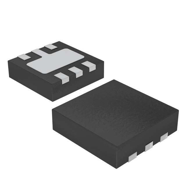
| 供应商器件封装 | 6-DFN-EP(2x2) |
| 其它名称 | AP133-SNG-7DICT |
| 包装 | 剪切带 (CT) |
| 安装类型 | 表面贴装 |
| 封装/外壳 | 6-UDFN 裸露焊盘 |
| 工作温度 | -40°C ~ 85°C |
| 标准包装 | 1 |
| 电压-跌落(典型值) | 0.35V @ 300mA |
| 电压-输入 | 2 V ~ 6 V |
| 电压-输出 | 1 V ~ 5 V |
| 电流-输出 | 300mA |
| 电流-限制(最小值) | 400mA |
| 稳压器拓扑 | 正,可调式 |
| 稳压器数 | 1 |


- 商务部:美国ITC正式对集成电路等产品启动337调查
- 曝三星4nm工艺存在良率问题 高通将骁龙8 Gen1或转产台积电
- 太阳诱电将投资9.5亿元在常州建新厂生产MLCC 预计2023年完工
- 英特尔发布欧洲新工厂建设计划 深化IDM 2.0 战略
- 台积电先进制程称霸业界 有大客户加持明年业绩稳了
- 达到5530亿美元!SIA预计今年全球半导体销售额将创下新高
- 英特尔拟将自动驾驶子公司Mobileye上市 估值或超500亿美元
- 三星加码芯片和SET,合并消费电子和移动部门,撤换高东真等 CEO
- 三星电子宣布重大人事变动 还合并消费电子和移动部门
- 海关总署:前11个月进口集成电路产品价值2.52万亿元 增长14.8%


PDF Datasheet 数据手册内容提取
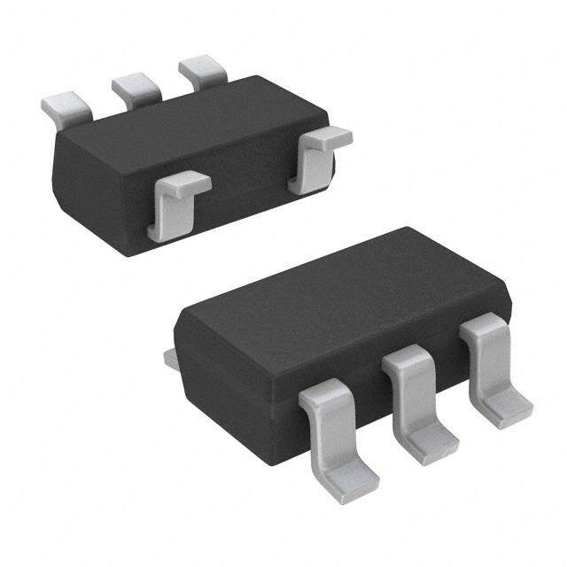
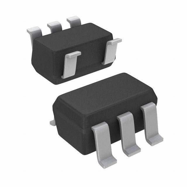
NOT RECOMMENDED FOR NEW DESIGN USE AP7330 or AP7343 AP133 Green 300mA, LOW QUIESCENT CURRENT, FAST TRANSIENT LOW DROPOUT LINEAR REGULATOR Description Pin Assignments The AP133 is a 300mA, adjustable output voltage, low dropout linear regulator. The device includes pass element, error amplifier, band- gap, current limit and thermal shutdown circuitry. The device is turned on when EN pin is set to logic high level. (Top View) The characteristics of low dropout voltage and less quiescent current make it good for low power applications, for example, battery IN 1 5 OUT powered devices. The typical quiescent current is approximately 40μA from zero to maximum load. GND 2 Built-in current-limit and thermal-shutdown functions prevent IC from damage in fault conditions. EN 3 4 ADJ The AP133 is available in SOT25 and DFN2020-6 packages. SOT25 Features 300mA Low Dropout Regulator with EN (Top View) Very Low IQ: 40µA Wide Input Voltage Range: 2V to 6V Adjustable Output: 1V to 5V EN 1 6 ADJ High PSRR: 65dB at 1kHz Ultra-fast Start-Up Time: 25µs GND 2 5 NC Stable with Low ESR, 1µF Ceramic Output Capacitor Excellent Load/Line Transient Response Low Dropout: 350mV at 300mA IN 3 4 OUT Current Limit Protection Short Circuit Protection Thermal Shutdown Protection DFN2020-6 Ambient Temperature Range: -40ºC to +85°C SOT25 and DFN2020-6: Available in “Green” Molding Applications Compound (No Br, Sb) Lead-Free Finish; RoHS Compliant (Notes 1 & 2) Cellular Phones Halogen and Antimony Free. “Green” Device (Note 3) Smart Phones, PDAs MP3/MP4 Bluetooth Head Set Low Power Application Notes: 1. EU Directive 2002/95/EC (RoHS), 2011/65/EU (RoHS 2) & 2015/863/EU (RoHS 3) compliant. All applicable RoHS exemptions applied. 2. See http://www.diodes.com/quality/lead_free/ for more information about Diodes Incorporated’s definitions of Halogen- and Antimony-free, "Green" and Lead-free. 3. Halogen- and Antimony-free "Green” products are defined as those which contain <900ppm bromine, <900ppm chlorine (<1500ppm total Br + Cl) and <1000ppm antimony compounds. AP133 1 of 16 June 2018 Document number: DS31122 Rev. 7 - 3 www.diodes.com © Diodes Incorporated
NOT RECOMMENDED FOR NEW DESIGN AP133 USE AP7330 or AP7343 Typical Applications Circuit V V IN OUT IN OUT AP133 R1 1mF 1mF Enable EN ADJ GND R2 R V V 1 1 OUT REF R 2 Pin Descriptions Package Name Pin Number Function SOT25 DFN2020-6 IN 1 3 Voltage input pin. Bypass to ground through at least 0.1µF capacitor GND 2 2 Ground EN 3 1 Enable input, active high ADJ 4 6 Output feedback pin NC - 5 No connection OUT 5 4 Voltage output pin. Bypass to ground through 1µF ceramic capacitor AP133 2 of 16 June 2018 Document number: DS31122 Rev. 7 - 3 www.diodes.com © Diodes Incorporated
NOT RECOMMENDED FOR NEW DESIGN AP133 USE AP7330 or AP7343 Functional Block Diagram IN OUT Current Limit Gate EN and Thermal Driver Shutdown FB 0.8V GND Absolute Maximum Ratings (@TA = +25°C, unless otherwise specified.) Symbol Parameter Ratings Unit VIN Input Voltage 7 V - OUT, ADJ, EN Voltage VIN + 0.3 V - Continuous Load Current Internal Limited - TOP Operating Junction Temperature Range -40 to +125 °C TST Storage Temperature Range -65 to +150 °C SOT25 740 mW PD Power Dissipation (Note 4) DFN2020-6 900 mW TJ Maximum Junction Temperature +150 °C Recommended Operating Conditions (@TA = +25°C, unless otherwise specified.) Symbol Parameter Min Max Unit VIN Input voltage (Note 5) 2 6 V IOUT Output Current 0 300 mA TA Operating Ambient Temperature -40 +85 °C Notes: 4. Ratings apply to ambient temperature at +25°C. 5. At VIN< 2.2V and TA< -20°C, the output current capability may be reduced. AP133 3 of 16 June 2018 Document number: DS31122 Rev. 7 - 3 www.diodes.com © Diodes Incorporated
NOT RECOMMENDED FOR NEW DESIGN AP133 USE AP7330 or AP7343 Electrical Characteristics (@TA = +25°C, VIN = VOUT +1V, CIN = 1mF, COUT = 1mF, VEN = 2V, unless otherwise specified.) Symbol Parameter Test Conditions Min Typ. Max Unit IQ Input Quiescent Current IOUT = 0~300mA - 40 60 mA ISHDN Input Shutdown Current VEN = 0V, IOUT = 0 - - 1 mA ILEAK Input Leakage Current VEN = 0V, OUT grounded - - 1 mA VDropout Dropout Voltage VOUT 1.5V, IOUT = 300mA - 350 450 mV VREF ADJ reference voltage IOUT= 0 - 0.8 - V IADJ ADJ leakage - - - 1 mA VOUT Output Voltage Accuracy - -2 - 2 % VOUT Line Regulation VIN = VOUT +1V to 5.5V, - 0.05 - %/V /VIN/V IOUT = 1mA VOUT Load Regulation IOUT from 1mA to 300mA -1 - 1 % /VOUT tST Start-up Time VIOEUNT == 03V0 0tom 2A. 0V, - 25 - ms PSRR PSRR 1kHz, IOUT = 0mA - 65 - dB ISHORT Short-circuit Current VIN = 5.0V, VOUT < 0.2V - 120 - mA ILIMIT Current limit VOUT = 3V, ROUT = 3Ω 400 600 - mA VIL EN Input Logic Low Voltage - - - 0.4 V VIH EN Input Logic High Voltage - 1.4 - - V IEN EN Input leakage VEN = 0V or 5.5V -1 - 1 uA TSHDN Thermal shutdown threshold - - +145 - °C THYS Thermal shutdown hysteresis - - +20 - °C Thermal Resistance SOT25 - 176 - θJA Junction-to-Ambient DFN2020-6 Device mounted on FR-4 substrate, - 142 - °C/W 2oz copper, with minimum Thermal Resistance SOT25 - 41 - θJC Junction-to-Case DFN2020-6 recommended pad layout. - 36 - °C/W AP133 4 of 16 June 2018 Document number: DS31122 Rev. 7 - 3 www.diodes.com © Diodes Incorporated
NOT RECOMMENDED FOR NEW DESIGN AP133 USE AP7330 or AP7343 Typical Performance Characteristics Output Voltage vs. Temperature Output Voltage vs. Temperature 3.3100 1.8200 VIN=5V, Vout=3.3V VIN=3.3V, Vout=1.8V ge (V)3.3050 e (V)1.8150 a g put Volt3.3000 ut Volta1.8100 Out utp 3.2950 O1.8050 3.2900 1.8000 -50.0 -25.0 0.0 25.0 50.0 75.0 100.0 125.0 -50.0 -25.0 0.0 25.0 50.0 75.0 100.0 125.0 Temperature (°C) Temperature (°C) Output Voltage vs. Input Voltage Quiescent Current vs. Input Voltage 2.0 60 VOUT=1.2V 1.8 A) IOUT=0mA m 55 ge (V)111...246 urrent ( 50 IOUT=300mA a C put Volt001...680 escent 4405 Out0.4 IOUT=0mA Qui 35 0.2 IOUT=150mA 0.0 30 0.0 1.0 2.0 3.0 4.0 5.0 6.0 2.0 3.0 4.0 5.0 6.0 Input Voltage (V) Input Voltage (V) Quiescent Current vs. I Quiescent Current vs. Temperature OUT VOUT=2.8V 60.00 50 Vin=3.3V A)m 55.00 Vin=5V A) ent ( 50.00 nt (m 45 Curr urre ent 45.00 nt C 40 esc 40.00 sce Qui 35.00 uie 35 VOUT=1.2V VIN=3.3V Q VOUT=3.3V VIN=5.0V 30.00 30 0.00 50.00 100.00 150.00 200.00 250.00 300.00 -50.0 -25.0 0.0 25.0 50.0 75.0 100.0 125.0 IOUT(mA) Temperature (°C) AP133 5 of 16 June 2018 Document number: DS31122 Rev. 7 - 3 www.diodes.com © Diodes Incorporated
NOT RECOMMENDED FOR NEW DESIGN AP133 USE AP7330 or AP7343 Typical Performance Characteristics Dropout Voltage vs. I ADJ Pin Voltage vs. Input Voltage OUT V =3.3V OUT 0.8020 450 400 V) 0.8015 mV)350 ge ( 0.8010 e (300 a g J Pin Volt 00..88000005 pout Volta122505000 D o100 25°C A 0.7995 Dr 50 90°C -45°C 0 0.7990 0.0 50.0 100.0 150.0 200.0 250.0 300.0 2.0 3.0 4.0 5.0 6.0 Input Voltage (V) I (mA) OUT Current Limit Protection Current Limit vs. Temperature 800 Vin=3.3V, Vout=1.2V A)750 Vin=5.0V, Vout=3.3V m mit (700 Li650 nt e urr600 C 550 500 -50 -30 -10 10 30 50 70 90 Temperature (°C) Time (50ms/div) Short Circuit Protection Short Circuit Protection Time (1ms/div) Time (2ms/div) AP133 6 of 16 June 2018 Document number: DS31122 Rev. 7 - 3 www.diodes.com © Diodes Incorporated
NOT RECOMMENDED FOR NEW DESIGN AP133 USE AP7330 or AP7343 Typical Performance Characteristics Short Circuit Current vs. Input Voltage Short Circuit Current vs. Temperature 150 Vin=3.3V, Vout=1.2V A) 150 mA) 140 Vin=3.3V, Vout=1.8V nt (m 113400 ent ( 130 Vin=5.0V, Vout=3.3V urre 120 Curr 120 ort Circuit C 1189010000 hort Circuit 11901000 h S S 70 80 2.0 3.0 4.0 5.0 6.0 -50 -30 -10 10 30 50 70 90 Temperature (°C) Input Voltage (V) Thermal Shutdown Protection PSRR -20.00 -30.00 -40.00 B) R (d-50.00 R-60.00 S P -70.00 -80.00 -90.00 100 1000 10000 100000 Frequency (Hz) Time (20ms/div) Line Transient Response Line Transient Response Time (20ms/div) Time (20ms/div) AP133 7 of 16 June 2018 Document number: DS31122 Rev. 7 - 3 www.diodes.com © Diodes Incorporated
NOT RECOMMENDED FOR NEW DESIGN AP133 USE AP7330 or AP7343 Typical Performance Characteristics Line Transient Response Line Transient Response Time (20ms/div) Time (20ms/div) Load Transient Response Load Transient Response Time (100ms/div) Time (100ms/div) Load Transient Response Load Transient Response Time (20ms/div) Time (100ms/div) AP133 8 of 16 June 2018 Document number: DS31122 Rev. 7 - 3 www.diodes.com © Diodes Incorporated
NOT RECOMMENDED FOR NEW DESIGN AP133 USE AP7330 or AP7343 Typical Performance Characteristics Start-up Time Start-up Time EN=VIN=5V EN=VIN=5V CIN=1mF CIN=1mF COUT=1mF COUT=1mF Time (5ms/div) Time (5ms/div) Start-up Time Start-up Time EN=VIN=3.3V EN=VIN=3.3V CIN=1mF CIN=1mF COUT=1mF COUT=1mF Time (5ms/div) Time (5ms/div) AP133 9 of 16 June 2018 Document number: DS31122 Rev. 7 - 3 www.diodes.com © Diodes Incorporated
NOT RECOMMENDED FOR NEW DESIGN AP133 USE AP7330 or AP7343 Application Note Input Capacitor A1mF ceramic capacitor is recommended to connect between VIN and GND pins to decouple input power supply glitch and noise. The amount of the capacitance may be increased without limit. This input capacitor must be located as close as possible to the device to assure input stability and less noise. For PCB layout, a wide copper trace is required for both VIN and GND. A lower ESR capacitor allows the use of less capacitance, while higher ESR type requires more capacitance. Output Capacitor The output capacitor is required to stabilize and help transient response for LDO. The AP133 is stable with very small ceramic output capacitors. The recommended capacitance is from 1mF to 4.7mF, Equivalent Series Resistance (ESR) is from 10m to 100m, and temperature characteristic is X7R or X5R. Higher capacitance values help to improve load/line transient response. The output capacitance may be increased to keep low undershoot/overshoot. Place output capacitor as close as possible to OUT and GND pins, and keep the leads as short as possible. Adjustable Operation The AP133 provides output voltage from 1.0V to 5.0V through external resistor divider as shown below. VIN AP133 VOUT IN OUT CIN R1 COUT Enable EN ADJ GN D R2 The output voltage is calculated by: R VOUT VREF1 R1 2 Where VREF=0.8V (the internal reference voltage) Rearranging the equation will give the following that is used for adjusting the output to a particular voltage: V R R OUT 1 1 2V REF To maintain the stability of the internal reference voltage, R2 needs to be kept smaller than 250k. No Load Stability Other than external resistor divider, no minimum load is required to keep the device stable. The device will remain stable and regulated in no load condition. ON/OFF Input Operation The AP133 is turned on by setting the EN pin high, and is turned off by pulling it low. If this feature is not used, the EN pin should be tied to IN pin to keep the regulator output on at all time. To ensure proper operation, the signal source used to drive the EN pin must be able to swing above and below the specified turn-on/off voltage thresholds listed in the Electrical Characteristics section under VIL and VIH. Current Limit Protection When output current at OUT pin is higher than current limit threshold, the current limit protection will be triggered and clamp the output current to approximately 600mA to prevent over-current and to protect the regulator from damage due to overheating. Short Circuit Protection When OUT pin is short-circuit to GND or OUT pin voltage is less than 200mV, short circuit protection will be triggered and clamp the output current to approximately 120mA. This feature protects the regulator from over-current and damage due to overheating. Thermal Shutdown Protection Thermal protection disables the output when the junction temperature rises to approximately +145°C, allowing the device to cool down. When the junction temperature reduces to approximately +125°C the output circuitry is enabled again. Depending on power dissipation, thermal resistance, and ambient temperature, the thermal protection circuit may cycle on and off. This cycling limits the heat dissipation of the regulator, protecting it from damage due to overheating. AP133 10 of 16 June 2018 Document number: DS31122 Rev. 7 - 3 www.diodes.com © Diodes Incorporated
NOT RECOMMENDED FOR NEW DESIGN AP133 USE AP7330 or AP7343 Application Note (Cont.) Ultra Fast Start-up After enabled, the AP133 is able to provide full power in as little as tens of microseconds, typically 25µs, without sacrificing low ground current. This feature will help load circuitry move in and out of standby mode in real time, eventually extend battery life for mobile phones and other portable devices. Fast Transient Response Fast transient response LDOs can also extend battery life. TDMA-based cell phone protocols such as Global System for Mobile Communications (GSM) have a transmit/receive duty factor of only 12.5 percent, enabling power savings by putting much of the baseband circuitry into standby mode in between transmit cycles. In baseband circuits, the load often transitions virtually instantaneously from 100µA to 100mA. To meet this load requirement, the LDO must react very quickly without a large voltage drop or overshoot — a requirement that cannot be met with conventional, general-purpose LDOs. The AP133’s fast transient response from 0 to 300mA provides stable voltage supply for fast DSP and GSM chipset with fast changing load. Small Overshoot and Undershoot The AP133 has small and controlled overshoot and undershoot in load and line transitions. This helps to protect supplied circuit from damage and operation error caused by glitches. This feature also permits the usage of small value output decoupling capacitor with AP133. Low Quiescent Current Cellular phone baseband internal digital circuits typically operate from 1.8V to 2.6V. When the Li+ battery voltage falls to 3.2 to 3.3V, most phones shut off, giving at least 500-600mV of headroom for the baseband digital LDO, so dropout is not critical. Output noise and the PSRR are not critical specs for the digital circuits. Nonetheless, this supply requires low quiescent current at light loads because this LDO stays on at all times. Figure below shows how the digital supply current of a representative GSM chipset core varies as a function of time. In the standby mode, the microprocessor consumes only around 200µA. Since the phone stays in standby for the longest percentage of time, using a 40µA quiescent current LDO, instead of 140µA, saves 100µA and extends the standby time by 340µA/240µA, or 1.417 times. The baseband internal analog circuit is typically 2.4V-3.0V, and it requires 200-600mV dropout. This LDO is on all the time, so it requires low quiescent current as well. The cellular phone real-time clock LDO needs a very low quiescent current, since this LDO is on all the time even though the handset is powered off. The AP133, consuming only around 40µA for all input range and output loading, provides great power saving in portable and low power applications. Wide Output Range The AP133, with a wide output range of 1.0V to 5.0V, provides a versatile LDO solution for many portable applications. High PSRR The RF circuit consists of receive and transmit sections, which typically require 2.6V-3.0V supply voltage. The RF circuits such as LNA (low-noise amplifier), up/down-converter, mixer, PLL, VCO, and IF stage, require low noise and high PSRR LDOs. The temperature-compensated crystal oscillator circuit requires very high PSRR at RF power amplifier burst frequency. For instance, minimum 65dB PSRR at 217Hz is recommended for the GSM handsets. In order to provide good audio quality, the audio power supply for hand-free, game, MP3, and multimedia applications in cellular phones, require low-noise and high PSRR at audio frequency range (20Hz to 20kHz). The AP133, with PSRR of 70dB at 1kHz in best case, is suitable for some of these applications that require high PSRR. AP133 11 of 16 June 2018 Document number: DS31122 Rev. 7 - 3 www.diodes.com © Diodes Incorporated
NOT RECOMMENDED FOR NEW DESIGN AP133 USE AP7330 or AP7343 Ordering Information AP 133 - XX G - 7 Package Green Packing W : SOT25 G : Green 7 : Tape & Reel SN : DFN2020-6 Packaging 7” Tape and Reel Device Package Code (Note 6) Quantity Part Number Suffix AP133-WG-7 W SOT25 3000/Tape & Reel -7 AP133-SNG-7 SN DFN2020-6 3000/Tape & Reel -7 Note: 6. Pad layout as shown on Diodes Incorporated’s suggested pad layout document, which can be found on our website at http://www.diodes.com/package-outlines.html. AP133 12 of 16 June 2018 Document number: DS31122 Rev. 7 - 3 www.diodes.com © Diodes Incorporated
NOT RECOMMENDED FOR NEW DESIGN AP133 USE AP7330 or AP7343 Marking Information (1) SOT25 ( Top View ) 5 4 7 XX : Identification code Y : Year 0~9 XX Y W X W : Week : A~Z : 1~26 week; a~z : 27~52 week; z represents 52 and 53 week 1 2 3 X : A~Z : Green Part Number Package Identification Code AP133-WG-7 SOT25 NB (2) DFN2020-6 ( Top View ) XX : Identification Code X X Y : Year : 0~9 W : Week : A~Z : 1~26 week; YWX a~z : 27~52 week; z represents 52 and 53 week X : A~Z : Green Part Number Package Identification Code AP133-SNG-7 DFN2020-6 NB AP133 13 of 16 June 2018 Document number: DS31122 Rev. 7 - 3 www.diodes.com © Diodes Incorporated
NOT RECOMMENDED FOR NEW DESIGN AP133 USE AP7330 or AP7343 Package Outline Dimensions (All dimensions in mm.) (1) Package Type: SOT25 (2) Package Type: DFN2020-6 3 n. 6 o 0. m 7/ 43 0.5 Marking 0. 0.05 C (Active area depth) x. a m 0.08 C 5 Seating plane 1 0. C 5 C 0 5 0/0. 0.1 2x 1.95/2.075 A B 1.45/1.65 0 1.95/2.075 0.76/0.96 0.30/0.4 R0.1 2x- 0.15 C 0.65nom. 0.2/0.3 0.05M C A B Pin#1 ID Bottom View AP133 14 of 16 June 2018 Document number: DS31122 Rev. 7 - 3 www.diodes.com © Diodes Incorporated
NOT RECOMMENDED FOR NEW DESIGN AP133 USE AP7330 or AP7343 Taping Orientation (Note 7) Note: 7. The taping orientation of the other package type can be found on our website at http://www.diodes.com/datasheets/ap02007.pdf. AP133 15 of 16 June 2018 Document number: DS31122 Rev. 7 - 3 www.diodes.com © Diodes Incorporated
NOT RECOMMENDED FOR NEW DESIGN AP133 USE AP7330 or AP7343 IMPORTANT NOTICE DIODES INCORPORATED MAKES NO WARRANTY OF ANY KIND, EXPRESS OR IMPLIED, WITH REGARDS TO THIS DOCUMENT, INCLUDING, BUT NOT LIMITED TO, THE IMPLIED WARRANTIES OF MERCHANTABILITY AND FITNESS FOR A PARTICULAR PURPOSE (AND THEIR EQUIVALENTS UNDER THE LAWS OF ANY JURISDICTION). Diodes Incorporated and its subsidiaries reserve the right to make modifications, enhancements, improvements, corrections or other changes without further notice to this document and any product described herein. Diodes Incorporated does not assume any liability arising out of the application or use of this document or any product described herein; neither does Diodes Incorporated convey any license under its patent or trademark rights, nor the rights of others. Any Customer or user of this document or products described herein in such applications shall assume all risks of such use and will agree to hold Diodes Incorporated and all the companies whose products are represented on Diodes Incorporated website, harmless against all damages. Diodes Incorporated does not warrant or accept any liability whatsoever in respect of any products purchased through unauthorized sales channel. Should Customers purchase or use Diodes Incorporated products for any unintended or unauthorized application, Customers shall indemnify and hold Diodes Incorporated and its representatives harmless against all claims, damages, expenses, and attorney fees arising out of, directly or indirectly, any claim of personal injury or death associated with such unintended or unauthorized application. Products described herein may be covered by one or more United States, international or foreign patents pending. Product names and markings noted herein may also be covered by one or more United States, international or foreign trademarks. This document is written in English but may be translated into multiple languages for reference. Only the English version of this document is the final and determinative format released by Diodes Incorporated. LIFE SUPPORT Diodes Incorporated products are specifically not authorized for use as critical components in life support devices or systems without the express written approval of the Chief Executive Officer of Diodes Incorporated. As used herein: A. Life support devices or systems are devices or systems which: 1. are intended to implant into the body, or 2. support or sustain life and whose failure to perform when properly used in accordance with instructions for use provided in the labeling can be reasonably expected to result in significant injury to the user. B. A critical component is any component in a life support device or system whose failure to perform can be reasonably expected to cause the failure of the life support device or to affect its safety or effectiveness. Customers represent that they have all necessary expertise in the safety and regulatory ramifications of their life support devices or systems, and acknowledge and agree that they are solely responsible for all legal, regulatory and safety-related requirements concerning their products and any use of Diodes Incorporated products in such safety-critical, life support devices or systems, notwithstanding any devices- or systems-related information or support that may be provided by Diodes Incorporated. Further, Customers must fully indemnify Diodes Incorporated and its representatives against any damages arising out of the use of Diodes Incorporated products in such safety-critical, life support devices or systems. Copyright © 2018, Diodes Incorporated www.diodes.com AP133 16 of 16 June 2018 Document number: DS31122 Rev. 7 - 3 www.diodes.com © Diodes Incorporated