ICGOO在线商城 > 射频/IF 和 RFID > RFID,RF 接入,监控 IC > TRF7970ARHBT
 Datasheet下载
- 型号: TRF7970ARHBT
- 制造商: Texas Instruments
- 库位|库存: xxxx|xxxx
- 要求:
| 数量阶梯 | 香港交货 | 国内含税 |
| +xxxx | $xxxx | ¥xxxx |
查看当月历史价格
查看今年历史价格
TRF7970ARHBT产品简介:
ICGOO电子元器件商城为您提供TRF7970ARHBT由Texas Instruments设计生产,在icgoo商城现货销售,并且可以通过原厂、代理商等渠道进行代购。 TRF7970ARHBT价格参考¥47.57-¥69.52。Texas InstrumentsTRF7970ARHBT封装/规格:RFID,RF 接入,监控 IC, RFID Reader/Transponder IC 13.56MHz ISO 14443, ISO 15693, ISO 18000-3 SPI 2.7V ~ 5.5V 32-VFQFN Exposed Pad。您可以下载TRF7970ARHBT参考资料、Datasheet数据手册功能说明书,资料中有TRF7970ARHBT 详细功能的应用电路图电压和使用方法及教程。
TRF7970ARHBT是德州仪器(Texas Instruments)推出的一款高度集成的多协议RFID和近场通信(NFC)收发器芯片,属于RFID、RF接入及监控IC类别。该芯片支持ISO/IEC 14443A/B、ISO/IEC 15693、Felica以及NFC Forum标准,适用于13.56MHz高频RFID系统。

其典型应用场景包括:智能门禁系统、公共交通票务系统(如公交卡、地铁卡读写器)、便携式支付终端(POS)、工业自动化设备的身份识别模块、医疗设备中的患者信息管理、电子产品中的安全认证与数据交换,以及智能家居中的NFC配对功能等。此外,TRF7970ARHBT还可用于资产跟踪、文档安全管理及消费类电子产品的无线配置连接。

该芯片采用小型化RHBT封装,具备低功耗特性,适合电池供电设备;同时支持SPI和I2C接口,便于与主控MCU连接,具备良好的系统集成性。其内置的模拟前端和自动防冲突功能提升了通信可靠性,广泛应用于需要非接触式数据传输和身份识别的中高端嵌入式系统中。
| 参数 | 数值 |
| 产品目录 | |
| 描述 | IC RFID/NFC AFE 13.56MHZ 32QFNRFID应答器 Fully Int 13.56MHz RFID/NFC Xcvr |
| DevelopmentKit | TRF7970AEVM |
| 产品分类 | RFID IC集成电路 - IC |
| 品牌 | Texas Instruments |
| 产品手册 | http://www.ti.com/litv/slos743k |
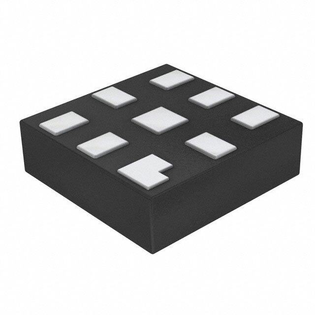
| 产品图片 |
|
| rohs | 符合RoHS无铅 / 符合限制有害物质指令(RoHS)规范要求 |
| 产品系列 | RF集成电路,RFID应答器,Texas Instruments TRF7970ARHBT- |
| 数据手册 | |
| 产品型号 | TRF7970ARHBT |
| RF类型 | NFC,FeliCa |
| 产品培训模块 | http://www.digikey.cn/PTM/IndividualPTM.page?site=cn&lang=zhs&ptm=30386http://www.digikey.cn/PTM/IndividualPTM.page?site=cn&lang=zhs&ptm=30389 |
| 产品种类 | RFID应答器 |
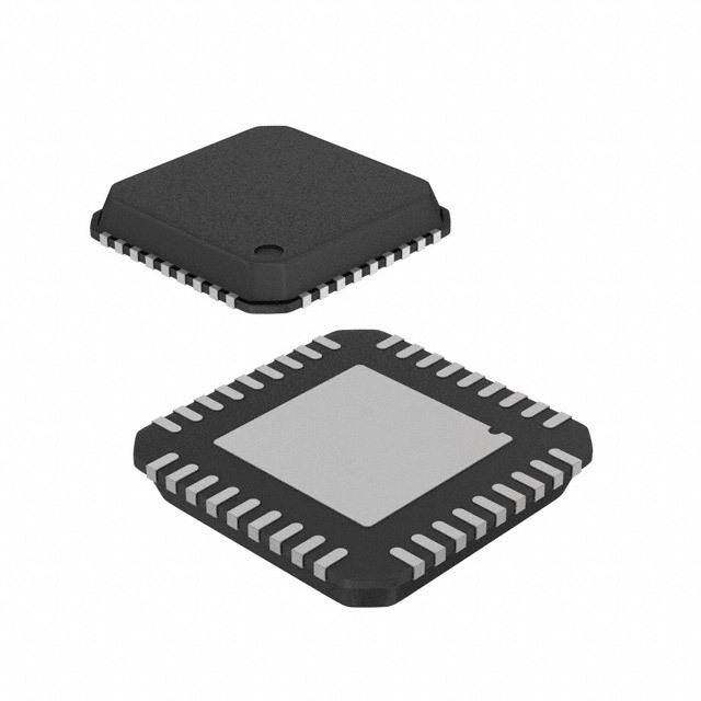
| 供应商器件封装 | 32-VQFN(5x5) |
| 其它名称 | 296-29476-1 |
| 制造商产品页 | http://www.ti.com/general/docs/suppproductinfo.tsp?distId=10&orderablePartNumber=TRF7970ARHBT |
| 包装 | 剪切带 (CT) |
| 参考设计库 | http://www.digikey.com/rdl/4294959884/4294959883/799 |
| 商标 | Texas Instruments |
| 安装风格 | SMD/SMT |
| 封装 | Reel |
| 封装/外壳 | 32-VFQFN 裸露焊盘 |
| 封装/箱体 | VQFN-32 |
| 工作温度范围 | - 40 C to + 110 C |
| 工厂包装数量 | 250 |
| 最大工作温度 | + 110 C |
| 最小工作温度 | - 40 C |
| 标准包装 | 1 |
| 特性 | ISO14443-A,ISO14443-B,ISO15693,ISO18000-3 |
| 系列 | TRF7970A |
| 配用 | /product-detail/zh/TRF7970AEVM/296-29475-ND/2745223 |
| 频率 | 13.56MHz |


- 商务部:美国ITC正式对集成电路等产品启动337调查
- 曝三星4nm工艺存在良率问题 高通将骁龙8 Gen1或转产台积电
- 太阳诱电将投资9.5亿元在常州建新厂生产MLCC 预计2023年完工
- 英特尔发布欧洲新工厂建设计划 深化IDM 2.0 战略
- 台积电先进制程称霸业界 有大客户加持明年业绩稳了
- 达到5530亿美元!SIA预计今年全球半导体销售额将创下新高
- 英特尔拟将自动驾驶子公司Mobileye上市 估值或超500亿美元
- 三星加码芯片和SET,合并消费电子和移动部门,撤换高东真等 CEO
- 三星电子宣布重大人事变动 还合并消费电子和移动部门
- 海关总署:前11个月进口集成电路产品价值2.52万亿元 增长14.8%


PDF Datasheet 数据手册内容提取
Product Order Technical Tools & Support & Reference Folder Now Documents Software Community Design TRF7970A SLOS743L–AUGUST2011–REVISEDMARCH2017 TRF7970A Multiprotocol Fully Integrated 13.56-MHz RFID and Near Field Communication (NFC) Transceiver IC 1 Device Overview 1.1 Features 1 • SupportsNearFieldCommunication(NFC) • ProgrammableOutputPower:+20dBm(100mW), StandardsNFCIP-1(ISO/IEC18092)andNFCIP‑2 +23dBm(200mW) (ISO/IEC21481) • ProgrammableI/OVoltageLevelsFrom1.8VDC • CompletelyIntegratedProtocolHandlingfor to5.5VDC ISO/IEC15693,ISO/IEC18000-3,ISO/IEC14443 • ProgrammableSystemClockFrequencyOutput AandB,andFeliCa™ (RF,RF/2,RF/4)from13.56-MHzor27.12-MHz • IntegratedEncoders,Decoders,andDataFraming CrystalorOscillator forNFCInitiator,ActiveandPassiveTarget • IntegratedVoltageRegulatorOutputforOther OperationforAllThreeBitRates(106kbps, SystemComponents(MCU,Peripherals, 212kbps,424kbps),andCardEmulation Indicators),20mA(Max) • RFFieldDetectorWithProgrammableWake-up • ProgrammableModulationDepth LevelsforNFCPassiveTransponderEmulation • DualReceiverArchitectureWithRSSIfor Operation Eliminationof"ReadHoles"andAdjacentReader • RFFieldDetectorforNFCPhysicalCollision SystemorAmbientIn-BandNoiseDetection Avoidance • ProgrammablePowerModesforUltraLow-Power • IntegratedStateMachineforISO/IEC14443A SystemDesign(PowerDown<1µA) Anticollision(BrokenBytes)Operation • ParallelorSPIInterface(With127-ByteFIFO) (TransponderEmulationorNFCPassiveTarget) • TemperatureRange:–40°Cto110°C • InputVoltageRange:2.7VDCto5.5VDC • 32-PinQFNPackage(5mm× 5mm) 1.2 Applications • MobileDevices(Tablets,Handsets) • Short-RangeWirelessCommunicationTasks • SecurePairing(Bluetooth®,Wi-Fi®,OtherPaired (FirmwareUpdates) WirelessNetworks) • ProductIdentificationorAuthentication • PublicTransportorEventTicketing • MedicalEquipmentorConsumables • PassportorPayment(POS)ReaderSystems • AccessControl,DigitalDoorLocks • SharingofElectronicBusinessCards 1.3 Description The TRF7970A device is an integrated analog front end (AFE) and multiprotocol data-framing device for a 13.56-MHz NFC/RFIDsystemsupportingallthreeNFCoperationmodes – reader/writer,peer-to-peer,and card emulation according to ISO/IEC 14443 A and B, Sony FeliCa, ISO/IEC 15693, NFCIP-1 (ISO/IEC 18092), and NFCIP-2 (ISO/IEC 21481). Built-in programming options make the device suitable forawiderangeofapplicationsforNFC,proximity,andvicinityidentificationsystems. The device is configured by selecting the desired protocol in the control registers. Direct access to all controlregistersallowsfinetuningofvariousreaderparametersasneeded. The TRF7970A device supports data rates up to 848 kbps with all framing and synchronization tasks for the ISO protocols onboard. The TRF7970A device also supports reader and writer mode for NFC Forum tag types 1, 2, 3, 4, and 5. Other standards and even custom protocols can be implemented by using one of the direct modes the device offers. These direct modes let the user fully control the AFE and also gain access to the raw subcarrier data or the unframed, but already ISO-formatted, data and the associated (extracted)clocksignal. 1 An IMPORTANT NOTICE at the end of this data sheet addresses availability, warranty, changes, use in safety-critical applications, intellectualpropertymattersandotherimportantdisclaimers.PRODUCTIONDATA.
TRF7970A SLOS743L–AUGUST2011–REVISEDMARCH2017 www.ti.com The receiver system has a dual-input receiver architecture to maximize communication robustness. The receivers also include various automatic and manual gain control options. The received signal strength fromtransponders,ambientsources,orinternallevelsisavailableintheRSSIregister. A SPI or parallel interface can be used for the communication between the MCU and the TRF7970A device. When the built-in hardware encoders and decoders are used, transmit and receive functions use a 127-byte FIFO register. For direct transmit or receive functions, the encoders or decoders can be bypassedsotheMCUcanprocessthedatainrealtime. The TRF7970A device supports a wide supply voltage range of 2.7 V to 5.5 V and data communication levelsfrom1.8Vto5.5VfortheMCUI/Ointerface. The transmitter has selectable output power levels of 100 mW (+20 dBm) or 200 mW (+23 dBm) equivalent into a 50-Ω load when using a 5-V supply and supports OOK and ASK modulation with selectablemodulationdepth. The built-in programmable auxiliary voltage regulator delivers up to 20 mA to supply an MCU and additionalexternalcircuitswithinthereadersystem. Integrated RF field detector with programmable wake-up levels, eight selectable power modes, and ultra- lowpoweroperationenableeasydevelopmentofrobustandcost-efficientdesignsforlongbatterylife. Start evaluating the TRF7970A multiprotocol transceiver IC with the TRF7970AEVM, TRF7970ATB, or DLP-7970ABP. DeviceInformation PARTNUMBER PACKAGE BODYSIZE TRF7970ARHB VQFN(32) 5mm×5mm 2 DeviceOverview Copyright©2011–2017,TexasInstrumentsIncorporated SubmitDocumentationFeedback ProductFolderLinks:TRF7970A
TRF7970A www.ti.com SLOS743L–AUGUST2011–REVISEDMARCH2017 1.4 Functional Block Diagram Figure1-1showstheblockdiagram. VDD_I/O RX_IN1 MUX PAhmapsleituadned Gain (RASUSXI) Logic I/O_0 Detector State I/O_1 RF Level Control Detector Logic I/O_2 RX_IN2 RSSI (Control I/O_3 (External) Registersand Phaseand (RMSaSinI) CoLmogmica)nd Level II//OO__45 Amplitude Gain Sh Detector anFdilAteGrC Digitizer MCU ifter I/O_6 VDD_PA Interface I/O_7 ISO Protocol Decoder IRQ Handling SYS_CLK TX_OUT Transmitter Framing Bit 127-Byte Analog Front End Framing FIFO DATA_CLK VIN Serial Conversion VDD_A VSS_PA CRC and Parity BAND_GAP EN VSS_A EN2 Digital Control VDD_RF ASK/OOK State Machine MOD Voltage SupplyRegulator Systems VSS_RF (SupplyRegulatorsand ReferenceVoltages) VDD_X OSC_IN VSS Crystal or Oscillator OSC_OUT Timing System VSS_D Copyright © 2017,Texas Instruments Incorporated Figure1-1.BlockDiagram Copyright©2011–2017,TexasInstrumentsIncorporated DeviceOverview 3 SubmitDocumentationFeedback ProductFolderLinks:TRF7970A
TRF7970A SLOS743L–AUGUST2011–REVISEDMARCH2017 www.ti.com Table of Contents 1 DeviceOverview......................................... 1 6.8 Transmitter–DigitalSection........................ 30 1.1 Features.............................................. 1 6.9 Transmitter–ExternalPowerAmplifierand ................................. ........................................... Subcarrier Detector 31 1.2 Applications 1 ............ ............................................ 6.10 TRF7970AICCommunicationInterface 31 1.3 Description 1 ............................. ............................ 6.11 TRF7970AInitialization 49 1.4 FunctionalBlockDiagram 3 2 Revision History......................................... 5 6.12 SpecialDirectModeforImprovedMIFARE™ ......................................... Compatibility 50 3 DeviceCharacteristics.................................. 7 .......................................... 6.13 NFCModes 50 ..................................... 3.1 RelatedProducts 7 ............ 6.14 DirectCommandsfromMCUtoReader 52 4 TerminalConfigurationandFunctions.............. 8 ................................. 6.15 RegisterDescription 56 .......................................... 4.1 PinDiagram 8 7 Applications,Implementation,andLayout........ 76 ................................... 4.2 SignalDescriptions 8 7.1 TRF7970AReaderSystemUsingSPIWithSS 5 Specifications........................................... 10 Mode................................................ 76 5.1 AbsoluteMaximumRatings ........................ 10 7.2 Layout Considerations.............................. 77 5.2 ESDRatings........................................ 10 7.3 ImpedanceMatchingTX_Out(Pin5)to50Ω...... 77 5.3 RecommendedOperatingConditions............... 10 7.4 ReaderAntennaDesignGuidelines ................ 78 5.4 ElectricalCharacteristics............................ 11 8 DeviceandDocumentationSupport............... 79 5.5 ThermalResistanceCharacteristics................ 12 8.1 GettingStartedandNextSteps..................... 79 5.6 Switching Characteristics........................... 12 8.2 Device Nomenclature............................... 79 6 DetailedDescription................................... 13 8.3 ToolsandSoftware................................. 80 6.1 Overview............................................ 13 8.4 DocumentationSupport............................. 80 6.2 SystemBlockDiagram.............................. 16 8.5 CommunityResources.............................. 81 6.3 PowerSupplies...................................... 16 8.6 Trademarks.......................................... 81 6.4 Receiver–AnalogSection.......................... 22 8.7 ElectrostaticDischargeCaution..................... 81 6.5 Receiver–DigitalSection........................... 23 8.8 Glossary............................................. 81 ................................... 6.6 OscillatorSection 28 9 Mechanical,Packaging,andOrderable 6.7 Transmitter–AnalogSection....................... 29 Information.............................................. 82 4 TableofContents Copyright©2011–2017,TexasInstrumentsIncorporated SubmitDocumentationFeedback ProductFolderLinks:TRF7970A
TRF7970A www.ti.com SLOS743L–AUGUST2011–REVISEDMARCH2017 2 Revision History NOTE:Pagenumbersforpreviousrevisionsmaydifferfrompagenumbersinthecurrentversion. ChangesfromApril18,2014toMarch27,2017 Page • CorrectedthedesignationofISO/IECstandardsthroughoutdocument;forexample,changedISO14443to ISO/IEC14443........................................................................................................................ 1 • ChangedthecontentsofSection1.3,Description............................................................................... 1 • AddedSection3.1,RelatedProducts ............................................................................................. 7 • MovedT fromSection5.2toSection5.1,AbsoluteMaximumRatings.................................................. 10 STG • MovedSection5.2andchangedtitlefromHandlingRatingstoESDRatings.............................................. 10 • AddedV andV toSection5.4,ElectricalCharacteristics ................................................................ 11 OL OH • ChangedtheTYPvalueofthef parameterfrom8to4MHzinSection5.4,ElectricalCharacteristics ....... 11 D_CLKmax • Throughoutdocument,removedsupportforapplicationcontrolofAutomaticGainControl(AGC)andReceiver GainAdjust,becausethesefeaturesweredesignedfortestfunctionalityandnotforproductionuse.................. 13 • AddedNFCType5tagstosupportedlistinSection6.1.1,RFIDandNFCOperation–ReaderandWriter........... 13 • Removedtheparagraphthatstarted"Thedesiredsystemofoperation(bitrate)isachievedby..."from Section6.1.2,NFCDeviceOperation–Initiator................................................................................ 14 • Removedtheparagraphthatstarted"Thedesiredsystemofoperation(bitrate)isachievedby..."from Section6.1.3,NFCDeviceOperation–Target................................................................................. 14 • Throughoutdocument,changed"tag"emulationoremulatorto"card"emulationoremulator........................... 14 • Addedthesentencethatstarts"Forinteroperabilitypurposes,TIrecommends..."inthefirstbulletedlistitemin Section6.1.3,NFCDeviceOperation–Target................................................................................. 15 • ChangedPOLLINGtoSENSF_REQinthebulletedlistitemthatstarts"Ifthefirstcommandisa SENSF_REQ..."anddeletedthesentencethatstarted"ThePOLLINGresponseissentin..."inSection6.1.3, NFCDeviceOperation–Target................................................................................................... 15 • Updatedthebulletedlistitemthatstarts"IfthefirstcommandisATR_REQ..."inSection6.1.3,NFCDevice Operation–Target ................................................................................................................. 15 • Changed"codedasISO14443"to"SENSB_REQ"inthebulletedlistitemthatstarts"Ifthefirstcommandisa SENSB_REQ..."inSection6.1.3,NFCDeviceOperation–Target.......................................................... 15 • Changed"FeliCa"to"peer-to-peer"inSection6.1.3.1,ActiveTarget,andSection6.1.3.2,PassiveTarget........... 15 • Updatedtheparagraphthatstarts"ThetransmissionofaresponsemustoccurafterRFcollisionavoidance..."in Section6.1.3.1,ActiveTarget .................................................................................................... 15 • Updatedtheparagraphthatstarts"Thetransmitsysteminpassivetargetmode..."inSection6.1.3.2,Passive Target................................................................................................................................. 15 • UpdatedthedescriptioninSection6.1.3.3,CardEmulation.................................................................. 16 • Addedthesentencethatstarts"ForapplicationsinwhichtheTRF7970Amaybesubjected..."inthesecond paragraphofSection6.3,PowerSupplies....................................................................................... 16 • ChangedV toV inthelastsentencethatreads"TheV outputcurrentshouldnotexceed20mA."in DD_A DD_X DD_X theNOTEinAnalogSupplyRegulator:V ................................................................................... 17 DD_A • Removedtheparagraphthatstarted"TheRFpoweramplifierregulator..."fromDigitalSupplyRegulator:V .... 17 DD_X • Changed250mVto400mVin"...a"DeltaVoltage"of400mVbelowV ...".............................................. 17 IN • Addedtheparagraphthatstarts"AsV isincreased,thesystem..."inSection6.3.2,SupplyRegulator DD_RF Settings .............................................................................................................................. 19 • Removedtheparagraphsthatstarted"Themainreceiveralsohas..."and"Bydefault,theAGCwindow comparator..."fromSection6.4.2,ReceiverGainandFilterStages ........................................................ 22 • ChangedTable6-5tomatchTable6-37......................................................................................... 23 • UpdatedSection6.5,Receiver–DigitalSection,toclarifyandremoveduplicatecontent................................ 23 • UpdatedthedescriptioninSection6.5.1.2,ExternalRSSI.................................................................... 27 • Removed"EquivalentSeriesResistance"fromTable6-9,MinimumCrystalRecommendations........................ 29 • Removedmentionof3-wireSPIandreplaced"IRQ"with"SlaveSelect"inthefirstparagraphofSection6.10.1, GeneralIntroduction................................................................................................................ 31 • UpdatedthedescriptionofFIFOlevelinterruptsinSection6.10.1.4,FIFOOperation.................................... 35 • Added"butrecommended"to"ItisoptionalbutrecommendedtoreadtheFIFOStatusregister..."in Section6.10.3,ReceptionofAirInterfaceData................................................................................. 37 • ChangedthetitleofSection6.10.4,DataTransmissionFromMCUtoTRF7970A........................................ 38 • Removedthesentencethatstarted"Thechoiceofoneofthesemodesoveranother..."fromSection6.10.5, SerialInterfaceCommunication(SPI)............................................................................................ 38 • Updatedtheparagraphthatstarts"TIrecommendsresettingtheFIFOafterreceivingdata..."in Copyright©2011–2017,TexasInstrumentsIncorporated RevisionHistory 5 SubmitDocumentationFeedback ProductFolderLinks:TRF7970A
TRF7970A SLOS743L–AUGUST2011–REVISEDMARCH2017 www.ti.com Section6.10.5.1,SerialInterfaceModeWithSlaveSelect(SS).............................................................. 43 • AddedtheNOTEthatstarts"Anadditionaldirectmode..."inSection6.10.6,DirectMode............................... 44 • AddedSection6.11,TRF7970AInitialization ................................................................................... 49 • ChangedtheapplicationreportthatisreferencedinSection6.12,SpecialDirectModeforImprovedMIFARE™ Compatibility......................................................................................................................... 50 • ChangedPOLLINGtoSENSF_REQandupdateddescriptioninthelistitemthatstarts"Ifthefirstcommandisa SENSF_REQ..."..................................................................................................................... 51 • Updatedthedescriptioninthelistitemthatstarts"IfthefirstcommandisATR_REQ..."................................. 51 • CorrecteddescriptionofB1Irq_colinTable6-18,IRQStatusRegister(0x0C)forNFCandCardEmulation Operation:changedfrom"(asdefinedinregister0x01)"to"(asdefinedinregister0x10)" .............................. 52 • RemovedmentionofcollisionavoidancecommandsfromSection6.13.2,Initiator........................................ 52 • AddedandupdatedcommentsinTable6-19,AddressandCommandWordBitDistribution............................ 52 • Removedcommandcode0x15,CloseSlotSequence,fromTable6-19,AddressandCommandWordBit Distribution .......................................................................................................................... 52 • Addedthesentencethatstarts"ThiscommandshouldbesentafteraSoftwareInitializationcommand..."in Section6.14.1.1,Idle(0x00)....................................................................................................... 53 • ChangedthedescriptioninSection6.14.1.3,InitialRFCollisionAvoidance(0x04)....................................... 54 • ChangedthedescriptioninSection6.14.1.4,ResponseRFCollisionAvoidance(0x05)................................. 54 • ChangedthedescriptioninSection6.14.1.5,ResponseRFCollisionAvoidance(0x06,n=0)......................... 54 • Added"ThisisusedbytheISO/IEC15693protocol"toSection6.14.1.11,TransmitNextTimeSlot(0x14).......... 55 • CorrecteddescriptionofB1Irq_colinTable6-43,IRQStatusRegister(0x0C):changedfrom"(asdefinedin register0x01)"to"(asdefinedinregister0x10)" ............................................................................... 67 • ChangedthedescriptionofB5:B3inTable6-47from"...AuxiliaryRSSIrepresentsthesignallevelatRX_IN2"to "...AuxiliaryRSSIrepresentsthesignallevelatRX_IN1"...................................................................... 69 • RemovedformerSection7.1,TRF7970AReaderSystemUsingParallelMicrocontrollerInterface..................... 76 • ChangedFigure7-1,ApplicationSchematic–SPIWithSSModeMCUInterface ........................................ 76 • UpdatedthedescriptioninSection7.1.2,Schematic .......................................................................... 76 • AddedSection8.1,GettingStartedandNextSteps ........................................................................... 79 • AddedSection8.2,DeviceNomenclature....................................................................................... 79 • AddedSection8.3,ToolsandSoftware.......................................................................................... 80 • UpdatedSection8.4,DocumentationSupport.................................................................................. 80 6 RevisionHistory Copyright©2011–2017,TexasInstrumentsIncorporated SubmitDocumentationFeedback ProductFolderLinks:TRF7970A
TRF7970A www.ti.com SLOS743L–AUGUST2011–REVISEDMARCH2017 3 Device Characteristics Table3-1liststhesupportedmodesofoperationforthe TRF7970Adevice. Table3-1.SupportedModesofOperation P2PINITIATORORREADER/WRITER CARDEMULATION P2PTARGET BITRATE BITRATE BITRATE TECHNOLOGY TECHNOLOGY TECHNOLOGY (kbps) (kbps) (kbps) NFC-AandNFC-B 106,212,424, (ISO/IEC14443AandB) 848(1) NFC-A,NFC-B 106 NFC-A 106 NFC-F(JIS:X6319-4) 212,424 N/A N/A NFC-F 212,424 NFC-V(ISO/IEC15693) 6.7,26.7 N/A N/A N/A N/A (1) 848kbpsappliestoreader/writermodeonly. 3.1 Related Products Forinformationaboutotherdevicesinthisfamilyofproductsorrelatedproducts,seethefollowinglinks. ProductsforTIWirelessConnectivity Connect more with the industry’s broadest wireless connectivity portfolio. ProductsforNFC/RFID TI provides one of the industry’s most differentiated NFC and RFID product portfolios and is your solution to meet a broad range of NFC connectivity and RFID identificationneeds. CompanionProductsforTRF7970A Review products that are frequently purchased or used with this product. ReferenceDesignsforTRF7970A The TI Designs Reference Design Library is a robust reference design library that spans analog, embedded processor, and connectivity. Created by TI experts to help you jump start your system design, all TI Designs include schematic or block diagrams, BOMs, and design files to speed your time to market. Search and download designsat ti.com/tidesigns. Copyright©2011–2017,TexasInstrumentsIncorporated DeviceCharacteristics 7 SubmitDocumentationFeedback ProductFolderLinks:TRF7970A
TRF7970A SLOS743L–AUGUST2011–REVISEDMARCH2017 www.ti.com 4 Terminal Configuration and Functions 4.1 Pin Diagram Figure4-1showsthepinoutforthe32-pinRHBpackage. VDD_X OSC_IN OSC_OUT VSS_D EN SYS_CLK DATA_CLK EN2 32 31 30 29 28 27 26 25 VDD_A 1 24 I/O_7 VIN 2 23 I/O_6 VDD_RF 3 22 I/O_5 VDD_PA 4 21 I/O_4 Pad TX_OUT 5 20 I/O_3 VSS_PA 6 19 I/O_2 VSS_RX 7 18 I/O_1 RX_IN1 8 17 I/O_0 9 10 11 12 13 14 15 16 RX_IN2 VSS BG ASK/OO IRQ MOD VSS_A VDD_I/O K Figure4-1.32-PinRHBPackage(TopView) 4.2 Signal Descriptions Table4-1describesthesignals. Table4-1.TerminalFunctions TERMINAL TYPE (1) DESCRIPTION NAME NO. V 1 OUT Internalregulatedsupply(2.7Vto3.4V)foranalogcircuitry DD_A V 2 SUP Externalsupplyinputtochip(2.7Vto5.5V) IN V 3 OUT Internalregulatedsupply(2.7Vto5V),normallyconnectedtoV (pin4) DD_RF DD_PA V 4 INP SupplyforPA;normallyconnectedexternallytoV (pin3) DD_PA DD_RF TX_OUT 5 OUT RFoutput(selectableoutputpower,100mWor200mW,withV =5V) DD V 6 SUP NegativesupplyforPA;normallyconnectedtocircuitground SS_PA V 7 SUP NegativesupplyforRXinputs;normallyconnectedtocircuitground SS_RX RX_IN1 8 INP MainRXinput RX_IN2 9 INP AuxiliaryRXinput V 10 SUP Chipsubstrateground SS BAND_GAP 11 OUT Bandgapvoltage(V =1.6V);internalanalogvoltagereference BG SelectionbetweenASKandOOKmodulation(0=ASK,1=OOK)fordirectmode0or1. ASK/OOK 12 BID Canbeconfiguredasanoutputtoprovidethereceivedanalogsignaloutput. (1) SUP=Supply,INP=Input,BID=Bidirectional,OUT=Output 8 TerminalConfigurationandFunctions Copyright©2011–2017,TexasInstrumentsIncorporated SubmitDocumentationFeedback ProductFolderLinks:TRF7970A
TRF7970A www.ti.com SLOS743L–AUGUST2011–REVISEDMARCH2017 Table4-1.TerminalFunctions(continued) TERMINAL TYPE (1) DESCRIPTION NAME NO. IRQ 13 OUT Interruptrequest INP Externaldatamodulationinputfordirectmode0or1 MOD 14 OUT Subcarrierdigitaldataoutput(seeregisters0x1Aand0x1B) V 15 SUP Negativesupplyforinternalanalogcircuits;connectedtoGND SS_A V 16 INP SupplyforI/Ocommunications(1.8VtoV )levelshifter.V shouldbeneverexceeded. DD_I/O IN IN I/O_0 17 BID I/Opinforparallelcommunication I/O_1 18 BID I/Opinforparallelcommunication I/Opinforparallelcommunication I/O_2 19 BID TXenable(inspecialdirectmode) I/Opinforparallelcommunication I/O_3 20 BID TXdata(inspecialdirectmode) I/Opinforparallelcommunication I/O_4 21 BID SlaveselectsignalinSPImode I/Opinforparallelcommunication I/O_5 22 BID Dataclockoutputindirectmode1andspecialdirectmode I/Opinforparallelcommunication I/O_6 23 BID MISOforserialcommunication(SPI) Serialbitdataoutputindirectmode1orsubcarriersignalindirectmode0 I/Opinforparallelcommunication. I/O_7 24 BID MOSIforserialcommunication(SPI) Selectionofpowerdownmode.IfEN2isconnectedtoV ,thenV isactiveduringpower EN2 25 INP IN DD_X downmode2(forexample,tosupplytheMCU). DATA_CLK 26 INP DataclockinputforMCUcommunication(parallelandserial) IfEN=1(EN2=don'tcare)thesystemclockforMCUisconfigured.Dependingonthecrystal thatisused,optionsareasfollows(seeregister0x09): SYS_CLK 27 OUT 13.56-MHzcrystal:Off,3.39MHz,6.78MHz,or13.56MHz 27.12-MHzcrystal:Off,6.78MHz,13.56MHz,or27.12MHz IfEN=0andEN2=1,thensystemclockissetto60kHz EN 28 INP Chipenableinput(IfEN=0,thenchipisinsleeporpower-downmode). V 29 SUP Negativesupplyforinternaldigitalcircuits SS_D OSC_OUT 30 OUT Crystaloroscillatoroutput INP Crystaloroscillatorinput OSC_IN 31 OUT Crystaloscillatoroutput Internallyregulatedsupply(2.7Vto3.4V)fordigitalcircuitandexternaldevices(forexample, V 32 OUT DD_X anMCU) ThermalPad PAD SUP Chipsubstrateground Copyright©2011–2017,TexasInstrumentsIncorporated TerminalConfigurationandFunctions 9 SubmitDocumentationFeedback ProductFolderLinks:TRF7970A
TRF7970A SLOS743L–AUGUST2011–REVISEDMARCH2017 www.ti.com 5 Specifications 5.1 Absolute Maximum Ratings(1) (2) overoperatingfree-airtemperaturerange(unlessotherwisenoted) MIN MAX UNIT V Inputvoltagerange –0.3 6 V IN I MaximumcurrentV 150 mA IN IN Anycondition 140 °C T Maximumoperatingvirtualjunctiontemperature J Continuousoperation,long-termreliability(3) 125 °C T Storagetemperature –55 150 °C STG (1) StressesbeyondthoselistedunderAbsoluteMaximumRatingsmaycausepermanentdamagetothedevice.Thesearestressratings onlyandfunctionaloperationofthedeviceattheseoranyotherconditionsbeyondthoseindicatedunderRecommendedOperating Conditionsarenotimplied.Exposuretoabsolute-maximum-ratedconditionsforextendedperiodsmayaffectdevicereliability. (2) AllvoltagevaluesarewithrespecttosubstrategroundterminalV . SS (3) Themaximumjunctiontemperatureforcontinuousoperationislimitedbypackageconstraints.Operationabovethistemperaturemay resultinreducedreliabilityorlifetimeofthedevice. 5.2 ESD Ratings VALUE UNIT Human-bodymodel(HBM),perANSI/ESDA/JEDECJS-001,allpins(1) ±2000 V Charged-devicemodel(CDM),perJEDECspecificationJESD22-C101,all V(ESD) Electrostaticdischarge pins(2) ±500 V Machinemodel(MM) ±200 V (1) JEDECdocumentJEP155statesthat500-VHBMallowssafemanufacturingwithastandardESDcontrolprocess.Pinslistedas±2000 Vmayactuallyhavehigherperformance. (2) JEDECdocumentJEP157statesthat250-VCDMallowssafemanufacturingwithastandardESDcontrolprocess.Pinslistedas±500V mayactuallyhavehigherperformance. 5.3 Recommended Operating Conditions overoperatingfree-airtemperaturerange(unlessotherwisenoted) MIN TYP MAX UNIT V Operatinginputvoltage 2.7 5 5.5 V IN T Operatingambienttemperature –40 25 110 °C A T Operatingvirtualjunctiontemperature –40 25 125 °C J I/Olines,IRQ,SYS_CLK,DATA_CLK, 0.2× V Inputvoltage,logiclow V IL EN,EN2,ASK/OOK,MOD V DD_I/O I/Olines,IRQ,SYS_CLK,DATA_CLK, 0.8× V Inputvoltagethreshold,logichigh V IH EN,EN2,ASK/OOK,MOD V DD_I/O 10 Specifications Copyright©2011–2017,TexasInstrumentsIncorporated SubmitDocumentationFeedback ProductFolderLinks:TRF7970A
TRF7970A www.ti.com SLOS743L–AUGUST2011–REVISEDMARCH2017 5.4 Electrical Characteristics TYPoperatingconditionsareT =25°C,VIN=5V,full-powermode(unlessotherwisenoted) A MINandMAXoperatingconditionsareoverrecommendedrangesofsupplyvoltageandoperatingfree-airtemperature (unlessotherwisenoted) PARAMETER TESTCONDITIONS MIN TYP MAX UNIT 0.2× V Low-leveloutputvoltage V OL V DD_I/O 0.8× V High-leveloutputvoltage V OH V DD_I/O Allbuildingblocksdisabled,including I Supplycurrentinpowerdownmode1 supply-voltageregulators;measuredafter 0.5 5 µA PD1 500-mssettlingtime(EN=0,EN2=0) TheSYS_CLKgeneratorandV DD_X Supplycurrentinpowerdownmode2 remainactivetosupportexternalcircuitry; I 120 200 µA PD2 (sleepmode) measuredafter100-mssettlingtime (EN=0,EN2=1) Oscillatorrunning,supply-voltage I Supplycurrentinstand-bymode regulatorsinlow-consumptionmode 1.9 3.5 mA STBY (EN=1,EN2=x) Supplycurrentwithoutantennadriver Oscillator,regulators,RXandAGC I 10.5 14 mA ON1 current active,TXisoff Oscillator,regulators,RXandAGCand I Supplycurrent,TX(halfpower) 70 78 mA ON2 TXactive,P =100mW OUT Oscillator,regulators,RXandAGCand I Supplycurrent,TX(fullpower) 130 150 mA ON3 TXactive,P =200mW OUT V Power-on-resetvoltage InputvoltageatV 1.4 2 2.6 V POR IN V Bandgapvoltage(pin11) Internalanalogreferencevoltage 1.5 1.6 1.7 V BG Regulatedoutputvoltageforanalog V V =5V 3.1 3.4 3.8 V DD_A circuitry(pin1) IN V Regulatedsupplyforexternalcircuitry Outputvoltagepin32,V =5V 3.1 3.4 3.8 V DD_X IN I MaximumoutputcurrentofV Outputcurrentpin32,V =5V 20 mA VDD_Xmax DD_X IN Half-powermode,V =2.7Vto5.5V 8 12 R Antennadriveroutputresistance (1) IN Ω RFOUT Full-powermode,V =2.7Vto5.5V 4 6 IN R RX_IN1andRX_IN2inputresistance 4 10 20 kΩ RFIN MaximumRFinputvoltageatRX_IN1 V V shouldnotexceedV 3.5 V RF_INmax andRX_IN2 RF_INmax IN pp MinimumRFinputvoltageatRX_IN1 fSUBCARRIER=424kHz 1.4 2.5 VRF_INmin andRX_IN2(inputsensitivity)(2) f =848kHz 2.1 3 mVpp SUBCARRIER f SYS_CLKfrequency Inpowermode2,EN=0,EN2=1 25 60 120 kHz SYS_CLK f Carrierfrequency Definedbyexternalcrystal 13.56 MHz C Timeuntiloscillatorstablebitisset tCRYSTAL Crystalrun-intime (register0x0F)(3) 3 ms fD_CLKmax MaximumDATA_CLKfrequency(4) Dlineepse,nTdIsreocnocmampaecnidtisve2loMaHdzo(4n)theI/O 2 4 10 MHz R OutputresistanceI/O_0toI/O_7 500 800 Ω OUT R OutputresistanceR 200 400 Ω SYS_CLK SYS_CLK (1) Antennadriveroutputresistance (2) MeasuredwithsubcarriersignalatRX_IN1orRX_IN2andmeasuredthedigitaloutputatMODpinwithregister0x1Abit6=1. (3) Dependsonthecrystalparametersandcomponents (4) TIrecommendsaDATA_CLKspeedof2MHz.Higherdataclockdependsonthecapacitiveload.MaximumSPIclockspeedshouldnot exceed10MHz.Thisclockspeedisacceptableonlywhenexternalcapacitiveloadislessthan30pF.MISOdriverhasatypicaloutput resistanceof400Ω(12-nstimeconstantwhen30-pFloadused). Copyright©2011–2017,TexasInstrumentsIncorporated Specifications 11 SubmitDocumentationFeedback ProductFolderLinks:TRF7970A
TRF7970A SLOS743L–AUGUST2011–REVISEDMARCH2017 www.ti.com 5.5 Thermal Resistance Characteristics POWERRATING(2) PACKAGE θ θ (1) JC JA T ≤25°C T ≤85°C A A RHB(32pin) 31°C/W 36.4°C/W 2.7W 1.1W (1) ThisdatawastakenusingtheJEDECstandardhigh-KtestPCB. (2) Powerratingisdeterminedwithajunctiontemperatureof125°C.Thisisthetemperatureatwhichdistortionstartstoincrease substantially.ThermalmanagementofthefinalPCBshouldstrivetokeepthejunctiontemperatureatorbelow125°Cforbest performanceandlong-termreliability. 5.6 Switching Characteristics TYPoperatingconditionsareT =25°C,VIN=5V,full-powermode(unlessotherwisenoted) A MINandMAXoperatingconditionsareoverrecommendedrangesofsupplyvoltageandoperatingfree-airtemperature (unlessotherwisenoted) PARAMETER TESTCONDITIONS MIN TYP MAX UNIT DATA_CLKtimehighorlow,onehalfofDATA_CLKat Dependsoncapacitiveloadonthe tLO/HI 50%dutycycle I/Olines(1) 250 62.5 50 ns t Slaveselectleadtime,slaveselectlowtoclock 200 ns STE,LEAD t Slaveselectlagtime,lastclocktoslaveselecthigh 200 ns STE,LAG Slaveselectdisabletime,slaveselectrisingedgeto t 300 ns STE,DIS nextslaveselectfallingedge t MOSIinputdatasetuptime 15 ns SU,SI t MOSIinputdataholdtime 15 ns HD,SI t MISOinputdatasetuptime 15 ns SU,SO t MISOinputdataholdtime 15 ns HD,SO DATA_CLKedgetoMISOvalid, t MISOoutputdatavalidtime 30 50 75 ns VALID,SO C ≤30pF L (1) TIrecommendsaDATA_CLKspeedof2MHz.Higherdataclockdependsonthecapacitiveload.MaximumSPIclockspeedshouldnot exceed10MHz.Thisclockspeedisacceptableonlywhenexternalcapacitiveloadislessthan30pF.MISOdriverhasatypicaloutput resistanceof400Ω(12-nstimeconstantwhen30-pFloadused). 12 Specifications Copyright©2011–2017,TexasInstrumentsIncorporated SubmitDocumentationFeedback ProductFolderLinks:TRF7970A
TRF7970A www.ti.com SLOS743L–AUGUST2011–REVISEDMARCH2017 6 Detailed Description 6.1 Overview 6.1.1 RFID and NFC Operation – Reader and Writer The TRF7970A is a high-performance 13.56-MHz HF RFID and NFC transceiver IC composed of an integrated analog front end (AFE) and a built-in data framing engine for ISO/IEC 15693, ISO/IEC 14443 A and B, and FeliCa. This includes data rates up to 848 kbps for ISO/IEC 14443 with all framing and synchronization tasks on board (in default mode). The TRF7970A also supports NFC tag type 1, 2, 3, 4, and 5 operations. This architecture lets the customer build a complete cost-effective yet high-performance multiprotocol13.56-MHzRFID andNFCsystemtogetherwithalow-costmicrocontroller. Other standards and even custom protocols can be implemented by using either of the direct modes that the device offers. These direct modes (0 and 1) allow the user to fully control the analog front end (AFE) and also gain access to the raw subcarrier data or the unframed but already ISO formatted data and the associated(extracted)clocksignal. The receiver system has a dual input receiver architecture. The receivers also include various automatic and manual gain control options. The received input bandwidth can be selected to cover a broad range of inputsubcarriersignaloptions. The received signal strength from transponders, ambient sources, or internal levels is available through the RSSI register. The receiver output is selectable among a digitized subcarrier signal and any of the integrated subcarrier decoders. The selected subcarrier decoder delivers the data bit stream and the data clockasoutputs. The TRF7970A also includes a receiver framing engine. This receiver framing engine performs the CRC or parity check, removes the EOF and SOF settings, and organizes the data in bytes for ISO/IEC 14443 A and B, ISO/IEC 15693, and FeliCa protocols. Framed data is then accessible to the microcontroller (MCU) througha127-byteFIFOregister. V DD VDD_X VDD_I/O VDD TX_OUT Matching Parallel MCU TRF7970A RX_IN 1 or SPI (MSP430 orARM) RX_IN2 V V XIN SS IN Crystal 13.56 MHz Supply: 2.7 V to 5.5 V Figure6-1.ApplicationBlockDiagram A parallel or serial interface (SPI) can be used for the communication between the MCU and the TRF7970A reader. When the built-in hardware encoders and decoders are used, transmit and receive functions use a 127-byte FIFO register. For direct transmit or receive functions, the encoders and decoders can be bypassed so that the MCU can process the data in real time. The TRF7970A supports data communication voltage levels from 1.8 V to 5.5 V for the MCU I/O interface. The transmitter has selectable output-power levels of 100 mW (+20 dBm) or 200 mW (+23 dBm) equivalent into a 50-Ω load whenusinga5-Vsupply. Copyright©2011–2017,TexasInstrumentsIncorporated DetailedDescription 13 SubmitDocumentationFeedback ProductFolderLinks:TRF7970A
TRF7970A SLOS743L–AUGUST2011–REVISEDMARCH2017 www.ti.com ThetransmittersupportsOOKandASKmodulationwithselectablemodulationdepth.The TRF7970Aalso includes a data transmission engine that comprises low-level encoding for ISO/IEC 15693, ISO/IEC 14443 A and B, and FeliCa. Included with the transmit data coding is the automatic generation of Start Of Frame (SOF),EndOfFrame(EOF),CyclicRedundancyCheck(CRC),andparitybits. Several integrated voltage regulators ensure a proper power-supply noise rejection for the complete readersystem.Thebuilt-inprogrammableauxiliaryvoltageregulatorV (pin32),isabletodeliverupto DD_X 20mAtosupplyamicrocontrollerandadditionalexternalcircuitswithinthereadersystem. 6.1.2 NFC Device Operation – Initiator The transmitting system includes an RF level detector (programmable level) which is used for initial (or response) RF collision avoidance. The RF collision avoidance sequence is started by sending a direct command. If successful, the NFC initiator can send the data or commands, the MCU has loaded in the FIFO register. The coding of this data is done by hardware coders in ISO/IEC 14443 A and B, or FeliCa format. The coders also provide CRC and parity bits (if required) and automatically add preambles, SOF, EOF,andsynchronizationbytesasdefinedbyselectedprotocol. The receiver system offers the same analog features (AGC, AM or PM, bandwidth selection, and so on) as described previously in RFID and NFC reader and writer description. The system comprises integrated decoders for passive targets (ISO/IEC 14443 A or ISO/IEC 14443 B tag or FeliCa) or active targets (ISO/IEC 14443 A or ISO/IEC 14443 B reader or FeliCa). For all this options, the system also supports framing including CRC and parity check and removal of SOF, EOF, and synchronization bytes as specifiedbytheselectedprotocol. 6.1.3 NFC Device Operation – Target The activation of NFC target is done when a sufficient RF field level is detected on the antenna. The level neededforwake-upisselectableandisstoredinanonvolatileregister. When the activation occurs, the system performs automatic power-up and waits for the first command to be received. Based on this command, the system knows if it should operate as passive or active target and at what bit rate. After activation, the receiver system offers the same analog features (for example, AGC,AM/PM,andbandwidthselection)asinthecaseofanRFIDreader. When used as the NFC target, the chip is typically in a power down or standby mode. If EN2 = H, the chip keeps the supply system on. If EN2 = L and EN = L, the chip is in complete power down. To operate as NFC target or card emulator, the MCU must load a value different from zero (0) in the Target Detection Level register (B0-B2) to enable the RF measurement system (supplied by VEXT, so it can also operate during complete power down and consume only 3.5 µA). The RF measurement constantly monitors the RF signal on the antenna input. When the RF level on the antenna input exceeds the level defined in the inTargetDetectionLevelregister,thechipisautomaticallyactivated(ENisinternallyforcedhigh). When the voltage supply system and the oscillator are started and are stable, osc_ok goes high (B6 of RSSI Level and Oscillator Status register) and IRQ is sent with bit B2 = 1 of IRQ register (field change). Bit B7 NFC Target Protocol in register directly displays the status of RF level detection (running constantly also during normal operation). This informs the MCU that the chip should start operation as NFC TARGET device. When the first command from the INITIATOR is received, another IRQ sent with B6 (RX start) set in the IRQ register. The MCU must set EN = H (confirm the power up) in the time between the two IRQs, because the internal power-up ends after the second IRQ. The type and coding of the first initiator (or reader in the case of a card emulator) command defines the communication protocol type that the target must use. Therefore, the communication protocol type is available in the NFC Target Protocol register immediatelyafterreceivingthefirstcommand. 14 DetailedDescription Copyright©2011–2017,TexasInstrumentsIncorporated SubmitDocumentationFeedback ProductFolderLinks:TRF7970A
TRF7970A www.ti.com SLOS743L–AUGUST2011–REVISEDMARCH2017 BasedonthefirstcommandfromtheINITIATOR,thefollowingactionsaretaken: • If the first command is SENS_REQ or ALL_REQ, the TARGET must enter the SDD protocol for 106- kbps passive communication to begin; afterward, the baud rate can be changed to 212 kbps or 424 kbps, which is determined by the NFC initiator device. If bit B5 in the NFC Target Detection Level register is not set, the MCU handles the SDD and the command received is send to FIFO. For interoperability purposes, TI recommends allowing the MCU to handle the SDD process rather than use the TRF7970A Auto-SDD feature to ensure interoperability with other NFC devices. If the RF field is turned off (B7 in NFC Target Protocol register is low) at any time, the system sends an IRQ to the MCU with bit B2 (RF field change) in the IRQ register set high. This informs the MCU that the procedure was aborted and the system must be reset. The clock extractor is automatically activated in thismode. • If the command is SENS_REQ or ALL_REQ and the card emulation bit in ISO Control register is set, the system emulates an ISO/IEC 14443 A or ISO/IEC 14443 B tag. The procedure does not differ from the one previously described for the case of a passive target at 106 kbps. The clock extractor is automaticallyactivatedinthismode. • If the first command is a SENSF_REQ, the system becomes the TARGET in passive communication using212kbpsor424kbps.TheSDDisrelativelysimpleandishandledbytheMCUdirectly. • If the first command is ATR_REQ, the system operates as an active TARGET using the same communication speed and bit coding as used by the INITIATOR. Again, all of the replies are handled by the MCU. The MCU should handle the timing requirements for collision avoidance. This is done by usingexternalRSSItodetectexternalRFfieldsbeforeenablingRFontheTRF7970A. • If the first command is a SENSB_REQ request and the card emulation bit is set in the ISO Control register,thesystementersISO/IEC14443Bemulationmode.Theanticollisionmustbehandledbythe MCU,andthechipprovidesallphysicallevelcoding,decoding,andframingforthisprotocol. 6.1.3.1 ActiveTarget If the first command received by the RF interface defines the system as an active target, then the receiver selects the appropriate data decoders (ISO/IEC 14443 A or ISO/IEC 14443 B reader or peer-to-peer) and framing option. Only the raw (decoded) data is forwarded to the MCU through the FIFO. SOF, EOF, preamble,syncbytes,CRC,andparitybytesarecheckedbytheframeranddiscarded. The transmission of a response must occur after RF collision avoidance has been processed. The recommended method for RF collision avoidance is to use external RSSI to detect any external RF field. If successful, the NFC initiator can send the data that the MCU has loaded in the FIFO register. The coding ofthisdataisdonebyhardwarecoderseitherinISO/IEC14443Aformat(106-kbpssystem)orinpeer-to- peer format for (212-kbps and 424-kbps systems). The coders also provide CRC and parity bits (if required) and automatically add preambles, SOF, EOF, and synchronization bytes as defined by selected protocol. 6.1.3.2 PassiveTarget IfthefirstcommandreceivedbytheRFinterfacedefinesthesystemasapassivetarget,thenthereceiver selects the appropriate data decoders (ISO/IEC 14443 A or ISO/IEC 14443 B reader or peer-to-peer) and framing option. Again, only the raw (decoded) data is forwarded to the MCU through the FIFO; SOF, EOF, preamble, sync bytes, CRC, and parity bytes are checked by the framer and discarded. The receiver workssameasinthecaseofanactivetarget. The transmit system in passive target mode differs from active target and operates similar to the standard tag. There is no RF collision avoidance sequence, and encoders are used to code the data for ISO/IEC 14443 A or ISO/IEC 14443 B tag (at 106 kbps, to start) or peer-to-peer (at 212 kbps, to start) format. The coding system adds all of the SOF, EOF, CRC, parity bits, and synchronization bytes that are requiredbyprotocol.Theresponseistransmittedover-the-airwithamethodknownasloadmodulation. Copyright©2011–2017,TexasInstrumentsIncorporated DetailedDescription 15 SubmitDocumentationFeedback ProductFolderLinks:TRF7970A
TRF7970A SLOS743L–AUGUST2011–REVISEDMARCH2017 www.ti.com 6.1.3.3 CardEmulation The chip can enter this mode by setting appropriate option bits. The chip can emulate ISO/IEC 14443 A and B card types. For ISO/IEC 14443 A and B, the emulation supports 106-kbps data rate to start. For ISO/IEC 14443 A, the anticollision algorithm can be performed using an internal state machine, which relieves the MCU of any real-time tasks; however, this method can present interoperability challenges with other NFC devices due to timing requirements. To ensure best interoperability, TI recommends allowing the MCU to manage the anticollision process, instead. The unique ID required for anticollision is provided bytheMCUafterwakeupofthesystem. 6.2 System Block Diagram Figure6-2showsablockdiagramofthe TRF7970A. VDD_I/O RX_IN1 MUX PAhmapsleituadned Gain (RASUSXI) Logic I/O_0 Detector State I/O_1 RF Level Control Detector Logic I/O_2 RX_IN2 RSSI (Control I/O_3 (External) Registersand Phaseand (RMSaSinI) CoLmogmica)nd Level II//OO__45 Amplitude Gain Sh Detector anFdilAteGrC Digitizer MCU ifter I/O_6 VDD_PA Interface I/O_7 ISO Protocol Decoder IRQ Handling SYS_CLK TX_OUT Transmitter Framing Bit 127-Byte Analog Front End Framing FIFO DATA_CLK VIN Serial Conversion VDD_A VSS_PA CRC and Parity BAND_GAP EN VSS_A EN2 Digital Control VDD_RF ASK/OOK State Machine MOD Voltage SupplyRegulator Systems VSS_RF (SupplyRegulatorsand ReferenceVoltages) VDD_X OSC_IN VSS Crystal or Oscillator OSC_OUT Timing System VSS_D Copyright © 2017,Texas Instruments Incorporated Figure6-2.SystemBlockDiagram 6.3 Power Supplies The TRF7970A positive supply input V (pin 2) sources three internal regulators with output voltages IN V , V and V . All regulators use external bypass capacitors for supply noise filtering and must DD_RF DD_A DD_X be connected as indicated in reference schematics. These regulators provide a high power supply reject ratio(PSRR)asrequiredforRFIDreadersystems.AllregulatorsaresuppliedbyV (pin2). IN The regulators are not independent and have common control bits in register 0x0B for output voltage setting. The regulators can be configured to operate in either automatic or manual mode (register 0x0B, bit 7). The automatic regulator setting mode ensures an optimal compromise between PSRR and the highest possible supply voltage for RF output (to ensure maximum RF power output). The manual mode allows the user to manually configure the regulator settings. For applications in which the TRF7970A may besubjectedtoexternalnoise,manuallyreducingtheregulatorsettingscanimproveRFperformance. 16 DetailedDescription Copyright©2011–2017,TexasInstrumentsIncorporated SubmitDocumentationFeedback ProductFolderLinks:TRF7970A
TRF7970A www.ti.com SLOS743L–AUGUST2011–REVISEDMARCH2017 6.3.1 Supply Arrangements RegulatorSupplyInput:V IN The positive supply at V (pin 2) has an input voltage range of 2.7 V to 5.5 V. V provides the supply IN IN input sources for three internal regulators with the output voltages V , V , and V . External DD_RF DD_A DD_X bypasscapacitorsforsupplynoisefilteringmustbeused(perreferenceschematics). NOTE V mustbethehighestvoltagesuppliedtotheTRF7970A. IN RFPowerAmplifierRegulator:V DD_RF The V (pin 3) regulator is supplying the RF power amplifier. The voltage regulator can be set for DD_RF either 5-V or 3-V operation. External bypass capacitors for supply noise filtering must be used (per reference schematics). When configured for 5-V manual-operation, the V output voltage can be set DD_RF from 4.3 V to 5 V in 100-mV steps. In 3-V manual-operation, the output can be programmed from 2.7 V to 3.4 V in 100-mV steps. The maximum output current capability for 5-V operation is 150 mA and for 3-V operationis100mA. AnalogSupplyRegulator:V DD_A Regulator V (pin 1) supplies the analog circuits of the device. The output voltage setting depends on DD_A the input voltage and can be set for 5-V and 3-V operation. When configured for 5-V manual-operation, the output voltage is fixed at 3.4 V. External bypass capacitors for supply noise filtering must be used (per reference schematics). When configured for 3-V manual-operation, the V output can be set from 2.7 V DD_A to3.4Vin100-mVsteps(seeTable6-2). NOTE The configuration of V and V regulators are not independent from each other. The DD_A DD_X V outputcurrentshouldnotexceed20mA. DD_X DigitalSupplyRegulator:V DD_X The digital supply regulator V (pin 32) provides the power for the internal digital building blocks and DD_X can also be used to supply external electronics within the reader system. When configured for 3-V operation, the output voltage can be set from 2.7 to 3.4 V in 100-mV steps. External bypass capacitors for supplynoisefilteringmustbeused(perreferenceschematics). NOTE The configuration of the V and V regulators are not independent from each other. DD_A DD_X TheV outputcurrentshouldnotexceed20mA. DD_X By default, the regulators are set in automatic regulator setting mode. In this mode, the regulators are automatically set every time the system is activated by setting EN input High or each time the automatic regulator setting bit, B7 in register 0x0B is set to a 1. The action is started on the 0 to 1 transition. This means that, if the user wants to rerun the automatic setting from a state in which the automatic setting bit isalreadyhigh,theautomaticsettingbit(B7inregister0x0B)shouldbechanged:1-0-1. By default, the regulator setting algorithm sets the regulator outputs to a "Delta Voltage" of 400 mV below V ,butnothigherthan5VforV and3.4VforV andV . IN DD_RF DD_A DD_A Copyright©2011–2017,TexasInstrumentsIncorporated DetailedDescription 17 SubmitDocumentationFeedback ProductFolderLinks:TRF7970A
TRF7970A SLOS743L–AUGUST2011–REVISEDMARCH2017 www.ti.com PowerAmplifierSupply:V DD_PA The power amplifier of the TRF7970A is supplied through V (pin 4). The positive supply pin for the DD_PA RFpoweramplifierisexternallyconnectedtotheregulatoroutputV (pin3). DD_RF I/OLevelShifterSupply:V DD_I/O The TRF7970A has a separate supply input V (pin 16) for the built-in I/O level shifter. The supported DD_I/O input voltage ranges from 1.8 V to V , not exceeding 5.5 V. Pin 16 is used to supply the I/O interface pins IN (I/O_0 to I/O_7), IRQ, SYS_CLK, and DATA_CLK pins of the reader. In typical applications, V is DD_I/O directly connected to V , while V also supplies the MCU. This ensures that the I/O signal levels of DD_X DD_X theMCUmatchthelogiclevelsoftheTRF7970A. NegativeSupplyConnections:V ,V ,V ,V ,V SS SS_TX SS_RX SS_A SS_PA ThenegativesupplyconnectionsV ofeachfunctionalblockareallexternallyconnectedtoGND. SS_X The substrate connection is V (pin 10), the analog negative supply is V (pin 15), the logic negative SS SS_A supply is V (pin 29), the RF output stage negative supply is V (pin 6), and the negative supply for SS_D SS_PA theRFreceiverV (pin7). SS_RX 18 DetailedDescription Copyright©2011–2017,TexasInstrumentsIncorporated SubmitDocumentationFeedback ProductFolderLinks:TRF7970A
TRF7970A www.ti.com SLOS743L–AUGUST2011–REVISEDMARCH2017 6.3.2 Supply Regulator Settings The input supply voltage mode of the reader needs to be selected. This is done in the Chip Status Control register (0x00). Bit 0 in register 0x00 selects between 5-V or 3-V input supply voltage. The default configuration is 5 V, which reflects an operating supply voltage range of 4.3 V to 5.5 V. If the supply voltageisbelow4.3V,the3-Vconfigurationshouldbeused. As V is increased, the system can become more susceptible to noise coupling on the RX lines. For DD_RF minimum noise coupling, TI recommends using the value of 0x00. For improved range, higher V DD_RF voltages may be set, but complete system testing is required to determine the value which provides optimalperformance. The various regulators can be configured to operate in automatic or manual mode. This is done in the RegulatorandI/OControlregister(0x0B),asshowninTable6-1 andTable6-2. Table6-1.SupplyRegulatorSetting:5-VSystem REGISTER OPTIONBITSSETTINGINREGULATORCONTROLREGISTER(1) ADDRESS COMMENTS (hex) B7 B6 B5 B4 B3 B2 B1 B0 AutomaticMode(default) 0B 1 x x x x x 0 0 Automaticregulatorsetting400-mVdifference ManualMode 0B 0 x x x x 1 1 1 VDD_RF=5V,VDD_A=3.4V,VDD_X=3.4V 0B 0 x x x x 1 1 0 VDD_RF=4.9V,VDD_A=3.4V,VDD_X=3.4V 0B 0 x x x x 1 0 1 VDD_RF=4.8V,VDD_A=3.4V,VDD_X=3.4V 0B 0 x x x x 1 0 0 VDD_RF=4.7V,VDD_A=3.4V,VDD_X=3.4V 0B 0 x x x x 0 1 1 VDD_RF=4.6V,VDD_A=3.4V,VDD_X=3.4V 0B 0 x x x x 0 1 0 VDD_RF=4.5V,VDD_A=3.4V,VDD_X=3.4V 0B 0 x x x x 0 0 1 VDD_RF=4.4V,VDD_A=3.4V,VDD_X=3.4V 0B 0 x x x x 0 0 0 VDD_RF=4.3V,VDD_A=3.4V,VDD_X=3.4V (1) x=Don'tcare Table6-2.SupplyRegulatorSetting:3-VSystem REGISTER OPTIONBITSSETTINGINREGULATORCONTROLREGISTER(1) ADDRESS COMMENTS (hex) B7 B6 B5 B4 B3 B2 B1 B0 AutomaticMode(default) 0B 1 x x x x x 0 0 Automaticregulatorsetting400-mVdifference ManualMode 0B 0 x x x x 1 1 1 VDD_RF=3.4V,VDD_A=3.4V,VDD_X=3.4V 0B 0 x x x x 1 1 0 VDD_RF=3.3V,VDD_A=3.3V,VDD_X=3.3V 0B 0 x x x x 1 0 1 VDD_RF=3.2V,VDD_A=3.2V,VDD_X=3.2V 0B 0 x x x x 1 0 0 VDD_RF=3.1V,VDD_A=3.1V,VDD_X=3.1V 0B 0 x x x x 0 1 1 VDD_RF=3.0V,VDD_A=3.0V,VDD_X=3.0V 0B 0 x x x x 0 1 0 VDD_RF=2.9V,VDD_A=2.9V,VDD_X=2.9V 0B 0 x x x x 0 0 1 VDD_RF=2.8V,VDD_A=2.8V,VDD_X=2.8V 0B 0 x x x x 0 0 0 VDD_RF=2.7V,VDD_A=2.7V,VDD_X=2.7V (1) x=Don'tcare Theregulatorconfigurationfunctionadjuststheregulatoroutputsbydefaultto400mVbelowV level,but IN not higher than 5 V for V , 3.4 V for V and V . This ensures the highest possible supply DD_RF DD_A DD_X voltagefortheRFoutputstagewhilemaintaininganadequatePSRR(powersupplyrejectionratio). Copyright©2011–2017,TexasInstrumentsIncorporated DetailedDescription 19 SubmitDocumentationFeedback ProductFolderLinks:TRF7970A
TRF7970A SLOS743L–AUGUST2011–REVISEDMARCH2017 www.ti.com 6.3.3 Power Modes The chip has several power states, which are controlled by two input pins (EN and EN2) and several bits inthechipstatuscontrolregister(0x00)(seeTable6-3andTable6-4). Table6-3.3.3-VOperationPowerModes(1) CHIP REGULATOR STATUS TYPICAL TYPICAL CONTROL SYS_CLK SYS_CLK MODE EN2 EN CONTROL REGISTER TRANSMITTER RECEIVER (13.56MHz) (60kHz) VDD_X CURRENT POWER REGISTER (mA) OUT(dBm) (0x0B) (0x00) Powerdown 0 0 XX XX OFF OFF OFF OFF OFF <0.001 - Sleepmode 1 0 XX XX OFF OFF OFF ON ON 0.120 - Standbymodeat+3.3VDC X 1 80 00 OFF OFF ON X ON 2 - Mode1at+3.3VDC X 1 00 00 OFF OFF ON X ON 3 - Mode2at+3.3VDC X 1 02 00 OFF ON ON X ON 9 - Mode3(halfpower)at X 1 30 07 ON ON ON X ON 53 14.5 +3.3VDC Mode4(fullpower)at X 1 20 07 ON ON ON X ON 67 17 +3.3VDC (1) X=Don'tcare Table6-4.5-VOperationPowerModes(1) CHIP REGULATOR STATUS TYPICAL TYPICAL CONTROL SYS_CLK SYS_CLK MODE EN2 EN CONTROL REGISTER TRANSMITTER RECEIVER (13.56MHz) (60kHz) VDD_X CURRENT POWER REGISTER (mA) OUT(dBm) (0x0B) (0x00) Powerdown 0 0 XX XX OFF OFF OFF OFF OFF <0.001 - Sleepmode 1 0 XX XX OFF OFF OFF ON ON 0.120 - Standbymodeat+5VDC X 1 81 07 OFF OFF ON X ON 3 - Mode1at+5VDC X 1 01 07 OFF OFF ON X ON 5 - Mode2at+5VDC X 1 03 07 OFF ON ON X ON 10.5 - Mode3(halfpower)at X 1 31 07 ON ON ON X ON 70 20 +5VDC Mode4(fullpower)at X 1 21 07 ON ON ON X ON 130 23 +5VDC (1) X=Don'tcare Table 6-3 and Table 6-4 show the configuration for the different power modes when using a 3.3-V or 5-V system supply, respectively. The main reader enable signal is pin EN. When EN is set high, all of the reader regulators are enabled, the 13.56-MHz oscillator is running and the SYS_CLK (output clock for externalmicrocontroller)isalsoavailable. TheinputpinEN2hastwofunctions: • A direct connection from EN2 to V to ensure the availability of the regulated supply V and an IN DD_X auxiliary clock signal (60 kHz, SYS_CLK) for an external MCU. This mode (EN = 0, EN2 = 1) is intended for systems in which the MCU is also being supplied by the reader supply regulator (V ) DD_X and the MCU clock is supplied by the SYS_CLK output of the reader. This allows the MCU supply and clocktobeavailableduringsleepmode. • EN2 enables the start-up of the reader system from complete power down (EN = 0, EN2 = 0). In this case the EN input is being controlled by the MCU (or other system device) that is without supply voltage during complete power down (thus unable to control the EN input). A rising edge applied to the EN2input(whichhasanapproximately1-Vthresholdlevel)startsthereadersupplysystemand13.56- MHzoscillator(identicaltoconditionEN=1). When user MCU is controlling EN and EN2, a delay of 1 ms between EN and EN2 must be used. If the MCU controls only EN, TI recommends connecting EN2 to either V or GND, depending on the IN applicationMCUrequirementsforV andSYS_CLK. DD_X 20 DetailedDescription Copyright©2011–2017,TexasInstrumentsIncorporated SubmitDocumentationFeedback ProductFolderLinks:TRF7970A
TRF7970A www.ti.com SLOS743L–AUGUST2011–REVISEDMARCH2017 VIN 2ms SS 5ms EN2 6ms EN Figure6-3.NominalStart-upSequenceUsingSPIWithSS(MCUControlsEN2) VIN 5ms EN2 6ms EN Figure6-4.NominalStart-upSequenceUsingParallel(MCUControlsEN2) This start-up mode lasts until all of the regulators have settled and the 13.56-MHz oscillator has stabilized. IftheENinputissethigh(EN=1)bytheMCU(orothersystemdevice),thereaderstaysactive.IftheEN input is not set high (EN = 0) within 100 µs after the SYS_CLK output is switched from auxiliary clock (60 kHz) to high-frequency clock (derived from the crystal oscillator), the reader system returns to complete Power-Down Mode 1. This option can be used to wake-up the reader system from complete Power Down (PDMode1)byusingapushbuttonswitchorbysendingasinglepulse. After the reader EN line is high, the other power modes are selected by control bits within the chip status controlregister(0x00).ThepowermodeoptionsandstatesarelistedinTable6-3. When EN is set high (or on rising edge of EN2 and then confirmed by EN = 1) the supply regulators are activated and the 13.56-MHz oscillator is started. When the supplies are settled and the oscillator frequency is stable, the SYS_CLK output is switched from the auxiliary frequency of 60 kHz to the 13.56- MHz frequency derived from the crystal oscillator. At this point, the reader is ready to communicate and performtherequiredtasks.Whenthisoccurs,osc_ok(B6)oftheRSSILevelandOscillatorStatusregister is set. The MCU can then program the Chip Status Control register 0x00 and select the operation mode byprogrammingtheadditionalregisters. • Standby Mode (bit 7 = 1 of register 0x00), the reader is capable of recovering to full operation in 100µs. • Mode 1 (active mode with RF output disabled, bit 5 = 0 and bit 1 = 0 of register 0x00) is a low power modewhichallowsthereadertorecovertofulloperationwithin25 µs. • Mode 2 (active mode with only the RF receiver active, bit 1 = 1 of register 0x00) can be used to measure the external RF field (as described in RSSI measurements paragraph) if reader-to-reader anticollisionisimplemented. • Modes 3 and 4 (active modes with the entire RF section active, bit 5 = 1 of register 0x00) are the normalmodesusedfornormaltransmitandreceiveoperations. Copyright©2011–2017,TexasInstrumentsIncorporated DetailedDescription 21 SubmitDocumentationFeedback ProductFolderLinks:TRF7970A
TRF7970A SLOS743L–AUGUST2011–REVISEDMARCH2017 www.ti.com 6.4 Receiver – Analog Section 6.4.1 Main and Auxiliary Receivers The TRF7970A has two receiver inputs: RX_IN1 (pin 8) and RX_IN2 (pin 9). Each of the input is connected to an external capacitive voltage divider to ensure that the modulated signal from the tag is available on at least one of the two inputs. This architecture eliminates any possible communication holes thatmayoccurfromthetagtothereader. The two RX inputs (RX_IN1 and RX_IN2) are multiplexed into two receivers - the main receiver and the auxiliary receiver. Only the main receiver is used for reception, the auxiliary receiver is used for signal quality monitoring. Receiver input multiplexing is controlled by bit B3 in the Chip Status Control register (address0x00). Afterstart-up,RX_IN1ismultiplexedtothemainreceiverwhichiscomposedofanRFenvelopedetection, first gain and band-pass filtering stage, second gain and filtering stage with AGC. Only the main receiver is connected to the digitizing stage which output is connected to the digital processing block. The main receiver also has an RSSI measuring stage, which measures the strength of the demodulated signal (subcarriersignal). The primary function of the auxiliary receiver is to monitor the RX signal quality by measuring the RSSI of the demodulated subcarrier signal (internal RSSI). After start-up, RX_IN2 is multiplexed to the auxiliary receiver.TheauxiliaryreceiverhasanRFenvelopedetectionstage,firstgainandfilteringwithAGCstage andfinallytheauxiliaryRSSIblock. The default MUX setting is RX_IN1 connected to the main receiver and RX_IN2 connected to the auxiliary receiver.Todeterminethesignalquality,theresponsefromthetagisdetectedbythe"main"(pinRX_IN1) and "auxiliary" (pin RX_IN2) RSSI. Both values measured and stored in the RSSI Levels and Oscillator Status register (address 0x0F). The MCU can read the RSSI values from the TRF7970A RSSI register andmakethedecisionifswappingtheinput-signalsispreferableornot.SettingB3inChipStatusControl register (address 0x00) to 1 connects RX_IN1 (pin 8) to the auxiliary received and RX_IN2 (pin 9) to the mainreceiver. ThemainandauxiliaryreceiverinputstagesareRFenvelopedetectors.TheRFamplitudeatRX_IN1and RX_IN2 should be approximately 3 VPP for a V supply level greater than 3.3 V. If the V level is lower, IN IN theRFinputpeak-to-peakvoltagelevelshouldnotexceedtheV level. IN 6.4.2 Receiver Gain and Filter Stages The first gain and filtering stage has a nominal gain of 15 dB with an adjustable band-pass filter. The band-pass filter has programmable 3-dB corner frequencies between 110 kHz to 450 kHz for the high- pass filter and 570 kHz to 1500 kHz for the low-pass filter. After the band-pass filter, there is another gain- and-filteringstagewithanominalgainof8dBandwithfrequencycharacteristicsidenticaltothefirstband- passstage. The internal filters are configured automatically depending on the selected ISO communication standard in the ISO Control register (address 0x01). If required, additional fine tuning can be done by writing directly totheRXSpecialSettingregisters(address0x0A). Table 6-5 shows the various settings for the receiver analog section. Setting B4, B5, B6, and B7 to 0 results in a band-pass characteristic of 240 kHz to 1.4 MHz, which is appropriate for ISO/IEC 14443 B 106kbps,ISO/IEC14443AandBdataratesof212kbpsand424kbps,andFeliCa424kbps. 22 DetailedDescription Copyright©2011–2017,TexasInstrumentsIncorporated SubmitDocumentationFeedback ProductFolderLinks:TRF7970A
TRF7970A www.ti.com SLOS743L–AUGUST2011–REVISEDMARCH2017 Table6-5.RXSpecialSettingRegister(0x0A) Function:Setsthegainsandfiltersdirectly Default:0x40atPOR=HorEN=L,andateachwritetotheISOControlregister(0x01).WhenbitsB7,B6,B5andB4areallzero,the filtersaresetforISO/IEC14443B(240kHzto1.4MHz). Bit Name Function Description B7 C212 Band-pass110kHzto570kHz Appropriatefor212-kHzsubcarriersystem(FeliCa) B6 C424 Band-pass200kHzto900kHz Appropriatefor424-kHzsubcarrierusedinISO/IEC15693 AppropriateforManchester-coded848-kHzsubcarrierusedin B5 M848 Band-pass450kHzto1.5MHz ISO/IEC14443AandB Band-pass100kHzto1.5MHz Appropriateforhighestbitrate(848kbps)usedinhigh-bit-rate B4 hbt Gainreducedfor18dB ISO/IEC14443 B3 gd1 00=Gainreduction0dB 01=Gainreductionfor5dB SetstheRXgainreductionandreducessensitivity B2 gd2 10=Gainreductionfor10dB 11=Gainreductionfor15dB B1 Reserved B0 Reserved 6.5 Receiver – Digital Section The output of the TRF7970A analog receiver block is a digitized subcarrier signal and is the input to the digital receiver block, which consists of two sections that partly overlap. The digitized subcarrier signal is a digital representation of the modulation signal on the RF envelope. The two sections of the digital receiver blockaretheprotocolbitdecodersectionandtheframinglogic section. The protocol bit decoder section converts the subcarrier coded signal into a serial bit stream and a data clock. The decoder logic is designed for maximum error tolerance. This tolerance lets the decoder section successfully decode even partly corrupted subcarrier signals that would otherwise be lost due to noise or interference. The framing logic section formats the serial bit stream data from the protocol bit decoder stage into data bytes. During the formatting process, special signals such as the start of frame (SOF), end of frame (EOF), start of communication, and end of communication are automatically removed. The parity bits and CRC bytes are also checked and removed. The end result is "clean or raw" data that is sent to the 127- byte FIFO register where it can be read by the external microcontroller system. Providing the data this way, in conjunction with the timing register settings of the TRF7970A, means that the firmware developer does not need to know the finer details of the ISO protocols to create a very robust application, especially inlow-costplatformsinwhichcodespaceisatapremiumandhighperformanceisstillrequired. The start of the receive operation (successfully received SOF) sets the IRQ flags in the IRQ Status register (0x0C). The end of the receive operation is signaled to the external system MCU by setting pin 13 (IRQ) to high. When data is received in the FIFO, an interrupt is sent to the MCU to signal that there is data to be read from the FIFO. The FIFO Status register (0x1C) should be used to provide the number of bytes that should be clocked out during the actual FIFO read. Additionally, an interrupt is sent to the MCU when the received data occupies 75% of the FIFO capacity to signal that the data should be removed from the FIFO. By default, that interrupt is triggered once the received data packet is longer than 124 bytes.ThissettingcanbemodifiedintheAdjustableFIFOIRQLevelsregister(0x14). Any error in the data format, parity, or CRC is detected and notified to the external system by setting pin 13 (IRQ) to high. The source condition of the interrupt is available in the IRQ Status register (0x0C). Section 6.15.3.3.1 describes the bit coding description of this register. The information in the IRQ Status register differs if the chip is configured as an RFID reader or as an NFC device (including card emulation). Section6.13 describesNFCoperation. Copyright©2011–2017,TexasInstrumentsIncorporated DetailedDescription 23 SubmitDocumentationFeedback ProductFolderLinks:TRF7970A
TRF7970A SLOS743L–AUGUST2011–REVISEDMARCH2017 www.ti.com The framing section also supports bit-collision detection as specified in ISO/IEC 14443 A and ISO/IEC 15693. When a bit collision is detected, an interrupt request is sent and a flag is set in the IRQ Status register (0x0C). For ISO/IEC 14443 A specifically, the position of the bit collision is written in two registers: partly in the Collision Position register (0x0E) and partly in the Collision Position and Interrupt Maskregister(0x0D)(bitsB6andB7). This collision position is presented as sequential bit number, where the count starts immediately after the start bit. This means a collision in the first bit of a UID would give the value 00 0001 0000 in these registers when their contents are combined after being read (the count starts with 0 and the first 16 bits arethecommandcodeandthenumberofvalidbits[NVB]byte). Thereceivesectionalsocontainstwotimers. The RX wait time timer is controlled by the value in the RX Wait Time register (0x08). This timer defines the time interval after the end of the transmit operation during which the receive decoders are not active (held in reset state). This prevents false detections resulting from transients following the transmit operation. The value of the RX Wait Time register (0x08) defines the time in increments of 9.44 µs. This register is preset at every write to the ISO Control register (0x01) according to the minimum tag response timedefinedbyeachstandard. The RX no response timer is controlled by the RX No Response Wait Time register (0x07). This timer measures the time from the start of the slot in the anticollision sequence until the start of tag response. If thereisnotagresponseinthedefinedtime,aninterruptrequestissentandaflagissetintheIRQStatus register(0x0C).Thisenablestheexternalcontrollertoberelievedofthetaskofdetectingemptyslots.The wait time is stored in the register in increments of 37.76 µs. This register is also preset automatically for everynewprotocolselection. The main register controlling the digital part of the receiver is the ISO Control register (0x01). By writing to this register, the user selects the protocol to be used. With each new write in this register, all related registers are preset to their defaults for the protocol, so no further adjustments in other registers are neededforproperoperation.Table6-6describesthebitfieldsoftheISOControlregister(0x01). NOTE If changes to other registers are needed to fine-tune the system, those changes must be madeaftersettingtheISOControlregister(0x01). 24 DetailedDescription Copyright©2011–2017,TexasInstrumentsIncorporated SubmitDocumentationFeedback ProductFolderLinks:TRF7970A
TRF7970A www.ti.com SLOS743L–AUGUST2011–REVISEDMARCH2017 Table6-6.CodingoftheISOControlRegister BIT SIGNALNAME FUNCTION COMMENTS 1=NoRXCRC B7 rx_crc_n ReceivingwithoutCRC 0=RXCRC 0=Outputissubcarrierdata B6 dir_mode Directmodetype 1=OutputisbitstreamandclockfromdecoderselectedbyISObits 0=RFIDreadermode B5 rfid RFIDmode 1=NFCorcardemulatormode RFID:Modeselection NFC: B4 iso_4 RFIDprotocol,NFCtarget 0=NFCtarget 1=NFCinitiator RFID:Modeselection(seeTable6-7) NFC: B3 iso_3 RFIDprotocol,NFCmode 0=Passivemode 1=Activemode RFID:Modeselection NFC: B2 iso_2 RFIDprotocol,CardEmulation 0=NFCnormalmodes 1=Cardemulationmode RFID:Modeselection B1 iso_1 RFIDprotocol,NFCbitrate NFC:BitrateselectionorCardEmulationselection(seeTable6-8) RFID:Modeselection B0 iso_0 RFIDprotocol,NFCbitrate NFC:BitrateselectionorCardEmulationselection(seeTable6-8) Copyright©2011–2017,TexasInstrumentsIncorporated DetailedDescription 25 SubmitDocumentationFeedback ProductFolderLinks:TRF7970A
TRF7970A SLOS743L–AUGUST2011–REVISEDMARCH2017 www.ti.com Table6-7.CodingoftheISOControlRegisterForRFIDMode(B5=0) Iso_4 Iso_3 Iso_2 Iso_1 Iso_0 PROTOCOL REMARKS 0 0 0 0 0 ISO/IEC15693lowbitrate,onesubcarrier,1outof4 0 0 0 0 1 ISO/IEC15693lowbitrate,onesubcarrier,1outof256 0 0 0 1 0 ISO/IEC15693highbitrate,onesubcarrier,1outof4 DefaultforRFIDIC 0 0 0 1 1 ISO/IEC15693highbitrate,onesubcarrier,1outof256 0 0 1 0 0 ISO/IEC15693lowbitrate,doublesubcarrier,1outof4 0 0 1 0 1 ISO/IEC15693lowbitrate,doublesubcarrier,1outof256 0 0 1 1 0 ISO/IEC15693highbitrate,doublesubcarrier,1outof4 0 0 1 1 1 ISO/IEC15693highbitrate,doublesubcarrier,1outof256 0 1 0 0 0 ISO/IEC14443A,bitrate106kbps RXbitratewhenTXrate 0 1 0 0 1 ISO/IEC14443Ahighbitrate212kbps differentfromRXrate(see register0x03) 0 1 0 1 0 ISO/IEC14443Ahighbitrate424kbps 0 1 0 1 1 ISO/IEC14443Ahighbitrate848kbps 0 1 1 0 0 ISO/IEC14443B,bitrate106kbps RXbitratewhenTXrate 0 1 1 0 1 ISO/IEC14443Bhighbitrate212kbps differentfromRXrate(see register0x03) 0 1 1 1 0 ISO/IEC14443Bhighbitrate424kbps 0 1 1 1 1 ISO/IEC14443Bhighbitrate848kbps 1 0 0 1 1 Reserved 1 0 1 0 0 Reserved 1 1 0 1 0 FeliCa212kbps 1 1 0 1 1 FeliCa424kbps Table6-8.CodingoftheISOControlRegisterForNFC Mode(B5=1,B2=0)orCardEmulation(B5=1, B2=1) CARDEMULATION Iso_1 Iso_0 NFC(B5=1,B2=0) (B5=1,B2=1) 0 0 N/A ISO/IEC14443A 0 1 106kbps ISO/IEC14443B 1 0 212kbps N/A 1 1 424kbps N/A 26 DetailedDescription Copyright©2011–2017,TexasInstrumentsIncorporated SubmitDocumentationFeedback ProductFolderLinks:TRF7970A
TRF7970A www.ti.com SLOS743L–AUGUST2011–REVISEDMARCH2017 6.5.1 Received Signal Strength Indicator (RSSI) The TRF7970A incorporates in total three independent RSSI building blocks: Internal Main RSSI, Internal Auxiliary RSSI, and External RSSI. The internal RSSI blocks measure the amplitude of the subcarrier signal,andtheexternalRSSIblockmeasurestheamplitudeoftheRFcarriersignalatthereceiverinput. 6.5.1.1 InternalRSSI– MainandAuxiliaryReceivers Each receiver path has its own RSSI block to measure the envelope of the demodulated RF signal (subcarrier). Internal Main RSSI and Internal Auxiliary RSSI are identical however connected to different RFinputpins.TheInternalRSSIisintendedfordiagnosticpurposestosetthecorrectRXpathconditions. The internal RSSI values can be used to adjust the RX gain settings or determine which RX path (main or auxiliary) provides the greater amplitude and, hence, to determine if the MUX may need to be reprogrammed to swap the RX input signal. The measuring system latches the peak value, so the RSSI level can be read after the end of each receive packet. The RSSI register values are reset with every transmission(TX)bythereader.ThisensuresanupdatedRSSImeasurementforeachnewtagresponse. The Internal RSSI has 7 steps (3 bit) with a typical increment of approximately 4 dB. The operating range is between 600 mV and 4.2 V with a typical step size of approximately 600 mV. Both Internal Main PP PP andInternalAuxiliaryRSSIvaluesarestoredintheRSSILevelsandOscillatorStatusregister(0x0F).The nominalrelationshipbetweentheinputRFpeaklevelandtheRSSIvalueisshowninFigure6-5. F) 7 0 x 0 e ( alu 6 V er st gi 5 e R s u at 4 St or at cill 3 s O d an 2 s el v e SI L 1 S R 0 0 0.25 0.5 0.75 1 1.25 1.5 1.75 2 2.25 2.5 2.75 3 3.25 3.5 3.75 4 4.25 Input RF Carrier Level (V ) PP Figure6-5.DigitalInternalRSSI(MainandAuxiliary)ValuevsRFInputLevelinV (V) PP This RSSI measurement is done during the communication to the Tag; this means the TX must be on. Bit 1 in the Chip Status Control register (0x00) defines if Internal RSSI or the External RSSI value is stored in the RSSI Levels and Oscillator Status register (0x0F). Direct command 0x18 is used to trigger an Internal RSSImeasurement. 6.5.1.2 ExternalRSSI The external RSSI is mainly used to check for any external 13.56-MHz signals at the receiver RX_IN1 input. The external RSSI measurement should be used before turning on the transmitter to prevent RF field collisions. This is especially important for active mode, when both devices emit their own RF field. The level of the RF signal received at the antenna is measured and stored in the RSSI Levels and Oscillator Status register (0x0F). Figure 6-6 shows the relationship between the voltage at the RX_IN1 inputandthe3-bitcode. Copyright©2011–2017,TexasInstrumentsIncorporated DetailedDescription 27 SubmitDocumentationFeedback ProductFolderLinks:TRF7970A
TRF7970A SLOS743L–AUGUST2011–REVISEDMARCH2017 www.ti.com 0F) 7 x 0 e ( u al 6 V er st gi 5 e R s u at 4 St or at cill 3 s O d an 2 s el v e L 1 SI S R 0 0 25 50 75 100 125 150 175 200 225 250 275 300 325 RF Input Voltage Level at RF_IN1 (mV ) PP Figure6-6.DigitalExternalRSSIValuevsRFInputLevelinV (mV) PP The relation between the 3-bit code and the external RF field strength (A/m) sensed by the antenna must be determined by calculation or by experiments for each antenna design. The antenna Q-factor and connection to the RF input influence the result. Direct command 0x19 is used to trigger an external RSSI measurement. Forclarity,tochecktheinternalorexternalRSSIvalueindependentofanyotheroperation,theusermust: 1. Settransmittertodesiredstate(onoroff)usingBit5ofChipStatusControlregister(0x00)andenable receiverusingBit1. 2. CheckinternalorexternalRSSIusingdirectcommands0x18or0x19,respectively.Thisactionplaces theRSSIvalueintheRSSIregister. 3. Delayatleast50µs. 4. ReadtheRSSIregisterusingdirectcommand0x0F;valuesrangefrom0x40to0x7F. 5. Repeatsteps1to4asneeded.Theregisterisresetwhenitisread. 6.6 Oscillator Section The 13.56-MHz or 27.12-MHz crystal (or oscillator) is controlled by the Chip Status Control register (0x00) and the EN and EN2 terminals. The oscillator generates the RF frequency for the RF output stage as well as the clock source for the digital section. The buffered clock signal is available at pin 27 (SYS_CLK) for any other external circuits. B4 and B5 inside the Modulation and SYS_CLK register (0x09) can be used to dividetheexternalSYS_CLKsignalatpin27by1,2,or4. Typicalstart-uptimefromcompletepowerdownisintherangeof3.5ms. DuringPowerDownMode2(EN=0,EN2=1)thefrequencyofSYS_CLKisswitchedto60kHz(typical). Thecrystalneedstobeconnectedbetweenpin30andpin31.TheexternalshuntcapacitorsvaluesforC 1 andC mustbecalculatedbasedonthespecifiedloadcapacitanceofthecrystalbeingused.Theexternal 2 shunt capacitors are calculated as two identical capacitors in series plus the stray capacitance of the TRF7970AandparasiticPCBcapacitanceinparalleltothecrystal. The parasitic capacitance (C , stray and parasitic PCB capacitance) can be estimated at 4 to 5 pF S (typical). As an example, using a crystal with a required load capacitance (C ) of 18 pF, the calculation is shown in L Equation1. 28 DetailedDescription Copyright©2011–2017,TexasInstrumentsIncorporated SubmitDocumentationFeedback ProductFolderLinks:TRF7970A
TRF7970A www.ti.com SLOS743L–AUGUST2011–REVISEDMARCH2017 C =C =2×(C –C )=2×(18pF–4.5pF)=27pF (1) 1 2 L S A27-pFcapacitormustbeplacedonpins30and31toensurepropercrystaloscillatoroperation. C S TRF7970A Pin 30 Pin 31 Crystal C C 1 2 Figure6-7.CrystalBlockDiagram AnycrystalusedwithTRF7970AshouldmeettheminimumcharacteristicsinTable6-9. Table6-9.MinimumCrystalRecommendations PARAMETER SPECIFICATION Frequency 13.56MHzor27.12MHz Modeofoperation Fundamental Typeofresonance Parallel Frequencytolerance ±20ppm Aging <5ppm/year Operationtemperaturerange –40°Cto85°C As an alternative, an external clock oscillator source can be connected to pin 31 to provide the system clock;pin30canbeleftopen. 6.7 Transmitter – Analog Section The 13.56-MHz oscillator generates the RF signal for the PA stage. The power amplifier consists of a driver with selectable output resistance of nominal 4 Ω or 8 Ω. The transmit power level is set by bit B4 in the Chip Status Control register (0x00). The transmit power levels are selectable between 100 mW (half power) or 200 mW (full power) when configured for 5-V automatic operation. The transmit power levels are selectable between 33 mW (half power) or 70 mW (full power) when configured for 3-V automatic operation. The ASK modulation depth is controlled by bits B0, B1, and B2 in the Modulator and SYS_CLK Control register(0x09).TheASKmodulationdepthrangecanbeadjustedbetween7%to30%or100%(OOK). External control of the transmit modulation depth is possible by setting the ISO Control register (0x01) to direct mode. While operating the TRF7970A in direct mode, the transmit modulation is made possible by selecting the modulation type ASK or OOK at pin 12. External control of the modulation type is made possibleonlyifenabledbysettingB6intheModulatorandSYS_CLKControlregister(0x09)to1. In normal operation mode, the length of the modulation pulse is defined by the protocol selected in the ISO Control register (0x01). With a high-Q antenna, the modulation pulse is typically prolonged, and the tag detects a longer pulse than intended. For such cases, the modulation pulse length needs to be correctedbyusingtheTXPulseLengthControlregister(0x06). If the register contains all zeros, then the pulse length is governed by the protocol selection. If the register contains a value other than 0x00, the pulse length is equal to the value of the register multiplied by 73.7ns;therefore,thepulselengthcanbeadjustedbetween73.7nsand18.8 µsin73.7-nsincrements. Copyright©2011–2017,TexasInstrumentsIncorporated DetailedDescription 29 SubmitDocumentationFeedback ProductFolderLinks:TRF7970A
TRF7970A SLOS743L–AUGUST2011–REVISEDMARCH2017 www.ti.com 6.8 Transmitter – Digital Section The digital part of the transmitter is a mirror of the receiver. The settings controlled the ISO Control register (0x01) are applied to the transmitter just like the receiver. In the TRF7970A default mode the TRF7970A automatically adds these special signals: start of communication, end of communication, SOF, EOF,paritybits,andCRCbytes. ThedataisthencodedtomodulationpulselevelsandsenttotheRFoutputstagemodulationcontrolunit. Similar to working with the receiver, this means that the external system MCU must only load the FIFO with data, and all the microcoding is done automatically, again saving the firmware developer code space and time. Additionally, all of the registers used for transmit parameter control are automatically preset to optimumvalueswhenanewselectionisenteredintotheISOControlregister(0x01). NOTE TheFIFOmustberesetbeforestartinganytransmissionwithdirectcommand0x0F. Therearetwowaystostartthetransmitoperation: • Send the transmit command and the number of bytes to be transmitted first, and then start to send the datatotheFIFO.ThetransmissionstartswhenfirstdatabyteiswrittenintotheFIFO. • Loadthenumberofbytestobesentintoregisters0x1Dand0x1Eandloadthedatatobesentintothe FIFO (address 0x1F), followed by sending a transmit command (see Direct Commands section). The transmissionthenstartswhenthetransmitcommandisreceived. NOTE If the data length is longer than the FIFO, the TRF7970A notifies the external system MCU when most of the data from the FIFO has been transmitted by sending an interrupt request with a flag in the IRQ register to indicate a FIFO low or high status. The external system shouldrespondbyloadingthenextdatapacketintotheFIFO. At the end of a transmit operation, the external system MCU is notified by interrupt request (IRQ) with a flaginIRQregister(0x0C)indicatingTXiscomplete(examplevalue=0x80). The TX Length registers also support incomplete byte transmission. The high two nibbles in register 0x1D and the nibble composed of bits B4 through B7 in register 0x1E store the number of complete bytes to be transmitted. Bit B0 in register 0x1E is a flag indicating that there are also additional bits to be transmitted that do not form a complete byte. The number of bits is stored in bits B1 through B3 of the same register (0x1E). Some protocols have options, and there are two sublevel configuration registers to select the TX protocol options. • ISO/IEC 14443 B TX Options register (0x02). This register controls the SOF and EOF selection and EGTselectionfortheISO/IEC14443Bprotocol. • ISO/IEC 14443 A High Bit Rate Options and Parity register (0x03). This register enables the use of different bit rates for RX and TX operations in the ISO/IEC 14443 high bit rate protocol and also selectstheparitymethodintheISO/IEC14443Ahighbitrateprotocol. The digital section also has a timer. The timer can be used to start the transmit operation at a specified timeinaccordancewithaselectedevent. 30 DetailedDescription Copyright©2011–2017,TexasInstrumentsIncorporated SubmitDocumentationFeedback ProductFolderLinks:TRF7970A
TRF7970A www.ti.com SLOS743L–AUGUST2011–REVISEDMARCH2017 6.9 Transmitter – External Power Amplifier and Subcarrier Detector The TRF7970A can be used in conjunction with an external TX power amplifier or external subcarrier detectorforthereceiverpath.Inthiscase,certainregistersmustbeprogrammedasshownhere: • BitB6oftheRegulatorandI/OControlregister(0x0B)mustbesetto1.Thissettinghastwofunctions: first, to provide a modulated signal for the transmitter if needed, and second, to configure the TRF7970Areceiverinputsforanexternaldemodulatedsubcarrierinput. • Bit B3 of the Modulation and SYS_CLK Control register (0x09) must be set to 1 (see Section 6.15.3.2.8). This function configures the ASK/OOK pin for either a digital or analog output (B3 = 0 enables a digital output, B3 = 1 enables an analog output). The design of an external power amplifier requires detailed RF knowledge. There are also readily designed and certified high-power HF readermodulesonthemarket. 6.10 TRF7970A IC Communication Interface 6.10.1 General Introduction The communication interface to the reader can be configured in two ways: with a eight line parallel interface (D0:D7) plus DATA_CLK, or with a 4-wire Serial Peripheral Interface (SPI). The SPI interface uses traditional Master Out/Slave In (MOSI), Master In/Slave Out (MISO), Slave Select, and DATA_CLK lines. These communication modes are mutually exclusive; that is, only one mode can be used at a time in the application. WhentheSPIinterfaceisselected,theunusedI/O_2,I/O_1,andI/O_0pinsmustbehard-wiredasshown in Table 6-10. At power up, the TRF7970A samples the status of these three pins and then enters one of thepossibleSPImodes. The TRF7970A always behaves as the slave device, and the microcontroller (MCU) behaves as the master device. The MCU initiates all communications with the TRF7970A, and the TRF7970A makes use of the Interrupt Request (IRQ) pin in both parallel and SPI modes to prompt the MCU for servicing attention. Table6-10.PinAssignmentinParallelandSerialInterfaceConnectionorDirectMode PIN PARALLEL PARALLEL(DIRECTMODE) SPIWITHSS SPIWITHOUTSS(1) DATA_CLK DATA_CLK DATA_CLK DATA_CLKfrommaster DATA_CLKfrommaster I/O_7 A/D[7] Notused MOSI(2)=datain(readerin) MOSI(2)=datain(readerin) I/O_6 A/D[6] Directmode,dataout(subcarrier MISO(3)=dataout(MCUout) MISO(3)=dataout(MCUout) orbitstream) I/O_5(4) A/D[5] Directmode,strobe–bitclock See (4). See (4). out I/O_4 A/D[4] Notused SS–slaveselect(5) Notused I/O_3 A/D[3] Notused Notused Notused I/O_2 A/D[2] Notused AtVDD AtVDD I/O_1 A/D[1] Notused AtVDD AtV SS I/O_0 A/D[0] Notused AtV AtV SS SS IRQ IRQinterrupt IRQinterrupt IRQinterrupt IRQinterrupt (1) FIFOisnotaccessibleinSPIwithoutSSmode.SeetheTRF7970ASiliconErratafordetailedinformation. (2) MOSI=masterout,slavein (3) MISO=masterin,slaveout (4) I/O_5pinisusedonlyforinformationwhendataisputoutofthechip(forexample,reading1bytefromthechip).Itisnecessaryfirstto writeintheaddressoftheregister(8clocks)andthentogenerateanother8clocksforreadingoutthedata.TheI/O_5pingoeshigh duringthesecond8clocks.ButfornormalSPIoperations,I/O_5pinisnotused. (5) Slaveselectpinisactivelow Copyright©2011–2017,TexasInstrumentsIncorporated DetailedDescription 31 SubmitDocumentationFeedback ProductFolderLinks:TRF7970A
TRF7970A SLOS743L–AUGUST2011–REVISEDMARCH2017 www.ti.com Communication is initialized by a start condition, which is expected to be followed by an Address/Commandword(Adr/Cmd).TheAdr/Cmdwordis8bitslong,andTable6-11showsitsformat. Table6-11.AddressandCommandWordBitDistribution BIT DESCRIPTION BITFUNCTION ADDRESS COMMAND 0=Address B7 Commandcontrolbit 0 1 1=Command 0=Write B6 Read/Write R/W 0 1=Read B5 Continuousaddressmode 1=Continuousmode R/W 0 B4 Address/Commandbit4 Adr4 Cmd4 B3 Address/Commandbit3 Adr3 Cmd3 B2 Address/Commandbit2 Adr2 Cmd2 B1 Address/Commandbit1 Adr1 Cmd1 B0 Address/Commandbit0 Adr0 Cmd0 The MSB (bit 7) determines if the word is to be used as a command or as an address. The last two columnsofTable6-11showthefunctionoftheseparatebitsifeitheraddressorcommandiswritten.Data is expected once the address word is sent. In continuous-address mode (Cont. mode = 1), the first data that follows the address is written (or read) to (from) the given address. For each additional data, the address is incremented by one. Continuous mode can be used to write to a block of control registers in a single stream without changing the address; for example, setup of the predefined standard control registers from the MCU nonvolatile memory to the reader. In noncontinuous address mode (simple addressedmode),onlyonedatawordisexpectedaftertheaddress. Address Mode is used to write or read the configuration registers or the FIFO. When writing more than 12 bytestotheFIFO,theContinuousAddressModeshouldbesetto1. Command Mode is used to enter a command resulting in reader action (for example, initialize transmission,enablereader,andturnreaderonoroff). The following sections give examples of the expected communications between an MCU and the TRF7970A. 32 DetailedDescription Copyright©2011–2017,TexasInstrumentsIncorporated SubmitDocumentationFeedback ProductFolderLinks:TRF7970A
TRF7970A www.ti.com SLOS743L–AUGUST2011–REVISEDMARCH2017 6.10.1.1 ContinuousAddressMode Figure 6-8 summarizes the continuous address mode communication. Figure 6-8 and Figure 6-9 show the signalsbetweentheMCUandtheTRF7970A. Table6-12.ContinuousAddressMode Start Adrx Data(x) Data(x+1) Data(x+2) Data(x+3) Data(x+4) ... Data(x+n) StopCont Figure6-8.ContinuousAddressRegisterWriteExampleStartingWithRegister0x00UsingSPIWithSS Figure6-9.ContinuousAddressRegisterReadExampleStartingWithRegister0x00UsingSPIWithSS Copyright©2011–2017,TexasInstrumentsIncorporated DetailedDescription 33 SubmitDocumentationFeedback ProductFolderLinks:TRF7970A
TRF7970A SLOS743L–AUGUST2011–REVISEDMARCH2017 www.ti.com 6.10.1.2 NoncontinuousAddressMode(SingleAddressMode) Table 6-13 summarizes the noncontinuous address (single address) mode communication. Figure 6-10 andFigure6-11showthesignalsbetweentheMCUandthe TRF7970A. Table6-13.NoncontinuousAddressMode(SingleAddressMode) Start Adrx Data(x) Adry Data(y) ... Adrz Data(z) StopSgl Figure6-10.SingleAddressRegisterWriteExampleofRegister0x00UsingSPIWithSS Figure6-11.SingleAddressRegisterReadExampleofRegister0x00UsingSPIWithSS 34 DetailedDescription Copyright©2011–2017,TexasInstrumentsIncorporated SubmitDocumentationFeedback ProductFolderLinks:TRF7970A
TRF7970A www.ti.com SLOS743L–AUGUST2011–REVISEDMARCH2017 6.10.1.3 DirectCommandMode Table 6-14 summarizes the direct command mode communication. Figure 6-12 shows the signals betweentheMCUandtheTRF7970A. Table6-14.DirectCommandMode Start Cmdx (Optionaldataorcommand) Stop Figure6-12.DirectCommandExampleofSending0x0F(Reset)UsingSPIWithSS Section6.14 describestheotherdirectcommandcodesfromtheMCUtothe TRF7970AIC. 6.10.1.4 FIFOOperation The FIFO is a 127-byte register at address 0x1F with byte storage locations 0 to 126. FIFO data is loaded in a cyclical manner and can be cleared by a reset command (0x0F) (see Figure 6-12 showing this direct command). Associated with the FIFO are two counters and three FIFO status flags. The first counter is a 7-bit FIFO byte counter (bits B0 to B6 in register 0x1C) that tracks the number of bytes loaded into the FIFO. If the numberofbytesintheFIFOisn,theregistervalueisn(numberofbytesinFIFOregister).Forexample,if 8 bytes are in the FIFO, the FIFO counter (Register 0x1C) has the hexadecimal value of 0x08 (binary valueof00001000). A second counter (12 bits wide) indicates the number of bytes being transmitted (registers 0x1D and 0x1E) in a data frame. An extension to the transmission-byte counter is a 4-bit broken-byte counter also provided in register 0x1E (bits B0 to B3). Together these counters make up the TX length value that determineswhenthereadergeneratestheEOFbyte. During transmission, the FIFO is checked for an almost-empty condition, and during reception for an almost-full condition. The maximum number of bytes that can be loaded into the FIFO in a single sequenceis127bytes. NOTE Thenumberofbytesinaframe,transmittedorreceived,canbegreaterthan127bytes. Copyright©2011–2017,TexasInstrumentsIncorporated DetailedDescription 35 SubmitDocumentationFeedback ProductFolderLinks:TRF7970A
TRF7970A SLOS743L–AUGUST2011–REVISEDMARCH2017 www.ti.com During transmission, the MCU loads the TRF7970A FIFO (or during reception the MCU removes data from the FIFO), and the FIFO counter counts the number of bytes being loaded into the FIFO. Meanwhile, the byte counter keeps track of the number of bytes being transmitted. An interrupt request is generated if the number of bytes in the FIFO triggers the watermark levels, which are configured in the Adjustable FIFO IRQ Levels register (0x14). The default setting is for the interrupt to be triggered when receiving 124 bytes during RX or having 4 bytes remaining during TX. These watermark levels are used so that MCU can send new data or read the data as necessary. The MCU must also validate the number of data bytes to be sent, so as to not surpass the value defined in the TX Length Byte registers (0x1D and 0x1E). The MCU also signals the transmit logic when the last byte of data is sent or was removed from the FIFO duringreception. Figure6-13showsanexampleofcheckingtheFIFOStatusregisterusingSPIwithSS. Figure6-13.ExampleofCheckingtheFIFOStatusRegisterUsingSPIWithSS 6.10.2 Parallel Interface Mode Inparallelmode,thestartconditionisgeneratedontherisingedgeoftheI/O_7pinwhiletheCLKishigh. This is used to reset the interface logic. Figure 6-14, Figure 6-15, and Figure 6-16 show the sequence of thedata,withan8-bitaddresswordfirst,followedbydata. Communicationisendedby: • TheStopSmplcondition,whereafallingedgeontheI/O_7pinisexpectedwhileCLKishigh. • TheStopContcondition,wheretheI/O_7pinmusthaveasuccessiverisingandfallingedgewhileCLK islowtoresettheparallelinterfaceandbereadyforthenewcommunicationsequence. • TheStopSmplconditionisalsousedtoterminatethedirectmode. Start StopSmpl Condition Condition CLK 50 ns I/O_[7] a1 [7] d1 [7] a2 [7] d2 [7] aN [7] dN [7] I/O_[6:0] a1 [6:0] d1 [6:0] a2 [6:0] d2 [6:0] aN [6:0] dN [6:0] Figure6-14.ParallelInterfaceCommunicationWithSimpleStopCondition(StopSmpl) 36 DetailedDescription Copyright©2011–2017,TexasInstrumentsIncorporated SubmitDocumentationFeedback ProductFolderLinks:TRF7970A
TRF7970A www.ti.com SLOS743L–AUGUST2011–REVISEDMARCH2017 Start StopCont Condition Continuous Mode CLK 50 ns I/O_[7] a0 [7] d0 [7] d1 [7] d2 [7] d3 [7] dN [7] I/O_[6:0] xx a0 [6:0] d0 [6:0] d1 [6:0] d2 [6:0] d3 [6:0] dN [6:0] xx Figure6-15.ParallelInterfaceCommunicationWithContinuousStopCondition(StopCont) Figure6-16.ExampleofParallelInterfaceCommunicationWithContinuousStopCondition 6.10.3 Reception of Air Interface Data At the start of a receive operation (when SOF is successfully detected), B6 is set in the IRQ Status register. An RX complete interrupt request is sent to the MCU at the end of the receive operation if the receive data string is shorter than or equal to the number of bytes configured in the Adjustable FIFO IRQ Levels register (0x14). An IRQ_FIFO interrupt request is sent to the MCU during the receive operation if the data string is greater than the level set in the Adjustable FIFO IRQ Levels register (0x14). After receiving an IRQ_FIFO or RX complete interrupt, the MCU must read the FIFO Status register (0x1C) to determine the number of bytes to be read from the FIFO. Next, the MCU must read the data in the FIFO. It is optional but recommended to read the FIFO Status register (0x1C) after reading FIFO data to determine if the receive is complete. In the case of an IRQ_FIFO, the MCU should expect either another IRQ_FIFO or RX complete interrupt. This is repeated until an RX complete interrupt is generated. The MCU receives the interrupt request, then checks to determine the reason for the interrupt by reading the IRQStatusregister(0x0C),afterwhichtheMCUreadsthedatafromtheFIFO. If the reader detects a receive error, the corresponding error flag is set (framing error, CRC error) in the IRQStatusregister,indicatingtotheMCUthatreceptionwasnotcompletedcorrectly. Copyright©2011–2017,TexasInstrumentsIncorporated DetailedDescription 37 SubmitDocumentationFeedback ProductFolderLinks:TRF7970A
TRF7970A SLOS743L–AUGUST2011–REVISEDMARCH2017 www.ti.com 6.10.4 Data Transmission From MCU to TRF7970A Before beginning data transmission, the FIFO should always be cleared with a reset command (0x0F). Data transmission is initiated with a selected command (see Section 6.14). The MCU then commands the reader to do a continuous write command (0x3D) starting from register 0x1D. Data written into register 0x1D is the TX Length Byte 1 (upper and middle nibbles), while the following byte in register 0x1E is the TX Length Byte 2 (lower nibble and broken byte length) (see Table 6-57 and Table 6-58) . Note that the TX byte length determines when the reader sends the end of frame (EOF) byte. After the TX length bytes are written, FIFO data is loaded in register 0x1F with byte storage locations 0 to 127. Data transmission begins automatically after the first byte is written into the FIFO. The loading of TX length bytes and the FIFOcanbedonewithacontinuous-writecommand,astheaddressesaresequential. At the start of transmission, the flag B7 (IRQ_TX) is set in the IRQ Status register, and at the end of the transmitoperation,aninterruptissenttoinformtheMCUthatthetaskiscomplete. 6.10.5 Serial Interface Communication (SPI) When an SPI interface is used, I/O pins I/O_2, I/O_1, and I/O_0 must be hard wired according to Table 6- 10. On power up, the TRF7970A looks for the status of these pins and then enters into the corresponding mode. The serial communications work in the same manner as the parallel communications with respect to the FIFO, except for the following condition. On receiving an IRQ from the reader, the MCU reads the TRF7970A IRQ Status register to determine how to service the reader. After this, the MCU must to do a dummy read to clear the reader's IRQ status register. The dummy read is required in SPI mode because thereader'sIRQstatusregisterneedsanadditionalclockcycletocleartheregister.Thisisnotrequiredin parallel mode because the additional clock cycle is included in the Stop condition. When first establishing communications with the TRF7970A, the SOFT_INIT (0x03) and IDLE (0x00) commands should be sent firstfromtheMCU(seeTable6-19). Theprocedureforadummyreadisasfollows(seeFigure6-17andFigure6-18): 1. Startthedummyread: (a) Whenusingslaveselect(SS):setSSbitlow. (b) WhennotusingSS:startconditioniswhenDataClockishigh(seeTable6-10). 2. SendaddresswordtoIRQstatusregister(0x0C)withreadandcontinuousaddressmodebitssetto1 (seeTable6-10). 3. Read1byte(8bits)fromIRQstatusregister(0x0C). 4. Dummy-read1bytefromregister0x0D(collisionpositionandinterruptmask). 5. Stopthedummyread: (a) Whenusingslaveselect(SS):setSSbithigh. (b) WhennotusingSS:stopconditionwhenDataClockishigh. 38 DetailedDescription Copyright©2011–2017,TexasInstrumentsIncorporated SubmitDocumentationFeedback ProductFolderLinks:TRF7970A
TRF7970A www.ti.com SLOS743L–AUGUST2011–REVISEDMARCH2017 WriteAddress Read Data in Dummy Read Byte (0x6C) IRQ Status Register DATA_CLK MOSI B7 B6 B5 B4 B3 B2 B1 B0 No DataTransitions (All High or Low) No DataTransitions (All High or Low) MISO Don’t Care B7 B6 B5 B4 B3 B2 B1 B0 Ignore Slave Select Figure6-17.ProcedureforDummyRead Figure6-18.ExampleofDummyReadUsingSPIWithSS 6.10.5.1 SerialInterfaceModeWithSlaveSelect(SS) The serial interface is in reset while the Slave Select signal is high. Serial data in (MOSI) changes on the rising edge, and is validated in the reader on the falling edge, as shown in Figure 6-19. Communication is terminatedwhentheSlaveSelectsignalgoeshigh. Allwordsmustbe8bitslongwiththeMSBtransmittedfirst. Copyright©2011–2017,TexasInstrumentsIncorporated DetailedDescription 39 SubmitDocumentationFeedback ProductFolderLinks:TRF7970A
TRF7970A SLOS743L–AUGUST2011–REVISEDMARCH2017 www.ti.com Write Read tSTE,LEAD MOSITranRsiitsioinngs Eodng Deata Clock DataTransRitiiosnin gis Eodng Deata Clock tSTE,LAG MOSI Valid on Data Clock Falling Edge MISO Valid on Data Clock Falling Edge Slave Select 1/fUCxCLK tSTE,DIS DATA_CLK tLO/HI tLO/HI tSU,SI tHD,SI No DataTransitions MOSI b7 b6…b1 b0 (All High or Low) tSU,SO tHD,SO tVALID,SO MISO Don’t Care b7 b6...b1 b0 Figure6-19.SPIWithSlaveSelectTimingDiagram The read command is sent out on the MOSI pin, MSB first, in the first eight clock cycles. MOSI data changes on the rising edge, and is validated in the reader on the falling edge, as shown in Figure 6-19. During the write cycle, the serial data out (MISO) is not valid. After the last read command bit (B0) is validated at the eighth falling edge of SCLK, valid data can be read on the MISO pin at the falling edge of SCLK. It takes eight clock edges to read out the full byte (MSB first). See Section 5.4 for electrical specificationsrelatedtoFigure6-19. Figure6-20andFigure6-21showthecontinuousreadoperation. Write Read Data Read Data Address Byte Byte 1 Byte n DATA_CLK MOSI B7 B6 B5 B4 B3 B2 B1 B0 No DataTransitions (All High or Low) No DataTransitions (All High or Low) MISO Don’t Care B7 B6 B5 B4 B3 B2 B1 B0 B7 B6 B5 B4 B3 B2 B1 B0 Slave Select Figure6-20.ContinuousReadOperationUsingSPIWithSlaveSelect 40 DetailedDescription Copyright©2011–2017,TexasInstrumentsIncorporated SubmitDocumentationFeedback ProductFolderLinks:TRF7970A
TRF7970A www.ti.com SLOS743L–AUGUST2011–REVISEDMARCH2017 Figure6-21.ContinuousReadofRegisters0x00to0x05UsingSPIWithSS Figure6-22showsanexampleofperformingasingleslotinventorycommand.Readerregisters(inthisexample) areconfiguredfor5VDCinanddefaultoperation. Figure6-22.InventoryCommandSentFromMCUto TRF7970A The TRF7970A takes these bytes from the MCU and then send out Request Flags, Inventory Command, and Mask over the air to the ISO/IEC 15693 transponder. After these three bytes have been transmitted, an interrupt occurs to indicate back to the reader that the transmission has been completed. In the example in Figure 6-23, this IRQ occurs approximately 1.6 ms after the SS line goes high after the Inventorycommandissentout. Copyright©2011–2017,TexasInstrumentsIncorporated DetailedDescription 41 SubmitDocumentationFeedback ProductFolderLinks:TRF7970A
TRF7970A SLOS743L–AUGUST2011–REVISEDMARCH2017 www.ti.com Figure6-23.IRQAfterInventoryCommand The IRQ status register read (0x6C) yields 0x80, which indicates that TX is indeed complete. This is followed by a dummy clock. Then, if a tag is in the field and no error is detected by the reader, a second interruptisexpectedandoccurs(inthisexample)approximately4msafterfirstIRQisreadandcleared. In the continuation of the example (see Figure 6-24), the IRQ Status Register is read using method previously recommended, followed by a single read of the FIFO Status register, which indicates that there are10bytestobereadout. Figure6-24.ReadIRQStatusRegisterAfterInventoryCommand This is then followed by a continuous read of the FIFO (see Figure 6-25). The first byte is (and should be) 0x00 for no error. The next byte is the DSFID (usually shipped by manufacturer as 0x00), then the UID, shownhereuptothenextmostsignificantbyte,theMFGcode[shownas0x07(TIsilicon)]. 42 DetailedDescription Copyright©2011–2017,TexasInstrumentsIncorporated SubmitDocumentationFeedback ProductFolderLinks:TRF7970A
TRF7970A www.ti.com SLOS743L–AUGUST2011–REVISEDMARCH2017 Figure6-25.ContinuousReadofFIFOAfterInventoryCommand TIrecommendsresettingtheFIFOafterreceivingdata.Additionally,theRSSIvalueofthetagcanberead out at this point. In the example in Figure 6-26, the transponder is very close to the antenna, so value of 0x7Fisrecovered. Figure6-26.ResetFIFOandReadRSSI Copyright©2011–2017,TexasInstrumentsIncorporated DetailedDescription 43 SubmitDocumentationFeedback ProductFolderLinks:TRF7970A
TRF7970A SLOS743L–AUGUST2011–REVISEDMARCH2017 www.ti.com 6.10.6 Direct Mode Direct mode allows the user to configure the reader in one of two ways. Direct mode 0 (bit 6 = 0, as defined in ISO Control register) allows the user to use only the front-end functions of the reader, bypassing the protocol implementation in the reader. For transmit functions, the user has direct access to the transmit modulator through the MOD pin (pin 14). On the receive side, the user has direct access to thesubcarriersignal(digitizedRFenvelopesignal)onI/O_6(pin23). Direct mode 1 (bit 6 = 1, as defined in ISO Control register) uses the subcarrier signal decoder of the selected protocol (as defined in ISO Control register). This means that the receive output is not the subcarrier signal but the decoded serial bit stream and bit clock signals. The serial data is available on I/O_6 (pin 23) and the bit clock is available on I/O_5 (pin 22). The transmit side is identical; the user has direct control over the RF modulation through the MOD input. This mode is provided so that the user can implement a protocol that has the same bit coding as one of the protocols implemented in the reader, but needsadifferentframingformat. To select direct mode, the user must first choose which direct mode to enter by writing B6 in the ISO Control register. This bit determines if the receive output is the direct subcarrier signal (B6 = 0) or the serial data of the selected decoder. If B6 = 1, then the user must also define which protocol should be usedforbitdecodingbywritingtheappropriatesettingintheISOControlregister. The reader actually enters the direct mode when B6 (direct) is set to 1 in the chip status control register. Direct mode starts immediately. The write command should not be terminated with a stop condition (see communication protocol), because the stop condition terminates the direct mode and clears B6. This is necessary as the direct mode uses one or two I/O pins (I/O_6, I/O_5). Normal parallel communication is notpossibleindirectmode.Sendingastopconditionterminatesdirectmode. NOTE An additional direct mode known as special direct mode can be used to communicate with certaintagsnotcompliantwithISOstandards.Forfulldetailsonhowtousethisfeature,see UsingSpecialDirectModeWiththeTRF7970A. Figure6-27showsthedifferentconfigurationsavailableindirectmode. • Inmode0,thereaderisusedasanAFEonly,andprotocolhandlingisbypassed. • In mode 1, framing is not done, but SOF and EOF are present. This allows for a user-selectable framinglevelbasedonanexistingISOstandard. • In mode 2, data is ISO-standard formatted. SOF, EOF, and error checking are removed, so the microprocessorreceivesonlybytesofrawdatathrougha127-byteFIFO. Analog Front End (AFE) Direct Mode 0: Raw RF Subcarrier Data Stream ISO Encoders and Decoders 14443A 14443B 15693 FeliCa Direct Mode 1: Raw Digital ISO Coded Data Without Protocol Frame Packetization and Framing ISO Mode: Full ISO Framing and Error Checking Microcontroller (Typical Mode) Figure6-27.User-ConfigurableModes 44 DetailedDescription Copyright©2011–2017,TexasInstrumentsIncorporated SubmitDocumentationFeedback ProductFolderLinks:TRF7970A
TRF7970A www.ti.com SLOS743L–AUGUST2011–REVISEDMARCH2017 The steps to enter direct mode are listed below, using SPI with SS communication method only as one example, as direct modes are also possible with parallel and SPI without SS. The must enter direct mode 0 to accommodate card type communications that are not compliant with ISO standards. Direct mode can be entered at any time, so if a card type started with ISO standard communications, then deviated from thestandardafterbeingidentifiedandselected,theabilitytogointodirectmode0isveryuseful. Step1:ConfigurePinsI/O_0toI/O_2forSPIwithSS Step2:SetPin12ofthe TRF7970A (ASK/OOKpin)to0forASKor1forOOK Step3:ProgramtheTRF7970A registers Thefollowingregistersmustbeexplicitlysetbeforegoingintothedirectmode. 1. ISOControlregister(0x01)totheappropriatestandard – 0x02forISO/IEC15693HighDataRate – 0x08forISO/IEC14443A(106kbps) – 0x1AforFeliCa212kbps – 0x1BforFeliCa424kbps 2. ModulatorandSYS_CLKregister(0x09)totheappropriateclockspeedandmodulation – 0x21for6.78MHzClockandOOK(100%)modulation – 0x20for6.78MHzClockandASK10%modulation – 0x22for6.78MHzClockandASK7%modulation – 0x23for6.78MHzClockandASK8.5%modulation – 0x24for6.78MHzClockandASK13%modulation – 0x25for6.78MHzClockandASK16%modulation (Seeregister0x09definitionforallotherpossiblevalues) ExampleregistersettingforISO/IEC14443Aat106kbps: • ISOControlregister(0x01)to0x08 • RXNoResponseWaitTimeregister(0x07)to0x0E • RXWaitTimeregister(0x08)to0x07 • Modulatorcontrolregister(0x09)to0x21(oranycustommodulation) • RXSpecialSettingsregister(0x0A)to0x20 Copyright©2011–2017,TexasInstrumentsIncorporated DetailedDescription 45 SubmitDocumentationFeedback ProductFolderLinks:TRF7970A
TRF7970A SLOS743L–AUGUST2011–REVISEDMARCH2017 www.ti.com Step4:EnteringDirectMode0 Thefollowingregistersmustbeprogrammedtoenterdirectmode0: 1. SetbitB6oftheModulatorandSYS_CLKControlregister(0x09)to1. 2. SetbitB6oftheISOControl(Register01)to0fordirectmode0(defaultits0) 3. SetbitB6oftheChipStatusControlregister(0x00)to1toenterdirectmode 4. Sendextraeightclockcycles(seeFigure6-28,thisstepisTRF7970Aspecific) NOTE • It is important that the last write is not terminated with a stop condition. For SPI, this meansthatSlaveSelect(I/O_4)stayslow. • SendingaStopconditionterminatesthedirectmodeandclearsbitB6intheChipStatus Controlregister(0x00). NOTE AccesstoRegisters,FIFO,andIRQisnotavailableduringdirectmode0. The reader enters the direct mode 0 when bit 6 of the Chip Status Control register (0x00) is set to a 1 and staysindirectmode0untilastopconditionissentfromthemicrocontroller. NOTE The write command should not be terminated with a stop condition (for example, in SPI modethisisdonebybringingtheSlaveSelectlinehighaftertheregisterwrite),becausethe stopconditionterminatesthedirectmodeandclearsbit6oftheChipStatusControlregister (0x00),makingita0. Figure6-28.EnteringDirectMode0 46 DetailedDescription Copyright©2011–2017,TexasInstrumentsIncorporated SubmitDocumentationFeedback ProductFolderLinks:TRF7970A
TRF7970A www.ti.com SLOS743L–AUGUST2011–REVISEDMARCH2017 Step5:TransmitDataUsingDirectMode TheapplicationnowhasdirectcontrolovertheRFmodulationthroughtheMODinput(seeFigure6-29). TRF7970A Microcontroller Drive the MOD pin MOD according to the data coding (Pin 14) specified by the standard Decode the subcarrier I/O_6 information according (Pin 23) to the standard Figure6-29.DirectControlSignals The microcontroller is responsible for generating data according to the coding specified by the particular standard. The microcontroller must generate SOF, EOF, Data, and CRC. In direct mode, the FIFO is not used and no IRQs are generated. See the applicable ISO standard to understand bit and frame definitions. Figure 6-30 shows an example of what the developer sees when using DM0 in an actual application. This figure clearly shows the relationship between the MOD pin being controlled by the MCU andtheresultingmodulated13.56-MHzcarriersignal. Figure6-30.TXSequenceOutinDM0 Step6:ReceiveDataUsingDirectMode After the TX operation is complete, the tag responds to the request and the subcarrier data is available on pin I/O_6. The microcontroller needs to decode the subcarrier signal according to the standard. This includes decoding the SOF, data bits, CRC, and EOF. The CRC then needs to be checked to verify data integrity.Thereceivedatabytesmustbebufferedlocally. As an example of the receive data bits and framing level according to the ISO/IEC 14443 A standard is showninFigure6-31(takenfromISO/IEC14443specificationand TRF7970Aairinterface). Copyright©2011–2017,TexasInstrumentsIncorporated DetailedDescription 47 SubmitDocumentationFeedback ProductFolderLinks:TRF7970A
TRF7970A SLOS743L–AUGUST2011–REVISEDMARCH2017 www.ti.com ? 128/fc = 9.435 µs = t (106-kbps data rate) b ? 64/fc = 4.719 µs = t time x ? 32/fc = 2.359 µs = t time 1 t = 9.44µs t = 4.72µs t = 2.48µs b x 1 SequenceY= Carrier for 9.44µs Sequence Z = Pause for 2to 3 µs, Carrier for Remainder of 9.44µs Figure6-31.ReceiveDataBitsandFramingLevel 48 DetailedDescription Copyright©2011–2017,TexasInstrumentsIncorporated SubmitDocumentationFeedback ProductFolderLinks:TRF7970A
TRF7970A www.ti.com SLOS743L–AUGUST2011–REVISEDMARCH2017 Figure 6-32 shows an example of what the developer should expect on the I/O_6 line during the RX processwhileindirectmode0. Figure6-32.RXSequenceonI/O_6inDM0(AnalogCapture) Step7:TerminatingDirectMode0 After the EOF is received, data transmission is over, and direct mode 0 can be terminated by sending a Stop Condition (in the case of SPI, make the Slave Select go high). The TRF7970A is returned to default state. 6.11 TRF7970A Initialization ToproperlyinitializetheTRF7970A,performthesesteps: 1. RaisetheEN,EN2,andSSlinesatthecorrectintervalsafterpowerup(fortimingdiagrams,see Figure6-3andFigure6-4). 2. IssueaSoftwareInitializationdirectcommand(0x03),followedbyanIdledirectcommand(0x00)to softresettheTRF7970A. NOTE Table 6-21 lists the initial register settings for the TRF7970A after the Software Initialization command. 3. Delay1mstoallowtheTRF7970Atofullyprocessthesoftreset. 4. IssueaResetFIFOdirectcommand(0x0F). 5. WritetheModulatorandSYS_CLKControlregister(0x09)withtheappropriateapplication-specific settingforthecrystalandsystemclocksettings. 6. (Optional)WritetheRegulatorandI/OControlregister(0x0B)withtheappropriateapplication-specific setting. 7. WritetheNFCTargetDetectionLevelregister(0x18)withthevalueof0x00.Fordetailsonthis requirement,seetheTRF7970ASiliconErrata. Copyright©2011–2017,TexasInstrumentsIncorporated DetailedDescription 49 SubmitDocumentationFeedback ProductFolderLinks:TRF7970A
TRF7970A SLOS743L–AUGUST2011–REVISEDMARCH2017 www.ti.com 6.12 Special Direct Mode for Improved MIFARE™ Compatibility SeeUsingSpecialDirectModeWiththeTRF7970A. 6.13 NFC Modes 6.13.1 Target When used as the NFC target, the chip is typically in a power down or standby mode. If EN2 = H, the chip keeps the supply system on. If EN2 = L and EN = L the chip is in complete power down. To operate as NFC target or card emulator, the MCU must load a value different from zero (0) in Target Detection Level register (b0-b2) which enables the RF measurement system (supplied by VEXT, so it can operate also during complete power down and consumes only 3.5 µA). The RF measurement constantly monitors the RF signal on the antenna input. When the RF level on the antenna input exceeds the level defined in the in Target Detection Level register, the chip is automatically activated (EN is internal forced high). The typical RF value that causes power-up for each value of B0 to B2 and the function of Target Detection LevelregisterislistedinTable6-15. NFC Target Detection Level Register (0x18) – defines level for RF level for wake-up and gives information of NFCID size. This register is directly supplied by VEXT to ensure data retention during completepowerdown. Table6-15.NFCTargetDetectionLevelRegister BIT SIGNALNAME FUNCTION COMMENTS B7 Id_s1 NFCID1sizeusedin106kbpspassivetargetSDD B6 Id_s0 AutomaticSDDusinginternalstatemachineandID B5 Sdd_en 1=EnablesinternalSDDprotocol storedinNFCIDNumberregister(1) B4 N/A B3 Hi_rf ExtendedrangeforRFmeasurements B2 Rfdet_h2 RFfieldlevelrequiredforsystemwake-up.Ifall ComparatoroutputisdisplayedinNFCTarget B1 Rfdet_h1 bitsare0,theRFleveldetectionisswitchedoff. ProtocolregisterB7(rf_h) B0 Rfdet_h0 (1) SeetheTRF7970ASiliconErratafordetailsonautomaticSDDdependencies. Default:resetto00atPORonVEXT(notonPORbasedonV ),notresetatEN=0 DD_X Table6-16.BitsB0toB3oftheNFCTargetDetectionLevelRegister B0B1B2 000 001 010 011 100 101 110 111 B3=0 RFVpp Notactive 480mV 350mV 250mV 220mV 190mV 180mV 170mV B3=1 RFVpp Notactive 1500mV 700mV 500mV 450mV 400mV 320mV 280mV When the voltage supply system and the oscillator are started and is stable, the osc_ok goes high (B6 of RSSI Level and Oscillator Status register) and IRQ is sent with bit B2 = 1 of IRQ register (field change). Bit B7 NFC Target Protocol in register directly displays the status of RF level detection (running constantly also during normal operation). This informs the MCU that the chip should start operation as an NFC TARGETdevice. When the first command from the INITIATOR is received another IRQ sent with B6 (RX start) set in IRQ register. The MCU must set EN = H (confirm the power-up) in the time between the two IRQs as the internal power-up ends after the second IRQ. The type and coding of the first initiator (or reader in the case of a card emulator) command define the communication protocol type which the target must use. So the communication protocol type is available in the NFC Target Protocol register immediately after receivingthefirstcommand.ThecodingoftheNFCTargetProtocolregisterisdescribednext. 50 DetailedDescription Copyright©2011–2017,TexasInstrumentsIncorporated SubmitDocumentationFeedback ProductFolderLinks:TRF7970A
TRF7970A www.ti.com SLOS743L–AUGUST2011–REVISEDMARCH2017 NFC Target Protocol Register (0x19) – displays the bit rate and protocol type (active or passive) transmitted by initiator in the first command. It also displays the comparator outputs of both RF level detectors. Table6-17.NFCTargetProtocolRegister BIT NAME FUNCTION DESCRIPTION Thewake-uplevelisdefinedbybitsb0-b3ofNFC B7 Rf_h 1=RFlevelisabovethesetwake-uplevel TargetDetectionLevelregister Thecollisionavoidancelevelisdefinedbybitsb0- B6 Rf_l 1=RFlevelisabovetheRFcollisionavoidancelevel b2ofNFCLowFieldDetectionLevelregister B5 N/A 1=FeliCatype Thefirstinitiatorcommandhadphysicallevel B4 FeliCa 0=ISO/IEC14443Atype codinglikeFeliCaorlikeISO/IEC14443A Thefirstinitiator/readercommandwas B3 Pas106 Passivetarget106kbpsorcardemulation SENS_REQorALL_REQ ThefirstreadercommandwasofISO/IEC14443B B2 Pas14443B CardemulationISO/IEC14443B type B1 Nfcbr1 00=N/A 01=106kbps Bitrateoffirstreceivedcommand B0 Nfcbr0 10=212kbps 11=424kbps Default: reset to 00 at POR and EN = L. B0 to B4 are automatically reset after MCU read operation. B6 andB7continuouslydisplaytheRFlevelcomparatoroutputs. BasedonthefirstcommandfromINITIATORfollowingactionsaretaken: • If the first command is SENS_REQ or ALL_REQ, the TARGET must enter the SDD protocol for 106 kbps passive communication. If bit B5 in NFC Target Detection Level register is not set, the MCU handles the SDD and the command received is send to FIFO. If the RF field is turned off (B7 in the NFC Target Protocol register goes low) at any time, the system sends an IRQ to the MCU with bit B2 (RF field change) in the IRQ register set high. This informs the MCU that the procedure was aborted andthesystemmustbereset.Theclockextractorisautomaticallyactivatedinthismode. • If the command is SENS_REQ or ALL_REQ and the card emulation bit in the ISO Control register is set, the system emulates an ISO/IEC 14443 A card. The procedure does not differ from the one previously described for a passive target at 106 kbps. The clock extractor is automatically activated in thismode. • If the first command is a SENSF_REQ, the system becomes a TARGET in passive communication using212kbpsor424kbps.TheSDDisrelativelysimpleandishandledbytheMCUdirectly. • If the first command is ATR_REQ, the system operates as an active TARGET using the same communication speed and bit coding as used by the INITIATOR. Again, all of the replies are handled by the MCU. The MCU should check for collision avoidance by checking the external RSSI as described in Section 6.5.1.2. When no RF field is detected from the external RSSI result, then the MCUcanbegintheprocesstosendthereply. • If the first command is coded as ISO/IEC 14443 B and the card emulation bit is set in the ISO Control register, the system enters ISO/IEC 14443 B emulator mode. The anticollision must be handled by the MCU,andthechipprovidesallphysicallevelcoding,decoding,andframingforthisprotocol. Table 6-18 shows the function of the IRQ Status register in NFC and card emulation. This register is presetto0atPOR=HorEN=LandateachwritetoISOControl.Itisalsoautomaticallyresetattheend ofreadphase.TheresetalsoremovestheIRQflag. Copyright©2011–2017,TexasInstrumentsIncorporated DetailedDescription 51 SubmitDocumentationFeedback ProductFolderLinks:TRF7970A
TRF7970A SLOS743L–AUGUST2011–REVISEDMARCH2017 www.ti.com Table6-18.IRQStatusRegister(0x0C)forNFCandCardEmulationOperation (1) BIT NAME FUNCTION DESCRIPTION SignalsthatTXisinprogress.Theflagissetatthestartof B7 Irq_tx IRQsetduetoendofTX TXbuttheinterruptrequest(IRQ=1)issentwhenTXis finished. SignalsthatRXSOFwasreceivedandRXisinprogress. B6 Irg_srx IRQsetduetoRXstart TheflagissetatthestartofRXbuttheinterruptrequest (IRQ=1)issentwhenRXisfinished. SignalsFIFOhighorlowassetintheAdjustableFIFOIRQ B5 Irq_fifo SignalstheFIFOlevel Levels(0x14)register IndicatesreceiveCRCerroronlyifB7(noRXCRC)ofISO B4 Irq_err1 CRCerror Controlregisterissetto0. B3 Irq_err2 Parityerror IndicatesparityerrorforISO/IEC14443A B2 Irq_err3 ByteframingorEOFerror Indicatesframingerror CollisionerrorforISO/IEC14443AandISO/IEC15693 singlesubcarrier.Bitissetifmorethan6or7(asdefinedin B1 Irq_col Collisionerror register0x10)aredetectedinside1bitperiodof ISO/IEC14443A106kbps.Collisionerrorbitcanalsobe triggeredbyexternalnoise. Noresponsewithinthe"No-responsetime"definedinRX No-responseWaitTimeregister(0x07).SignalstheMCU B0 Irq_noresp No-responsetimeinterrupt thatnextslotcommandcanbesent.Onlyfor ISO/IEC15693. (1) DisplaysthecauseofIRQandTX/RXstatus 6.13.2 Initiator The chip is fully controlled by the MCU as in RFID reader operation. The MCU activates the chip and writes the mode selection in the ISO Control register. The normal transmit and receive procedure (through theFIFO)areusedtocommunicatewiththeTARGETdeviceasdescribedinSection6.10. 6.14 Direct Commands from MCU to Reader 6.14.1 Command Codes Table6-19summarizesthecommandcodes. Table6-19.AddressandCommandWordBitDistribution COMMAND COMMAND COMMENTS CODE 0x00 Idle 0x03 Softwareinitialization SameasPoweronReset Doesnotfunctionasexpected.SeetheTRF7970A 0x04 PerformRFcollisionavoidance Erratafordetails. Doesnotfunctionasexpected.SeetheTRF7970A 0x05 PerformresponseRFcollisionavoidance Erratafordetails. Doesnotfunctionasexpected.SeetheTRF7970A 0x06 PerformresponseRFcollisionavoidance(n=0) Erratafordetails. 0x0F ResetFIFO 0x10 TransmissionwithoutCRC 0x11 TransmissionwithCRC 0x12 DelayedtransmissionwithoutCRC 0x13 DelayedtransmissionwithCRC 0x14 Endofframeandtransmitnexttimeslot UsedforISO/IEC15693only 0x16 Blockreceiver 0x17 Enablereceiver 0x18 TestinternalRF(RSSIatRXinputwithTXoff) 52 DetailedDescription Copyright©2011–2017,TexasInstrumentsIncorporated SubmitDocumentationFeedback ProductFolderLinks:TRF7970A
TRF7970A www.ti.com SLOS743L–AUGUST2011–REVISEDMARCH2017 Table6-19.AddressandCommandWordBitDistribution(continued) COMMAND COMMAND COMMENTS CODE 0x19 TestexternalRF(RSSIatRXinputwithTXon) ThecommandcodevaluesfromTable6-19aresubstitutedinTable6-20,bits0through4.Also,themost- significant bit (MSB) in Table 6-20 must be set to 1. (Table 6-20 is same as Table 6-11, shown here again foreasyreference). Table6-20.AddressandCommandWordBitDistribution BIT DESCRIPTION BITFUNCTION ADDRESS COMMAND 0=Address B7 Commandcontrolbit 0 1 1=Command 0=Write B6 Read/Write R/W 0 1=Read B5 Continuousaddressmode 1=Continuousmode R/W 0 B4 Address/Commandbit4 Adr4 Cmd4 B3 Address/Commandbit3 Adr3 Cmd3 B2 Address/Commandbit2 Adr2 Cmd2 B1 Address/Commandbit1 Adr1 Cmd1 B0 Address/Commandbit0 Adr0 Cmd0 The MSB determines if the word is to be used as a command or address. The last two columns of Table 6-20 show the function of each bit, depending on whether address or command is written. Command mode is used to enter a command resulting in reader action (initialize transmission, enable reader,andturnreaderonoroff). 6.14.1.1 Idle(0x00) This command issues dummy clock cycles. In parallel mode, one cycle is issued. In SPI mode, eight cycles are issued. This command should be sent after a Software Initialization command to allow the commandtofinishoperation. 6.14.1.2 SoftwareInitialization(0x03) This command starts a power-on reset. After sending this command, the register values change as shown inTable6-21. Table6-21.RegisterValuesAfterSendingSoftware Initialization(0x03) ADDRESS REGISTER VALUE 0x00 Chipstatuscontrol 0x01 0x01 ISOcontrol 0x21(1) 0x02 ISO/IEC14443BTXoptions 0x00 0x03 ISO/IEC14443Ahighbitrateoptions 0x00 0x04 TXtimerhighbytecontrol 0xC1(1) 0x05 TXtimerlowbytecontrol 0xC1(1) 0x06 TXpulselengthcontrol 0x00 0x07 RXnoresponsewaittime 0x0E 0x08 RXwaittime 0x07(1) 0x09 ModulatorandSYS_CLKcontrol 0x91 0x0A RXspecialsetting 0x10(1) (1) DiffersfromdefaultatPOR Copyright©2011–2017,TexasInstrumentsIncorporated DetailedDescription 53 SubmitDocumentationFeedback ProductFolderLinks:TRF7970A
TRF7970A SLOS743L–AUGUST2011–REVISEDMARCH2017 www.ti.com Table6-21.RegisterValuesAfterSendingSoftware Initialization(0x03)(continued) ADDRESS REGISTER VALUE 0x0B RegulatorandI/Ocontrol 0x87 0x0C IRQstatus 0x00 0x0D Collisionpositionandinterruptmask 0x3E 0x0E Collisionposition 0x00 0x0F RSSIlevelsandoscillatorstatus 0x40 0x10 Specialfunction 0x00 0x11 Specialfunction 0x00 0x12 RAM 0x00 0x13 RAM 0x00 0x14 AdjustableFIFOIRQlevels 0x00 0x15 Reserved 0x00 0x16 NFClowfielddetectionlevel 0x00 0x18 NFCtargetdetectionlevel 0x00(2) 0x19 NFCtargetprotocol 0x00 0x1A Test 0x00 0x1B Test 0x00 0x1C FIFOstatus 0x00 (2) Defaultvaluemaynotalwaysbe0x00.SeetheTRF7970AErratafor details. 6.14.1.3 InitialRFCollisionAvoidance(0x04) SeetheTRF7970AErrata. 6.14.1.4 ResponseRFCollisionAvoidance(0x05) SeetheTRF7970AErrata. 6.14.1.5 ResponseRFCollisionAvoidance(0x06,n=0) SeetheTRF7970AErrata. 6.14.1.6 ResetFIFO(0x0F) The reset command clears the FIFO contents and FIFO Status register (0x1C). It also clears the register storingthecollisionerrorlocation(0x0E). 6.14.1.7 TransmissionWithCRC(0x11) The transmission command must be sent first, followed by transmission length bytes, and FIFO data. The reader starts transmitting after the first byte is loaded into the FIFO. The CRC byte is included in the transmittedsequence. 6.14.1.8 TransmissionWithoutCRC(0x10) SameasSection6.14.1.7withCRCexcluded. 6.14.1.9 DelayedTransmissionWithCRC(0x13) Thetransmissioncommandmustbesentfirst,followedbythetransmissionlengthbytes,andFIFOdata. ThereadertransmissionistriggeredbytheTXtimer. 54 DetailedDescription Copyright©2011–2017,TexasInstrumentsIncorporated SubmitDocumentationFeedback ProductFolderLinks:TRF7970A
TRF7970A www.ti.com SLOS743L–AUGUST2011–REVISEDMARCH2017 6.14.1.10 DelayedTransmissionWithoutCRC(0x12) SameasSection6.14.1.9withCRCexcluded. 6.14.1.11 TransmitNextTimeSlot(0x14) Whenthiscommandisreceived,thereadertransmitsthenextslotcommand.Thenextslotsignisdefined bytheprotocolselection.ThisisusedbytheISO/IEC15693protocol. 6.14.1.12 BlockReceiver(0x16) The block receiver command puts the digital part of receiver (bit decoder and framer) in reset mode. This is useful in an extremely noisy environment, where the noise level could otherwise cause a constant switching of the subcarrier input of the digital part of the receiver. The receiver (if not in reset) would try to catch a SOF signal, and if the noise pattern matched the SOF pattern, an interrupt would be generated, falsely signaling the start of an RX operation. A constant flow of interrupt requests can be a problem for the external system (MCU), so the external system can stop this by putting the receive decoders in reset mode. The reset mode can be terminated in two ways. The external system can send the enable receiver command. The reset mode is also automatically terminated at the end of a TX operation. The receiver can stay in reset after end of TX if the RX wait time register (0x08) is set. In this case, the receiver is enabled attheendofthewaittimefollowingthetransmitoperation. 6.14.1.13 EnableReceiver(0x17) This command clears the reset mode in the digital part of the receiver if the reset mode was entered by theblockreceivercommand. 6.14.1.14 TestInternalRF(RSSIatRXInputWithTXON)(0x18) The level of the RF carrier at RF_IN1 and RF_IN2 inputs is measured. Operating range between 300 mV P and 2.1 V (step size is 300 mV). The two values are displayed in the RSSI Levels and Oscillator Status P register (0x0F). The command is intended for diagnostic purposes to set correct RF_IN levels. Optimum RFIN input level is approximately 1.6 V or code 5 to 6. The nominal relationship between the RF peak P levelandRSSIcodeisshowninTable6-22andinSection6.5.1.1. NOTE If the command is executed immediately after power-up and before any communication with atagisperformed,thecommandmustbeprecededbyEnableRXcommand.TheCheckRF commands require full operation, so the receiver must be activated by Enable RX or by a normalTagcommunicationfortheCheckRFcommandtoworkproperly. Table6-22.TestInternalRFPeakLeveltoRSSICodes RF_IN1[mV ] 300 600 900 1200 1500 1800 2100 PP DecimalCode 1 2 3 4 5 6 7 BinaryCode 001 010 011 001 101 011 111 6.14.1.15 TestExternalRF(RSSIatRXInputwithTXOFF)(0x19) ThiscommandcanbeusedinactivemodewhentheRFreceiverisswitchedonbutRFoutputisswitched off. This means bit B1 = 1 in Chip Status Control Register. The level of RF signal received on the antenna is measured and displayed in the RSSI Levels and Oscillator Status register (0x0F). The relation between the 3 bit code and the external RF field strength [A/m] must be determinate by calculation or by experiments for each antenna type as the antenna Q and connection to the RF input influence the result. The nominal relation between the RF peak to peak voltage in the RF_IN1 input and RSSI code is shown inTable6-23andinSection6.5.1.2. Copyright©2011–2017,TexasInstrumentsIncorporated DetailedDescription 55 SubmitDocumentationFeedback ProductFolderLinks:TRF7970A
TRF7970A SLOS743L–AUGUST2011–REVISEDMARCH2017 www.ti.com NOTE If the command is executed immediately after power-up and before any communication with atagisperformed,thecommandmustbeprecededbyanEnableRXcommand.TheCheck RFcommandsrequirefulloperation,sothereceivermustbeactivatedbyEnableRXorbya normalTagcommunicationfortheCheckRFcommandtoworkproperly. Table6-23.TestExternalRFPeakLeveltoRSSICodes RF_IN1[mV ] 40 60 80 100 140 180 300 PP DecimalCode 1 2 3 4 5 6 7 BinaryCode 001 010 011 001 101 011 111 6.15 Register Description 6.15.1 Register Preset After power up and the EN pin low-to-high transition, the reader is in the default mode. The default configurationisISO/IEC15693,singlesubcarrier,highdatarate,1-out-of-4operation.Thelow-leveloption registers (0x02 to 0x0B) are automatically set to adapt the circuitry optimally to the appropriate protocol parameters. When entering another protocol (by writing to the ISO Control register 0x01), the low-level option registers (0x02 to 0x0B) are automatically configured to the new protocol parameters. After selecting the protocol, it is possible to change some low-level register contents if needed. However, changing to another protocol and then back, reloads the default settings, and so then the custom settings mustbereloaded. The Clo0 and Clo1 register (0x09) bits, which define the microcontroller frequency available on the SYS_CLK pin, are the only 2 bits in the configuration registers that are not cleared during protocol selection. 56 DetailedDescription Copyright©2011–2017,TexasInstrumentsIncorporated SubmitDocumentationFeedback ProductFolderLinks:TRF7970A
TRF7970A www.ti.com SLOS743L–AUGUST2011–REVISEDMARCH2017 6.15.2 Register Overview Table6-24liststheregisters. Table6-24.RegisterDefinitions ADDRESS REGISTER READ/WRITE SECTION MainControlRegisters 0x00 Chipstatuscontrol R/W Section6.15.3.1.1 0x01 ISOControl R/W Section6.15.3.1.2 ProtocolSubsettingRegisters 0x02 ISO/IEC14443BTXoptions R/W Section6.15.3.2.1 0x03 ISO/IEC14443Ahighbitrateoptions R/W Section6.15.3.2.2 0x04 TXtimerhighbytecontrol R/W Section6.15.3.2.3 0x05 TXtimerlowbytecontrol R/W Section6.15.3.2.4 0x06 TXpulselengthcontrol R/W Section6.15.3.2.5 0x07 RXnoresponsewaittime R/W Section6.15.3.2.6 0x08 RXwaittime R/W Section6.15.3.2.7 0x09 ModulatorandSYS_CLKcontrol R/W Section6.15.3.2.8 0x0A RXspecialsetting R/W Section6.15.3.2.9 0x0B RegulatorandI/Ocontrol R/W Section6.15.3.2.10 0x10 Specialfunctionregister(preset0x00) R/W Section6.15.3.3.4 0x11 Specialfunctionregister(preset0x00) R/W Section6.15.3.3.5 0x14 AdjustableFIFOIRQlevels R/W Section6.15.3.3.6 0x15 Reserved R/W 0x16 NFClowfieldlevel R/W Section6.15.3.3.7 0x17 NFCID1number(upto10byteswide) W Section6.15.3.3.8 0x18 NFCtargetdetectionlevel R/W Section6.15.3.3.9 0x19 NFCtargetprotocol R/W Section6.15.3.3.10 StatusRegisters 0x0C IRQstatus R Section6.15.3.3.1 0x0D Collisionpositionandinterruptmaskregister R/W Section6.15.3.3.2 0x0E Collisionposition R Section6.15.3.3.2 0x0F RSSIlevelsandoscillatorstatus R Section6.15.3.3.3 RAM 0x12 RAM R/W N/A 0x13 RAM R/W N/A TestRegisters 0x1A Test(preset0x00) R/W Section6.15.3.4.1 0x1B Test(preset0x00) R/W Section6.15.3.4.2 FIFORegisters 0x1C FIFOstatus R Section6.15.3.5.1 0x1D TXlengthbyte1 R/W Section6.15.3.5.2 0x1E TXlengthbyte2 R/W Section6.15.3.5.2 0x1F FIFOI/Oregister R/W N/A Copyright©2011–2017,TexasInstrumentsIncorporated DetailedDescription 57 SubmitDocumentationFeedback ProductFolderLinks:TRF7970A
TRF7970A SLOS743L–AUGUST2011–REVISEDMARCH2017 www.ti.com 6.15.3 Detailed Register Description 6.15.3.1 MainConfigurationRegisters 6.15.3.1.1 ChipStatusControlRegister(0x00) Table6-25describestheChipStatusControlregister. Table6-25.ChipStatusControlRegister(0x00) Function:ControlofPowermode,RFonoroff,ActiveorPassivemode,Directmode Default:0x01,presetatEN=LorPOR=H Bit Name Function Description Standbymodekeepsallsupplyregulatorsandthe13.56-MHzSYS_CLK 1=Standbymode B7 stby oscillatorrunning.(Typicalstart-uptimetofulloperationis100µs.) 0=Activemode Activemode(default) ProvidesuserdirectaccesstoAFE(directmode0)orallowsusertoadd 1=Directmode0or1 customframing(directmode1).Bit6oftheISOControlregistermustbesetby B6 direct userbeforeenteringdirectmode0or1. 0=Directl2(default) UsesSPIorparallelcommunicationwithautomaticframingandISOdecoders 1=RFoutputactive Transmitteron,receiverson B5 rf_on 0=RFoutputnotactive Transmitteroff TX_OUT(pin5)=8-ΩoutputimpedanceP=100mW(20dBm)at5V, 1=Halfoutputpower P=33mW(+15dBm)at3.3V B4 rf_pwr TX_OUT(pin5)=4-ΩoutputimpedanceP=200mW(+23dBm)at5V, 0=Fulloutputpower P=70mW(+18dBm)at3.3V 1=SelectsauxRXinput RX_IN2inputisused B3 pm_on 0=SelectsmainRXinput RX_IN1inputisused B2 Reserved 1=Receiveractivatedfor ForcedenablingofreceiverandTXoscillator.Usedforexternalfield B1 rec_on externalfieldmeasurement measurement. 0=Automaticenable Allowsenableofthereceiverbybit5ofthisregister(0x00) 1=5-Voperation B0 vrs5_3 SelectstheV voltagerange 0=3-Voperation IN 6.15.3.1.2 ISOControlRegister(0x01) Table6-26describestheISOControlregister. Table6-26.ISOControlRegister(0x01) Function:ControlstheselectionofISOstandardprotocol,directmodeandreceiveCRC Default:0x02(ISO/IEC15693highbitrate,onesubcarrier,1outof4);itispresetatEN=LorPOR=H Bit Name Function Description 0=RXCRC(CRCispresentintheresponse) B7 rx_crc_n CRCReceiveselection 1=noRXCRC(CRCisnotpresentintheresponse)(1) 0=DirectMode0 B6 dir_mode Directmodetypeselection 1=Directmode1 0=RFIDmode B5 rfid RFID/Reserved 1=NFCorcardemulationmode RFID:SeeTable6-27forB0:B4settingsbasedonISOprotocolinapplication B4 iso_4 RFID/NFCTarget NFC: 0=target 1=initiator (1) OnlyapplicabletoISO/IEC14443AandISO/IEC15693 58 DetailedDescription Copyright©2011–2017,TexasInstrumentsIncorporated SubmitDocumentationFeedback ProductFolderLinks:TRF7970A
TRF7970A www.ti.com SLOS743L–AUGUST2011–REVISEDMARCH2017 Table6-26.ISOControlRegister(0x01)(continued) NFC: B3 iso_3 RFID/NFCMode 0=passivemode 1=activemode NFC: B2 iso_2 RFID/CardEmulation 0=NFCNormalModes 1=CardEmulationMode B1 iso_1 RFID/NFCbitrate NFC: 0=bitrateselectionorcardemulationselection,seeTable6-28 B0 iso_0 RFID/NFCbitrate NFC: 0=bitrateselectionorcardemulationselection,seeTable6-28 Table6-27. ISOControlRegisterISO_xSettings,RFIDMode ISO_4 ISO_3 ISO_2 ISO_1 ISO_0 PROTOCOL REMARKS 0 0 0 0 0 ISO/IEC15693lowbitrate,6.62kbps,onesubcarrier,1outof4 0 0 0 0 1 ISO/IEC15693lowbitrate,6.62kbps,onesubcarrier,1outof256 0 0 0 1 0 ISO/IEC15693highbitrate,26.48kbps,onesubcarrier,1outof4 Defaultforreader 0 0 0 1 1 ISO/IEC15693highbitrate,26.48kbps,onesubcarrier,1outof256 0 0 1 0 0 ISO/IEC15693lowbitrate,6.67kbps,doublesubcarrier,1outof4 ISO/IEC15693lowbitrate,6.67kbps,doublesubcarrier,1outof 0 0 1 0 1 256 0 0 1 1 0 ISO/IEC15693highbitrate,26.69kbps,doublesubcarrier,1outof4 ISO/IEC15693highbitrate,26.69kbps,doublesubcarrier, 0 0 1 1 1 1outof256 0 1 0 0 0 ISO/IEC14443ARXbitrate,106kbps RXbitrate (1) 0 1 0 0 1 ISO/IEC14443ARXhighbitrate,212kbps 0 1 0 1 0 ISO/IEC14443ARXhighbitrate,424kbps 0 1 0 1 1 ISO/IEC14443ARXhighbitrate,848kbps 0 1 1 0 0 ISO/IEC14443BRXbitrate,106kbps RXbitrate (1) 0 1 1 0 1 ISO/IEC14443BRXhighbitrate,212kbps 0 1 1 1 0 ISO/IEC14443BRXhighbitrate,424kbps 0 1 1 1 1 ISO/IEC14443BRXhighbitrate,848kbps 1 0 0 1 1 Reserved 1 0 1 0 0 Reserved 1 1 0 1 0 FeliCa212kbps 1 1 0 1 1 FeliCa424kbps (1) ForISO/IEC14443AorB,whenbitrateofTXisdifferentfromRX,settingscanbedoneinregister0x02or0x03. Table6-28.ISOControlRegisterISO_xSettings, NFCMode(B5=1,B2=0)orCardEmulation(B5=1,B2=1) NFC CARDEMULATION ISO_1 ISO_0 (B5=1,B2=0) (B5=1,B2=1) 0 0 N/A ISO/IEC14443A 0 1 106kbps ISO/IEC14443B 1 0 212kbps N/A 1 1 424kbps N/A Copyright©2011–2017,TexasInstrumentsIncorporated DetailedDescription 59 SubmitDocumentationFeedback ProductFolderLinks:TRF7970A
TRF7970A SLOS743L–AUGUST2011–REVISEDMARCH2017 www.ti.com 6.15.3.2 ControlRegisters –SublevelConfigurationRegisters 6.15.3.2.1 ISO/IEC14443TXOptionsRegister(0x02) Table6-29describestheISO/IEC14443TXOptions register. Table6-29.ISO/IEC14443TXOptionsRegister(0x02) Function:SelectstheISOsubsetsforISO/IEC14443–TX Default:0x00atPOR=HorEN=L Bit Name Function Description B7 egt2 TXEGTtimeselectMSB Threebitcodedefinesthenumberofetu(0-7)whichseparatetwocharacters. B6 egt1 TXEGTtimeselect ISO/IEC14443BTXonly. B5 egt0 TXEGTtimeselectLSB 1=EOF→0length11etu B4 eof_l0 0=EOF→0length10etu 1=SOF→1length03etu B3 sof_l1 0=SOF→1length02etu 1=SOF→0length11etu ISO/IEC14443BTXonly B2 sof_l0 0=SOF→0length10etu 1=EGTaftereachbyte B1 l_egt 0=EGTafterlastbyteis omitted 1=ISO/IEC14443ALayer 4compliant(inSAK ForusewithAutoSDDconfiguration,makesB6inISO/IEC14443Aresponse B0 AutoSDD_SAK response) 1or0,indicatingLayer4compliance(ornot),forallothercases,thisbitis 0=NotLayer4compliant unused (inSAKresponse) 6.15.3.2.2 ISO/IEC14443High-Bit-RateandParityOptionsRegister(0x03) Table6-30describestheISO/IEC14443High-Bit-RateandParityOptionsregister. Table6-30.ISO/IEC14443High-Bit-RateandParityOptionsRegister(0x03) Function:SelectstheISOsubsetsforISO/IEC14443–TX Default:0x00atPOR=HorEN=L,andateachwritetoISOControlregister Bit Name Function Description TXbitratedifferentfromRX B7 dif_tx_br ValidforISO/IEC14443AorBhighbitrate bitrateenable B6 tx_br1 tx_br1=0,tx_br=0→106kbps tx_br1=0,tx_br=1→212kbps TXbitrate B5 tx_br0 tx_br1=1,tx_br=0→424kbps tx_br1=1,tx_br=1→848kbps 1=parityoddexceptlast B4 parity-2tx bytewhichisevenforTX ForISO/IEC14443Ahighbitrate,codinganddecoding 1=parityoddexceptlast B3 parity-2rx bytewhichisevenforRX B2 Unused B1 Unused B0 Unused 60 DetailedDescription Copyright©2011–2017,TexasInstrumentsIncorporated SubmitDocumentationFeedback ProductFolderLinks:TRF7970A
TRF7970A www.ti.com SLOS743L–AUGUST2011–REVISEDMARCH2017 6.15.3.2.3 TXTimerHighByteControlRegister(0x04) Table6-31describestheTXTimerHighByteControlregister. Table6-31.TXTimerHighByteControlRegister(0x04) Function:ForTimings Default:0xC2atPOR=HorEN=L,andateachwritetoISOControlregister Bit Name Function Description B7 tm_st1 TimerStartCondition tm_st1=0,tm_st0=0→beginningofTXSOF tm_st1=0,tm_st0=1→endofTXSOF B6 tm_st0 TimerStartCondition tm_st1=1,tm_st0=0→beginningofRXSOF tm_st1=1,tm_st0=1→endofRXSOF B5 tm_lengthD TimerLengthMSB B4 tm_lengthC TimerLength B3 tm_lengthB TimerLength B2 tm_lengthA TimerLength B1 tm_length9 TimerLength B0 tm_length8 TimerLengthLSB 6.15.3.2.4 TXTimerLowByteControlRegister(0x05) Table6-32describestheTXTimerLowByteControlregister. Table6-32.TXTimerLowByteControlRegister(0x05) Function:ForTimings Default:0x00atPOR=HorEN=L,andateachwritetoISOControlregister Bit Name Function Description B7 tm_length7 TimerLengthMSB B6 tm_length6 TimerLength Definesthetimewhendelayedtransmissionisstarted. B5 tm_length5 TimerLength RXwaitrangeis590nsto9.76ms(1to16383) B4 tm_length4 TimerLength Stepsizeis590ns B3 tm_length3 TimerLength B2 tm_length2 TimerLength Allbitslow=timerdisabled(0x00) B1 tm_length1 TimerLength Preset0x00forallotherprotocols B0 tm_length0 TimerLengthLSB Copyright©2011–2017,TexasInstrumentsIncorporated DetailedDescription 61 SubmitDocumentationFeedback ProductFolderLinks:TRF7970A
TRF7970A SLOS743L–AUGUST2011–REVISEDMARCH2017 www.ti.com 6.15.3.2.5 TXPulseLengthControlRegister(0x06) The length of the modulation pulse is defined by the protocol selected in the ISO Control register 0x01. With a high Q antenna, the modulation pulse is typically prolonged, and the tag detects a longer pulse than intended. For such cases, the modulation pulse length can be corrected by using the TX Pulse Length Control register (0x06). If the register contains all zeros, then the pulse length is governed by the protocolselection.Iftheregistercontainsavalueotherthan0x00,thepulselengthisequaltothevalueof theregisterin73.7-nsincrements.Thismeanstherangeofadjustmentcanbe73.7nsto18.8 µs. Table6-33describestheTXPulseLengthControlregister. Table6-33.TXPulseLengthControlRegister(0x06) Function:ControlsthelengthofTXpulse Default:0x00atPOR=HorEN=LandateachwritetoISOControlregister. Bit Name Function Description B7 Pul_p2 PulselengthMSB Thepulserangeis73.7nsto18.8µs(1….255),stepsize73.7ns. B6 Pul_p1 Allbitslow(00):pulselengthcontrolisdisabled. B5 Pul_p0 ThefollowingdefaulttimingsarepresetbytheISOControlregister(0x01): B4 Pul_c4 B3 Pul_c3 9.44µs→ISO/IEC15693(TITag-ItHF-I) B2 Pul_c2 11µs→Reserved B1 Pul_c1 2.36µs→ISO/IEC14443Aat106kbps 1.4µs→ISO/IEC14443Aat212kbps B0 Pul_c0 PulselengthLSB 737ns→ISO/IEC14443Aat424kbps 442ns→ISO/IEC14443Aat848kbps;pulselengthcontroldisabled 6.15.3.2.6 RXNoResponseWaitTimeRegister(0x07) The RX No Response timer is controlled by the RX NO Response Wait Time Register 0x07. This timer measuresthetimefromthestartofslotintheanticollisionsequenceuntilthestartoftagresponse.Ifthere is no tag response in the defined time, an interrupt request is sent and a flag is set in IRQ status control register 0x0C. This enables the external controller to be relieved of the task of detecting empty slots. The wait time is stored in the register in increments of 37.76 µs. This register is also preset, automatically, for every new protocol selection. Sending a Reset FIFO (0x0F) direct command after a TX Complete interrupt willdisablethisfeature. Table6-34describestheRXNoResponseWaitTimeregister. Table6-34.RXNoResponseWaitTimeRegister(0x07) Function:Definesthetimewhen"noresponse"interruptissent;onlyforISO/IEC15693 Default:0x0EatPOR=HorEN=LandateachwritetoISOControlregister Bit Name Function Description B7 NoResp7 NoresponseMSB Definesthetimewhen"noresponse"interruptissent.Itstartsfromtheendof B6 NoResp6 TX EOF. RX no response wait range is 37.76 µs to 9628 µs (1 to 255), step B5 NoResp5 sizeis:37.76µs. B4 NoResp4 ThefollowingdefaulttimingsarepresetbytheISOControlregister(0x01): B3 NoResp3 390µs→Reserved B2 NoResp2 529µs→forallprotocolssupported,butnotlistedhere B1 NoResp1 604µs→Reserved 755µs→ISO/IEC15693highdatarate(TITag-ItHF-I) B0 NoResp0 NoresponseLSB 1812µs→ISO/IEC15693lowdatarate(TITag-ItHF-I) 62 DetailedDescription Copyright©2011–2017,TexasInstrumentsIncorporated SubmitDocumentationFeedback ProductFolderLinks:TRF7970A
TRF7970A www.ti.com SLOS743L–AUGUST2011–REVISEDMARCH2017 6.15.3.2.7 RXWaitTimeRegister(0x08) The RX-wait-time timer is controlled by the value in the RX wait time register 0x08. This timer defines the time after the end of the transmit operation in which the receive decoders are not active (held in reset state). This prevents incorrect detections resulting from transients following the transmit operation. The value of the RX wait time register defines this time in increments of 9.44 µs. This register is preset at every write to ISO Control register 0x01 according to the minimum tag response time defined by each standard. Table6-35describestheRXWaitTimeregister. Table6-35.RXWaitTimeRegister(0x08) Function:DefinesthetimeafterTXEOFwhentheRXinputisdisregardedforexample,toblockoutelectromagneticdisturbance generatedbytherespondingcard. Default:0x1FatPOR=HorEN=LandateachwritetoISOcontrolregister. Bit Name Function Description B7 Rxw7 DefinesthetimeaftertheTX EOFduringwhich theRXinput is ignored. Time B6 Rxw6 startsfromtheendofTXEOF. B5 Rxw5 RXwaitrangeis9.44µsto2407µs(1to255),Stepsize9.44µs. B4 Rxw4 ThefollowingdefaulttimingsarepresetbytheISOControlregister(0x01): B3 Rxw3 RXwaittime 9.44µs→FeliCa B2 Rxw2 66µs→ISO/IEC14443AandB B1 Rxw1 180µs→Reserved B1 Rxw0 293µs→ISO/IEC15693(TITag-ItHF-I) Copyright©2011–2017,TexasInstrumentsIncorporated DetailedDescription 63 SubmitDocumentationFeedback ProductFolderLinks:TRF7970A
TRF7970A SLOS743L–AUGUST2011–REVISEDMARCH2017 www.ti.com 6.15.3.2.8 ModulatorandSYS_CLKControlRegister(0x09) ThefrequencyofSYS_CLK(pin27)isprogrammablebythebitsB4andB5ofthisregister.Thefrequency of the TRF7970A system clock oscillator is divided by 1, 2 or 4 resulting in available SYS_CLK frequenciesof13.56MHzor6.78MHzor3.39MHz. The ASK modulation depth is controlled by bits B0, B1 and B2. The range of ASK modulation is 7% to 30% or 100% (OOK). The selection between ASK and OOK (100%) modulation can also be done using direct input OOK (pin 12). The direct control of OOK/ASK using OOK pin is only possible if the function is enabled by setting B6 = 1 (en_ook_p) in this register (0x09) and the ISO Control Register (0x01, B6 = 1). Whenconfiguredthisway,theMOD(pin14)isusedasinputforthemodulationsignal. Table6-36describestheModulatorandSYS_CLKControlregister. Table6-36.ModulatorandSYS_CLKControlRegister(0x09) Function:Controlsthemodulationinputanddepth,ASK/OOKcontrolandclockoutputtoexternalsystem(MCU) Default:0x91atPOR=HorEN=L,andateachwritetoISOcontrolregister,exceptClo1andClo0. Bit Name Function Description B7 27MHz Enables27.12-MHzcrystal Default=1(enabled) EnableASK/OOKpin(pin12)for"ontheflychange"betweenanypreselected 1=Enablesexternal ASKmodulationasdefinedbyB0toB2andOOKmodulation: selectionofASKorOOK B6 en_ook_p modulation IfB6is1,pin12isconfiguredasfollows: 0=Defaultoperationas definedinB0toB2(0x09) 1=OOKmodulation 0=ModulationasdefinedinB0toB2(0x09) SYS_CLKOutput SYS_CLKOutput Clo1 Clo0 (if13.56-MHz (if27.12-MHz SYS_CLKoutputfrequency crystalisused) crystalisused) B5 Clo1 MSB 0 0 Disabled Disabled 0 1 3.39MHz 6.78MHz SYS_CLKoutputfrequency 1 0 6.78MHz 13.56MHz B4 Clo0 LSB 1 1 13.56MHz 27.12MHz 1=Setspin12(ASK/OOK) Fortestandmeasurementpurpose.ASK/OOKpin12canbeusedtomonitor B3 en_ana asananalogoutput theanalogsubcarriersignalbeforethedigitizingwithDClevelequaltoAGND. 0=Default Pm2 Pm1 Pm0 ModTypeand% B2 Pm2 ModulationdepthMSB 0 0 0 ASK10% 0 0 1 OOK(100%) 0 1 0 ASK7% B1 Pm1 Modulationdepth 0 1 1 ASK8.5% 1 0 0 ASK13% 1 0 1 ASK16% B0 Pm0 ModulationdepthLSB 1 1 0 ASK22% 1 1 1 ASK30% 64 DetailedDescription Copyright©2011–2017,TexasInstrumentsIncorporated SubmitDocumentationFeedback ProductFolderLinks:TRF7970A
TRF7970A www.ti.com SLOS743L–AUGUST2011–REVISEDMARCH2017 6.15.3.2.9 RXSpecialSettingRegister(0x0A) Table6-37describestheRXSpecialSettingregister. Table6-37.RXSpecialSettingRegister(0x0A) Function:Setsthegainsandfiltersdirectly Default:0x40atPOR=HorEN=L,andateachwritetotheISOControlregister0x01.WhenbitsB7,B6,B5andB4areallzero,the filtersaresetforISO/IEC14443B(240kHzto1.4MHz). Bit Name Function Description B7 C212 Band-pass110kHzto570kHz Appropriatefor212-kHzsubcarriersystem(FeliCa) B6 C424 Band-pass200kHzto900kHz Appropriatefor424-kHzsubcarrierusedinISO/IEC15693 AppropriateforManchester-coded848-kHzsubcarrierusedin B5 M848 Band-pass450kHzto1.5MHz ISO/IEC14443AandB Band-pass100kHzto1.5MHz Appropriateforhighestbitrate(848kbps)usedinhigh-bit-rate B4 hbt Gainreducedfor18dB ISO/IEC14443 B3 gd1 00=Gainreduction0dB 01=Gainreductionfor5dB SetstheRXgainreductionandreducessensitivity B2 gd2 10=Gainreductionfor10dB 11=Gainreductionfor15dB B1 Reserved B0 Reserved NOTE The setting of bitsB4,B5,B6 andB7 to 0selects bandpasscharacteristicof 240kHz to 1.4 MHz.ThisisappropriateforISO/IEC14443B,FeliCaprotocol,andISO/IEC14443Ahigher bitratesof212kbpsand424kbps. Copyright©2011–2017,TexasInstrumentsIncorporated DetailedDescription 65 SubmitDocumentationFeedback ProductFolderLinks:TRF7970A
TRF7970A SLOS743L–AUGUST2011–REVISEDMARCH2017 www.ti.com 6.15.3.2.10 RegulatorandI/OControlRegister(0x0B) Table6-38describestheRegulatorandI/OControlregister. Table6-38.RegulatorandI/OControlRegister(0x0B) Function:Controlthethreevoltageregulators Default:0x87atPOR=HorEN=L Bit Name Function Description 0=Manualsettings;seeB0 toB2inTable6-39and AutosystemsetsV =V –250mVandV =V –250mVand B7 auto_reg Table6-40 DD_RF IN DD_A IN V =V –250mV,butnothigherthan3.4V. 1=Automaticsetting(see DD_X IN Table6-41andTable6-42) Internalpeakdetectorsaredisabled,receiverinputs(RX_IN1andRX_IN2) Supportforexternalpower B6 en_ext_pa acceptexternallydemodulatedsubcarrier.AtthesametimeASK/OOKpin12 amplifier becomesmodulationoutputforexternalTXamplifier. WhenB5=1,maintainstheoutputdrivingcapabilitiesoftheI/Opinsconnected 1=enablelowperipheral B5 io_low tothelevelshifterunderlowvoltageoperation.Shouldbeset1whenV communicationvoltage DD_I/O voltageisbetween1.8Vto2.7V. B4 Unused Nofunction Defaultis0. B3 Unused Nofunction Defaultis0. B2 vrs2 VoltagesetMSBvoltage Vrs3_5=L:V ,V ,V range2.7Vto3.4V;seeTable6-39and B1 vrs1 DD_RF DD_A DD_X setLSB Table6-40 B0 vrs0 Table6-39.Supply-RegulatorSetting – Manual5-VSystem OPTIONBITSSETTINGINCONTROLREGISTER REGISTER ACTION B7 B6 B5 B4 B3 B2 B1 B0 00 1 5-Vsystem 0B 0 Manualregulatorsetting 0B 0 1 1 1 V =5V,V =3.4V,V =3.4V DD_RF DD_A DD_X 0B 0 1 1 0 V =4.9V,V =3.4V,V =3.4V DD_RF DD_A DD_X 0B 0 1 0 1 V =4.8V,V =3.4V,V =3.4V DD_RF DD_A DD_X 0B 0 1 0 0 V =4.7V,V =3.4V,V =3.4V DD_RF DD_A DD_X 0B 0 0 1 1 V =4.6V,V =3.4V,V =3.4V DD_RF DD_A DD_X 0B 0 0 1 0 V =4.5V,V =3.4V,V =3.4V DD_RF DD_A DD_X 0B 0 0 0 1 V =4.4V,V =3.4V,V =3.4V DD_RF DD_A DD_X 0B 0 0 0 0 V =4.3V,V =3.4V,V =3.4V DD_RF DD_A DD_X Table6-40.Supply-RegulatorSetting – Manual3-VSystem OPTIONBITSSETTINGINCONTROLREGISTER REGISTER ACTION B7 B6 B5 B4 B3 B2 B1 B0 00 0 3-Vsystem 0B 0 Manualregulatorsetting 0B 0 1 1 1 V =3.4V,V andV =3.4V DD_RF DD_A DD_X 0B 0 1 1 0 V =3.3V,V andV =3.3V DD_RF DD_A DD_X 0B 0 1 0 1 V =3.2V,V andV =3.2V DD_RF DD_A DD_X 0B 0 1 0 0 V =3.1V,V andV =3.1V DD_RF DD_A DD_X 0B 0 0 1 1 V =3.0V,V andV =3.0V DD_RF DD_A DD_X 0B 0 0 1 0 V =2.9V,V andV =2.9V DD_RF DD_A DD_X 0B 0 0 0 1 V =2.8V,V andV =2.8V DD_RF DD_A DD_X 0B 0 0 0 0 V =2.7V,V andV =2.7V DD_RF DD_A DD_X 66 DetailedDescription Copyright©2011–2017,TexasInstrumentsIncorporated SubmitDocumentationFeedback ProductFolderLinks:TRF7970A
TRF7970A www.ti.com SLOS743L–AUGUST2011–REVISEDMARCH2017 Table6-41.Supply-RegulatorSetting – Automatic5-VSystem OPTIONBITSSETTINGINCONTROLREGISTER REGISTER ACTION B7 B6 B5 B4 B3 B2 B1 B0 00 1 5-Vsystem 0B 1 x(1) 0 0 Automaticregulatorsetting400-mVdifference (1) x=don'tcare Table6-42.Supply-RegulatorSetting – Automatic3-VSystem OPTIONBITSSETTINGINCONTROLREGISTER REGISTER ACTION B7 B6 B5 B4 B3 B2 B1 B0 00 0 3-Vsystem 0B 1 x(1) 0 0 Automaticregulatorsetting400-mVdifference (1) x=don'tcare 6.15.3.3 StatusRegisters 6.15.3.3.1 IRQStatusRegister(0x0C) Table6-43describestheIRQStatusregister. Table6-43.IRQStatusRegister(0x0C) Function:InformationavailableaboutTRF7970AIRQandTX/RXstatus Default:0x00atPOR=HorEN=L,andateachwritetotheISOControlRegister0x01.Itisalsoautomaticallyresetattheendofaread phase.TheresetalsoremovestheIRQflag. Bit Name Function Description SignalsthatTXisinprogress.TheflagissetatthestartofTXbuttheinterrupt B7 Irq_tx IRQsetduetoendofTX request(IRQ=1)issentwhenTXisfinished. SignalsthatRXSOFwasreceivedandRXisinprogress.Theflagissetatthe B6 Irg_srx IRQsetduetoRXstart startofRXbuttheinterruptrequest(IRQ=1)issentwhenRXisfinished. SignalsFIFOhighorlowassetintheAdjustableFIFOIRQLevels(0x14) B5 Irq_fifo SignalstheFIFOlevel register IndicatesreceiveCRCerroronlyifB7(noRXCRC)ofISOControlregisteris B4 Irq_err1 CRCerror setto0. B3 Irq_err2 Parityerror IndicatesparityerrorforISO/IEC14443A B2 Irq_err3 ByteframingorEOFerror Indicatesframingerror CollisionerrorforISO/IEC14443AandISO/IEC15693singlesubcarrier.Bitis setifmorethen6or7(asdefinedinregister0x10)aredetectedin1bitperiod B1 Irq_col Collisionerror ofISO/IEC14443A106kbps.Collisionerrorbitcanalsobetriggeredby externalnoise. Noresponsewithinthe"No-responsetime"definedinRXNoResponseWait B0 Irq_noresp Noresponsetimeinterrupt Timeregister(0x07).SignalstheMCUthatthenextslotcommandcanbesent. OnlyforISO/IEC15693. To reset (clear) the register 0x0C and the IRQ line, the register must be read. During Transmit the decoderisdisabled,onlybitsB5andB7canbechanged.DuringReceiveonlybitB6canbechanged,but does not trigger the IRQ line immediately. The IRQ signal is set at the end of Transmit and Receive phase. Copyright©2011–2017,TexasInstrumentsIncorporated DetailedDescription 67 SubmitDocumentationFeedback ProductFolderLinks:TRF7970A
TRF7970A SLOS743L–AUGUST2011–REVISEDMARCH2017 www.ti.com Table6-44describestheIRQStatusregisterwhenusedforNFCandcardemulationoperation. Table6-44.IRQStatusRegister(0x0C)forNFCandCardEmulationOperation Function:InformationavailableaboutTRF7970AIRQandTX/RXstatus Default:0x00atPOR=HorEN=L,andateachwritetotheISOControlRegister0x01.Itisalsoautomaticallyresetattheendofaread phase.TheresetalsoremovestheIRQflag. Bit Name Function Description SignalsthatTXisinprogress.TheflagissetatthestartofTXbuttheinterrupt B7 Irq_tx IRQsetduetoendofTX request(IRQ=1)issentwhenTXisfinished. SignalsthatRXSOFwasreceivedandRXisinprogress.Theflagissetatthe B6 Irg_srx IRQsetduetoRXstart startofRXbuttheinterruptrequest(IRQ=1)issentwhenRXisfinished. SignalsFIFOhighorlowassetintheAdjustableFIFOIRQLevels(0x14) B5 Irq_fifo SignalstheFIFOlevel register B4 Irq_err1 Protocolerror Anyprotocolerror B3 Irq_sdd SDDcompleted SDD(passivetargetat106kbps)successfullyfinished B2 Irq_rf RFfieldchange SufficientRFsignallevelforoperationwasreachedorlost RFcollisionavoidance Thesystemhasfinishedcollisionavoidanceandtheminimumwaittimeis B1 Irq_col finished elapsed. RFcollisionavoidancenot TheexternalRFfieldwaspresentsothecollisionavoidancecouldnotbe B0 Irq_col_err finishedsuccessfully carriedout. 6.15.3.3.2 InterruptMaskRegister(0x0D)andCollisionPositionRegister(0x0E) Table6-45describestheInterruptMaskregister.Table6-46 describestheCollisionPositionregister. Table6-45.InterruptMaskRegister(0x0D) Default:0x3EatPOR=HandEN=L.Collisionbitsresetautomaticallyafterreadoperation. Bit Name Function Description B7 Col9 BitpositionofcollisionMSB SupportsISO/IEC14443A B6 Col8 Bitpositionofcollision B5 En_irq_fifo InterruptenableforFIFO Default=1 B4 En_irq_err1 InterruptenableforCRC Default=1 B3 En_irq_err2 InterruptenableforParity Default=1 InterruptenableforFraming B2 En_irq_err3 Default=1 errororEOF Interruptenableforcollision B1 En_irq_col Default=1 error Enablesno-response B0 En_irq_noresp Default=0 interrupt Table6-46.CollisionPositionRegister(0x0E) Function:Displaysthebitpositionofcollisionorerror Default:0x00atPOR=HandEN=L.Automaticallyresetafterreadoperation. Bit Name Function Description B7 Col7 BitpositionofcollisionMSB B6 Col6 B5 Col5 B4 Col4 ISO/IEC14443Amainlysupported,intheotherprotocolsthisregistershows B3 Col3 thebitpositionoferror.Frame,SOF,EOF,parity,orCRCerror. B2 Col2 B1 Col1 B0 Col0 BitpositionofcollisionLSB 68 DetailedDescription Copyright©2011–2017,TexasInstrumentsIncorporated SubmitDocumentationFeedback ProductFolderLinks:TRF7970A
TRF7970A www.ti.com SLOS743L–AUGUST2011–REVISEDMARCH2017 6.15.3.3.3 RSSILevelsandOscillatorStatusRegister(0x0F) Table6-47describestheRSSILevelsandOscillatorStatusregister. Table6-47.RSSILevelsandOscillatorStatusRegister(0x0F) Function:DisplaysthesignalstrengthonbothreceptionchannelsandRFamplitudeduringRF-offstate.TheRSSIvaluesarevalidfrom receptionstarttillstartofnexttransmission. Bit Name Function Description B7 Unused Crystaloscillatorstable B6 osc_ok 13.56-MHzfrequencystable(approximately200µs) indicator MSBRSSIvalueofauxiliary B5 rssi_x2 RX(RX_IN2) AuxiliarychannelisbydefaultRX_IN2.TheinputcanbeswappedbyB3=1 (ChipStatusControlregister0x00).If"swapped",theAuxiliarychannelis B4 rssi_x1 AuxiliarychannelRSSI connectedtoRX_IN1and,hence,theAuxiliaryRSSIrepresentsthesignallevel MSBRSSIvalueofauxiliary atRX_IN1. B3 rssi_x0 RX(RX_IN2) MSBRSSIvalueofmain B2 rssi_2 RX(RX_IN1) ActivechannelisdefaultandcanbesetwithoptionbitB3=0ofChipStatus B1 rssi_1 MainchannelRSSI Controlregister0x00. LSBRSSIvalueofmainRX B0 rssi_0 (RX_IN1) RSSI measurement block is measuring the demodulated envelope signal (except in case of direct command for RF amplitude measurement described later in direct commands section). The measuring system is latching the peak value, so the RSSI level can be read after the end of receive packet. The RSSI value is reset during next transmit action of the reader, so the new tag response level can be measured. The RSSI levels calculated to the RF_IN1 and RF_IN2 are presented in Section 6.5.1.1 and Section 6.5.1.2. The RSSI has 7 steps (3 bits) with 4-dB increment. The input level is the peak-to-peak modulationlevelofRFsignalmeasuredononesideenvelope(positiveornegative). 6.15.3.3.4 SpecialFunctionsRegister(0x10) Table6-48describestheSpecialFunctionsregisterataddress0x10. Table6-48.SpecialFunctionsRegister(0x10) Function:UserconfigurableoptionsforISO/IEC14443Aspecificoperations Bit Name Function Description B7 Reserved Reserved B6 Reserved Reserved Disablesparitycheckingfor B5 par43 ISO/IEC14443A 0=18.88µs B4 next_slot_37us SetsthetimegridfornextslotcommandinISO/IEC15693 1=37.77µs Bitstreamtransmitfor EnablesdirectmodefortransmittingISO/IEC14443Adata,bypassingthe B3 Sp_dir_mode MIFAREat106kbps FIFOandfeedingthedatabitstreamdirectlyontotheencoder. 0=normalreceive Enable4-bitreplayforexample,ACK,NACKusedbysomecards;forexample, B2 4_bit_RX 1=4-bitreceive MIFAREUltralight 0=anticollisionframing (0x93,0x95,0x97) DisableanticollisionframesforISO/IEC14443A(thisbitshouldbesetto1 B1 14_anticoll 1=normalframing(no afteranticollisionisfinished) brokenbytes) 0=7subcarrierpulses Selectsthenumberofsubcarrierpulsesthattriggercollisionerrorin B0 col_7_6 1=6subcarrierpulses ISO/IEC14443Aat106kbps Copyright©2011–2017,TexasInstrumentsIncorporated DetailedDescription 69 SubmitDocumentationFeedback ProductFolderLinks:TRF7970A
TRF7970A SLOS743L–AUGUST2011–REVISEDMARCH2017 www.ti.com 6.15.3.3.5 SpecialFunctionsRegister(0x11) Table6-49describestheSpecialFunctionsregisterataddress0x11. Table6-49.SpecialFunctionsRegister(0x11) Function:IndicateIRQstatusforRXoperations. Bit Name Function Description B7 Reserved Reserved B6 Reserved Reserved B5 Reserved Reserved B4 Reserved Reserved B3 Reserved Reserved B2 Reserved Reserved B1 Reserved Reserved CopyoftheRXstartsignal SignalstheRXSOFwasreceivedandtheRXisinprogress.IRQwhenRXis B0 irg_srx (Bit6)oftheIRQStatus completed. register(0x0C) 6.15.3.3.6 AdjustableFIFOIRQLevelsRegister(0x14) Table6-50describestheAdjustableFIFOIRQLevelsregister. Table6-50.AdjustableFIFOIRQLevelsRegister(0x14) Function:AdjustslevelatwhichFIFOindicatesstatusbyIRQ Default:0x00atPOR=HandEN=L Bit Name Function Description B7 Reserved Reserved B6 Reserved Reserved B5 Reserved Reserved B4 Reserved Reserved B3 Wlh_1 Wlh_1 Wlh_0 IRQLevel 0 0 124 FIFOhighIRQlevel(during 0 1 120 B2 Wlh_0 RX) 1 0 112 1 1 96 B1 Wll_1 Wll_1 Wll_0 IRQLevel 0 0 4 FIFOlowIRQlevel(during 0 1 8 B0 Wll_0 TX) 1 0 16 1 1 32 70 DetailedDescription Copyright©2011–2017,TexasInstrumentsIncorporated SubmitDocumentationFeedback ProductFolderLinks:TRF7970A
TRF7970A www.ti.com SLOS743L–AUGUST2011–REVISEDMARCH2017 6.15.3.3.7 NFCLowFieldLevelRegister(0x16) Table6-51describestheNFCLowFieldLevelregister. Table6-51.NFCLowFieldLevelRegister(0x16) Function:DefineslevelforRFcollisionavoidance Default:0x00atPOR=HandEN=L. Bit Name Function Description B7 Clex_dis Disableclockextractor NFCpassive106-kbpsandISO/IEC14443Acardemulation B6 Hash6 N/A B5 Hash5 N/A B4 Hash4 N/A B3 Hash3 N/A B2 Rfdet_I2 RFfieldlevelforRF ComparatoroutputisdisplayedinB6oftheNFCTargetProtocolregister B1 Rfdet_I1 collisionavoidance (0x19) B0 Rfdet_I0 6.15.3.3.8 NFCID1NumberRegister(0x17) This register is used to hold the ID of the TRF7970A for use during card emulation and NFC peer-to-peer targetoperations. TheprocedureforwritingtheIDintoregister0x17isthefollowing: 1. Writebits5,6,and7inregister0x18toenableSDDanticollision(bit5),andsetbit6and7toselect theIDlengthof4,7,or10bytes. 2. WritetheIDintoregister0x17.Thisshouldbedoneusingwritecontinuousmodewith4,7,or10bytes (accordingtowhatwassetinregister0x18bits6and7). 6.15.3.3.9 NFCTargetDetectionLevelRegister(0x18) Table6-52describestheNFCTargetDetectionLevelregister. Table6-52.NFCTargetDetectionLevelRegister(0x18) Function:DefineslevelforRFwakeup,enablesautomaticSDDandgivesNFCIDsize.ThisregisterissuppliedbyVintoensuredata retentionduringcompletepowerdown. Default:0x00atPORonVin(notPORbasedonV )andnotresetatEN=0 DD_X Bit Name Function Description NFCID1Size Id_s1 Id_s0 (bytes) B7 Id_s1 0 0 4 NFCID1sizeusedin106- kbpspassivetargetSDD 0 1 7 1 0 10 B6 Id_s0 1 1 Notallowed AutomaticSDDusinginternalstatemachineandIDstoredintheNFCID1 B5 Sdd_en Numberregister(0x17) B4 N/A ExtendedrangeforRF B3 Hi_rf measurements B2 Rfdet_h2 RFfieldlevelrequiredfor ComparatoroutputisdisplayedinB7oftheNFCTargetProtocolregister systemwakeup.Ifallbits (0x19) B1 Rfdet_h1 are0,thentheRFlevel B0 Rfdet_h0 detectionisoff. Copyright©2011–2017,TexasInstrumentsIncorporated DetailedDescription 71 SubmitDocumentationFeedback ProductFolderLinks:TRF7970A
TRF7970A SLOS743L–AUGUST2011–REVISEDMARCH2017 www.ti.com 6.15.3.3.10 NFCTargetProtocolRegister(0x19) This register is used (when read) to display the bit rate and protocol type when an NFC/RFID Initiator/Reader is presented. An example use of this scenario would be when the TRF7970A is placed into card emulation (Type A or Type B) and another TRF7970A or NFC device (polling for other NFC devices) is presented to the TRF7970A in card emulation mode. The IRQ indicates that a field was detected (IRQ Status = 0x04) or that Auto SDD has completed (IRQ Status = 0x08, if configured for AutoSDD). If Auto SDD is set and 0x04 is returned in IRQ status, then this register can be read out to see which commandsarecominginforgainingknowledgeofthepollingcyclesequence.Then,whenthecorrectfirst matchingcommand(thatis,REQAorREQB)isissuedfromReaderorInitiator,ifAutoSDDisset,theIRQ fires and the IRQ Status is 0x08, indicating completion of the SDD. The next IRQ should return 0x40 as status, the Register 0x19 can be checked to make sure it is correct value (that is, 0xC9 for Type A at 106 kbps or 0xC5 for Type B at 106 kbps) indicating there are bytes in the FIFO and a read of the FIFO status indicates how many bytes to read out. For example, after AutoSDD is completed, there are four bytes in the FIFO, and these should be the RATS command coming in from the reader, which the MCU controlling the TRF7970A in Card Emulation mode must respond to. If AutoSDD is not set, as another example with the TRF7970A in ISO/IEC 14443 B Card Emulation mode, then the field detect happens as previously described and IRQs also fire to indicate RX is complete (0x40). This register must be checked and compared against case statement structure that is set up for the value of this register to be 0xC5, indicating that an ISO/IEC 14443 B command at 106 kbps was issued. When this register (0x19) is 0xC5, then the FIFO Status can be read and should hold a value of 0x03, and when read, be the REQB command (0x05, 0x00, 0x00); the controlling MCU must respond with the ATQB response. The next steps for either of these examples follow the relevant portions of the ISO/IEC 14443-3 or -4 standards, then the NFCForumspecifications,dependingonthesystemusecaseorapplication. Table6-53describestheNFCTargetProtocolregister. Table6-53.NFCTargetProtocolRegister(0x19) Function:Displaysthebitrateandprotocoltype(activeorpassive)transmittedbyinitiatorinfirstcommand.Italsodisplaysthecomparator outputsofbothRFleveldetectors. Default:0x00atPOR=HandEN=L.B0toB4areautomaticallyresetafterMCUcontinuousreadoperation.B6andB7continuously displaytheRFlevelcomparatoroutputs. Bit Name Function Description RFlevelisabovethewake- ThewakeuplevelisdefinedbybitsB0toB2intheNFCTargetDetectionLevel B7 Rf_h uplevelsetting register(0x18) RFlevelisabovetheRF ThecollisionavoidancelevelisdefinedbybitsB0–B2intheregister0x16 B6 Rf_l collisionavoidancelevel (NFCLowFieldDetectionLevel) setting B5 Reserved Reserved Reserved 1=FeliCa ThefirstinitiatorcommandhadphysicallevelcodingofFeliCaor B4 FeliCa 0=ISO/IEC14443A ISO/IEC14443A Passivetargetat106kbps B3 Pas_106 Thefirstinitiator/readercommandwasSENS_REQorALL_REQ ortransponderemulation ISO/IEC14443B B2 Pas_14443B ThefirstreadercommandwasISO/IEC14443B transponderemulation B1 NFCBR1 00=Reserved Bitrateoffirstreceived 01=106kbps B0 NFCBR0 command 10=212kbps 11=424kbps 72 DetailedDescription Copyright©2011–2017,TexasInstrumentsIncorporated SubmitDocumentationFeedback ProductFolderLinks:TRF7970A
TRF7970A www.ti.com SLOS743L–AUGUST2011–REVISEDMARCH2017 6.15.3.4 TestRegisters 6.15.3.4.1 TestRegister(0x1A) Table6-54describestheTestregisterataddress0x1A. Table6-54.TestRegister(0x1A)(forTestorDirectUse) Default:0x00atPOR=HandEN=L. Bit Name Function Description B7 OOK_Subc_In Subcarrierinput OOKpinbecomesdecoderdigitalinput B6 MOD_Subc_Out Subcarrieroutput MODpinbecomesreceiverdigitizedsubcarrieroutput DirectTXmodulationand B5 MOD_Direct MODpinbecomesinputforTXmodulationcontrolbytheMCU RXreset o_sel=L:Firststageoutputusedforanalogoutanddigitizing B4 o_sel Firststageoutputselection o_sel=H:SecondStageoutputusedforanalogoutanddigitizing Secondstagegain–6dB, B3 low2 HPcornerfrequency/2 Firststagegain–6dB,HP B2 low1 cornerfrequency/2 B1 zun Inputfollowerstest AGCtest,AGClevelis B0 Test_AGC seenonrssi_210bits 6.15.3.4.2 TestRegister(0x1B) Table6-55describestheTestregisterataddress0x1B. Table6-55.TestRegister(0x1B)(forTestorDirectUse) Default:0x00atPOR=HandEN=L.Whenatest_decortest_ioissetICisswitchedtotestmode.TestModepersistsuntilastop conditionarrives.Atstopconditionthetest_decandtest_iobitsarecleared. Bit Name Function Description B7 B6 test_rf_level RFleveltest B5 B4 B3 test_io1 I/Otest Notimplemented B2 test_io0 B1 test_dec Decodertestmode B0 clock_su Coderclock13.56MHz Forfastertestofcoders Copyright©2011–2017,TexasInstrumentsIncorporated DetailedDescription 73 SubmitDocumentationFeedback ProductFolderLinks:TRF7970A
TRF7970A SLOS743L–AUGUST2011–REVISEDMARCH2017 www.ti.com 6.15.3.5 FIFOControlRegisters Section6.15.3.5.1 describestheFIFOStatusregister. 6.15.3.5.1 FIFOStatusRegister(0x1C) Table6-56.FIFOStatusRegister(0x1C) Function:NumberofbytesavailabletobereadfromFIFO(=Nnumberofbytes,inhexadecimal) Bit Name Function Description B7 Foverflow FIFOoverflowerror BitissetwhenFIFOhasmorethan127bytespresentedtoit B6 Fb6 FIFObytesfb[6] B5 Fb5 FIFObytesfb[5] B4 Fb4 FIFObytesfb[4] BitsB0:B6indicatehowmanybytesareintheFIFOtobereadout(=N B3 Fb3 FIFObytesfb[3] numberofbytes,inhex) B2 Fb2 FIFObytesfb[2] B1 Fb1 FIFObytesfb[1] B0 Fb0 FIFObytesfb[0] 74 DetailedDescription Copyright©2011–2017,TexasInstrumentsIncorporated SubmitDocumentationFeedback ProductFolderLinks:TRF7970A
TRF7970A www.ti.com SLOS743L–AUGUST2011–REVISEDMARCH2017 6.15.3.5.2 TXLengthByte1Register(0x1D),TXLengthByte2Register(0x1E) Table6-57describestheTXLengthByte1register.Table6-58 describestheTXLengthByte2register. Table6-57.TXLengthByte1Register(0x1D) Function:High2nibblesofcomplete,intendedbytestobetransferredthroughFIFO Registerdefaultissetto0x00atPORandEN=0.ItisalsoautomaticallyresetatTXEOF Bit Name Function Description Numberofcompletebyte B7 Txl11 bn[11] Numberofcompletebyte B6 Txl10 bn[10] Highnibbleofcomplete,intendedbytestobetransmitted Numberofcompletebyte B5 Txl9 bn[9] Numberofcompletebyte B4 Txl8 bn[8] Numberofcompletebyte B3 Txl7 bn[7] Numberofcompletebyte B2 Txl6 bn[6] Middlenibbleofcomplete,intendedbytestobetransmitted Numberofcompletebyte B1 Txl5 bn[5] Numberofcompletebyte B0 Txl4 bn[4] Table6-58.TXLengthByte2Register(0x1E) Function:LownibblesofcompletebytestobetransferredthroughFIFO;Informationaboutabrokenbyteandnumberofbitstobe transferredfromit Default:0x00atPORandEN=0.ItisalsoautomaticallyresetatTXEOF Bit Name Function Description Numberofcompletebyte B7 Txl3 bn[3] Numberofcompletebyte B6 Txl2 bn[2] Lownibbleofcomplete,intendedbytestobetransmitted Numberofcompletebyte B5 Txl1 bn[1] Numberofcompletebyte B4 Txl0 bn[0] Brokenbytenumberofbits B3 Bb2 bb[2] Brokenbytenumberofbits Numberofbitsinthelastbrokenbytetobetransmitted. B2 Bb1 bb[1] Validonlywhenbrokenbyteflagisset. Brokenbytenumberofbits B1 Bb0 bb[0] B0 Bbf Brokenbyteflag B0=1indicatesthatlastbyteisnotcomplete8bitswide. Copyright©2011–2017,TexasInstrumentsIncorporated DetailedDescription 75 SubmitDocumentationFeedback ProductFolderLinks:TRF7970A
TRF7970A SLOS743L–AUGUST2011–REVISEDMARCH2017 www.ti.com 7 Applications, Implementation, and Layout NOTE InformationinthefollowingApplicationssectionisnotpartoftheTIcomponentspecification, and TI does not warrant its accuracy or completeness. TI's customers are responsible for determining suitability of components for their purposes. Customers should validate and test theirdesignimplementationtoconfirmsystemfunctionality. 7.1 TRF7970A Reader System Using SPI With SS Mode 7.1.1 General Application Considerations Figure 7-1 shows and application schematic optimized for all TRF7970A modes using the Serial Port Interface (SPI). Short SPI lines, proper isolation of radio frequency lines, and a proper ground area are essential to avoid interference. The recommended clock frequency on the DATA_CLK line is 2 MHz. This figure also shows matching to a 50-Ω port, which allows connecting to a properly matched 50-Ω antenna circuitorRFmeasurementequipment(forexample,aspectrumanalyzerorpowermeter). 7.1.2 Schematic Figure7-1showsasampleapplicationschematicforSPIwithanSSmodeMCUinterface. Figure7-1.ApplicationSchematic – SPIWithSSModeMCUInterface Minimum MCU requirements depend on application requirements and coding style. If only one ISO protocol or a limited command set of a protocol needs to be supported, MCU Flash and RAM requirements can be significantly reduced. Recursive inventory and anticollision commands require more RAM than single slotted operations. For example, an ISO/IEC 15693-only application that supports anticollision needs approximately 7KB of flash memory and 500 bytes of RAM. In contrast, a full NFC stack that supports peer-to-peer, card emulation, and reader/writer modes needs 65KB of flash memory and4KBofRAM.AnMCUthatcanrunitsGPIOsat13.56MHzisrequiredfordirectmode0operations. 76 Applications,Implementation,andLayout Copyright©2011–2017,TexasInstrumentsIncorporated SubmitDocumentationFeedback ProductFolderLinks:TRF7970A
TRF7970A www.ti.com SLOS743L–AUGUST2011–REVISEDMARCH2017 7.2 Layout Considerations Keep all decoupling capacitors as close to the IC as possible, with the high-frequency decoupling capacitors(10nF)closerthanthelow-frequencydecouplingcapacitors(2.2 µF). PlacegroundviasascloseaspossibletothegroundsideofthecapacitorsandreaderICpinstominimize possiblegroundloops. TIrecommendsnotusinganyinductorsizessmallerthan0603,astheoutputpowercanbecompromised. Ifsmallerinductorsarenecessary,outputperformancemustbeconfirmedinthefinalapplication. Pay close attention to the required load capacitance of the crystal, and adjust the two external shunt capacitorsaccordingly.Followtherecommendationsofthecrystalmanufacturerforthosevalues. There should be a common ground plane for the digital and analog sections. The multiple ground sections orislandsshouldhaveviasthattiethedifferentsectionsoftheplanestogether. Ensure that the exposed thermal pad at the center of the reader IC is properly laid out. It should be tied to groundtohelpdissipateanyheatfromthepackage. All trace line lengths should be made as short as possible, particularly the RF output path, crystal connections, and control lines from the reader to the microprocessor. Proper placement of the TRF7970A, microprocessor,crystal,andRFconnectionorconnectorhelpfacilitatethis. Avoid crossing of digital lines under RF signal lines. Also, avoid crossing of digital lines with other digital lines when possible. If the crossings are unavoidable, 90° crossings should be used to minimize coupling ofthelines. Depending on the production test plan, consider possible implementations of test pads or test vias for use during testing. The necessary pads or vias should be placed in accordance with the proposed test plan to enableeasyaccesstothosetestpoints. If the system implementation is complex (for example, if the RFID reader module is a subsystem of a greater system with other modules (Bluetooth, Wi-Fi, microprocessors, and clocks), special considerations should be taken to ensure that there is no noise coupling into the supply lines. If needed, special filtering orregulatorconsiderationsshouldbeusedtominimizeoreliminatenoiseinthesesystems. For more information/details on layout considerations, see the TRF796x HF-RFID Reader Layout Design Guide. 7.3 Impedance Matching TX_Out (Pin 5) to 50 Ω The output impedance of the TRF7970A when operated at full power out setting is nominally 4 + j0 (4 Ω real). This impedance must be matched to a resonant circuit and TI recommends matching circuit from 4 Ω to 50 Ω, as commercially available test equipment (for example, spectrum analyzers, power meters, and network analyzers) are 50-Ω systems. Figure 7-2 shows an impedance-matching reference circuit. Figure7-3showsaSmithchartsimulationbasedonthiscircuit.Thissectionexplainshowthevalueswere calculated. Starting with the 4-Ω source, the process of going from 4 Ω to 50 Ω can be represented on a Smith Chart simulator (available from http://www.fritz.dellsperger.net/). The elements are combined where appropriate (seeFigure7-2). Copyright©2011–2017,TexasInstrumentsIncorporated Applications,Implementation,andLayout 77 SubmitDocumentationFeedback ProductFolderLinks:TRF7970A
TRF7970A SLOS743L–AUGUST2011–REVISEDMARCH2017 www.ti.com TX_OUT L1 L2 Pin 5 Z L C2 and C3 Combination Z IN (4.00 + j0 3.0 nF 150.0 nH 1.2 nF 330.0 nH 256.0 pF 50W .0 0 ) W C4, C4, and C7 a t 1 Combination C8, C9, C10, and C11 3.6 Combination M H z Figure7-2.ImpedanceMatchingCircuit Figure7-3.SmithChartSimulation Resulting power out can be measured with a power meter or spectrum analyzer with power meter function or other equipment capable of making a "hot" measurement. Observe maximum power input levels on test equipment and use attenuators whenever available to avoid damage to equipment. Expected output powerlevelsundervariousoperatingconditionsareshowninTable6-25. 7.4 Reader Antenna Design Guidelines ForHFantennadesignconsiderationsusingthe TRF7970A,seethesedocuments: • AntennaMatchingfortheTRF7960RFIDReader • TRF7960TBHFRFIDReaderModuleUser'sGuide 78 Applications,Implementation,andLayout Copyright©2011–2017,TexasInstrumentsIncorporated SubmitDocumentationFeedback ProductFolderLinks:TRF7970A
TRF7970A www.ti.com SLOS743L–AUGUST2011–REVISEDMARCH2017 8 Device and Documentation Support 8.1 Getting Started and Next Steps For more information on the TI NFC/RFID devices and the tools and software that are available to help withyourdevelopment,visitOverviewforNFC/RFID. 8.2 Device Nomenclature To designate the stages in the product development cycle, TI assigns prefixes to the part numbers of devices. Each commercial family member has one of three prefixes: x, p, or no prefix. These prefixes represent evolutionary stages of product development from engineering prototypes (with prefix x) through fullyqualifiedproductiondevices(withnoprefix). Devicedevelopmentevolutionaryflow: xTRF... – Experimental device that is not necessarily representative of the electrical specifications of the finaldevice pTRF... – Final device that conforms to the electrical specifications of the final product but has not completedqualityandreliabilityverification TRF...–Fullyqualifiedproductiondevice Deviceswithaprefixofxorpareshippedagainstthefollowingdisclaimer: "Developmentalproductisintendedforinternalevaluationpurposes." Production devices have been characterized fully, and the quality and reliability of the device have been demonstratedfully.TI'sstandardwarrantyapplies. Predictions show that prototype devices have a greater failure rate than the standard production devices. TI recommends that these devices not be used in any production system because their expected end-use failureratestillisundefined.Onlyqualifiedproductiondevicesaretobeused. TI device nomenclature also includes a suffix with the device family name. This suffix indicates the package type and, optionally, the temperature range. Figure 8-1 provides a legend for reading the completedevicename. TRF79 70 A RHB R Device Family Distribution Feature Set Package Revision Device Family TRF79 = NFC/RFIDTransceiver Feature Set 70 = Feature Set Revision A= Silicon Revision See Packaging Information Package or www.ti.com/package Distribution R = Large Reel T= Small Reel Figure8-1.DeviceNomenclature Copyright©2011–2017,TexasInstrumentsIncorporated DeviceandDocumentationSupport 79 SubmitDocumentationFeedback ProductFolderLinks:TRF7970A
TRF7970A SLOS743L–AUGUST2011–REVISEDMARCH2017 www.ti.com 8.3 Tools and Software DesignKitsandEvaluationModules NFCTransceiverAdd-onTargetBoardModule The TRF7970ATB Evaluation Module lets the software application developer get familiar with the functionality of the TRF7970A multiprotocol fully integrated 13.56-MHz NFC/HF RFID IC on their Texas Instruments embedded microcontrollerplatformofchoicewithouthavingtoworryabouttheRFsection. NFCTransceiverBoosterPackPlug-inModule The third-party provider DLP Design NFC/RFID BoosterPack plug-in module (DLP-7970ABP) is an add-on board designed to fit all of TI’s MCU LaunchPad development kits. This BoosterPack plug-in module lets the software application developer get familiar with the functionality of the TRF7970A multiprotocol fully integrated13.56MHzNFCandHFRFIDIContheirTIembeddedmicrocontrollerplatformof choicewithouthavingtoworryaboutdevelopingtheRFsection. NFCTransceiverEvaluationModule The TRF7970AEVM is a self-contained development platform that can be used to evaluate the performance of NFC Transceiver TRF7970A. TRF7970A is a multiprotocol fully integrated 13.56-MHz NFC/RFID transceiver IC. Along with the IC, the evaluation module enables development and evaluation of custom firmware, customer designedantennas,andpotentialtranspondersforavarietyofNFC/RFIDapplications. 8.4 Documentation Support The following documents describe the TRF7970A device. Copies of these documents are available on the Internetatwww.ti.com. ReceivingNotificationofDocumentUpdates To receive notification of documentation updates—including silicon errata—go to the product folder for your device on ti.com (for example, TRF7970A). In the upper-right corner, click the "Alert me" button. This registers you to receive a weekly digest of product information that has changed (if any). For change details,checktherevisionhistoryofanyreviseddocument. Errata TRF7970ASiliconErrata Describes the known exceptions to the functional specifications for the TRF7970A. ApplicationNotes MinimizingTRF79xxCurrentUseDuringPower‑‑DownMode This application report provides recommendations on circuit and firmware design to reduce current consumption in power- down mode for the TRF79xx family of devices (TRF796x, TRF796xA, and TRF7970A). Various designs are considered, and they are analyzed based on their current consumption. This application report is particularly targeted for dual-voltage systems that are powered by battery. NFC/HFRFIDReader/WriterUsingtheTRF7970A The near field communication (NFC) market is emerging into multiple fields including medical, consumer, retail, industrial, automotive, and smart grid. Reader/writer is one of the three operational modes supported by the TRF7970A. When using reader/writer mode, the user can configure the TRF7970A to read type 2, type 3, type 4A, type 4B, and type 5 tag platforms, also called transponders. The tags can store NFC data exchange format (NDEF) messages or proprietary defined data. This application report describes the fundamental concepts of reader/writer mode and how to properly configuretheTRF7907Atransceiverforeachsupportedtechnology. TRF7970ANFCReaderAntennaMultiplexingThis application report describes the implementation of multiple reader antennas with a single TRF7970A NFC transceiver IC. For demonstration purposes, the MSP430F5529 LaunchPad development kit with TRF7970A BoosterPack plug-in module are used. The demo supports ISO/IEC 15693, and ISO/IEC 14443 A and B communicationprotocols. 80 DeviceandDocumentationSupport Copyright©2011–2017,TexasInstrumentsIncorporated SubmitDocumentationFeedback ProductFolderLinks:TRF7970A
TRF7970A www.ti.com SLOS743L–AUGUST2011–REVISEDMARCH2017 NFC/RFIDReaderUltra-Low-PowerCardPresenceDetectWithMSP430andTRF79xxANFC and RFID reader battery-powered applications must have a defined and limited energy consumption budget as well as low cost for a product to be realized. Techniques and strategies have emerged over the years for the card presence detection that attempt to address both concerns. The intent of this application report is to contribute to these techniques and strategies by offering an advancement expressed by adding a simple circuit and small firmware control logic loop to an existing design, which offers dramatic improvementoverpreviouslyidentifiedcarddetectionsolutions. 8.5 Community Resources The following links connect to TI community resources. Linked contents are provided "AS IS" by the respective contributors. They do not constitute TI specifications and do not necessarily reflect TI's views; seeTI's TermsofUse. TIE2E™Community TI's Engineer-to-Engineer (E2E) Community. Created to foster collaboration among engineers. At e2e.ti.com, you can ask questions, share knowledge, explore ideas, and help solve problems with fellow engineers. 8.6 Trademarks E2EisatrademarkofTexasInstruments. BluetoothisaregisteredtrademarkofBluetoothSIG. MIFAREisatrademarkofNXPSemiconductors. FeliCaisatrademarkofSonyCorporation. Wi-FiisaregisteredtrademarkofWi-FiAlliance. 8.7 Electrostatic Discharge Caution This integrated circuit can be damaged by ESD. Texas Instruments recommends that all integrated circuits be handled with appropriateprecautions.Failuretoobserveproperhandlingandinstallationprocedurescancausedamage. ESDdamagecanrangefromsubtleperformancedegradationtocompletedevicefailure.Precisionintegratedcircuitsmaybemore susceptibletodamagebecauseverysmallparametricchangescouldcausethedevicenottomeetitspublishedspecifications. 8.8 Glossary SLYZ022—TIGlossary. Thisglossarylistsandexplainsterms,acronymsanddefinitions. Copyright©2011–2017,TexasInstrumentsIncorporated DeviceandDocumentationSupport 81 SubmitDocumentationFeedback ProductFolderLinks:TRF7970A
TRF7970A SLOS743L–AUGUST2011–REVISEDMARCH2017 www.ti.com 9 Mechanical, Packaging, and Orderable Information The following pages include mechanical, packaging, and orderable information. This information is the most current data available for the designated devices. This data is subject to change without notice and revisionofthisdocument.Forbrowser-basedversionsofthisdatasheet,refertotheleft-handnavigation. 82 Mechanical,Packaging,andOrderableInformation Copyright©2011–2017,TexasInstrumentsIncorporated SubmitDocumentationFeedback ProductFolderLinks:TRF7970A
PACKAGE OPTION ADDENDUM www.ti.com 24-Oct-2015 PACKAGING INFORMATION Orderable Device Status Package Type Package Pins Package Eco Plan Lead/Ball Finish MSL Peak Temp Op Temp (°C) Device Marking Samples (1) Drawing Qty (2) (6) (3) (4/5) TRF7970ARHBR ACTIVE VQFN RHB 32 3000 Green (RoHS CU NIPDAU Level-2-260C-1 YEAR -40 to 110 TRF & no Sb/Br) 7970A TRF7970ARHBT ACTIVE VQFN RHB 32 250 Green (RoHS CU NIPDAU Level-2-260C-1 YEAR -40 to 110 TRF & no Sb/Br) 7970A (1) The marketing status values are defined as follows: ACTIVE: Product device recommended for new designs. LIFEBUY: TI has announced that the device will be discontinued, and a lifetime-buy period is in effect. NRND: Not recommended for new designs. Device is in production to support existing customers, but TI does not recommend using this part in a new design. PREVIEW: Device has been announced but is not in production. Samples may or may not be available. OBSOLETE: TI has discontinued the production of the device. (2) Eco Plan - The planned eco-friendly classification: Pb-Free (RoHS), Pb-Free (RoHS Exempt), or Green (RoHS & no Sb/Br) - please check http://www.ti.com/productcontent for the latest availability information and additional product content details. TBD: The Pb-Free/Green conversion plan has not been defined. Pb-Free (RoHS): TI's terms "Lead-Free" or "Pb-Free" mean semiconductor products that are compatible with the current RoHS requirements for all 6 substances, including the requirement that lead not exceed 0.1% by weight in homogeneous materials. Where designed to be soldered at high temperatures, TI Pb-Free products are suitable for use in specified lead-free processes. Pb-Free (RoHS Exempt): This component has a RoHS exemption for either 1) lead-based flip-chip solder bumps used between the die and package, or 2) lead-based die adhesive used between the die and leadframe. The component is otherwise considered Pb-Free (RoHS compatible) as defined above. Green (RoHS & no Sb/Br): TI defines "Green" to mean Pb-Free (RoHS compatible), and free of Bromine (Br) and Antimony (Sb) based flame retardants (Br or Sb do not exceed 0.1% by weight in homogeneous material) (3) MSL, Peak Temp. - The Moisture Sensitivity Level rating according to the JEDEC industry standard classifications, and peak solder temperature. (4) There may be additional marking, which relates to the logo, the lot trace code information, or the environmental category on the device. (5) Multiple Device Markings will be inside parentheses. Only one Device Marking contained in parentheses and separated by a "~" will appear on a device. If a line is indented then it is a continuation of the previous line and the two combined represent the entire Device Marking for that device. (6) Lead/Ball Finish - Orderable Devices may have multiple material finish options. Finish options are separated by a vertical ruled line. Lead/Ball Finish values may wrap to two lines if the finish value exceeds the maximum column width. Important Information and Disclaimer:The information provided on this page represents TI's knowledge and belief as of the date that it is provided. TI bases its knowledge and belief on information provided by third parties, and makes no representation or warranty as to the accuracy of such information. Efforts are underway to better integrate information from third parties. TI has taken and continues to take reasonable steps to provide representative and accurate information but may not have conducted destructive testing or chemical analysis on incoming materials and chemicals. TI and TI suppliers consider certain information to be proprietary, and thus CAS numbers and other limited information may not be available for release. Addendum-Page 1
PACKAGE OPTION ADDENDUM www.ti.com 24-Oct-2015 In no event shall TI's liability arising out of such information exceed the total purchase price of the TI part(s) at issue in this document sold by TI to Customer on an annual basis. Addendum-Page 2
PACKAGE MATERIALS INFORMATION www.ti.com 27-Jul-2015 TAPE AND REEL INFORMATION *Alldimensionsarenominal Device Package Package Pins SPQ Reel Reel A0 B0 K0 P1 W Pin1 Type Drawing Diameter Width (mm) (mm) (mm) (mm) (mm) Quadrant (mm) W1(mm) TRF7970ARHBR VQFN RHB 32 3000 330.0 12.4 5.3 5.3 1.5 8.0 12.0 Q2 TRF7970ARHBT VQFN RHB 32 250 180.0 12.4 5.3 5.3 1.5 8.0 12.0 Q2 PackMaterials-Page1
PACKAGE MATERIALS INFORMATION www.ti.com 27-Jul-2015 *Alldimensionsarenominal Device PackageType PackageDrawing Pins SPQ Length(mm) Width(mm) Height(mm) TRF7970ARHBR VQFN RHB 32 3000 367.0 367.0 35.0 TRF7970ARHBT VQFN RHB 32 250 210.0 185.0 35.0 PackMaterials-Page2
None
None
None
IMPORTANTNOTICE TexasInstrumentsIncorporated(TI)reservestherighttomakecorrections,enhancements,improvementsandotherchangestoits semiconductorproductsandservicesperJESD46,latestissue,andtodiscontinueanyproductorserviceperJESD48,latestissue.Buyers shouldobtainthelatestrelevantinformationbeforeplacingordersandshouldverifythatsuchinformationiscurrentandcomplete. TI’spublishedtermsofsaleforsemiconductorproducts(http://www.ti.com/sc/docs/stdterms.htm)applytothesaleofpackagedintegrated circuitproductsthatTIhasqualifiedandreleasedtomarket.AdditionaltermsmayapplytotheuseorsaleofothertypesofTIproductsand services. ReproductionofsignificantportionsofTIinformationinTIdatasheetsispermissibleonlyifreproductioniswithoutalterationandis accompaniedbyallassociatedwarranties,conditions,limitations,andnotices.TIisnotresponsibleorliableforsuchreproduced documentation.Informationofthirdpartiesmaybesubjecttoadditionalrestrictions.ResaleofTIproductsorserviceswithstatements differentfromorbeyondtheparametersstatedbyTIforthatproductorservicevoidsallexpressandanyimpliedwarrantiesforthe associatedTIproductorserviceandisanunfairanddeceptivebusinesspractice.TIisnotresponsibleorliableforanysuchstatements. BuyersandotherswhoaredevelopingsystemsthatincorporateTIproducts(collectively,“Designers”)understandandagreethatDesigners remainresponsibleforusingtheirindependentanalysis,evaluationandjudgmentindesigningtheirapplicationsandthatDesignershave fullandexclusiveresponsibilitytoassurethesafetyofDesigners'applicationsandcomplianceoftheirapplications(andofallTIproducts usedinorforDesigners’applications)withallapplicableregulations,lawsandotherapplicablerequirements.Designerrepresentsthat,with respecttotheirapplications,Designerhasallthenecessaryexpertisetocreateandimplementsafeguardsthat(1)anticipatedangerous consequencesoffailures,(2)monitorfailuresandtheirconsequences,and(3)lessenthelikelihoodoffailuresthatmightcauseharmand takeappropriateactions.DesigneragreesthatpriortousingordistributinganyapplicationsthatincludeTIproducts,Designerwill thoroughlytestsuchapplicationsandthefunctionalityofsuchTIproductsasusedinsuchapplications. TI’sprovisionoftechnical,applicationorotherdesignadvice,qualitycharacterization,reliabilitydataorotherservicesorinformation, including,butnotlimitedto,referencedesignsandmaterialsrelatingtoevaluationmodules,(collectively,“TIResources”)areintendedto assistdesignerswhoaredevelopingapplicationsthatincorporateTIproducts;bydownloading,accessingorusingTIResourcesinany way,Designer(individuallyor,ifDesignerisactingonbehalfofacompany,Designer’scompany)agreestouseanyparticularTIResource solelyforthispurposeandsubjecttothetermsofthisNotice. TI’sprovisionofTIResourcesdoesnotexpandorotherwisealterTI’sapplicablepublishedwarrantiesorwarrantydisclaimersforTI products,andnoadditionalobligationsorliabilitiesarisefromTIprovidingsuchTIResources.TIreservestherighttomakecorrections, enhancements,improvementsandotherchangestoitsTIResources.TIhasnotconductedanytestingotherthanthatspecifically describedinthepublisheddocumentationforaparticularTIResource. Designerisauthorizedtouse,copyandmodifyanyindividualTIResourceonlyinconnectionwiththedevelopmentofapplicationsthat includetheTIproduct(s)identifiedinsuchTIResource.NOOTHERLICENSE,EXPRESSORIMPLIED,BYESTOPPELOROTHERWISE TOANYOTHERTIINTELLECTUALPROPERTYRIGHT,ANDNOLICENSETOANYTECHNOLOGYORINTELLECTUALPROPERTY RIGHTOFTIORANYTHIRDPARTYISGRANTEDHEREIN,includingbutnotlimitedtoanypatentright,copyright,maskworkright,or otherintellectualpropertyrightrelatingtoanycombination,machine,orprocessinwhichTIproductsorservicesareused.Information regardingorreferencingthird-partyproductsorservicesdoesnotconstitutealicensetousesuchproductsorservices,orawarrantyor endorsementthereof.UseofTIResourcesmayrequirealicensefromathirdpartyunderthepatentsorotherintellectualpropertyofthe thirdparty,oralicensefromTIunderthepatentsorotherintellectualpropertyofTI. TIRESOURCESAREPROVIDED“ASIS”ANDWITHALLFAULTS.TIDISCLAIMSALLOTHERWARRANTIESOR REPRESENTATIONS,EXPRESSORIMPLIED,REGARDINGRESOURCESORUSETHEREOF,INCLUDINGBUTNOTLIMITEDTO ACCURACYORCOMPLETENESS,TITLE,ANYEPIDEMICFAILUREWARRANTYANDANYIMPLIEDWARRANTIESOF MERCHANTABILITY,FITNESSFORAPARTICULARPURPOSE,ANDNON-INFRINGEMENTOFANYTHIRDPARTYINTELLECTUAL PROPERTYRIGHTS.TISHALLNOTBELIABLEFORANDSHALLNOTDEFENDORINDEMNIFYDESIGNERAGAINSTANYCLAIM, INCLUDINGBUTNOTLIMITEDTOANYINFRINGEMENTCLAIMTHATRELATESTOORISBASEDONANYCOMBINATIONOF PRODUCTSEVENIFDESCRIBEDINTIRESOURCESOROTHERWISE.INNOEVENTSHALLTIBELIABLEFORANYACTUAL, DIRECT,SPECIAL,COLLATERAL,INDIRECT,PUNITIVE,INCIDENTAL,CONSEQUENTIALOREXEMPLARYDAMAGESIN CONNECTIONWITHORARISINGOUTOFTIRESOURCESORUSETHEREOF,ANDREGARDLESSOFWHETHERTIHASBEEN ADVISEDOFTHEPOSSIBILITYOFSUCHDAMAGES. UnlessTIhasexplicitlydesignatedanindividualproductasmeetingtherequirementsofaparticularindustrystandard(e.g.,ISO/TS16949 andISO26262),TIisnotresponsibleforanyfailuretomeetsuchindustrystandardrequirements. WhereTIspecificallypromotesproductsasfacilitatingfunctionalsafetyorascompliantwithindustryfunctionalsafetystandards,such productsareintendedtohelpenablecustomerstodesignandcreatetheirownapplicationsthatmeetapplicablefunctionalsafetystandards andrequirements.Usingproductsinanapplicationdoesnotbyitselfestablishanysafetyfeaturesintheapplication.Designersmust ensurecompliancewithsafety-relatedrequirementsandstandardsapplicabletotheirapplications.DesignermaynotuseanyTIproductsin life-criticalmedicalequipmentunlessauthorizedofficersofthepartieshaveexecutedaspecialcontractspecificallygoverningsuchuse. Life-criticalmedicalequipmentismedicalequipmentwherefailureofsuchequipmentwouldcauseseriousbodilyinjuryordeath(e.g.,life support,pacemakers,defibrillators,heartpumps,neurostimulators,andimplantables).Suchequipmentincludes,withoutlimitation,all medicaldevicesidentifiedbytheU.S.FoodandDrugAdministrationasClassIIIdevicesandequivalentclassificationsoutsidetheU.S. TImayexpresslydesignatecertainproductsascompletingaparticularqualification(e.g.,Q100,MilitaryGrade,orEnhancedProduct). Designersagreethatithasthenecessaryexpertisetoselecttheproductwiththeappropriatequalificationdesignationfortheirapplications andthatproperproductselectionisatDesigners’ownrisk.Designersaresolelyresponsibleforcompliancewithalllegalandregulatory requirementsinconnectionwithsuchselection. DesignerwillfullyindemnifyTIanditsrepresentativesagainstanydamages,costs,losses,and/orliabilitiesarisingoutofDesigner’snon- compliancewiththetermsandprovisionsofthisNotice. MailingAddress:TexasInstruments,PostOfficeBox655303,Dallas,Texas75265 Copyright©2017,TexasInstrumentsIncorporated