ICGOO在线商城 > 射频/IF 和 RFID > RFID,RF 接入,监控 IC > TRF7960RHBT
 Datasheet下载
- 型号: TRF7960RHBT
- 制造商: Texas Instruments
- 库位|库存: xxxx|xxxx
- 要求:
| 数量阶梯 | 香港交货 | 国内含税 |
| +xxxx | $xxxx | ¥xxxx |
查看当月历史价格
查看今年历史价格
TRF7960RHBT产品简介:
ICGOO电子元器件商城为您提供TRF7960RHBT由Texas Instruments设计生产,在icgoo商城现货销售,并且可以通过原厂、代理商等渠道进行代购。 TRF7960RHBT价格参考¥20.16-¥20.16。Texas InstrumentsTRF7960RHBT封装/规格:RFID,RF 接入,监控 IC, RFID Reader IC 13.56MHz ISO 14443, ISO 15693, ISO 18000-3 SPI 2.7 V ~ 5.5 V 32-VFQFN Exposed Pad。您可以下载TRF7960RHBT参考资料、Datasheet数据手册功能说明书,资料中有TRF7960RHBT 详细功能的应用电路图电压和使用方法及教程。
Texas Instruments(德州仪器)的TRF7960RHBT是一款专为RFID(射频识别)和RF接入应用设计的监控IC。它主要用于13.56 MHz频率范围内的近场通信(NFC),支持ISO/IEC 14443、ISO/IEC 15693以及Felica等标准协议,适用于多种应用场景。

 应用场景:

1. 门禁控制:
   TRF7960RHBT可以用于智能门禁系统,通过与RFID标签或卡片进行通信,实现无接触式开门。该芯片能够读取员工或访客的身份信息,并将数据传输给主控系统进行验证,确保只有授权人员才能进入特定区域。

2. 智能交通系统:
   在公共交通领域,如地铁、公交等,TRF7960RHBT可用于读卡器中,快速识别乘客持有的电子车票或交通卡,实现自动扣费和通行管理。其高效的数据传输能力和低功耗特性,使其在这些应用场景中表现出色。

3. 物流与供应链管理:
   在仓库管理和货物追踪中,TRF7960RHBT可以集成到RFID阅读器中,用于实时追踪货物的位置和状态。通过与RFID标签配合,可以自动化地记录货物的进出库情况,提高物流效率并减少人为错误。

4. 智能零售:
   在零售环境中,TRF7960RHBT可用于自助结账系统或智能货架,帮助商家实现商品的自动识别和库存管理。消费者可以通过NFC功能与产品互动,获取更多信息,提升购物体验。

5. 医疗保健:
   在医院或诊所中,TRF7960RHBT可以用于患者身份识别、药品管理和设备追踪。通过与患者的RFID腕带或标签通信,医护人员可以快速获取患者信息,确保医疗服务的安全性和准确性。

6. 资产管理:
   对于企业和机构,TRF7960RHBT可以帮助实现资产的智能化管理。通过在设备或工具上安装RFID标签,管理员可以实时监控资产的位置和使用情况,防止丢失或被盗。

总之,TRF7960RHBT凭借其高性能和灵活性,广泛应用于各种需要RFID技术和RF接入的场景,提供可靠的数据传输和监控功能。
| 参数 | 数值 |
| 产品目录 | |
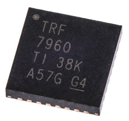
| 描述 | IC RFID FRONT END 13.56MHZ 32QFNRFID应答器 Mulit-Standard High Freq RFid Reader |
| 产品分类 | RFID IC集成电路 - IC |
| 品牌 | Texas Instruments |
| 产品手册 | |
| 产品图片 |
|
| rohs | 符合RoHS无铅 / 符合限制有害物质指令(RoHS)规范要求 |
| 产品系列 | RF集成电路,RFID应答器,Texas Instruments TRF7960RHBT- |
| 数据手册 | |
| 产品型号 | TRF7960RHBT |
| RF类型 | 只读 |
| 产品培训模块 | http://www.digikey.cn/PTM/IndividualPTM.page?site=cn&lang=zhs&ptm=26085 |
| 产品目录页面 | |
| 产品种类 | RFID应答器 |
| 供应商器件封装 | 32-VQFN(5x5) |
| 其它名称 | 296-20793-2 |
| 制造商产品页 | http://www.ti.com/general/docs/suppproductinfo.tsp?distId=10&orderablePartNumber=TRF7960RHBT |
| 功能 | Read Only |
| 包装 | 带卷 (TR) |
| 单位重量 | 71.800 mg |
| 参考设计库 | http://www.digikey.com/rdl/4294959884/4294959883/211 |
| 商标 | Texas Instruments |
| 安装风格 | SMD/SMT |
| 封装 | Reel |
| 封装/外壳 | 32-VFQFN 裸露焊盘 |
| 封装/箱体 | VQFN-32 |
| 工作温度范围 | - 40 C to + 110 C |
| 工厂包装数量 | 250 |
| 最大工作温度 | + 110 C |
| 最小工作温度 | - 40 C |
| 标准包装 | 250 |
| 特性 | ISO14443-A,ISO14443-B,ISO15693,ISO18000-3,Tag-it™ |
| 系列 | TRF7960 |
| 配用 | /product-detail/zh/TRF7960EVM/481-1106-ND/1642574 |
| 频率 | 13.56MHz |


- 商务部:美国ITC正式对集成电路等产品启动337调查
- 曝三星4nm工艺存在良率问题 高通将骁龙8 Gen1或转产台积电
- 太阳诱电将投资9.5亿元在常州建新厂生产MLCC 预计2023年完工
- 英特尔发布欧洲新工厂建设计划 深化IDM 2.0 战略
- 台积电先进制程称霸业界 有大客户加持明年业绩稳了
- 达到5530亿美元!SIA预计今年全球半导体销售额将创下新高
- 英特尔拟将自动驾驶子公司Mobileye上市 估值或超500亿美元
- 三星加码芯片和SET,合并消费电子和移动部门,撤换高东真等 CEO
- 三星电子宣布重大人事变动 还合并消费电子和移动部门
- 海关总署:前11个月进口集成电路产品价值2.52万亿元 增长14.8%


PDF Datasheet 数据手册内容提取
Product Order Technical Tools & Support & Reference Folder Now Documents Software Community Design TRF7960,TRF7961 SLOU186G–AUGUST2006–REVISEDMAY2017 TRF7960, TRF7961 Multiple-Standard Fully Integrated 13.56-MHz RFID Analog Front End and Data-Framing Reader System 1 Device Overview 1.1 Features 1 • CompletelyIntegratedProtocolHandling – SelectableReceiverGain • SeparateInternalHigh-PSRRPowerSuppliesfor – ProgrammableOutputPower(100mWor Analog,Digital,andPASectionsProvideNoise 200mW) IsolationforSuperiorReadRangeandReliability – AdjustableASKModulationRange(8%to30%) • DualReceiverInputsWithAMandPM – Built-InReceiverBand-PassFilterWithUser- DemodulationtoMinimizeCommunicationHoles SelectableCornerFrequencies • ReceiverAMandPMRSSI • WideOperatingVoltageRangeof2.7Vto5.5V • Reader-to-ReaderAnticollision • Ultra-Low-PowerModes • HighIntegrationReducesTotalBOMandBoard – PowerDown: <1 µA Area – Standby:120 µA – SingleExternal13.56-MHzCrystalOscillator – Active(RXOnly):10mA – MCU-SelectableClock-FrequencyOutputofRF, • Parallel8-BitorSerial4-PinSerialPeripheral RF/2,orRF/4 Interface(SPI)WithMCUUsing12-ByteFIFO – Adjustable20-mAHigh-PSRRLDOfor • Ultra-Small32-PinQFNPackage(5mm ×5mm) PoweringExternalMCU • AvailableTools(AlsoSeeToolsandSoftware) • EasytoUseWithHighFlexibility – ReferenceDesignandEVMWithDevelopment – AutomaticallyConfiguredDefaultModesfor Software EachSupportedISOProtocol – SourceCodeAvailablefor MSP430™MCU – 12User-ProgrammableRegisters 1.2 Applications • SecureAccessControl • MedicalSystems • ProductAuthentication • PublicTransportorEventTicketing 1.3 Description The TRF7960 and TRF7961 devices are integrated analog front end and data-framing systems for a 13.56-MHz RFID reader system that supports multiple protocols including ISO/IEC 14443 A and B, FeliCa™, and ISO/IEC 15693. Built-in programming options make it suitable for a wide range of applicationsforproximityandvicinityidentificationsystems. The reader is configured by selecting the desired protocol in the control registers. Direct access to all controlregistersallowsfine-tuningofvariousreaderparametersasneeded. The device supports data rates up to 848 kbps with all framing and synchronization tasks for the ISO protocols onboard. Other standards and even custom protocols can be implemented by using one of the direct modes that the device offers. These direct modes let the application fully control the AFE and also gain access to the raw subcarrier data or the unframed, but already ISO-formatted, data and the associated(extracted)clocksignal. The receiver system has a dual-input receiver architecture to maximize communication robustness. The receivers also include various automatic and manual gain control options. The received signal strength fromtransponders,ambientsources,orinternallevelsisavailableintheRSSIregister. ASPIorparallelinterfacecanbeusedforthecommunicationbetweentheMCUandtheTRF796xreader. Whenthebuilt-inhardwareencodersanddecodersareused,transmitandreceivefunctionsusea12-byte FIFO register. For direct transmit or receive functions, the encoders or decoders can be bypassed so the MCUcanprocessthedatainrealtime. 1 An IMPORTANT NOTICE at the end of this data sheet addresses availability, warranty, changes, use in safety-critical applications, intellectualpropertymattersandotherimportantdisclaimers.PRODUCTIONDATA.
TRF7960,TRF7961 SLOU186G–AUGUST2006–REVISEDMAY2017 www.ti.com The TRF7960 and TRF7961 devices support a wide supply voltage range of 2.7 V to 5.5 V and data communicationlevelsfrom1.8Vto5.5VfortheMCUI/Ointerface. The transmitter has selectable output power levels of 100 mW (+20 dBm) or 200 mW (+23 dBm) equivalent into a 50-Ω load when using a 5-V supply and supports OOK and ASK modulation with selectablemodulationdepth. Built-in programmable auxiliary voltage regulator delivers up to 20 mA to supply an MCU and additional externalcircuitswithinthereadersystem. StartevaluatingtheTRF7960multiprotocoltransceiverICwiththe TRF7960AEVM orthe TRF7960ATB. Documentation, Tools,ReferenceDesigns,andSoftware, Samples DeviceInformation(1) PARTNUMBER PACKAGE BODYSIZE TRF7960RHB VQFN(32) 5mm×5mm TRF7961RHB VQFN(32) 5mm×5mm (1) Formoreinformation,seeSection9,Mechanical,Packaging,and OrderableInformation. 1.4 Typical Application Figure1-1showsatypicalapplicationblockdiagram. VDD_X SYS_CLK VCC Impedance DATA_CLK Matching TX_OUT Circuit TRF796x IRQ MSP430 MCU RX_IN1 RX_IN2 3 (SPI) or 8 (Parallel) OSC_IN OSC_OUT VDD_I/O Crystal 13.56 MHz Copyright © 2017,Texas Instruments Incorporated Figure1-1.ApplicationBlockDiagram 2 DeviceOverview Copyright©2006–2017,TexasInstrumentsIncorporated SubmitDocumentationFeedback ProductFolderLinks:TRF7960 TRF7961
TRF7960,TRF7961 www.ti.com SLOU186G–AUGUST2006–REVISEDMAY2017 Table of Contents 1 DeviceOverview......................................... 1 6.3 Receiver–AnalogSection.......................... 16 .............................................. ................................ 1.1 Features 1 6.4 RegisterDescriptions 22 ........................................... ........... 1.2 Applications 1 6.5 DirectCommandsFromMCUtoReader 31 ............................................ ................... 1.3 Description 1 6.6 ReaderCommunicationInterface 33 ................................... ................... 1.4 Typical Application 2 6.7 ParallelInterfaceCommunication 34 2 Revision History......................................... 4 6.8 SerialInterfaceCommunication..................... 36 3 DeviceComparison ..................................... 5 7 Applications,Implementation,andLayout........ 41 ..................................... ............................. 3.1 RelatedProducts 5 7.1 ApplicationSchematics 41 4 TerminalConfigurationandFunctions.............. 6 8 DeviceandDocumentationSupport............... 43 .......................................... ..................... 4.1 PinDiagram 6 8.1 GettingStartedandNextSteps 43 ................................... ............................... 4.2 SignalDescriptions 6 8.2 Device Nomenclature 43 5 Specifications ............................................ 8 8.3 ToolsandSoftware................................. 44 .......................... ............................. 5.1 AbsoluteMaximumRatings 8 8.4 DocumentationSupport 44 .......................................... ........................................ 5.2 ESDRatings 8 8.5 RelatedLinks 45 ................ .............................. 5.3 RecommendedOperatingConditions 8 8.6 CommunityResources 45 ............................. .......................................... 5.4 ElectricalCharacteristics 8 8.7 Trademarks 45 .................. ..................... 5.5 ThermalResistanceCharacteristics 9 8.8 ElectrostaticDischargeCaution 45 6 DetailedDescription................................... 10 8.9 ExportControlNotice............................... 45 ............................................ ............................................. 6.1 Overview 10 8.10 Glossary 45 6.2 PowerSupplies...................................... 10 9 Mechanical,Packaging,andOrderable Information.............................................. 46 Copyright©2006–2017,TexasInstrumentsIncorporated TableofContents 3 SubmitDocumentationFeedback ProductFolderLinks:TRF7960 TRF7961
TRF7960,TRF7961 SLOU186G–AUGUST2006–REVISEDMAY2017 www.ti.com 2 Revision History NOTE:Pagenumbersforpreviousrevisionsmaydifferfrompagenumbersinthecurrentversion. ChangesfromAugust12,2010toMay18,2017 Page • Removed"andAGC"from"SelectableReceiverGain"inSection1.1,Features ........................................... 1 • Updatedlistofapplications.......................................................................................................... 1 • ChangedcontentsofSection1.3,Description.................................................................................... 1 • AddedDeviceInformationtable .................................................................................................... 2 • AddedSection1.4,TypicalApplication............................................................................................ 2 • AddedSection3,DeviceComparison,andmovedTable3-1toit............................................................. 5 • AddedSection3.1,RelatedProducts ............................................................................................. 5 • ChangedthetitleofSection4fromPhysicalCharacteristicstoTerminalConfigurationandFunctions.................. 6 • RemovedformerSection3.2,PackagingandOrderingInformation(seeSection9,Mechanical,Packaging,and OrderableInformation)............................................................................................................... 7 • Updatednote(1)onSection5.1,AbsoluteMaximumRatings,tostandardwording........................................ 8 • MovedESDratingsfromAbsoluteMaximumRatingstoSection5.2,ESDRatings;changedratingsfrompositive voltagesonlytopositiveandnegative;addednotesforHBMandCDM...................................................... 8 • ChangedformatofMIN,TYP,andMAXcolumnsinSection5.4,ElectricalCharacteristics............................... 8 • Addedthef parameterinSection5.4,ElectricalCharacteristics ..................................................... 9 D_CLKmax • ChangedtitleofandmovedSection5.5,ThermalResistanceCharacteristics.............................................. 9 • MovedcontentsofSection6.1,OverviewfromformerSection2............................................................. 10 • Removedaparagraphthatbegan"Thesecondreceivergainstageanddigitizerstage..."inSection6.3, Receiver–AnalogSection......................................................................................................... 17 • Addedthelastsentencetotheparagraphthatbegins"Thestartofthereceiveoperation(successfullyreceived SOF)..."inSection6.3.2,Receiver–DigitalSection .......................................................................... 18 • Added"andISO/IEC15693"tothefirstsentenceoftheparagraphthatbegins"Theframingsectionalso supportsbit-collisiondetection..."inSection6.3.2,Receiver–DigitalSection............................................. 18 • ChangedB2toReservedinTable6-11,ChipStatusControlRegister(Address=00h) ................................. 23 • ChangedB1andB0toReservedinTable6-22,RXSpecialSettingRegister(Address=0Ah) ........................ 28 • CorrectedthenameoftheResetFIFOcommandinTable6-31,CommandCodes,andSection6.5.2,ResetFIFO 31 • Addedthelastsentencetotheparagraphthatbegins"Theserialcommunicationsworkinthesamemanner..." inSection6.8,SerialInterfaceCommunication................................................................................. 36 • RemovedformersectionExternalPowerAmplifierApplication............................................................... 40 • AddedSection7,Applications,Implementation,andLayout,andmovedtheapplicationschematicstoit............. 41 • AddedSection8,DeviceandDocumentationSupport......................................................................... 43 • AddedSection9,Mechanical,Packaging,andOrderableInformation...................................................... 46 4 RevisionHistory Copyright©2006–2017,TexasInstrumentsIncorporated SubmitDocumentationFeedback ProductFolderLinks:TRF7960 TRF7961
TRF7960,TRF7961 www.ti.com SLOU186G–AUGUST2006–REVISEDMAY2017 3 Device Comparison Table3-1summarizesthedevicecharacteristics. Table3-1.DeviceComparison PROTOCOLS DEVICE ISO/IEC14443AANDB ISO/IEC15693, Tag-it™ 106kbps 212kbps 424kbps 848kbps ISO/IEC18000-3 TRF7960 ✓ ✓ ✓ ✓ ✓ ✓ TRF7961 ✓ ✓ 3.1 Related Products Forinformationaboutotherdevicesinthisfamilyofproductsorrelatedproducts,seethefollowinglinks. ProductsforTIWirelessConnectivity Connect more with the broadest wireless connectivity portfolio in theindustry. ProductsforNFC/RFID TI provides one of the most differentiated NFC and RFID product portfolios in the industry and is your solution to meet a broad range of NFC connectivity and RFID identificationneeds. CompanionProductsforTRF7960 Review products that are frequently purchased or used with this product. ReferenceDesignsforTRF7960 The TI Designs Reference Design Library is a robust reference design library that spans analog, embedded processor, and connectivity. Created by TI experts to help you jump start your system design, all TI Designs include schematic or block diagrams, BOMs, and design files to speed your time to market. Search and download designs at ti.com/tidesigns. Copyright©2006–2017,TexasInstrumentsIncorporated DeviceComparison 5 SubmitDocumentationFeedback ProductFolderLinks:TRF7960 TRF7961
TRF7960,TRF7961 SLOU186G–AUGUST2006–REVISEDMAY2017 www.ti.com 4 Terminal Configuration and Functions 4.1 Pin Diagram Figure4-1showsthepinoutofthe32-pinRHBpackage. D_X C_IN C_OUT S_D S_CLK TA_CLK 2 D S S S N Y A N V O O V E S D E 32 31 30 29 28 27 26 25 VDD_A 1 24 I/O_7 VIN 2 23 I/O_6 VDD_RF 3 22 I/O_5 VDD_PA 4 21 I/O_4 ExposedThermal Pad TX_OUT 5 20 I/O_3 VSS_RF 6 19 I/O_2 VSS_RX 7 18 I/O_1 RX_IN1 8 17 I/O_0 9 10 11 12 13 14 15 16 2 S P K Q D A O RX_IN VS ND_GA SK/OO IR MO VSS_ VDD_I/ A A B Figure4-1.32-PinRHBPackage(TopView) 4.2 Signal Descriptions Table4-1describesthedevicesignals. Table4-1.SignalDescriptions TERMINAL TYPE(1) DESCRIPTION NAME NO. VDD_A 1 OUT Internalregulatedsupply(2.7Vto3.4V)foranalogcircuitry VIN 2 SUP Externalsupplyinputtochip(2.7Vto5.5V) VDD_RF 3 OUT Internalregulatedsupply(2.7Vto5V),normallyconnectedtoVDD_PA(pin4) VDD_PA 4 INP SupplyforPA;normallyconnectedexternallytoVDD_RF(pin3) TX_OUT 5 OUT RFoutput(selectableoutputpower,100mWat8Ωor200mWat4Ω,withV =5V) DD VSS_RF 6 SUP NegativesupplyforPA;normallyconnectedtocircuitground VSS_RX 7 SUP NegativesupplyforRXinputs;normallyconnectedtocircuitground RX_IN1 8 INP RXinput,usedforAMreception RX_IN2 9 INP RXinput,usedforPMreception VSS 10 SUP Chipsubstrateground BAND_GAP 11 OUT Band-gapvoltage(1.6V);internalanalogvoltagereference;mustbeAC-bypassedtoground Alsocanbeconfiguredtoprovidethereceivedanalogsignaloutput(ANA_OUT) ASK/OOK 12 BID Directmode,selectseitherASKorOOKmodulation(0=ASK,1=OOK) IRQ 13 OUT Interruptrequest (1) SUP=Supply,INP=Input,BID=Bidirectional,OUT=Output 6 TerminalConfigurationandFunctions Copyright©2006–2017,TexasInstrumentsIncorporated SubmitDocumentationFeedback ProductFolderLinks:TRF7960 TRF7961
TRF7960,TRF7961 www.ti.com SLOU186G–AUGUST2006–REVISEDMAY2017 Table4-1.SignalDescriptions(continued) TERMINAL TYPE(1) DESCRIPTION NAME NO. MOD 14 INP Directmode,externalmodulationinput VSS_A 15 SUP Negativesupplyforinternalanalogcircuits;normallyconnectedtocircuitground SupplyforI/Ocommunications(1.8Vto5.5V).ShouldbeconnectedtoVINfor5-V VDD_I/O 16 SUP communication,VDD_Xfor3.3-Vcommunication,oranyothervoltagefrom1.8Vto5.5V. I/O_0 17 BID I/Opinforparallelcommunication I/O_1 18 BID I/Opinforparallelcommunication I/O_2 19 BID I/Opinforparallelcommunication I/O_3 20 BID I/Opinforparallelcommunication I/O_4 21 BID I/Opinforparallelcommunication I/Opinforparallelcommunication I/O_5 22 BID Strobeoutclockforserialcommunication Dataclockoutputindirectmode I/Opinforparallelcommunication I/O_6 23 BID MISOforserialcommunication(SPI) Serialbitdataoutputindirectmode1orsubcarriersignalindirectmode0 I/Opinforparallelcommunication. I/O_7 24 BID MOSIforserialcommunication(SPI) Pulseenableandselectionofpower-downmode.IfEN2isconnectedtoVIN,thenVDD_Xis EN2 25 INP activeduringpowerdowntosupporttheMCU.Pincanalsobeusedforpulsewakeupfrom power-downmode. DATA_CLK 26 INP ClockinputforMCUcommunication(parallelandserial) ClockforMCU(3.39/6.78/13.56MHz)atEN=1andEN2=don'tcare SYS_CLK 27 OUT IfEN=0andEN2=1,thensystemclockissetto60kHz EN 28 INP Chipenableinput(IfEN=0,thenchipisinpower-downmode.) VSS_D 29 SUP Negativesupplyforinternaldigitalcircuits;normallyconnectedtocircuitground OSC_OUT 30 OUT Crystaloscillatoroutput OSC_IN 31 INP Crystaloscillatorinput VDD_X 32 OUT Internallyregulatedsupply(2.7Vto3.4V)forexternalcircuitry(MCU) ThermalPad Connectedtocircuitground Copyright©2006–2017,TexasInstrumentsIncorporated TerminalConfigurationandFunctions 7 SubmitDocumentationFeedback ProductFolderLinks:TRF7960 TRF7961
TRF7960,TRF7961 SLOU186G–AUGUST2006–REVISEDMAY2017 www.ti.com 5 Specifications 5.1 Absolute Maximum Ratings overoperatingfree-airtemperaturerange(unlessotherwisenoted)(1) MIN MAX UNIT V Supplyvoltage 6 V IN I Outputcurrent 150 mA O Anycondition 140 T Maximumjunctiontemperature °C J Continuousoperation,long-termreliability(2) 125 T Storagetemperaturerange –55 150 °C stg Leadtemperature 1,6mm(1/16inch)fromcasefor10seconds 300 °C (1) StressesbeyondthoselistedunderAbsoluteMaximumRatingsmaycausepermanentdamagetothedevice.Thesearestressratings only,andfunctionaloperationofthedeviceattheseoranyotherconditionsbeyondthoseindicatedunderrecommendedoperating conditionsisnotimplied.Exposuretoabsolute-maximum-ratedconditionsforextendedperiodsmayaffectdevicereliability. (2) Themaximumjunctiontemperatureforcontinuousoperationislimitedbypackageconstraints.Operationabovethistemperaturemay resultinreducedreliabilityorlifetimeofthedevice. 5.2 ESD Ratings VALUE UNIT Human-bodymodel(HBM),perANSI/ESDA/JEDECJS-001(1) ±2000 V Electrostaticdischarge Charged-devicemodel(CDM),perJEDECspecificationJESD22-C101(2) ±500 V (ESD) Machinemodel(MM) ±200 (1) JEDECdocumentJEP155statesthat500-VHBMallowssafemanufacturingwithastandardESDcontrolprocess.Pinslistedas ±2000Vmayactuallyhavehigherperformance. (2) JEDECdocumentJEP157statesthat250-VCDMallowssafemanufacturingwithastandardESDcontrolprocess.Pinslistedas±500V mayactuallyhavehigherperformance. 5.3 Recommended Operating Conditions overoperatingfree-airtemperaturerange(unlessotherwisenoted) MIN TYP MAX UNIT V Supplyvoltage 2.7 5 5.5 V IN T Operatingvirtualjunctiontemperature –40 125 °C J T Operatingambienttemperature –40 25 110 °C A 5.4 Electrical Characteristics TYPvaluesat25°C,MINandMAXvaluesoveroperatingambienttemperaturerange,V =5V(unlessotherwisenoted) S PARAMETER TESTCONDITIONS MIN TYP MAX UNIT Supplycurrentinpower-down Allsystemsdisabled,includingsupplyvoltage I 1 10 µA PD mode regulators Supplycurrentinpower-down ThereferencevoltagegeneratorandVDD_X I 120 300 µA PD2 mode2 remainactivetosupportexternalcircuitry. Oscillatorrunning,supplyvoltageregulatorsin I Supplycurrentinstandbymode 1.5 4 mA STBY low-consumptionmode Supplycurrentwithoutantenna Oscillator,regulators,RX,andAGCareactive, I 10 16 mA ON1 drivercurrent TXisoff Supplycurrentwithantenna Oscillator,regulators,RX,AGC,andTXare I 70 mA ON2 drivercurrent active,P =100mW out Supplycurrentwithantenna Oscillator,regulators,RX,AGC,andTXareall I 120 mA ON3 drivercurrent active,P =200mW out BG Band-gapvoltage Internalanalogreferencevoltage 1.4 1.6 1.7 V V Power-on-reset(POR)voltage 1.4 2 2.5 V POR Regulatedsupplyforanalog V 3.1 3.5 3.8 V DD_A circuitry 8 Specifications Copyright©2006–2017,TexasInstrumentsIncorporated SubmitDocumentationFeedback ProductFolderLinks:TRF7960 TRF7961
TRF7960,TRF7961 www.ti.com SLOU186G–AUGUST2006–REVISEDMAY2017 Electrical Characteristics (continued) TYPvaluesat25°C,MINandMAXvaluesoveroperatingambienttemperaturerange,V =5V(unlessotherwisenoted) S PARAMETER TESTCONDITIONS MIN TYP MAX UNIT Regulatorsetfor5-Vsystemwith250-mV V RegulatedsupplyforRFcircuitry 4 4.6 5.2 V DD_RF difference Regulatedsupplyforexternal V 3.1 3.4 3.8 V DD_X circuitry Thedifferencebetweentheexternalsupplyand Rejectionofexternalsupplynoise P theregulatedvoltageishigherthan250mV, 20 26 dB PSRR onthesupplyVDD_RFregulator measuredat212kHz Half-powermode 8 12 R PAdriveroutputresistance Ω RFOUT Full-powermode 4 6 RX_IN1andRX_IN2input R 5 10 20 kΩ RFIN resistance V Maximuminputvoltage AtRX_IN1andRX_IN2inputs 3.5 V RFIN PP f =424kHz 1.2 2.5 SUBCARRIER V Inputsensitivity mV SENS PP f =848kHz 1.2 3 SUBCARRIER t Setuptimeafterpowerdown 10 20 ms SET_PD t Setuptimeafterstandbymode 30 100 µs SET_STBY Recoverytimeaftermodulation t Modulationsignal:sine,424kHz,10mVpp 60 µs REC (ISO/IEC14443) f SYS_CLKfrequency InPD2modeEN=0andEN2=1 30 60 120 kHz SYS_CLK DependsoncapacitiveloadontheI/Olines,TI fD_CLKmax MaximumDATA_CLKfrequency recommends2MHz(1) 2 4 8 MHz CLK MaximumCLKfrequency 2 MHz MAX 0.2× 0.2× V Inputlogiclow V IL V V DD_I/O DD_I/O 0.8× V Inputlogichigh V IH V DD_I/O OutputresistanceofI/O_0to R low_io=HforV <2.7V 400 800 Ω OUT I/O_7 DD_I/O R OutputresistanceofSYS_CLK low_io=HforV <2.7V 200 400 Ω SYS_CLK DD_I/O (1) RecommendedDATA_CLKspeedis2MHz;higherdataclockdependsonthecapacitiveload.MaximumSPIclockspeedshouldnot exceed10MHz.Thisclockspeedisacceptableonlywhenexternalcapacitiveloadislessthan30pF.TheMISOdriverhasatypical outputresistanceof400Ω(12-nstimeconstantwhen30-pFloadisused). 5.5 Thermal Resistance Characteristics Rθ Rθ (1) POWERRATING(2) PACKAGE JC JA (°C/W) (°C/W) T ≤25°C T =85°C A A RHB(32) 31 36.4 2.7W 1.1W (1) ThisdatawastakenusingtheJEDECstandardhigh-KtestPCB. (2) Powerratingisdeterminedwithajunctiontemperatureof125°C.Thisisthetemperatureatwhichdistortionstartstoincrease substantially.ThermalmanagementofthefinalPCBshouldstrivetokeepthejunctiontemperatureatorbelow125°Cforbest performanceandlong-termreliability. Copyright©2006–2017,TexasInstrumentsIncorporated Specifications 9 SubmitDocumentationFeedback ProductFolderLinks:TRF7960 TRF7961
TRF7960,TRF7961 SLOU186G–AUGUST2006–REVISEDMAY2017 www.ti.com 6 Detailed Description 6.1 Overview Figure 6-1 shows a typical application diagram for the TRF796x devices. A parallel or serial interface can be implemented for communication between the MCU and reader. Transmit and receive functions use internal encoders and decoders with a 12-byte FIFO register. For direct transmit or receive functions, the encoders and decoders can be bypassed so the MCU can process the data in real time. The transmitter has selectable output power levels of 100 mW (20dBm) or 200 mW (23dBm) into a 50-Ω load (5-V supply) and supports ASK or OOK modulation. Integrated voltage regulators ensure power-supply noise rejectionforthecompletereadersystem. VDD_X SYS_CLK VCC Impedance DATA_CLK Matching TX_OUT Circuit TRF796x IRQ MSP430 MCU RX_IN1 RX_IN2 3 (SPI) or 8 (Parallel) OSC_IN OSC_OUT VDD_I/O Crystal 13.56 MHz Copyright © 2017,Texas Instruments Incorporated Figure6-1.TypicalApplicationDiagram Data transmission supports low-level encoding for ISO/IEC 15693, modified Miller for ISO/IEC 14443 A, high-bit-rate systems for ISO/IEC 14443, and Tag-it coding systems. Included with the data encoding is automaticgenerationofSOF,EOF,CRC,andparitybits. The receiver system enables AM and PM demodulation using a dual-input architecture. The receiver also includes an automatic gain control option and selectable gain. Also included is a selectable bandwidth to cover a broad range of input subcarrier signal options. The received signal strength for AM and PM modulation is accessible through the RSSI register. The receiver output is a digitized subcarrier signal among a selectable protocol and bit rate as outlined in Table 6-13. A selected decoder delivers bit stream andadataclockasoutputs. The receiver system also includes a framing system. This system performs a CRC or parity check, removes the EOF and SOF settings, and organizes the data in bytes. Framed data is then accessible to the MCU through a 12-byte FIFO register and MCU interface. The framing supports ISO/IEC 14443 and ISO/IEC15693protocols. The TRF796x supports data communication levels from 1.8 V to 5.5 V for the MCU I/O interface, while also providing a data synchronization clock. An auxiliary 20-mA regulator (pin 32) is available for additionalsystemcircuits. 6.2 Power Supplies Thepositivesupplypin,VIN(pin2),hasaninputvoltagerangeof2.7Vto5.5V.Thepositivesupplyinput sources three internal regulators with output voltages V , V , and V that use external bypass DD_RF DD_A DD_X capacitors for supply noise filtering. These regulators provide enhanced PSRR for the RFID reader system.Table6-1describesthepowersupplies. 10 DetailedDescription Copyright©2006–2017,TexasInstrumentsIncorporated SubmitDocumentationFeedback ProductFolderLinks:TRF7960 TRF7961
TRF7960,TRF7961 www.ti.com SLOU186G–AUGUST2006–REVISEDMAY2017 The regulators are not independent and have common control bits for output voltage setting. The regulators can be configured to operate in either automatic or manual mode. The automatic regulator mode setting ensures an optimal compromise between regulator PSRR and highest possible supply voltage for RF output power. The manual mode allows the application to manually configure the regulator settings. Table6-1.PowerSupplies SUPPLY DESCRIPTION TheregulatorV (pin3)isusedtosourcetheRFoutputstage.Thevoltageregulatorcanbesetforeither5-Vor3-V DD_RF operation. When configured for 5-V operation, the output voltage can be set from 4.3 V to 5 V in 100-mV steps. The current sourcing V DD_RF capabilityfor5-Voperationis150mAmaximumovertheadjustedoutputvoltagerange. When configured for 3-V operation, the output voltage can be set from 2.7 V to 3.4 V, also in 100-mV steps. The current sourcingcapabilityfor3-Voperationis100mAmaximumovertheadjustedoutputvoltagerange. RegulatorV (pin1)suppliesvoltagetoanalogcircuitswithinthereaderchip.Thevoltagesettingisdividedintworanges. DD_A Whenconfiguredfor5-Voperation,theoutputvoltageisfixedat3.5V.Whenconfiguredfor3-Voperation,theoutputvoltage VDD_A canbesetfrom2.7Vto3.4Vin100-mVsteps. NOTE:TheV andV regulatorsareconfiguredtogether(theirsettingsarenotindependent). DD_A DD_X RegulatorV (pin32)canbeusedtosourcethedigitalI/Oofthereaderchiptogetherwithotherexternalsystem DD_X components.Whenconfiguredfor5-Voperation,theoutputvoltageisfixedat3.4V.Whenconfiguredfor3-Voperation,the outputvoltagecanbesetfrom2.7to3.4Vin100-mVsteps. V DD_X ThetotalcurrentsourcingcapabilityoftheV regulatoris20mA(maximum)overtheadjustedoutputrange. DD_X NOTE:TheV andV regulatorsareconfiguredtogether(theirsettingsarenotindependent). DD_A DD_X TheV pin(pin4)isthepositivesupplypinfortheRFoutputstageandisexternallyconnectedtotheregulatoroutput V DD_PA DD_PA V (pin3). DD_RF 6.2.1 Negative Supply Connections Thenegativesupplyconnectionsareallexternallyconnectedtogether(toGND).Thesubstrateconnection is V (pin 10), the analog negative supply is V (pin 15), the logic negative supply is V (pin 29), SS SS_A SS_D the RF output stage negative supply is V (pin 6), and the negative supply for the RF receiver input is SS_TX V (pin7). SS_RX 6.2.2 Digital I/O Interface To allow compatible I/O signal levels, the TRF796x has a separate supply input V (pin 16), with an DD_I/O input voltage range of 1.8 V to 5.5 V. This pin supplies the I/O interface (I/O_0 to I/O_7), IRQ, SYS_CLK, and DATA_CLK pins of the reader. In typical applications, V is connected directly to V to ensure DD_I/O DD_X thattheI/OsignallevelsoftheMCUarethesameastheinternallogiclevelsofthereader. 6.2.3 Supply Regulator Configuration The supply regulators can be automatically or manually configured by the control bits. Table 6-2 lists the manual regulator settings for a 5-V system. Table 6-3 lists the manual regulator settings for a 3-V system. Table6-4andTable6-5listtheautomaticmodegainsettingsfor5-Vand3-Vsystems,respectively. The automatic mode is the default configuration. In automatic mode, the regulators are automatically set every time the system is activated by asserting the EN input high. The internal regulators are also automaticallyreconfiguredeverytimetheautomaticregulatorselectionbitissethigh(ontherisingedge). Copyright©2006–2017,TexasInstrumentsIncorporated DetailedDescription 11 SubmitDocumentationFeedback ProductFolderLinks:TRF7960 TRF7961
TRF7960,TRF7961 SLOU186G–AUGUST2006–REVISEDMAY2017 www.ti.com The application can reset the automatic mode setting from a state in which the automatic setting bit is already high by changing the automatic setting bit from high to low to high. The regulator-configuration algorithm adjusts the regulator outputs 250 mV below the V level, but not higher than 5 V for V , 3.5 IN DD_RF V for V , and 3.4 V for V . This algorithm ensures the highest possible supply voltage for the RF DD_A DD_X output stage while maintaining an adequate PSRR (power supply rejection ratio). As an example, the application can improve the PSRR if there is a noisy supply voltage from V by increasing the target DD_X voltage difference across the V regulator as listed for automatic regulator settings in Table 6-4 and DD_X Table6-5. Table6-2.Supply-RegulatorSetting – Manual– 5-VSystem BYTE OPTIONBITSSETTINGINCONTROLREGISTER ACTION ADDRESS B7 B6 B5 B4 B3 B2 B1 B0 0x00 1 5-Vsystem 0x0B 0 Manualregulatorsetting 0x0B 0 1 1 1 V =5V,V =3.5V,V =3.4V DD_RF DD_A DD_X 0x0B 0 1 1 0 V =4.9V,V =3.5V,V =3.4V DD_RF DD_A DD_X 0x0B 0 1 0 1 V =4.8V,V =3.5V,V =3.4V DD_RF DD_A DD_X 0x0B 0 1 0 0 V =4.7V,V =3.5V,V =3.4V DD_RF DD_A DD_X 0x0B 0 0 1 1 V =4.6V,V =3.5V,V =3.4V DD_RF DD_A DD_X 0x0B 0 0 1 0 V =4.5V,V =3.5V,V =3.4V DD_RF DD_A DD_X 0x0B 0 0 0 1 V =4.4V,V =3.5V,V =3.4V DD_RF DD_A DD_X 0x0B 0 0 0 0 V =4.3V,V =3.5V,V =3.4V DD_RF DD_A DD_X Table6-3.Supply-RegulatorSetting – Manual– 3-VSystem BYTE OPTIONBITSSETTINGINCONTROLREGISTER ACTION ADDRESS B7 B6 B5 B4 B3 B2 B1 B0 0x00 0 3-Vsystem 0x0B 0 Manualregulatorsetting 0x0B 0 1 1 1 V =3.4V,V ,V =3.4V DD_RF DD_A DD_X 0x0B 0 1 1 0 V =3.3V,V ,V =3.3V DD_RF DD_A DD_X 0x0B 0 1 0 1 V =3.2V,V ,V =3.2V DD_RF DD_A DD_X 0x0B 0 1 0 0 V =3.1V,V ,V =3.1V DD_RF DD_A DD_X 0x0B 0 0 1 1 V =3.0V,V ,V =3.0V DD_RF DD_A DD_X 0x0B 0 0 1 0 V =2.9V,V ,V =2.9V DD_RF DD_A DD_X 0x0B 0 0 0 1 V =2.8V,V ,V =2.8V DD_RF DD_A DD_X 0x0B 0 0 0 0 V =2.7V,V ,V =2.7V DD_RF DD_A DD_X Table6-4.Supply-RegulatorSetting – Automatic –5-VSystem BYTE OPTIONBITSSETTINGINCONTROLREGISTER ACTION ADDRESS B7 B6 B5 B4 B3 B2(1) B1 B0 0x00 1 5-Vsystem 0x0B 1 x 1 1 Automaticregulatorsetting;approximately250-mVdifference 0x0B 1 x 1 0 Automaticregulatorsetting;approximately350-mVdifference 0x0B 1 x 0 0 Automaticregulatorsetting;approximately400-mVdifference (1) x=Don'tcare 12 DetailedDescription Copyright©2006–2017,TexasInstrumentsIncorporated SubmitDocumentationFeedback ProductFolderLinks:TRF7960 TRF7961
TRF7960,TRF7961 www.ti.com SLOU186G–AUGUST2006–REVISEDMAY2017 Table6-5.Supply-RegulatorSetting – Automatic –3-VSystem BYTE OPTIONBITSSETTINGINCONTROLREGISTER ACTION ADDRESS B7 B6 B5 B4 B3 B2(1) B1 B0 0x00 0 3-Vsystem 0x0B 1 x 1 1 Automaticregulatorsetting;approximately250-mVdifference 0x0B 1 x 1 0 Automaticregulatorsetting;approximately350-mVdifference 0x0B 1 x 0 0 Automaticregulatorsetting;approximately400-mVdifference (1) x=Don'tcare 6.2.4 Power Modes The chip has seven power states, which are controlled by two input pins (EN and EN2) and three bits in theChipStatusControlregister(00h). The main reader enable input is EN (which has a threshold level of 1 V [minimum]). Any input signal level from1.8VtoV canbeused.WhenENissethigh,allofthereaderregulatorsareenabled,togetherwith IN the13.56-MHzoscillator,andtheSYS_CLKoutputclockforanexternalMCU. TheauxiliaryenableinputEN2hastwofunctions: • A direct connection from EN2 to V ensures availability of the regulated supply (V ) and an IN DD_X auxiliary clock signal (60 kHz) on the SYS_CLK output (same for the case EN = 0). This mode is intended for systems in which the MCU controlling the reader is also being supplied by the reader supplyregulator(V )andtheMCUclockissuppliedbytheSYS_CLKoutputofthereader.Thislets DD_X theMCUsupplyandclockbeavailableduringpowerdown. • EN2 enables start-up of the reader system from complete power down (EN = 0, EN2 = 0). In this case, the EN input is controlled by the MCU or other system device that is without supply voltage during complete power down (thus unable to control the EN input). A rising edge applied to the EN2 input (which has a 1-V threshold level) starts the reader supply system and 13.56-MHz oscillator (identical to condition EN = 1). This start-up mode lasts until all of the regulators have settled and the 13.56-MHz oscillator has stabilized. If the EN input is set high by the MCU (or other system device), the reader stays active. If the EN input is not set high within 100 µs after the SYS_CLK output is switched from auxiliary clock (60 kHz) to high-frequency clock (derived from the crystal oscillator), the reader system returns to a complete power-down mode. This option can be used to wake the reader system from completepowerdownbyusingapush-buttonswitchorbysendingasinglepulse. After the reader EN line is high, the other power modes are selected by control bits. Table 6-6 lists the powermodeoptionsandfunctions. Copyright©2006–2017,TexasInstrumentsIncorporated DetailedDescription 13 SubmitDocumentationFeedback ProductFolderLinks:TRF7960 TRF7961
TRF7960,TRF7961 SLOU186G–AUGUST2006–REVISEDMAY2017 www.ti.com Table6-6.PowerModes OPTIONBITSSETTINGINCHIPSTATUSCONTROL BYTE REGISTER EN EN2 FUNCTIONALITY CURRENT ADDRESS B7 B5 B3 B1 B6 B4 B2 B0 stby rfon rf_pwr rec_on 0x00 0 0 Completepowerdown <1µA VDD_Xavailable, 0x00 0 1 SYS_CLKauxiliaryfrequency 120µA 60kHzisON Allsupplyregulatorsactiveandin lowpowermode, 0x00 1 x x x 1 x 1.5mA 13.56-MHzoscillatoron, SYS_CLKclockavailable Allsupplyregulatorsactive, 0x00 0 0 x 0 1 x 13.56-MHzoscillatoron, 3.5mA SYS_CLKclockavailable Allsupplyregulatorsactive, 13.56-MHzoscillatoron, 0x00 0 0 x 1 1 x 10mA SYS_CLKclockavailable, Receiveractive Allsupplyregulatorsactive, 13.56-MHzoscillatoron, SYS_CLKclockavailable, 70mA 0x00 0 1 1 x 1 x Receiveractive, (at5V) Transmitteractiveinhalf-power mode Allsupplyregulatorsactive, 13.56-MHzoscillatorrunning, SYS_CLKclockavailable, 120mA 0x00 0 1 0 x 1 x Receiveractive, (at5V) Transmitteractiveinfull-power mode During reader inactivity, the TRF796x can be placed in power-down mode (EN = 0). The power down can be complete (EN = 0, EN2 = 0) with no function running, or partial (EN = 0, EN2 = 1) with the regulated supply(V )and60-kHzauxiliaryclock(SYS_CLK)availabletotheMCUorothersystemdevice. DD_X When EN is set high (or on rising edge of EN2 and then confirmed by EN = 1), the supply regulators are activated and the 13.56-MHz oscillator is started. When the supplies are settled and the oscillator frequency is stable, the SYS_CLK output is switched from the auxiliary frequency of 60 kHz to the selectedfrequencyderivedfromthecrystaloscillator.Atthistime,thereaderisreadytocommunicateand perform the required tasks. The control system (MCU) can then write appropriate bits to the Chip Status Controlregister(address0x00)andselecttheoperationmode. The standby mode (bit 7 = 1 in register 0x00) is the active mode with the lowest current consumption. The readercanrecoverfromthismodetofulloperationin100 µs. The active mode with RF section disabled (bit 5 = 0 and bit 1 = 0 in register 0x00) is the next active mode withlowpowerconsumption.Thereaderiscapableofrecoveringfromthismodetofulloperationin25 µs. The active mode with only the RF receiver section active (bit 1 = 1 in register 0x00) can be used to measuretheexternalRFfield(seeSection6.3.1)ifreader-to-readeranticollisionisimplemented. The active mode with the entire RF section active (bit 5 = 1 in register 0x00) is the normal mode used for transmitandreceiveoperations. 6.2.5 Timing Diagrams Figure6-2showsanoscilloscopetraceofchippowerup. Figure6-3showsanoscilloscopetraceofchipenabletoclockstartwithEN2lowandENhigh. Figure6-4showsanoscilloscopetraceofchipenabletoclockstartwithEN2highandENlow. 14 DetailedDescription Copyright©2006–2017,TexasInstrumentsIncorporated SubmitDocumentationFeedback ProductFolderLinks:TRF7960 TRF7961
TRF7960,TRF7961 www.ti.com SLOU186G–AUGUST2006–REVISEDMAY2017 Figure6-2.ChipPowerUp[V (Blue)toCrystalStart(Red)] IN Figure6-3.ChipEnabletoClockStart,EN2LowandENHigh(Blue)toStartofSystemClock(Red) Copyright©2006–2017,TexasInstrumentsIncorporated DetailedDescription 15 SubmitDocumentationFeedback ProductFolderLinks:TRF7960 TRF7961
TRF7960,TRF7961 SLOU186G–AUGUST2006–REVISEDMAY2017 www.ti.com Figure6-4.ChipEnabletoClockStart,EN2HighandENLow(Blue)toStartofSystemClock(Red) 6.3 Receiver – Analog Section The TRF796x has two receiver inputs, RX_IN1 (pin 8) and RX_IN2 (pin 9). The two inputs are connected to an external filter to ensure that AM modulation from the tag is available on at least one of the two inputs. The external filter provides a 45° phase shift for the RX_IN2 input to allow further processing of a received PM-modulated signal (if it appears) from the tag. This architecture eliminates any possible communicationholesthatmayoccurfromthetagtothereader. The two RX inputs are multiplexed to two receiver channels: the main receiver and the auxiliary receiver. Receiver input multiplexing is controlled by control bit B3 (pm_on) in the Chip Status Control register (address 0x00). The main receiver is composed of an RF-detection stage, gain, filtering with AGC, and a digitizing stage whose output is connected to the digital processing block. The main receiver also has an RSSImeasuringstage,whichmeasuresthestrengthofthedemodulatedsignal. The primary function of the auxiliary receiver is to measure the RSSI of the modulation signal. It also has similarRF-detection,gain,filteringwithAGC,andRSSIblocks. The default setting is RX_IN1 connected to the main receiver and RX_IN2 connected to the auxiliary receiver (bit pm_on = 0). When a response from the tag is detected by the RSSI, values on both inputs are measured and stored in the RSSI Level register (address 0x0F). The control system reads the RSSI valuesandswitchestothestrongerreceiverinput(RX_IN1orRX_IN2bysettingpm_on=1). The receiver input stage is an RF level detector. The RF amplitude level on RX_IN1 and RX_IN2 inputs should be approximately 3 V for a V supply level greater than 3.3 V. If the V level is lower, the RF PP IN IN input peak-to-peak voltage level should not exceed the V level. V is the main supply voltage to the IN IN deviceatpin2. The first gain and filtering stage following the RF-envelope detector has a nominal gain of 15 dB with an adjustable band-pass filter. The band-pass filter has adjustable 3-dB frequency steps (100 kHz to 400 kHz for high pass and 600 kHz to 1500 kHz for low pass). Following the band-pass filter is another gain-and- filteringstagewithanominalgainof8dBandwithfrequencycharacteristicsidenticaltothefirststage. 16 DetailedDescription Copyright©2006–2017,TexasInstrumentsIncorporated SubmitDocumentationFeedback ProductFolderLinks:TRF7960 TRF7961
TRF7960,TRF7961 www.ti.com SLOU186G–AUGUST2006–REVISEDMAY2017 The internal filters are configured automatically, with internal presets for each new selection of a communication standard in the ISO Control register (address 0x01). If required, additional fine-tuning can be accomplished by writing directly to the RX Special Setting register (address 0x0A). Table 6-22 lists the bitsoftheRXSpecialSettingsregister(address0x0A)thatcontrolthereceiveranalogsection. 6.3.1 Received Signal Strength Indicator (RSSI) The RSSI measurement block measures the demodulated signal (except in the case of a direct command for RF-amplitude measurement; see Section 6.5). The measuring system latches the peak value, so the RSSI level can be read after the end of the receive packet. The RSSI register values reset with every transmissionbythereader.ThisallowsanupdatedRSSImeasurementforeachnewtagresponse. Table 6-7 and Table 6-8 list the correlation between the RF input level and RSSI designation levels on RX_IN1andRX_IN2. Table 6-7 compares the RSSI level and the RSSI bit value. The RSSI has seven levels (3 bits each) with 4-dB increments. The input level is the peak-to-peak modulation level of the RF signal as measured on onesideenvelope(positiveornegative). Table6-7.RSSILevelVersusRegisterBitValue RSSI 1 2 3 4 5 6 7 Inputlevel 2mVpp 3.2mVpp 5mVpp 8mVpp 13mVpp 20mVpp 32mVpp Asanexample,fromTable6-8,letB2=1,B1=1,B0=0.ThisyieldsanRSSIvalueof6.FromTable6-7 abitvalueof6indicatesanRSSIlevelof20mVpp. Table6-8.RSSIBitValueandOscillatorStatusRegister(0x0F) BIT SIGNAL FUNCTION COMMENTS B7 Unused B6 osc_ok Crystaloscillatorstable B5 rssi_x2 Mostsignificantbit(MSB)ofauxiliaryreceiverRSSI B4 rssi_x1 AuxiliaryreceiverRSSI 4dBperstep B3 rssi_x1 Leastsignificantbit(LSB)ofauxiliaryreceiverRSSI B2 rssi_2 MSBofmainreceiverRSSI B1 rssi_1 MainreceiverRSSI 4dBperstep B0 rssi_0 LSBofmainreceiverRSSI 6.3.2 Receiver – Digital Section The received subcarrier is digitized to form a digital representation of the modulated RF envelope. This digitizedsignalisappliedtodigitaldecodersandframingcircuitsforfurtherprocessing. The digital part of the receiver consists of two sections, which partly overlap. The first section consists of the bit decoders for the various protocols, and the second section consists of the framing logic. The bit decoders convert the subcarrier coded signal to a bit stream and also to the data clock. Thus, the subcarrier-coded signal is transformed to serial data, and the data clock is extracted. The decoder logic is designed for maximum error tolerance. This enables the decoders to successfully decode even partly corrupted(duetonoiseorinterference)subcarriersignals. In the framing section, the serial bit stream data is formatted in bytes. In this process, special signals like the start of frame (SOF), end of frame (EOF), start of communication, and end of communication are automatically removed. The parity bits and CRC bytes are checked and also removed. The end result is clean or raw data, which is sent to the 12-byte FIFO register where it can be read by the external microcontrollersystem. Copyright©2006–2017,TexasInstrumentsIncorporated DetailedDescription 17 SubmitDocumentationFeedback ProductFolderLinks:TRF7960 TRF7961
TRF7960,TRF7961 SLOU186G–AUGUST2006–REVISEDMAY2017 www.ti.com The start of the receive operation (successfully received SOF) sets the flags in the IRQ Status register. Theendofthereceiveoperationisindicatedtotheexternalsystem(MCU)bysendinganinterruptrequest (pin 13, IRQ). If the receive data packet is longer than 8 bytes, an interrupt is sent to the MCU when the received data occupies 75% of the FIFO capacity to signal that the data should be removed from the FIFO. Use the FIFO Status register (0x1C) to provide the number of bytes that should be clocked out duringtheactualFIFOread. If any error in data format, parity, or CRC is detected, the external system is notified of the error by an interrupt-request pulse. The source condition of the interrupt-request pulse is available in the IRQ Status register(address0x0C)(seeTable6-24). TheISOControlregister(address0x01)istheprimarycontrolforthedigitalpartofthereceiver.Bywriting to this register, the application selects the protocol to be used. With each new write in this register, the default presets are loaded in all related registers, so no further adjustments in other registers are typically neededforproperoperation. Table 6-12 describes the coding of the ISO Control register. The TRF7961 does not include the ISO/IEC 14443 functionality; therefore, the features and commands for this protocol are not functional for theTRF7961. The framing section also supports bit-collision detection as specified in ISO/IEC 14443 A and ISO/IEC 15693. When a bit collision is detected, an interrupt request is sent and a flag is set in the IRQ Status register. For ISO/IEC 14443 A specifically, the position of the bit collision is written in two registers: partly in the Collision Position register (0x0E) and partly in the Collision Position and Interrupt Mask register (0x0D) (bits B6 and B7). The collision position is presented as a sequential bit number, where the count starts immediately after the start bit. For example, the collision in the first bit of the UID would give the value 00 0001 0000 in the collision position registers. The count starts with 0, and the first 16 bits are thecommandcodeandtheNVBbyte(theNVBbyteisthenumberofvalidbits). The receive section also has two timers. The RX wait time timer is controlled by the value in the RX Wait Time register (address 0x08). This timer defines the time after the end of the transmit operation in which the receive decoders are not active (held in reset state). This prevents incorrect detections resulting from transients following the transmit operation. The value of the RX Wait Time register defines this time in increments of 9.44 µs. This register is preset at every write to ISO Control register (address 0x01) accordingtotheminimumtag-responsetimedefinedbyeachstandard. The RX no response timer is controlled by the RX No Response Wait Time register (address 0x07). This timermeasuresthetimefromthestartofslotintheanticollisionsequenceuntilthestartoftagresponse.If there is no tag response in the defined time, an interrupt request is sent and a flag is set in IRQ Status Control register. This enables the external controller to be relieved of the task of detecting empty slots. The wait time is stored in the register in increments of 37.76 µs. This register is also preset, automatically, foreverynewprotocolselection. 6.3.3 Transmitter The transmitter section consists of the 13.56-MHz oscillator, digital protocol processing, and RF output stage. 6.3.3.1 Transmitter–AnalogSection The13.56-MHzcrystaloscillator(connectedtopins31and32)directlygeneratestheRFfortheRFoutput stage. It also generates the clock signal for the digital section and the clock signal output on SYS_CLK (pin27),whichcanbeusedbyanexternalMCUsystem. During partial power-down mode (EN = 0, EN2 = 1), the frequency of SYS_CLK is 60 kHz. During normal reader operation, SYS_CLK can be programmed by bits B4 and B5 in the Modulator and SYS_CLK Controlregister(address0x09);availableclockfrequenciesare13.56MHz,6.78MHz,or3.39MHz. Table6-9liststherecommendationsforthereferencecrystal(HC49U). 18 DetailedDescription Copyright©2006–2017,TexasInstrumentsIncorporated SubmitDocumentationFeedback ProductFolderLinks:TRF7960 TRF7961
TRF7960,TRF7961 www.ti.com SLOU186G–AUGUST2006–REVISEDMAY2017 Table6-9.CrystalRecommendations PARAMETER SPECIFICATION Frequency 13.560000MHz Modeofoperation Fundamental Typeofresonance Parallel Frequencytolerance ±20ppm Aging <5ppm/year Operationtemperaturerange –40°Cto85°C Equivalentseriesresistance 50Ω,minimum NOTE Thevalueofthetwoexternalshuntcapacitorsonthecrystaloscillatoriscalculatedbasedon thespecified loadcapacitanceof thecrystal. The externalcapacitors(connectedto theOSC pins 30 and 31), are calculated as two capacitors in series plus C (the internal I/O S capacitance of the oscillator gate plus PCB stray capacitance). The stray capacitance (C ) S canbeestimatedat5±2pF(typical). Asanexample,givenacrystalwitharequiredloadcapacitance(C )of18pF, L C =((C ×C )/(C +C ))+C L 1 2 1 2 S 18pF=((27pF×27pF)/(27pF+27pF))+4.5pF From this example, 18-pF capacitors would be placed on pins 30 and 31 to ensure proper crystaloscillatoroperation. The transmit power level is selectable as either half power of 100 mW (20 dBm) or full power of 200 mW (23 dBm) when configured for 5-V automatic operation. The transmit output impedance is 8 Ω when configured for half power and 4 Ω when configured for full power. Selection of the transmit power level is set by bit B4 (rf_pwr) in the Chip Status Control register (see Table 6-11). When configured for 3-V automatic operation, the transmit power level is typically selectable as either 33 mW (15 dBm) in half- power mode or 70 mW (18 dBm) in full-power mode (VDD_RF at 3.3 V). Lower operating voltages result inreducedtransmitpowerlevels. In typical operation, the transmit modulation is configured by the selected ISO Control register (address 0x01). External control of the transmit modulation is possible by setting the ISO Control register (address 0x01) to direct mode. While in direct mode, the transmit modulation is set by the ASK/OOK pin (pin 12). External control of the modulation type is enabled by setting B6 = 1 (en_ook_p) in the Modulator and SYS_CLK Control register (address 0x09). ASK modulation depth is controlled by bits B0, B1, and B2 in the Modulator and SYS_CLK Control register (address 0x09). The range of the ASK modulation is 7% to 30%,or100%(OOK). Table6-21describesthecodingoftheModulatorandSYS_CLKControlregister. The length of the modulation pulse is defined by the protocol selected in the ISO Control register. With a high-Q antenna, the modulation pulse is typically prolonged, and the tag detects a longer pulse than intended. For such cases, the modulation pulse length can be corrected by using the TX Pulse Length register.Iftheregistercontainsallzeros,thenthepulselengthisgovernedbytheprotocolselection.Ifthe register contains a value other than 00h, the pulse length is equal to the value of the register in 73.7-ns increments.Thismeanstherangeofadjustmentis73.7nsto18.8 µs. Copyright©2006–2017,TexasInstrumentsIncorporated DetailedDescription 19 SubmitDocumentationFeedback ProductFolderLinks:TRF7960 TRF7961
TRF7960,TRF7961 SLOU186G–AUGUST2006–REVISEDMAY2017 www.ti.com 6.3.3.2 Transmitter–DigitalSection The digital portion of the transmitter is very similar to that of the receiver. Before beginning data transmission, the FIFO should be cleared with a Reset command (0x0F). Data transmission is initiated withaselectedcommand(seeTable6-31).TheMCUthencommandsthereadertodoacontinuousWrite command(3Dh,seeTable6-33)startingfromregister1Dh.Datawrittenintoregister1DhistheTXLength Byte1 (upper and middle nibbles), while the following byte in register 1Eh is the TX Length Byte2 (lower nibbleandbrokenbytelength).TheTXbytelengthdetermineswhenthereadersendstheEOFbyte.After the TX length bytes, FIFO data is loaded in register 1Fh with byte storage locations 0 to 11. Data transmission begins automatically after the first byte is written into the FIFO. The TX Length bytes and FIFOcanbeloadedwithacontinuous-writecommandbecausetheaddressesaresequential. IfthedatalengthislongerthantheallowablesizeoftheFIFO,theexternalsystem(MCU)iswarnedwhen the majority of data from the FIFO has already been transmitted by sending an interrupt request with a flag in the IRQ register signaling FIFO low or high status. The external system should respond by loading thenextdatapacketintotheFIFO. At the end of the transmit operation, the external system is notified by another interrupt request with a flag intheIRQregisterthatsignalstheendofTX. The TX Length register also supports incomplete bytes transmitted. The high 2 nibbles in register 0x1D and the nibble composed of bits B4 to B7 in register 0x1E store the number of complete bytes to be transmitted. Bit 0 (in register 0x1E) is a flag that signals the presence of additional bits to be transmitted that do not form a complete byte. The number of bits are stored in bits B1 to B3 of the same register (0x1E). The protocol is selected by the ISO Control register (address 0x01), which also selects the receiver protocol. As defined by the selected protocol, the reader automatically adds all the special signals, like start of communication, end of communication, SOF, EOF, parity bits, and CRC bytes. The data is then codedtothemodulationpulselevelandsenttothemodulationcontroloftheRFoutputstage.Thismeans that the external system is only required to load the FIFO with data, and all the low-level coding is done automatically. Also, all registers used in transmission are automatically preset to the optimum value when anewselectionisenteredintotheISOControlregister. Some protocols have options, and two registers are provided to select the TX protocol options. The first register is ISO14443B TX Options (address 0x02). This register controls the SOF and EOF selection and EGT(extraguardtime)selectionfortheISO/IEC14443Bprotocol(seeTable6-14) The second register controls the ISO/IEC 14443 high-bit-rate options. This register enables the use of differentbitratesforRXandTXoperationsintheISO/IEC14443highbit-rateprotocol.Additionally,italso selectstheparitysystemfortheISO/IEC14443Ahigh-bit-rateselection(seeTable6-15). The transmit section also has a timer that can be used to start the transmit operation at a precise time interval from a selected event. This is necessary if the tag requires a reply in an exact window of time following the tag response. The TX timer uses two registers (addresses 0x04 and 0x05). In first register (address 0x04), two bits (B7 and B6) define the trigger conditions. The remaining 6 bits are the upper bits and the 8 bits in register address 0x05 are lower bits, which are preset to the counter. The increment is 590 ns and the range of this counter is from 590 ns to 9.7 ms. See Table 6-16 for the bit definitions (triggerconditions). 6.3.4 Direct Mode Directmodesupportstwoconfigurations: Direct mode 0 (bit 6 = 0 in the ISO Control register) enables use of only the front-end functions of the reader, bypassing the protocol implementation in the reader. For transmit functions, the application has direct access to the transmit modulator through the MOD pin (pin 14). On the receive side, the application hasdirectaccesstothesubcarriersignal(digitizedRFenvelopesignal)onI/O_6(pin23). 20 DetailedDescription Copyright©2006–2017,TexasInstrumentsIncorporated SubmitDocumentationFeedback ProductFolderLinks:TRF7960 TRF7961
TRF7960,TRF7961 www.ti.com SLOU186G–AUGUST2006–REVISEDMAY2017 Direct mode 1 (bit 6 = 1 in the ISO Control register) uses the subcarrier signal decoder of the selected protocol (as defined in the ISO Control register). This means that the receive output is not the subcarrier signalbutthedecodedserialbitstreamandbitclocksignals.TheserialdataisavailableonI/O_6(pin23) and the bit clock is available on I/O_5 (pin 22). The transmit side is identical; the application has direct control over the RF modulation through the MOD input. This mode is provided so that the application can implement a protocol that has the same bit coding as one of the protocols implemented in the reader, but needsadifferentframingformat. To use direct mode, first select the direct mode to enter by writing B6 in the ISO Control register. This bit determines if the receive output is the direct subcarrier signal (B6 = 0) or the serial data of the selected decoder. If B6 = 1, also define which protocol should be used for bit decoding by writing the appropriate settingintheISOControlregister. The reader actually enters the direct mode when B6 (direct) is set to 1 in the Chip Status Control register. Direct mode starts immediately. The write command should not be terminated with a stop condition (see communication protocol), because the stop condition terminates the direct mode and clears B6. This is necessary as the direct mode uses one or two I/O pins (I/O_6, I/O_5). Standard parallel communication is notpossibleindirectmode.Sendingastopconditionterminatesdirectmode. Figure6-5showsmode0andmode1indirectmode. • Inmode0,thereaderisusedasanAFEonly,andprotocolhandlingisbypassed. • In mode 1, framing is not done, but SOF and EOF are present. This allows for a user-selectable framinglevelbasedonanexistingISOstandard. In mode 2 (standard mode), data is ISO-standard formatted. SOF, EOF, and error checking are removed, sothemicroprocessorreceivesonlybytesofrawdatathrougha12-byteFIFO. Analog Front End (AFE) Mode 0: Raw subcarrier data ISO Encoders and Decoders 14443A 14443B 15693 Tag-it Mode 1: Unframed raw ISO formatted data Packetization and Framing Mode 2:Full ISO with framing and error checking(typical mode) Figure6-5.User-ConfigurableModes Copyright©2006–2017,TexasInstrumentsIncorporated DetailedDescription 21 SubmitDocumentationFeedback ProductFolderLinks:TRF7960 TRF7961
TRF7960,TRF7961 SLOU186G–AUGUST2006–REVISEDMAY2017 www.ti.com 6.3.5 Register Preset After power up and the EN pin low-to-high transition, the reader is in the default mode. The default configurationisISO/IEC15693,singlesubcarrier,highdatarate,1-out-of-4operation.Thelow-leveloption registers (0x02 to 0x0B) are automatically set to adapt the circuitry optimally to the appropriate protocol parameters. When entering another protocol (writing to the ISO Control register [0x01]), the low-level option registers (0x02to0x0B)areautomaticallyconfiguredtothenewprotocolparameters. After selecting the protocol, it is possible to change some low-level register contents if needed. However, changing to another protocol and then back, reloads the default settings, and the application must reload thecustomsettings. The Clo1 and Clo0 bits in register 0x09, which define the microcontroller frequency available on the SYS_CLK pin, are the only two bits in the configuration registers that are not cleared during protocol selection. 6.4 Register Descriptions Table6-10liststheregistersbyaddress. Table6-10.RegisterAddressSpace ADDRESS REGISTER READ/WRITE DETAILS MainControlRegisters 0x00 Chipstatuscontrol R/W Table6-11 0x01 ISOcontrol R/W Table6-12 ProtocolSubsettingRegisters 0x02 ISO14443BTXoptions R/W Table6-14 0x03 ISO14443Ahighbitrateoptions R/W Table6-15 0x04 TXtimersetting,H-byte R/W Table6-16 0x05 TXtimersetting,L-byte R/W Table6-17 0x06 TXpulse-lengthcontrol R/W Table6-18 0x07 RXnoresponsewait R/W Table6-19 0x08 RXwaittime R/W Table6-20 0x09 ModulatorandSYS_CLKcontrol R/W Table6-21 0x0A RXspecialsetting R/W Table6-22 0x0B RegulatorandI/Ocontrol R/W Table6-23 0x16 Unused NA 0x17 Unused NA 0x18 Unused NA 0x19 Unused NA StatusRegisters 0x0C IRQstatus R Table6-24 0x0D Collisionpositionandinterruptmaskregister R/W Table6-25 0x0E Collisionposition R Table6-26 0x0F RSSIlevelsandoscillatorstatus R Table6-27 FIFORegisters 0x1C FIFOstatus R Table6-28 0x1D TXlengthbyte1 R/W Table6-29 0x1E TXlengthbyte2 R/W Table6-30 0x1F FIFOI/Oregister R/W 22 DetailedDescription Copyright©2006–2017,TexasInstrumentsIncorporated SubmitDocumentationFeedback ProductFolderLinks:TRF7960 TRF7961
TRF7960,TRF7961 www.ti.com SLOU186G–AUGUST2006–REVISEDMAY2017 6.4.1 Control Registers – Main Configuration Registers Table6-11describestheChipStatusControlregister.Thisregistercontrolsthepowermode,RFonoroff, andAMorPM.Theregisterdefaultis0x01andisresetatEN=LorPOR=H. Table6-11.ChipStatusControlRegister(Address=00h) BIT BITNAME FUNCTION COMMENTS 1=Standbymode Standbymodekeepsregulatorsandoscillatorrunningwhen B7 stby 0=Activemode en_rec=Landen_tx=L. 1=Receivedsubcarriersignal(decoders bypassed) ThemodulationcontrolisdirectthroughMODinput.Thereceiver B6 direct 0=Receiveddecodedsignalfromselected subcarriersignalisonI/0_6. decoder 1=RFoutputactive B5 rf_on WhenB5=1,theRFfieldisactive. 0=RFoutputnotactive 1=Halfoutputpower 1=RFdriverat8Ω B4 rf_pwr 0=Fulloutputpower 0=RFdriverat4Ω 1=RX_IN2 1=SelectsPMsignalinput B3 pm_on 0=RX_IN1 0=SelectsAMsignalinput B2 Reserved 1=Receiverenableforexternalfield Receiverandoscillatorareenabled;intendedforexternalfield B1 rec_on measurement measurement. 1=5-Voperation(V ) SelectstheV range:5V(4.3Vto5V)or3V(2.7Vto B0 vrs5_3 IN DD_RF 0=3-Voperation(V ) 3.4V) IN Copyright©2006–2017,TexasInstrumentsIncorporated DetailedDescription 23 SubmitDocumentationFeedback ProductFolderLinks:TRF7960 TRF7961
TRF7960,TRF7961 SLOU186G–AUGUST2006–REVISEDMAY2017 www.ti.com Table6-12describestheISOControlregister.ThisregistercontrolstheISOselection.Theregisterdefault is 0x02, which is ISO/IEC 15693 high bit rate, one subcarrier, 1 out of 4. The default is reset at EN = L or POR=H. Table6-12.ISOControlRegister(Address=01h) BIT BITNAME FUNCTION COMMENTS 1=NoRXCRC B7 rx_crc_n ReceivingwithoutCRC 0=RXCRC 0=Outputissubcarrierdata. B6 dir_mode Directmodetype 1=Outputisbitstream(I/O_6)andbitclock(I/O_5)fromdecoderselectedbyISObits B5 rfid RFIDmode Alwayssetto0. B4 iso_4 B3 iso_3 B2 iso_2 RFIDmode SeeTable6-13. B1 iso_1 B0 iso_0 Table6-13.RFIDModeSelections Iso_4 Iso_3 Iso_2 Iso_1 Iso_0 PROTOCOL REMARKS ISO/IEC15693lowbitrate,6.62kbps,onesubcarrier, 0 0 0 0 0 1outof4 ISO/IEC15693lowbitrate,6.62kbps,onesubcarrier, 0 0 0 0 1 1outof256 ISO/IEC15693highbitrate,26.48kbps,onesubcarrier, 0 0 0 1 0 Defaultforreader 1outof4 ISO/IEC15693highbitrate,26.48kbps,onesubcarrier, 0 0 0 1 1 1outof256 ISO/IEC15693lowbitrate,6.67kbps,doublesubcarrier, 0 0 1 0 0 1outof4 ISO/IEC15693lowbitrate,6.67kbps,doublesubcarrier, 0 0 1 0 1 1outof256 ISO/IEC15693highbitrate,26.69kbps,doublesubcarrier, 0 0 1 1 0 1outof4 ISO/IEC15693highbitrate,26.69kbps,doublesubcarrier, 0 0 1 1 1 1outof256 0 1 0 0 0 ISO/IEC14443Abitrate,106kbps 0 1 0 0 1 ISO/IEC14443Ahighbitrate,212kbps RXbitratewhenTXbit rateisdifferentfromRX 0 1 0 1 0 ISO/IEC14443Ahighbitrate,424kbps (seeTable6-15) 0 1 0 1 1 ISO/IEC14443Ahighbitrate,848kbps 0 1 1 0 0 ISO/IEC14443Bbitrate,106kbps 0 1 1 0 1 ISO/IEC14443Bhighbitrate,212kbps RXbitratewhenTXbit rateisdifferentfromRX 0 1 1 1 0 ISO/IEC14443Bhighbitrate,424kbps (seeTable6-15) 0 1 1 1 1 ISO/IEC14443Bhighbitrate,848kbps 1 0 0 1 1 Tag-it 24 DetailedDescription Copyright©2006–2017,TexasInstrumentsIncorporated SubmitDocumentationFeedback ProductFolderLinks:TRF7960 TRF7961
TRF7960,TRF7961 www.ti.com SLOU186G–AUGUST2006–REVISEDMAY2017 6.4.2 Control Registers – Sublevel Configuration Registers Table 6-14 describes the ISO14443B TX Options register. This register selects the ISO subsets for ISO/IEC14443Btransmit.Theregisterdefaultis0x00andisresetatPOR=HorEN=L. Table6-14.ISO14443BTXOptionsRegister(Address=02h) BIT BITNAME FUNCTION COMMENTS B7 egt2 TXEGTtimeselectMSB This3-bitcodedefinesthenumberofetu(0to7)that B6 egt1 TXEGTtimeselect separatetwocharacters.ISO/IEC14443BTXonly. B5 egt0 TXEGTtimeselectLSB 1=EOF, 0length11etu B4 eof_l0 0=EOF, 0length10etu 1=SOF, 1length03etu B3 sof_l1 0=SOF, 1length02etu ISO/IEC14443BTXonly 1=SOF, 0length11etu B2 sof_l0 0=SOF, 0length10etu 1=EGTaftereachbyte B1 l_egt 0=EGTafterlastbyteisomitted B0 Unused Table 6-15 describes the ISO14443A High-Bit-Rate Options register. The register default is 0x00 and is restatPOR=HorEN=LandateachwritetotheISOControlregister. Table6-15.ISO14443AHigh-Bit-RateOptionsRegister(Address=03h) BIT BITNAME FUNCTION COMMENTS B7 dif_tx_br TXbitratedifferentfromRXbitrateenable ValidforISO/IEC14443AorBhighbitrate B6 tx_br1 tx_br1=0,tx_br=0:106kbps tx_br1=0,tx_br=1:212kbps TXbitrate B5 tx_br0 tx_br1=1,tx_br=0:424kbps tx_br1=1,tx_br=1:848kbps B4 parity-2tx 1=Parityoddexceptlastbyte,whichisevenforTX ForISO/IEC14443Ahighbitrate,codinganddecoding B3 parity-2rx 1=Parityoddexceptlastbyte,whichisevenforRX B2 Unused B1 Unused B0 Unused Table 6-16 describes the TX Timer H-Byte register. The register default is 0xC2 and is reset at POR = H orEN=LandateachwritetotheISOControlregister. Table6-16.TXTimerH-ByteRegister(Address=04h) BIT BITNAME FUNCTION COMMENTS B7 Tm_st1 tm_st1=0,tm_st0=0:BeginningofTXSOF tm_st1=0,tm_st0=1:EndofTXSOF Timerstartcondition B6 Tm_st0 tm_st1=1,tm_st0=0:BeginningofRXSOF tm_st1=1,tm_st0=1:EndofRXSOF B5 Tm_lengthD B4 Tm_lengthC B3 Tm_lengthB Timerlength.MSBisB5. B2 Tm_lengthA B1 Tm_length9 B0 Tm_length8 Copyright©2006–2017,TexasInstrumentsIncorporated DetailedDescription 25 SubmitDocumentationFeedback ProductFolderLinks:TRF7960 TRF7961
TRF7960,TRF7961 SLOU186G–AUGUST2006–REVISEDMAY2017 www.ti.com Table6-17describestheTXTimerL-Byteregister.Theregisterdefaultis0x00andisresetatPOR=Hor EN=LandateachwritetotheISOControlregister. Table6-17.TXTimerL-ByteRegister(Address=05h) BIT BITNAME FUNCTION COMMENTS B7 Tm_length7 B6 Tm_length6 B5 Tm_length5 B4 Tm_length4 Definesthetimewhendelayedtransmissionisstarted.RXwaitrangeis Timerlength.MSBisB7. 590nsto9.76ms(1to16383),andthestepsizeis590ns. B3 Tm_length3 Allbitslow(00)=Timerisdisabled(presetforallprotocols) B2 Tm_length2 B1 Tm_length1 B0 Tm_length0 Table 6-18 describes the TX Pulse Length Control register. This register controls the length of TX pulse. The register default is 0x00 and is reset at POR = H or EN = L and at each write to the ISO Control register. Table6-18.TXPulseLengthControlRegister(Address=06h) BIT BITNAME FUNCTION COMMENTS B7 Pul_p2 Thepulserangeis73.7nsto18.8µs(1to255),andthestepsizeis73.7ns. B6 Pul_p1 Allbitslow(00)=Pulselengthcontrolisdisabled B5 Pul_p0 Presetsare: B4 Pul_c4 9.44µsforISO/IEC15693 B3 Pul_c3 Pulselength.MSBisB7. 11µsforTag-it B2 Pul_c2 2.36µsforISO/IEC14443Aat106kbps B1 Pul_c1 1.4µsforISO/IEC14443Aat212kbps B0 Pul_c0 737nsforISO/IEC14443Aat424kbps 442nsforISO/IEC14443Aat848kbps Table 6-19 describes the RX No Response Wait Time register. This register defines the time when a no response interrupt is sent. The default is 0x0E and is reset at POR = H or EN = L and at each write to the ISOControlregister. Table6-19.RXNoResponseWaitTimeRegister(Address=07h) BIT BITNAME FUNCTION COMMENTS B7 NoResp7 Definesthetimewhenthenoresponseinterruptissent.TimestartsfromtheendofTX EOF.RXnoresponsewaitrangeis37.76µsto9628µs(1to255),andstepsizeis B6 NoResp6 37.76µs. B5 NoResp5 Presetsare: B4 NoResp4 Noresponse.MSBisB7. 755µsforISO/IEC15693 B3 NoResp3 B2 NoResp2 1812µsforISO/IEC15693lowdatarate B1 NoResp1 604µsforTag-it B0 NoResp0 529µsforallotherprotocols 26 DetailedDescription Copyright©2006–2017,TexasInstrumentsIncorporated SubmitDocumentationFeedback ProductFolderLinks:TRF7960 TRF7961
TRF7960,TRF7961 www.ti.com SLOU186G–AUGUST2006–REVISEDMAY2017 Table 6-20 describes the RX Wait Time register. This register defines the time after TX EOF when the RX input is disregarded. The default is 0x1F and is reset at POR = H or EN = L and at each write to the ISO Controlregister. Table6-20.RXWaitTimeRegister(Address=08h) BIT BITNAME FUNCTION COMMENTS B7 Rxw7 DefinesthetimeduringwhichtheRXinputisignored.StartsfromtheendofTXEOF. B6 Rxw6 RXwaitrangeis9.44µsto2407µs(1to255),andstepsizeis9.44µs. B5 Rxw5 Presetsare: B4 Rxw4 RXwait 293µsforISO/IEC15693 B3 Rxw3 66µsforISO/IEC14443AandB B2 Rxw2 180µsforTag-it B1 Rxw1 Table 6-21 describes the Modulator and SYS_CLK Control register. This register controls the modulation depth, modulation input, and ASK/OOK pin control. The default is 0x11 and is reset at POR = H or EN = L andateachwritetotheISOControlregister,exceptfortheClo1andClo0bits. Table6-21.ModulatorandSYS_CLKControlRegister(Address=09h) BIT BITNAME FUNCTION COMMENTS B7 Unused 1=EnablesexternalselectionofASKorOOK ValidonlywhenISOcontrolregister(0x01)isconfiguredtodirect B6 en_ook_p modulation mode Clo1 Clo0 SYS_CLKOutput B5 Clo1 0 0 Disabled SYS_CLKoutputfrequency.MSBisB5. 0 1 3.3MHz 1 0 6.78MHz B4 Clo0 1 1 13.56MHz 1=EnablesanalogoutputontheASK/OOKpin B3 en_ana Fortestandmeasurement (pin12) Pm2 Pm1 Pm0 ModulationTypeandPercentage B2 Pm2 0 0 0 ASK10% 0 0 1 OOK(100%) 0 1 0 ASK7% B1 Pm1 Modulationdepth.MSBisB2. 0 1 1 ASK8.5% 1 0 0 ASK13% 1 0 1 ASK16% B0 Pm0 1 1 0 ASK22% 1 1 1 ASK30% Copyright©2006–2017,TexasInstrumentsIncorporated DetailedDescription 27 SubmitDocumentationFeedback ProductFolderLinks:TRF7960 TRF7961
TRF7960,TRF7961 SLOU186G–AUGUST2006–REVISEDMAY2017 www.ti.com Table 6-22 describes the RX Special Setting register. This register sets the gains and filters directly. The defaultis0x40andisresetatPOR=HorEN=LandateachwritetotheISOControlregister. Table6-22.RXSpecialSettingRegister(Address=0Ah) BIT BITNAME FUNCTION COMMENTS B7 C212 Band-passfilterof110kHzto570kHz Appropriatefor212-kHzsubcarriersystem B6 C424 Band-passfilterof200kHzto900kHz Appropriatefor424-kHzsubcarrierusedinISO/IEC15693andTag-it AppropriateforManchester-coded848-kHzsubcarrierusedin B5 M848 Band-passfilterof450kHzto1.5MHz ISO/IEC14443A Band-passfilterof100kHzto1.5MHz Appropriateforhighestbitrate(848kbps)usedinhigh-bit-rate B4 hbt Gainreducedfor7dB ISO/IEC14443 B3 gd1 01=Gainreductionfor5dB 10=Gainreductionfor10dB SetstheRXgainreduction B2 gd2 11=Gainreductionfor15dB B1 Reserved B0 Reserved Table 6-23 describes the Regulator and I/O Control register. This register controls the three voltage regulators.Thedefaultis0x87andisresetatPOR=HorEN=L. Table6-23.RegulatorandI/OControlRegister(Address=0Bh) BIT BITNAME FUNCTION COMMENTS 0=Settingregulatorbyoptionbits AutomaticsystemsetsVDD_RF=(V –250mV)andsets B7 auto_reg (vrs3_5andvrs2,vrs1,andvrs0) IN VDD_A=VDD_X=(V –250mV)butnothigherthan3.4V. 1=Automaticsetting IN Receiverinputsacceptexternallydemodulatedsubcarrier,OOKpin B6 en_ext_pa Supportforexternalpoweramplifier becomesmodulationoutputforexternalamplifier. 1=Enablelowperipheral Whenhigh,theoutputresistanceoflogicoutputsisdecreased.Shouldbe B5 io_low communicationvoltage sethighwhenVDD_I/Ovoltageisbelow2.7V. B4 Unused Defaultislow. B3 Unused Defaultislow. B2 vrs2 B1 vrs1 Voltageset.MSBisB2. vrs3_5=L:VDD_RF,VDD_A,VDD_Xrange2.7Vto3.4V B0 vrs0 28 DetailedDescription Copyright©2006–2017,TexasInstrumentsIncorporated SubmitDocumentationFeedback ProductFolderLinks:TRF7960 TRF7961
TRF7960,TRF7961 www.ti.com SLOU186G–AUGUST2006–REVISEDMAY2017 6.4.3 Status Registers Table 6-24 describes the IRQ Status register. This register displays the cause of IRQ and TX and RX status. The default is 0x00 and is reset at POR = H or EN = L and at each write to the ISO Control register. The register is also automatically set to default at the end of a read phase. This reset also removestheIRQflag. Table6-24.IRQStatusRegister(Address=0Ch) BIT BITNAME FUNCTION COMMENTS SignalsthatTXisinprogress.TheflagissetatthestartofTXbutthe B7 Irq_tx IRQsetduetoendofTX interruptrequestissentwhenTXisfinished. SignalsthatRXSOFwasreceivedandRXisinprogress.Theflagissetat B6 Irg_srx IRQsetduetoRXstart thestartofRXbuttheinterruptrequestissentwhenRXisfinished. SignalstheFIFOis1/3>FIFO> B5 Irq_fifo SignalsFIFOhighorlow(lessthan4ormorethan8) 2/3 B4 Irq_err1 CRCerror IndicatesreceiveCRCerror B3 Irq_err2 Parityerror Indicatesparityerror B2 Irq_err3 ByteframingorEOFerror Indicatesframingerror B1 Irq_col Collisionerror ForISO/IEC14443AandISO/IEC15693singlesubcarrier B0 Irq_noresp Noresponseinterrupt SignaltoMCUthatnextslotcommandcanbesent Table 6-25 describes the Collision Position and Interrupt Mask register. The default is 0x3E and is reset at POR=HandEN=L.Collisionbitsareresetautomaticallyafterareadoperation. Table6-25.CollisionPositionandInterruptMaskRegister(Address=0Dh) BIT BITNAME FUNCTION COMMENTS B7 Col9 BitpositionofcollisionMSB Supported:ISO/IEC15693,singlesubcarrier,andISO/IEC14443A B6 Col8 Bitpositionofcollision B5 En_irq_fifo InterruptenableforFIFO B4 En_irq_err1 InterruptenableforCRC B3 En_irq_err2 InterruptenableforParity InterruptenableforFraming B2 En_irq_err3 errororEOF Interruptenableforcollision B1 En_irq_col error B0 En_irq_noresp Enablesno-responseinterrupt Table 6-26 describes the Collision Position register. This register displays the bit position of collision or error.Thedefaultis0x00andisresetatPOR=HandEN=L.Collisionbitsareresetautomaticallyaftera readoperation. Table6-26.CollisionPositionRegister(Address=0Eh) BIT BITNAME FUNCTION COMMENTS B7 Col7 B6 Col6 B5 Col5 B4 Col4 SupportsISO/IEC15693singlesubcarrierandISO/IEC14443A.Inother Bitpositionofcollision.MSBisB7. protocols,itshowsthebitpositionoferror,eitherframe,SOF-EOF,parity,or B3 Col3 CRCerror. B2 Col2 B1 Col1 B0 Col0 Copyright©2006–2017,TexasInstrumentsIncorporated DetailedDescription 29 SubmitDocumentationFeedback ProductFolderLinks:TRF7960 TRF7961
TRF7960,TRF7961 SLOU186G–AUGUST2006–REVISEDMAY2017 www.ti.com Table 6-27 describes the RSSI Levels and Oscillator Status register. This register reports the signal strengthonbothreceptionchannelsandRFamplitudeduringRF-offstate.TheRSSIvaluesarevalidfrom receptionstartuntilthestartofthenexttransmission. Table6-27.RSSILevelsandOscillatorStatusRegister(Address=0Fh) BIT BITNAME FUNCTION COMMENTS B7 Unused B6 Oscok Crystaloscillatorstableindicator B5 rssi_x2 RSSIvalueofauxiliarychannel(4dB AuxiliarychannelisPMbydefault.ItcanbesettoAMwithoptionbitB3of B4 rssi_x1 perstep).MSBisB5. theChipStateControlregister(00h). B3 rssi_x0 B2 rssi_2 RSSIvalueofactivechannel(4dB ActivechannelisAMbydefault.ItcanbesettoPMwithoptionbitB3ofthe B1 rssi_1 perstep).MSBisB2. ChipStateControlregister(00h). B0 rssi_0 6.4.4 FIFO Control Registers Table 6-28 describes the FIFO Status register. This register reports the low nibbles of complete bytes to be transferred through FIFO, information about a broken byte, and the number of bits to be transferred fromit. Table6-28.FIFOStatusRegister(Address=1Ch) BIT BITNAME FUNCTION COMMENTS B7 RFU Settolow Reservedforfutureuse B6 Fhil FIFOlevelhigh Indicatesthat9bytesareintheFIFO(forRX) B5 Flol FIFOlevellow Indicatesthat3bytesareintheFIFO(forTX) B4 Fove FIFOoverflowerror ToomuchdatawaswrittentotheFIFO B3 Fb3 FIFObytesfb[3] B2 Fb2 FIFObytesfb[2] BitsB0:B3indicatehowmanybytesthatareloadedinFIFOwerenotread outyet.Reports(N–1)numberofbytes;forexample,if8bytesareinthe B1 Fb1 FIFObytesfb[1] FIFO,thisnumberis7. B0 Fb0 FIFObytesfb[0] Table 6-29 describes the TX Length Byte1 register. This register reports the high 2 nibbles of complete bytes to be transferred through the FIFO. The default is 0x00 and is reset at POR and EN = 0. It is also automaticallyresetatTXEOF. Table6-29.TXLengthByte1Register(Address=1Dh) BIT BITNAME FUNCTION COMMENTS B7 Txl11 Numberofcompletebytebn[11] B6 Txl10 Numberofcompletebytebn[10] Highnibbleofcompletebytestobetransmitted B5 Txl9 Numberofcompletebytebn[9] B4 Txl8 Numberofcompletebytebn[8] B3 Txl7 Numberofcompletebytebn[7] B2 Txl6 Numberofcompletebytebn[6] Middlenibbleofcompletebytestobetransmitted B1 Txl5 Numberofcompletebytebn[5] B0 Txl4 Numberofcompletebytebn[4] 30 DetailedDescription Copyright©2006–2017,TexasInstrumentsIncorporated SubmitDocumentationFeedback ProductFolderLinks:TRF7960 TRF7961
TRF7960,TRF7961 www.ti.com SLOU186G–AUGUST2006–REVISEDMAY2017 Table 6-30 describes the TX Length Byte2 register. This register reports the low nibble of complete bytes to be transferred through the FIFO, information about a broken byte, and the number of bits to be transferredfromit.Thedefaultis0x00andisresetatPORandEN=0.ItisalsoautomaticallyresetatTX EOF. Table6-30.TXLengthByte2Register(Address=1Eh) BIT BITNAME FUNCTION COMMENTS B7 Txl3 Numberofcompletebytebn[3] B6 Txl2 Numberofcompletebytebn[2] Lownibbleofcompletebytestobetransmitted B5 Txl1 Numberofcompletebytebn[1] B4 Txl0 Numberofcompletebytebn[0] B3 Bb2 Brokenbytenumberofbitsbb[2] Numberofbitsinthelastbrokenbytetobetransmitted.Thisbitistaken B2 Bb1 Brokenbytenumberofbitsbb[1] intoaccountonlywhenthebrokenbyteflagisset. B1 Bb0 Brokenbytenumberofbitsbb[0] B0 Bbf Brokenbyteflag If1,thelastbyteisnotcompleteandislessthan8bitswide. 6.5 Direct Commands From MCU to Reader 6.5.1 Command Codes Table6-31describesthecommandcodes. Table6-31.CommandCodes COMMANDCODE COMMAND COMMENTS 0x00 Idle 0x03 SoftwareInitialization Softwareinitialization,sameaspower-onreset 0x0F ResetFIFO 0x10 TransmissionWithoutCRC 0x11 TransmissionWithCRC 0x12 DelayedTransmissionWithoutCRC 0x13 DelayedTransmissionWithCRC 0x14 TransmitNextTimeSlot UsedforISO/IEC15693only 0x16 BlockReceiver 0x17 EnableReceiver 0x18 TestInternalRF RSSIatRXinputwithTXon 0x19 TestExternalRF RSSIatRXinputwithTXoff 0x1A ReceiverGainAdjust NOTE The command code values in Table 6-31 are substituted in Table 6-33, bit 0 to bit 4. The MSBinTable6-33mustbesetto1. 6.5.2 Reset FIFO The Reset FIFO command clears the FIFO contents and FIFO Status register (1Ch) and the Collision Positionregister(0Eh). 6.5.3 Transmission With CRC The transmission command must be sent first, followed by transmission length bytes, and then the FIFO data.ThereaderstartstransmittingafterthefirstbyteisloadedintotheFIFO.TheCRCbyteisincludedin thetransmittedsequence. Copyright©2006–2017,TexasInstrumentsIncorporated DetailedDescription 31 SubmitDocumentationFeedback ProductFolderLinks:TRF7960 TRF7961
TRF7960,TRF7961 SLOU186G–AUGUST2006–REVISEDMAY2017 www.ti.com 6.5.4 Transmission Without CRC SameasSection6.5.3withCRCexcluded. 6.5.5 Delayed Transmission With CRC The transmission command must be sent first, followed by the transmission length bytes, and then the FIFOdata.ThereadertransmissionistriggeredbytheTXtimer. 6.5.6 Delayed Transmission Without CRC SameasSection6.5.5withCRCexcluded. 6.5.7 Transmit Next Time Slot Whenthiscommandisreceived,thereadertransmitsthenextslotcommand.Thenextslotsignisdefined bytheprotocolselection.ThiscommandisusedforISO/IEC15693only. 6.5.8 Receiver Gain Adjust This command should be executed when the MCU determines that no tag response is coming and when the RF and receivers are on. When this command is received, the reader reads the digitized receiver output. If more than two edges are observed in 100 µs, the window comparator voltage is increased. The procedure is repeated until the number of edges (changes of logical state) of the digitized reception signal is less than 2 (in 100 µs). The command can reduce the input sensitivity in 5-dB increments up to 15 dB. Thiscommandensuresbetteroperationinanoisyenvironment. ThegainsettingisresettomaximumgainatEN=0,POR=1. 6.5.9 Test External RF (RSSI at RX Input With TX Off) This command can be used in active mode when the RF receiver is on, and the RF output is off (rec-on, bit B1 = 1 in the Chip Status Control register [see Table 6-11]). The level of the RF signal received on the antenna is measured and reported in the RSSI Levels register. The relation between the 3-bit code and the external RF field strength (in A/m) must be determined by calculation or by experiments for each antenna design. The antenna Q and connection to the RF input influence the result. The nominal relationship between the RF peak-to-peak voltage at the receiver inputs and the corresponding RSSI level isasfollows. ReceiverInput(mV ): 40 60 80 100 140 180 300 PP RSSILevel: 1 2 3 4 5 6 7 If the direct command Test RF Internal or Test RF External is used immediately after activation, the command should be preceded by the Enable RX command to activate the RX section. For proper execution of the test RF commands, the RX section must be enabled. This section is enabled automatically when a data exchange between the reader and the tag is done, or by sending the Enable RXdirectcommand. 6.5.10 Test Internal RF (RSSI at RX Input With TX On) This command measures the level of the RF carrier at the receive inputs. Its operating range is 300 mVp to 2.1 Vp with a step size of 300 mV. The two values are displayed in the RSSI Levels register. The command is intended for diagnostic purposes to set the correct RX_IN levels. The optimum RX_IN input level is approximately 1.6 Vp, or an RSSI level of 5 or 6. The nominal relationship between the input RF peaklevelandthecorrespondingRSSIcodeisasfollows. ReceiverInput(mV ): 300 600 900 1200 1500 1800 2100 PP RSSILevel: 1 2 3 4 5 6 7 32 DetailedDescription Copyright©2006–2017,TexasInstrumentsIncorporated SubmitDocumentationFeedback ProductFolderLinks:TRF7960 TRF7961
TRF7960,TRF7961 www.ti.com SLOU186G–AUGUST2006–REVISEDMAY2017 6.5.11 Block Receiver The Block Receiver command puts the digital part of receiver (bit decoder and framer) in reset mode. This is useful in an extremely noisy environment, where the noise level could otherwise cause a constant switching of the subcarrier input of the digital part of the receiver. The receiver (if not in reset) would try to catch an SOF signal, and if the noise pattern matched the SOF pattern, an interrupt would be generated, falsely signaling the start of an RX operation. A constant flow of interrupt requests can be a problem for the external system (MCU), so the external system can stop this by putting the receive decoders in reset mode.Theresetmodecanbeterminatedintwoways.TheexternalsystemcansendtheEnableReceiver command. The reset mode is also automatically terminated at the end of a TX operation. The receiver can stayinresetafterendofTXiftheRXWaitTimeregister(address0x08)isset.Inthiscase,thereceiveris enabledattheendofthewaittimefollowingthetransmitoperation. 6.5.12 Enable Receiver This command clears the reset mode in the digital part of the receiver if the reset mode was entered by theBlockReceivercommand. 6.6 Reader Communication Interface 6.6.1 Introduction Thecommunicationinterfacetothereadercanbeconfiguredasaparallel8-pininterfacewithadataclock or as a serial peripheral interface (SPI). These modes are mutually exclusive; only one mode can be used atatimeintheapplication. When the SPI is selected, the unused I/O_2, I/O_1, and I/O_0 pins must be hardwired according to Table 6-32. At power up, the TRF7960 IC samples the status of these three pins and then enters one of thepossibleSPImodes(seeTable6-32). The reader always acts as the slave while the microcontroller (MCU) acts as the master device. The MCU initiates all communications with the reader and is also used to communicate with the higher levels (application layer). The reader has an IRQ pin to prompt the MCU for attention if the reader detects a responsefromaproximityintegratedcircuitcard(PICC)oravicinityintegratedcircuitcard(VICC). Communication is initialized by a start condition, which is expected to be followed by an Address/Command(Adr/Cmd)word.TheAdr/Cmdwordis8bitslong(seeTable6-33). Table6-32.PinAssignmentinParallelandSerialInterfaceConnectionorDirectMode PIN PARALLEL PARALLELDIRECT SPIWITHSS SPIWITHOUTSS DATA_CLK DATA_CLK DATA_CLK DATA_CLKfrommaster DATA_CLKfrommaster I/O_7 A/D[7] MOSI(1)=datain(readerin) MOSI(1)=datain(readerin) I/O_6 A/D[6] Directmode,dataout(subcarrierorbit MISO(2)=dataout(MCUout) MISO(2)=dataout(MCU stream) out) I/O_5 A/D[5] Directmode,strobe–bitclockout See (3) See (3) I/O_4 A/D[4] SS–slaveselect(4) – I/O_3 A/D[3] – – – I/O_2 A/D[2] – AtV AtV DD DD I/O_1 A/D[1] – AtV AtV DD SS I/O_0 A/D[0] – AtV AtV SS SS IRQ IRQinterrupt IRQinterrupt IRQinterrupt IRQinterrupt (1) MOSI=masterout,slavein (2) MISO=masterin,slaveout (3) IO_5pinisusedonlywhendataisoutputfromthechip(forexample,reading1bytefromthechip).Themastermustfirstwritethe addressoftheregister(8clocks)andthengenerateanother8clockstoreadthedata.TheIO_5pingoeshighduringthissecond8 clocks.FornormalSPIoperation,thispinisnotused. (4) Theslave-selectpinisactivelow. Copyright©2006–2017,TexasInstrumentsIncorporated DetailedDescription 33 SubmitDocumentationFeedback ProductFolderLinks:TRF7960 TRF7961
TRF7960,TRF7961 SLOU186G–AUGUST2006–REVISEDMAY2017 www.ti.com Table6-33.Address/CommandWordBitDistribution BIT DESCRIPTION BITFUNCTION ADDRESS COMMAND Bit7 Commandcontrolbit 1=Command,0=Address 0 1 Bit6 Read/write 1=Read,0=Write R/W 0 Bit5 Continuousaddressmode 1=Continuousmode R/W 0 Bit4 Address/commandbit4 Adr4 Cmd4 Bit3 Address/commandbit3 Adr3 Cmd3 Bit2 Address/commandbit2 Adr2 Cmd2 Bit1 Address/commandbit1 Adr1 Cmd1 Bit0 Address/commandbit0 Adr0 Cmd0 The MSB (bit 7) determines if the word is to be used as a command or as an address. The ADDRESS and COMMAND columns of Table 6-33 list the function of the separate bits if either address or command is written. Data is expected when the address word is sent. In continuous-address mode (B5 =1), the first data that follows the address is written to or read from the given address. For each additional data, the address is incremented by 1. Continuous mode can be used to write to a block of control registers in a single stream without changing the address; for example, setup of the predefined standard control registers from the nonvolatile memory of the MCU to the reader. In noncontinuous address mode (simple addressedmode),onlyonedatawordisexpectedaftertheaddress. Address mode is used to write or read the configuration registers or the FIFO. When writing more than 12 bytestotheFIFO,thecontinuousaddressmodeshouldbesetto1. The command mode is used to enter a command resulting in reader action (for example, initialize transmission,enablereader,orturnreaderonoroff). ThefollowingexamplesshowtheexpectedcommunicationbetweentheMCUandreader. Continuousaddressmode Start Adrx Data(x) Data(x+1) Data(x+2) Data(x+3) Data(x+4) ... Data(x+n) StopCont Noncontinuousaddressmode(singleaddressmode) Start Adrx Data(x) Adry Data(y) ... Adrz Data(z) StopSgl Commandmode Start Cmdx (Optionaldataorcommand) Stop 6.7 Parallel Interface Communication In parallel mode, the start condition is generated on the rising edge of the I/O_7 pin while the CLK is high. This condition resets the interface logic. Figure 6-6 shows the sequence of the data, with an 8-bit address word followed by data and ending with the StopSmpl condition. Figure 6-7 shows a similar sequence, exceptthatitendswiththeStopContcondition. Communicationisendedby: • The StopSmpl condition, which is indicated when the falling edge on the I/O_7 pin is detected while CLKishigh • The StopCont condition, which is indicated when the I/O_7 pin has successive rising and falling edges while CLK is low. This condition resets the parallel interface, and the device is ready for a new communicationsequence. TheStopSmplconditionalsoterminatesthedirectmode. 34 DetailedDescription Copyright©2006–2017,TexasInstrumentsIncorporated SubmitDocumentationFeedback ProductFolderLinks:TRF7960 TRF7961
TRF7960,TRF7961 www.ti.com SLOU186G–AUGUST2006–REVISEDMAY2017 Start StopSmpl Condition Condition CLK 50 ns I/O_7 a1 [7] d1 [7] a2 [7] d2 [7] aN [7] dN [7] I/O_6:I/O_0 a1 [6:0] d1 [6:0] a2 [6:0] d2 [6:0] aN [6:0] dN [6:0] Figure6-6.ParallelInterfaceCommunicationWithSimpleStopConditionStopSmpl Start StopCont Condition Condition CLK 50 ns I/O_7 a0 [7] d0 [7] d1 [7] d2 [7] d3 [7] dN [7] I/O_6:I/O_0 xx a0 [6:0] d0 [6:0] d1 [6:0] d2 [6:0] d3 [6:0] dN [6:0] xx Figure6-7.ParallelInterfaceCommunicationWithContinuousStopConditionStopCont 6.7.1 Receive At the start of a receive operation (when SOF is successfully detected), B6 is set in the IRQ Status register. An interrupt request is sent to the MCU at the end of the receive operation if the receive data string was shorter than or equal to 8 bytes. The MCU receives the interrupt request, then checks to determine the reason for the interrupt by reading the IRQ Status register (address 0Ch), after which the MCUreadsthedatafromtheFIFO. If the received packet is longer than 8 bytes, the interrupt is sent before the end of the receive operation when the ninth byte is loaded into the FIFO (75% full). The MCU should again read the content of the IRQ Status register to determine the cause of the interrupt request. If the FIFO is 75% full (as marked with flag B5 in the IRQ Status register and by reading the FIFO Status register), the MCU should respond by reading the data from the FIFO to make room for new incoming receive data. When the receive operation is finished, the interrupt is sent and the MCU must check how many words are still present in the FIFO beforeitfinishesreading. If the reader detects a receive error, the corresponding error flag is set (for example, framing error or CRC error)intheIRQStatusregister,whichindicatesthattheMCUreceptionwascompletedincorrectly. 6.7.2 Transmit Before beginning data transmission (see Figure 6-8), the FIFO should be cleared with a reset command (0x0F). Data transmission is initiated with a selected command (see Table 6-31). The MCU then commands the reader to do a continuous write command (3Dh, see Table 6-33) starting from register 1Dh. Data written into register 1Dh is the TX Length Byte1 (upper and middle nibbles), while the next byte in register 1Eh is the TX Length Byte2 (lower nibble and broken byte length). The TX byte length determines when the reader sends the EOF byte. After the TX Length Bytes are written, FIFO data is loadedinregister1Fhwithbytestoragelocations0to11.Datatransmissionbeginsautomaticallyafterthe first byte is written into the FIFO. The loading of TX Length Bytes and the FIFO can be done with a continuous-writecommand,becausetheaddressesaresequential. Copyright©2006–2017,TexasInstrumentsIncorporated DetailedDescription 35 SubmitDocumentationFeedback ProductFolderLinks:TRF7960 TRF7961
TRF7960,TRF7961 SLOU186G–AUGUST2006–REVISEDMAY2017 www.ti.com At the start of transmission, the Irq_tx flag (B7) is set in the IRQ Status register. If the transmit data is shorter than or equal to 4 bytes, the interrupt is sent only at the end of the transmit operation. If the number of bytes to be transmitted is greater than or equal to 5, the interrupt is generated. The interrupt is also generated when the number of bytes in the FIFO reaches 3. The MCU should check the IRQ Status register and the FIFO Status register and then load additional data to the FIFO, if needed. At the end of thetransmitoperation,aninterruptissenttonotifytheMCUthatthetaskiscomplete. Start Condition StopCont CLK 50 ns I/O_[7] a0 [7] d0 [7] d1 [7] d2 [7] d3 [7] dN [7] I/O_[6:0] xx a0 [6:0] d0 [6:0] d1 [6:0] d2 [6:0] d3 [6:0] dN [6:0] xx Internal OE Output Data Valid Ouput Data Figure6-8.DataOutputOnlyWhenCLKIsHigh 6.8 Serial Interface Communication WhenaSPIisrequired,parallelI/OpinsI/O_2,I/O_1,andI/O_0,mustbehardwiredaccordingtoTable6- 32. On power up, the reader detects the status of these pins; if they are not the same (not all high, or not alllow),thereaderentersintooneoftwopossibleSPImodes. The serial communications work in the same manner as the parallel communications with respect to the FIFO, except for the following condition. On receiving an IRQ from the reader, the MCU reads the IRQ Statusregisterofthereadertodeterminehowtoservicethereader.Afterthis,theMCUmustdoadummy read to clear the IRQ Status register of the reader. The dummy read is required in SPI mode, because the IRQ Status register of the reader needs an additional clock cycle to clear the register. This is not required in parallel mode, because the additional clock cycle is included in the stop condition. The recommended clockfrequencyontheDATA_CLKlineis2MHz. Aprocedureforadummyreadfollows: 1. Startthedummyread: (a) Whenusingslaveselect(SS),settheSSbitlow. (b) WhennotusingSS,thestartconditionoccurswhenSCLKishigh(seeFigure6-9). 2. SendtheaddresswordtotheIRQStatusregister(0Ch)withreadandcontinuousaddressmodebits setto1(seeTable6-33). 3. Read1byte(8bits)fromtheIRQStatusregister(0Ch). 4. Dummyread1bytefromregister0Dh(collisionpositionandinterruptmask). 5. Stopthedummyread: (a) Whenusingslaveselect(SS),settheSSbithigh. (b) WhennotusingSS,thestopconditionoccurswhenSCLKishigh(seeFigure6-9). 36 DetailedDescription Copyright©2006–2017,TexasInstrumentsIncorporated SubmitDocumentationFeedback ProductFolderLinks:TRF7960 TRF7961
TRF7960,TRF7961 www.ti.com SLOU186G–AUGUST2006–REVISEDMAY2017 6.8.1 SPI Without SS* (Slave Select) Pin The serial interface without the slave select pin must use delimiters for the start and stop conditions. Between these delimiters, the address, data, and command words can be transferred. All words must be 8bitslongwithMSBtransmittedfirst. Start Stop Condition Condition SCLK 50 ns Data IN b7 b6 b5 b4 b3 b2 b1 b0 Data OUT Figure6-9.Serial –SPICommunication(NoSS*Pin) In this mode, a rising edge on Data IN (I/O_7, pin 24) while SCLK is high resets the serial interface and prepares it to receive data. Data IN can change only when SCLK is low and is taken by the reader on the rising edge of SCLK. Communication is terminated by the stop condition when the falling edge of Data IN occursduringahighSCLKperiod. 6.8.2 SPI With SS* (Slave Select) Pin The serial interface is in reset while the SS* signal is high. Serial data-in (MOSI) changes on the falling edge, and is validated in the reader on the rising edge, as shown in Figure 6-10. Communication is terminatedwhentheSS*signalgoeshigh. Allwordsmustbe8bitslongwiththeMSBtransmittedfirst. SCLK MOSI B7 B6 B5 B4 B3 B2 B1 B0 SS* Figure6-10.Serial– SPICommunication(WriteMode) Figure6-11showstheSPIreadoperation. Copyright©2006–2017,TexasInstrumentsIncorporated DetailedDescription 37 SubmitDocumentationFeedback ProductFolderLinks:TRF7960 TRF7961
TRF7960,TRF7961 SLOU186G–AUGUST2006–REVISEDMAY2017 www.ti.com Write Mode Read Mode CKPH–1, CKPL–0 (MSP430) Switch CKPH–0, CKPL–0 (MSP430) DataTransition–SCLK Falling Edge SCLK DataTransition–SCLK Rising Edge MOSI Valid–SCLK Rising Edge Polarity MISO Valid–SCLK Falling Edge WriteAddress Byte Read Data Byte SCLK MOSI B7 B6 B5 B4 B3 B2 B1 B0 No DataTransitions (All High or Low) MISO Don't Care B7 B6 B5 B4 B3 B2 B1 B0 SS* Figure6-11.Serial– SPICommunication(ReadMode) The read command is sent out on the MOSI pin, MSB first, in the first eight clock cycles. MOSI data changesonthefallingedge,andisvalidatedinthereaderontherisingedge(seeFigure6-11).Duringthe write cycle, the serial data out (MISO) is not valid. After the last read command bit (B0) is validated at the eighth rising edge of SCLK, after half a clock cycle, valid data can be read on the MISO pin at the falling edgeofSCLK.Ittakeseightclockedgestoreadoutthefullbyte(MSBfirst). NOTE When using the hardware SPI (for example, an MSP430 hardware SPI) to implement this feature,takecaretoswitchtheSCLKpolarityafterthewritephaseforproperreadoperation. Figure 6-11 shows the example clock polarity for the MSP430-specific environment in the WriteModeandReadModesections.SeetheSPIchapterofthefamilyuser'sguideforany specific microcontroller family for further information on the setting the appropriate clock polarity. Thisclockpolarityswitchmustbedoneforallreadoperations(singleorcontinuous). The MOSI (serial data out) should not have any transitions (all high or all low) during the read cycle. Also, theSS*signalshouldbelowduringthewholewriteandreadoperation. Figure6-12showsthecontinuousreadoperation. 38 DetailedDescription Copyright©2006–2017,TexasInstrumentsIncorporated SubmitDocumentationFeedback ProductFolderLinks:TRF7960 TRF7961
TRF7960,TRF7961 www.ti.com SLOU186G–AUGUST2006–REVISEDMAY2017 WriteAddressByte ReadDataByte1 ReadDataByten SCLK MOSI B7 B6 B5 B4 B3 B2 B1 B0 NoDataTransitions(AllHighorLow) NoDataTransitions(AllHighorLow) MISO Don’tCare B7 B6 B5 B4 B3 B2 B1 B0 B7 B6 B5 B4 B3 B2 B1 B0 SS* Figure6-12.SPICommunication(ContinuousReadMode) NOTE Special steps are needed to read the TRF796x IRQ Status register (register address 0x0C) in SPI mode. The status of the bits in this register are cleared after a dummy read. The followingstepsmustbefollowedwhenreadingtheIRQStatusregister. 1.Writecommand0x6C:readtheIRQStatusregisterincontinuousmode(eightclocks). 2.Readthedatainregister0x0C(eightclocks). 3. Generate another eight clocks (as if reading the data in register 0x0D) but ignore the MISOdataline. SeeFigure6-13foranexampleofthisprocess. WriteAddress Read Data in DummyRead Byte (0x6C) IRQ Status Register SCLK MOSI B7 B6 B5 B4 B3 B2 B1 B0 NoDataTransitions(AllHigh/Low) NoDataTransitions(AllHigh/Low) MISO Don’tCare B7 B6 B5 B4 B3 B2 B1 B0 Ignore SS* Figure6-13.SPICommunication(IRQStatusRegisterRead) 6.8.2.1 FIFOOperation The FIFO is a 12-byte register at address 0x1F with byte storage locations 0 to 11. FIFO data is loaded in acyclicalmannerandcanbeclearedbyaResetcommand(0x0F). Two counters and three FIFO status flags are associated with the FIFO. The first counter is a 4-bit FIFO byte counter (bits B0 to B3 in register 0x1C) that keeps track of the number of bytes loaded into the FIFO. If the number of bytes in the FIFO is n, the register value is (n – 1) number of bytes in FIFO register. For example,if8bytesareintheFIFO,theFIFOcounter(bitsB0toB3inregister0x1C)hasthevalue7. Copyright©2006–2017,TexasInstrumentsIncorporated DetailedDescription 39 SubmitDocumentationFeedback ProductFolderLinks:TRF7960 TRF7961
TRF7960,TRF7961 SLOU186G–AUGUST2006–REVISEDMAY2017 www.ti.com A second counter (12 bits wide) indicates the number of bytes being transmitted (registers 1Dh and 1Eh) inadataframe.Anextensiontothetransmission-bytecounterisa4-bitbroken-bytecounteralsoprovided in register 1Eh (bits B0:B3). Together, these counters make up the TX length value that determines when thereadergeneratestheEOFbyte. FIFOstatusflagsareasfollows: 1. FIFOoverflow (bitB4ofregister0x1C)– indicatesthattheFIFOwasloadedtoosoon 2. FIFOleveltoolow (bitB5ofregister0x1C)– indicatesthatonly3bytesarelefttobetransmitted (Canbeusedduringtransmission.) 3. FIFOlevelhigh (bitB6ofregister0x1C)– indicatesthat9bytesarealreadyloadedintotheFIFO (CanbeusedduringreceptiontogenerateaFIFOreceptionIRQ.ThisistonotifytheMCUtoservice thereaderintimetoensureacontinuousdatastream.) During transmission, the FIFO is checked for an almost-empty condition, and during reception, the FIFO is checked for an almost-full condition. The maximum number of bytes that can be loaded into the FIFO in one sequence is 12 bytes. The number of bytes in a frame, transmitted or received, can be greater than 12bytes. During transmission, the MCU loads the reader FIFO (or during reception, the MCU removes data from the FIFO), and the FIFO counter counts the number of bytes being loaded into the FIFO. Meanwhile, the byte counter keeps track of the number of bytes being transmitted. An interrupt request is generated if the number of bytes in the FIFO is less than 3 or greater than 9, so that the MCU can send new data or remove the data as necessary. The MCU also checks the number of data bytes to be sent, so as to not surpass the value defined in TX Length Bytes. The MCU also signals the transmit logic when the last byte of data is sent or was removed from the FIFO during reception. Transmission starts automatically after the firstbyteiswrittenintotheFIFO. 40 DetailedDescription Copyright©2006–2017,TexasInstrumentsIncorporated SubmitDocumentationFeedback ProductFolderLinks:TRF7960 TRF7961
TRF7960,TRF7961 www.ti.com SLOU186G–AUGUST2006–REVISEDMAY2017 7 Applications, Implementation, and Layout NOTE InformationinthefollowingApplicationssectionisnotpartoftheTIcomponentspecification, and TI does not warrant its accuracy or completeness. TI's customers are responsible for determining suitability of components for their purposes. Customers should validate and test theirdesignimplementationtoconfirmsystemfunctionality. 7.1 Application Schematics Figure7-1showsaschematicforparallelcommunication. Vcc 4.7 uF0.1 uF10V 0.1 uF DVCCReader Pwr Enable (GPIO)XINCLK (GPIO)PX.7PX.6PX.5MSP430 MCUPX.4PX.3PX.2PX.1PX.0Interrupt Capable GPIODVSS,AVSS 100 24I / O_723I / O_622I / O_521I / O_420I / O_319I / O_218I / O_117I / O_0 1 K 13.56 MHz27 pF 27 pF 10K 3026322531292827TKKULLXNCCOD_I_____DSA2SCCDTNNYSASSVESEVDOO VDD_A VINThermal PadVDD_RF33VDD_PA TX_OUT VSS_RFTRF796xVSS_RX RX1_AMPKAOOGOMA I/D __P/_D DNSKS2QODAXSSSRMBRVVAVI910111213141516 10 nF1 K1 K2.2 uF 1 2 3 4 5 6 7 8 CS + C1 × C2=C1 + C2 2.2 uF 10 nF 2.2 uF 10 nF 2.2 uF 10 nF 2.2 uF 10 nF 1500 pF 1500 pF CL Crystal HarmonicSuppression FreqAdj 150 nH 1000 pF 1000 pF 10 pF 330 nH 680 pF VSWRAdj 220 pF 680 pF AntennaCircuit AntQAdj Rcalopen, short, load 0 Ohms PAhasedj0 Ohms 100 pF27 pF VSAdWRj TestPortorExtAnt Port Copyright © 2017,Texas Instruments Incorporated Figure7-1.ApplicationSchematicfortheTRF796xEVM(ParallelMode) Copyright©2006–2017,TexasInstrumentsIncorporated Applications,Implementation,andLayout 41 SubmitDocumentationFeedback ProductFolderLinks:TRF7960 TRF7961
TRF7960,TRF7961 SLOU186G–AUGUST2006–REVISEDMAY2017 www.ti.com Figure7-2showsaschematicforSPIcommunication. O) Vcc 4.µ7FFµ10 V µ0.1F DVCCReader Pwr Enable (GPIMOSIMISOCLK (GPIO)Slave Select (GPIO)XIN MSP430 MCU Interrupt Capable GPIODVSS,AVSS 1 0. 0 0 1 K K 10 10 1 K 24I / O_723I / O_622I / O_521I / O_420I / O_319I / O_218I / O_117I / O_0 13.56 MHz27 pF 27 pF 10 K T3231302928272625NDLUXK2ICN_O__LNS_ECDC_ESSCSD_YVAOSVTSAOD VDD_AThermal PadVIN VDD_RF33VDD_PA TX_OUTVSS_RFTRF796xVSS_RX RX1_AMPAGO/MA IKD/___PDSDNSS2QOADXSASRMRVBVVI910111213141516 10 nF1 K1 K2.2Fµ 1 2 3 4 5 6 7 8 CS C1 × C2+ C1 + C2 µ2.2F 10 nF 2.2Fµ 10 nF µ2.2F 10 nF 2Fµ.2 10 nF 1500 pF 1500 pF = Crystal CL monicpression FreqAdj 150 nH 1000 pF 1000 pF HarSup 10 pF 330 nH pF680 pFVSWRAdjpF 0 0 2 8 2 6 F Adj 00 p AntennaCircuit Ant QAdj R calopen, short, load 0 Ohms Phase0 Ohms 127 pF VSWRAdj ort Test PortorExtAnt P Copyright © 2017,Texas Instruments Incorporated Figure7-2.ApplicationSchematicfortheTRF796xEVM(SPIMode) 42 Applications,Implementation,andLayout Copyright©2006–2017,TexasInstrumentsIncorporated SubmitDocumentationFeedback ProductFolderLinks:TRF7960 TRF7961
TRF7960,TRF7961 www.ti.com SLOU186G–AUGUST2006–REVISEDMAY2017 8 Device and Documentation Support 8.1 Getting Started and Next Steps For more information on the TI NFC/RFID devices and the tools and software that are available to help withyourdevelopment,visitOverviewforNFC/RFID. 8.2 Device Nomenclature To designate the stages in the product development cycle, TI assigns prefixes to the part numbers of devices. Each commercial family member has one of three prefixes: x, p, or no prefix. These prefixes represent evolutionary stages of product development from engineering prototypes (with prefix x) through fullyqualifiedproductiondevices(withnoprefix). Devicedevelopmentevolutionaryflow: xTRF... – Experimental device that is not necessarily representative of the electrical specifications of the finaldevice pTRF... – Final device that conforms to the electrical specifications of the final product but has not completedqualityandreliabilityverification TRF...–Fullyqualifiedproductiondevice Deviceswithaprefixofxorpareshippedagainstthefollowingdisclaimer: "Developmentalproductisintendedforinternalevaluationpurposes." Production devices have been characterized fully, and the quality and reliability of the device have been demonstratedfully.TI'sstandardwarrantyapplies. Predictions show that prototype devices have a greater failure rate than the standard production devices. TI recommends that these devices not be used in any production system because their expected end-use failureratestillisundefined.Onlyqualifiedproductiondevicesaretobeused. TI device nomenclature also includes a suffix with the device family name. This suffix indicates the package type and, optionally, the temperature range. Figure 8-1 provides a legend for reading the completedevicename. TRF79 60 A RHB R Device Family Distribution Feature Set Package Revision Device Family TRF79 = NFC/RFIDTransceiver Feature Set 60 = Feature set Revision A= Silicon revision SeePackaging Information Package or www.ti.com/package Distribution R = Large reel T= Small reel Figure8-1.DeviceNomenclature Copyright©2006–2017,TexasInstrumentsIncorporated DeviceandDocumentationSupport 43 SubmitDocumentationFeedback ProductFolderLinks:TRF7960 TRF7961
TRF7960,TRF7961 SLOU186G–AUGUST2006–REVISEDMAY2017 www.ti.com 8.3 Tools and Software DesignKitsandEvaluationModules TRF7960AEvaluationModule The TRF7960EVM let the software application developer experiment with the functions of the TRF796x multiple-standard fully integrated 13.56-MHz RFID analog front endanddataframingreadersystem. TRF7960ATargetBoard The TRF7960ATB EVM lets the software application developer experiment with the functions of the TRF796x multiple-standard fully integrated 13.56-MHz RFID writer/reader IC on the Texas Instruments embedded microcontroller platform of choice withouthavingtoworryabouttheRFsection. Software TRF7960FirmwareSourceCodeforCCS Sample source code for direct register control of the device functions. TRF7960EVMGUISourceCode Source code for the GUI that is included in the TRF7960A evaluation module. TRF7960EVMGUISoftware The GUI that runs on the host PC for use with the TRF7960A evaluation module. 8.4 Documentation Support The following documents describe the TRF7960 and TRF7961 devices. Copies of these documents are availableontheInternetat www.ti.com. ReceivingNotificationofDocumentUpdates To receive notification of documentation updates—including silicon errata—go to the product folder for your device on ti.com (for links to the product folders, see Section 8.5). In the upper-right corner, click the "Alert me" button. This registers you to receive a weekly digest of product information that has changed (if any).Forchangedetails,checktherevisionhistoryofanyreviseddocument. ApplicationNotes TRF79xxAHF-RFIDReaderLayoutDesignGuide Describes suggested guidelines for laying out the TRF79xxAfamilyofHFRFIDreaders. AntennaMatchingfortheTRF7960RFIDReaderDescribes the design method for determining an antennamatchingcircuit. TRF796xSoftwareDesignHints This application report provides guidance on designing software that worksaroundcertaindeviceandprotocollimitations. ManagementoftheTRF7960andTRF7960AStart-upSequence System developers concerned about minimizing the current draw of TRF7960, TRF7960A, and their variants systems at start-up time need guidance about handling the Regulator Control register (0x0B) value. Valid application use case for this guidance is battery-powered RFID applications in which controllingtheentiresystemcurrentdrawovertimeisoftheutmostconcern. TRF7960ARFIDMultiplexerExampleSystem This application report describes the 16-channel high- frequency (HF) (13.56 MHz) RFID reader system (based on the TRF7960A IC) designed by TI for customer use. The system firmware resides on an MSP430F2370 MCU and supports theISO/IEC15693protocolinadditiontocommunicationwithahost. FirmwareDescriptionoftheTITRF796xEvaluationModule(EVM) This application note discusses the firmware implemented in the MSP430F2370 (a 16-bit ultra-low power microcontroller from theTIMSP430family)usedwiththeTRF796xdevices. ComparisonofTRF7960andTRF7960AThis application report helps current and new users of the TRF7960 high-frequency RFID/NFC reader understand the differences between the TRF7960 and the TRF7960A devices. Understanding these differences in detail and applying this knowledge to application-specific requirements helps designers make informed decisionsaboutwhetherornotabillofmaterialschangeisneeded. 44 DeviceandDocumentationSupport Copyright©2006–2017,TexasInstrumentsIncorporated SubmitDocumentationFeedback ProductFolderLinks:TRF7960 TRF7961
TRF7960,TRF7961 www.ti.com SLOU186G–AUGUST2006–REVISEDMAY2017 8.5 Related Links Table 8-1 lists quick access links. Categories include technical documents, support and community resources,toolsandsoftware,andquickaccesstosampleorbuy. Table8-1.RelatedLinks TECHNICAL TOOLS& SUPPORT& PARTS PRODUCTFOLDER ORDERNOW DOCUMENTS SOFTWARE COMMUNITY TRF7960 Clickhere Clickhere Clickhere Clickhere Clickhere TRF7961 Clickhere Clickhere Clickhere Clickhere Clickhere 8.6 Community Resources The following link connects to TI community resources. Linked contents are provided "AS IS" by the respective contributors. They do not constitute TI specifications and do not necessarily reflect TI's views; seeTI's TermsofUse. TIE2E™Community TI's Engineer-to-Engineer (E2E) Community. Created to foster collaboration among engineers. At e2e.ti.com, you can ask questions, share knowledge, explore ideas, and help solve problems with fellow engineers. 8.7 Trademarks MSP430,Tag-it,E2EaretrademarksofTexasInstruments. FeliCaisatrademarkofSonyCorporation. 8.8 Electrostatic Discharge Caution This integrated circuit can be damaged by ESD. Texas Instruments recommends that all integrated circuits be handled with appropriateprecautions.Failuretoobserveproperhandlingandinstallationprocedurescancausedamage. ESDdamagecanrangefromsubtleperformancedegradationtocompletedevicefailure.Precisionintegratedcircuitsmaybemore susceptibletodamagebecauseverysmallparametricchangescouldcausethedevicenottomeetitspublishedspecifications. 8.9 Export Control Notice Recipient agrees to not knowingly export or re-export, directly or indirectly, any product or technical data (as defined by the U.S., EU, and other Export Administration Regulations) including software, or any controlled product restricted by other applicable national regulations, received from disclosing party under nondisclosure obligations (if any), or any direct product of such technology, to any destination to which such export or re-export is restricted or prohibited by U.S. or other applicable laws, without obtaining prior authorization from U.S. Department of Commerce and other competent Government authorities to the extentrequiredbythoselaws. 8.10 Glossary TIGlossary Thisglossarylistsandexplainsterms,acronyms,anddefinitions. Copyright©2006–2017,TexasInstrumentsIncorporated DeviceandDocumentationSupport 45 SubmitDocumentationFeedback ProductFolderLinks:TRF7960 TRF7961
TRF7960,TRF7961 SLOU186G–AUGUST2006–REVISEDMAY2017 www.ti.com 9 Mechanical, Packaging, and Orderable Information The following pages include mechanical, packaging, and orderable information. This information is the most current data available for the designated devices. This data is subject to change without notice and revisionofthisdocument.Forbrowser-basedversionsofthisdatasheet,refertotheleft-handnavigation. 46 Mechanical,Packaging,andOrderableInformation Copyright©2006–2017,TexasInstrumentsIncorporated SubmitDocumentationFeedback ProductFolderLinks:TRF7960 TRF7961
PACKAGE OPTION ADDENDUM www.ti.com 15-Apr-2017 PACKAGING INFORMATION Orderable Device Status Package Type Package Pins Package Eco Plan Lead/Ball Finish MSL Peak Temp Op Temp (°C) Device Marking Samples (1) Drawing Qty (2) (6) (3) (4/5) TRF7960RHBR ACTIVE VQFN RHB 32 3000 Green (RoHS CU NIPDAU Level-2-260C-1 YEAR -40 to 110 TRF & no Sb/Br) 7960 TRF7960RHBRG4 ACTIVE VQFN RHB 32 3000 Green (RoHS CU NIPDAU Level-2-260C-1 YEAR -40 to 110 TRF & no Sb/Br) 7960 TRF7960RHBT ACTIVE VQFN RHB 32 250 Green (RoHS CU NIPDAU Level-2-260C-1 YEAR -40 to 110 TRF & no Sb/Br) 7960 TRF7960RHBTG4 ACTIVE VQFN RHB 32 250 Green (RoHS CU NIPDAU Level-2-260C-1 YEAR -40 to 110 TRF & no Sb/Br) 7960 TRF7961RHBR ACTIVE VQFN RHB 32 3000 Green (RoHS CU NIPDAU Level-2-260C-1 YEAR -40 to 110 TRF & no Sb/Br) 7961 TRF7961RHBRG4 ACTIVE VQFN RHB 32 3000 Green (RoHS CU NIPDAU Level-2-260C-1 YEAR -40 to 110 TRF & no Sb/Br) 7961 TRF7961RHBT ACTIVE VQFN RHB 32 250 Green (RoHS CU NIPDAU Level-2-260C-1 YEAR -40 to 110 TRF & no Sb/Br) 7961 TRF7961RHBTG4 ACTIVE VQFN RHB 32 250 Green (RoHS CU NIPDAU Level-2-260C-1 YEAR -40 to 110 TRF & no Sb/Br) 7961 (1) The marketing status values are defined as follows: ACTIVE: Product device recommended for new designs. LIFEBUY: TI has announced that the device will be discontinued, and a lifetime-buy period is in effect. NRND: Not recommended for new designs. Device is in production to support existing customers, but TI does not recommend using this part in a new design. PREVIEW: Device has been announced but is not in production. Samples may or may not be available. OBSOLETE: TI has discontinued the production of the device. (2) Eco Plan - The planned eco-friendly classification: Pb-Free (RoHS), Pb-Free (RoHS Exempt), or Green (RoHS & no Sb/Br) - please check http://www.ti.com/productcontent for the latest availability information and additional product content details. TBD: The Pb-Free/Green conversion plan has not been defined. Pb-Free (RoHS): TI's terms "Lead-Free" or "Pb-Free" mean semiconductor products that are compatible with the current RoHS requirements for all 6 substances, including the requirement that lead not exceed 0.1% by weight in homogeneous materials. Where designed to be soldered at high temperatures, TI Pb-Free products are suitable for use in specified lead-free processes. Pb-Free (RoHS Exempt): This component has a RoHS exemption for either 1) lead-based flip-chip solder bumps used between the die and package, or 2) lead-based die adhesive used between the die and leadframe. The component is otherwise considered Pb-Free (RoHS compatible) as defined above. Green (RoHS & no Sb/Br): TI defines "Green" to mean Pb-Free (RoHS compatible), and free of Bromine (Br) and Antimony (Sb) based flame retardants (Br or Sb do not exceed 0.1% by weight in homogeneous material) (3) MSL, Peak Temp. - The Moisture Sensitivity Level rating according to the JEDEC industry standard classifications, and peak solder temperature. Addendum-Page 1
PACKAGE OPTION ADDENDUM www.ti.com 15-Apr-2017 (4) There may be additional marking, which relates to the logo, the lot trace code information, or the environmental category on the device. (5) Multiple Device Markings will be inside parentheses. Only one Device Marking contained in parentheses and separated by a "~" will appear on a device. If a line is indented then it is a continuation of the previous line and the two combined represent the entire Device Marking for that device. (6) Lead/Ball Finish - Orderable Devices may have multiple material finish options. Finish options are separated by a vertical ruled line. Lead/Ball Finish values may wrap to two lines if the finish value exceeds the maximum column width. Important Information and Disclaimer:The information provided on this page represents TI's knowledge and belief as of the date that it is provided. TI bases its knowledge and belief on information provided by third parties, and makes no representation or warranty as to the accuracy of such information. Efforts are underway to better integrate information from third parties. TI has taken and continues to take reasonable steps to provide representative and accurate information but may not have conducted destructive testing or chemical analysis on incoming materials and chemicals. TI and TI suppliers consider certain information to be proprietary, and thus CAS numbers and other limited information may not be available for release. In no event shall TI's liability arising out of such information exceed the total purchase price of the TI part(s) at issue in this document sold by TI to Customer on an annual basis. Addendum-Page 2
PACKAGE MATERIALS INFORMATION www.ti.com 27-Jul-2016 TAPE AND REEL INFORMATION *Alldimensionsarenominal Device Package Package Pins SPQ Reel Reel A0 B0 K0 P1 W Pin1 Type Drawing Diameter Width (mm) (mm) (mm) (mm) (mm) Quadrant (mm) W1(mm) TRF7960RHBR VQFN RHB 32 3000 330.0 12.4 5.3 5.3 1.5 8.0 12.0 Q2 TRF7960RHBT VQFN RHB 32 250 180.0 12.4 5.3 5.3 1.5 8.0 12.0 Q2 TRF7961RHBR VQFN RHB 32 3000 330.0 12.4 5.3 5.3 1.5 8.0 12.0 Q2 TRF7961RHBT VQFN RHB 32 250 180.0 12.4 5.3 5.3 1.5 8.0 12.0 Q2 PackMaterials-Page1
PACKAGE MATERIALS INFORMATION www.ti.com 27-Jul-2016 *Alldimensionsarenominal Device PackageType PackageDrawing Pins SPQ Length(mm) Width(mm) Height(mm) TRF7960RHBR VQFN RHB 32 3000 367.0 367.0 35.0 TRF7960RHBT VQFN RHB 32 250 210.0 185.0 35.0 TRF7961RHBR VQFN RHB 32 3000 367.0 367.0 35.0 TRF7961RHBT VQFN RHB 32 250 210.0 185.0 35.0 PackMaterials-Page2
None
None
None
IMPORTANTNOTICE TexasInstrumentsIncorporated(TI)reservestherighttomakecorrections,enhancements,improvementsandotherchangestoits semiconductorproductsandservicesperJESD46,latestissue,andtodiscontinueanyproductorserviceperJESD48,latestissue.Buyers shouldobtainthelatestrelevantinformationbeforeplacingordersandshouldverifythatsuchinformationiscurrentandcomplete. TI’spublishedtermsofsaleforsemiconductorproducts(http://www.ti.com/sc/docs/stdterms.htm)applytothesaleofpackagedintegrated circuitproductsthatTIhasqualifiedandreleasedtomarket.AdditionaltermsmayapplytotheuseorsaleofothertypesofTIproductsand services. ReproductionofsignificantportionsofTIinformationinTIdatasheetsispermissibleonlyifreproductioniswithoutalterationandis accompaniedbyallassociatedwarranties,conditions,limitations,andnotices.TIisnotresponsibleorliableforsuchreproduced documentation.Informationofthirdpartiesmaybesubjecttoadditionalrestrictions.ResaleofTIproductsorserviceswithstatements differentfromorbeyondtheparametersstatedbyTIforthatproductorservicevoidsallexpressandanyimpliedwarrantiesforthe associatedTIproductorserviceandisanunfairanddeceptivebusinesspractice.TIisnotresponsibleorliableforanysuchstatements. BuyersandotherswhoaredevelopingsystemsthatincorporateTIproducts(collectively,“Designers”)understandandagreethatDesigners remainresponsibleforusingtheirindependentanalysis,evaluationandjudgmentindesigningtheirapplicationsandthatDesignershave fullandexclusiveresponsibilitytoassurethesafetyofDesigners'applicationsandcomplianceoftheirapplications(andofallTIproducts usedinorforDesigners’applications)withallapplicableregulations,lawsandotherapplicablerequirements.Designerrepresentsthat,with respecttotheirapplications,Designerhasallthenecessaryexpertisetocreateandimplementsafeguardsthat(1)anticipatedangerous consequencesoffailures,(2)monitorfailuresandtheirconsequences,and(3)lessenthelikelihoodoffailuresthatmightcauseharmand takeappropriateactions.DesigneragreesthatpriortousingordistributinganyapplicationsthatincludeTIproducts,Designerwill thoroughlytestsuchapplicationsandthefunctionalityofsuchTIproductsasusedinsuchapplications. TI’sprovisionoftechnical,applicationorotherdesignadvice,qualitycharacterization,reliabilitydataorotherservicesorinformation, including,butnotlimitedto,referencedesignsandmaterialsrelatingtoevaluationmodules,(collectively,“TIResources”)areintendedto assistdesignerswhoaredevelopingapplicationsthatincorporateTIproducts;bydownloading,accessingorusingTIResourcesinany way,Designer(individuallyor,ifDesignerisactingonbehalfofacompany,Designer’scompany)agreestouseanyparticularTIResource solelyforthispurposeandsubjecttothetermsofthisNotice. TI’sprovisionofTIResourcesdoesnotexpandorotherwisealterTI’sapplicablepublishedwarrantiesorwarrantydisclaimersforTI products,andnoadditionalobligationsorliabilitiesarisefromTIprovidingsuchTIResources.TIreservestherighttomakecorrections, enhancements,improvementsandotherchangestoitsTIResources.TIhasnotconductedanytestingotherthanthatspecifically describedinthepublisheddocumentationforaparticularTIResource. Designerisauthorizedtouse,copyandmodifyanyindividualTIResourceonlyinconnectionwiththedevelopmentofapplicationsthat includetheTIproduct(s)identifiedinsuchTIResource.NOOTHERLICENSE,EXPRESSORIMPLIED,BYESTOPPELOROTHERWISE TOANYOTHERTIINTELLECTUALPROPERTYRIGHT,ANDNOLICENSETOANYTECHNOLOGYORINTELLECTUALPROPERTY RIGHTOFTIORANYTHIRDPARTYISGRANTEDHEREIN,includingbutnotlimitedtoanypatentright,copyright,maskworkright,or otherintellectualpropertyrightrelatingtoanycombination,machine,orprocessinwhichTIproductsorservicesareused.Information regardingorreferencingthird-partyproductsorservicesdoesnotconstitutealicensetousesuchproductsorservices,orawarrantyor endorsementthereof.UseofTIResourcesmayrequirealicensefromathirdpartyunderthepatentsorotherintellectualpropertyofthe thirdparty,oralicensefromTIunderthepatentsorotherintellectualpropertyofTI. TIRESOURCESAREPROVIDED“ASIS”ANDWITHALLFAULTS.TIDISCLAIMSALLOTHERWARRANTIESOR REPRESENTATIONS,EXPRESSORIMPLIED,REGARDINGRESOURCESORUSETHEREOF,INCLUDINGBUTNOTLIMITEDTO ACCURACYORCOMPLETENESS,TITLE,ANYEPIDEMICFAILUREWARRANTYANDANYIMPLIEDWARRANTIESOF MERCHANTABILITY,FITNESSFORAPARTICULARPURPOSE,ANDNON-INFRINGEMENTOFANYTHIRDPARTYINTELLECTUAL PROPERTYRIGHTS.TISHALLNOTBELIABLEFORANDSHALLNOTDEFENDORINDEMNIFYDESIGNERAGAINSTANYCLAIM, INCLUDINGBUTNOTLIMITEDTOANYINFRINGEMENTCLAIMTHATRELATESTOORISBASEDONANYCOMBINATIONOF PRODUCTSEVENIFDESCRIBEDINTIRESOURCESOROTHERWISE.INNOEVENTSHALLTIBELIABLEFORANYACTUAL, DIRECT,SPECIAL,COLLATERAL,INDIRECT,PUNITIVE,INCIDENTAL,CONSEQUENTIALOREXEMPLARYDAMAGESIN CONNECTIONWITHORARISINGOUTOFTIRESOURCESORUSETHEREOF,ANDREGARDLESSOFWHETHERTIHASBEEN ADVISEDOFTHEPOSSIBILITYOFSUCHDAMAGES. UnlessTIhasexplicitlydesignatedanindividualproductasmeetingtherequirementsofaparticularindustrystandard(e.g.,ISO/TS16949 andISO26262),TIisnotresponsibleforanyfailuretomeetsuchindustrystandardrequirements. WhereTIspecificallypromotesproductsasfacilitatingfunctionalsafetyorascompliantwithindustryfunctionalsafetystandards,such productsareintendedtohelpenablecustomerstodesignandcreatetheirownapplicationsthatmeetapplicablefunctionalsafetystandards andrequirements.Usingproductsinanapplicationdoesnotbyitselfestablishanysafetyfeaturesintheapplication.Designersmust ensurecompliancewithsafety-relatedrequirementsandstandardsapplicabletotheirapplications.DesignermaynotuseanyTIproductsin life-criticalmedicalequipmentunlessauthorizedofficersofthepartieshaveexecutedaspecialcontractspecificallygoverningsuchuse. Life-criticalmedicalequipmentismedicalequipmentwherefailureofsuchequipmentwouldcauseseriousbodilyinjuryordeath(e.g.,life support,pacemakers,defibrillators,heartpumps,neurostimulators,andimplantables).Suchequipmentincludes,withoutlimitation,all medicaldevicesidentifiedbytheU.S.FoodandDrugAdministrationasClassIIIdevicesandequivalentclassificationsoutsidetheU.S. TImayexpresslydesignatecertainproductsascompletingaparticularqualification(e.g.,Q100,MilitaryGrade,orEnhancedProduct). Designersagreethatithasthenecessaryexpertisetoselecttheproductwiththeappropriatequalificationdesignationfortheirapplications andthatproperproductselectionisatDesigners’ownrisk.Designersaresolelyresponsibleforcompliancewithalllegalandregulatory requirementsinconnectionwithsuchselection. DesignerwillfullyindemnifyTIanditsrepresentativesagainstanydamages,costs,losses,and/orliabilitiesarisingoutofDesigner’snon- compliancewiththetermsandprovisionsofthisNotice. MailingAddress:TexasInstruments,PostOfficeBox655303,Dallas,Texas75265 Copyright©2017,TexasInstrumentsIncorporated