ICGOO在线商城 > 集成电路(IC) > PMIC - 稳压器 - 线性 > TPS79516DCQ
 Datasheet下载
- 型号: TPS79516DCQ
- 制造商: Texas Instruments
- 库位|库存: xxxx|xxxx
- 要求:
| 数量阶梯 | 香港交货 | 国内含税 |
| +xxxx | $xxxx | ¥xxxx |
查看当月历史价格
查看今年历史价格
TPS79516DCQ产品简介:
ICGOO电子元器件商城为您提供TPS79516DCQ由Texas Instruments设计生产,在icgoo商城现货销售,并且可以通过原厂、代理商等渠道进行代购。 TPS79516DCQ价格参考¥8.73-¥8.73。Texas InstrumentsTPS79516DCQ封装/规格:PMIC - 稳压器 - 线性, Linear Voltage Regulator IC Positive Fixed 1 Output 1.6V 500mA SOT-223-6。您可以下载TPS79516DCQ参考资料、Datasheet数据手册功能说明书,资料中有TPS79516DCQ 详细功能的应用电路图电压和使用方法及教程。
TPS79516DCQ 是由德州仪器(Texas Instruments)生产的一款线性稳压器,属于PMIC(电源管理集成电路)系列。该器件的主要应用场景包括便携式电子设备、工业控制系统、通信设备以及需要稳定电源输出的各类电子产品。

 应用场景

1. 便携式电子设备:
   - TPS79516DCQ 适用于手机、平板电脑、智能手表等便携式设备。这些设备通常对电源的稳定性要求较高,以确保处理器、传感器和其他组件能够正常工作。该稳压器能够在低功耗模式下提供稳定的电压输出,延长电池寿命。

2. 工业控制系统:
   - 在工业自动化和控制系统中,TPS79516DCQ 可以为微控制器、传感器、执行器等提供稳定的电源。其低噪声特性有助于减少系统中的电磁干扰(EMI),提高系统的可靠性和精度。

3. 通信设备:
   - 该稳压器广泛应用于路由器、交换机、基站等通信设备中。它能够为射频(RF)模块、基带处理器等关键组件提供稳定的电源,确保信号传输的稳定性和数据处理的准确性。

4. 消费类电子产品:
   - TPS79516DCQ 也适用于各种消费类电子产品,如音频设备、智能家居产品等。它能够为音频放大器、显示屏、传感器等提供稳定的电源,确保设备在不同负载条件下的性能一致性。

 特点与优势

- 低静态电流:TPS79516DCQ 的静态电流非常低,适合用于电池供电的应用,有助于延长电池寿命。
- 低噪声输出:该稳压器具有较低的输出噪声,特别适合对电源质量要求较高的应用,如精密测量设备、音频设备等。
- 宽输入电压范围:支持较宽的输入电压范围,使其能够适应多种电源输入条件,增加了设计的灵活性。
- 过温保护和短路保护:内置的过温保护和短路保护功能提高了系统的安全性,防止因异常情况导致的损坏。

综上所述,TPS79516DCQ 凭借其低功耗、低噪声、高可靠性等特点,广泛应用于各类需要稳定电源输出的电子设备中。
| 参数 | 数值 |
| 产品目录 | 集成电路 (IC)半导体 |
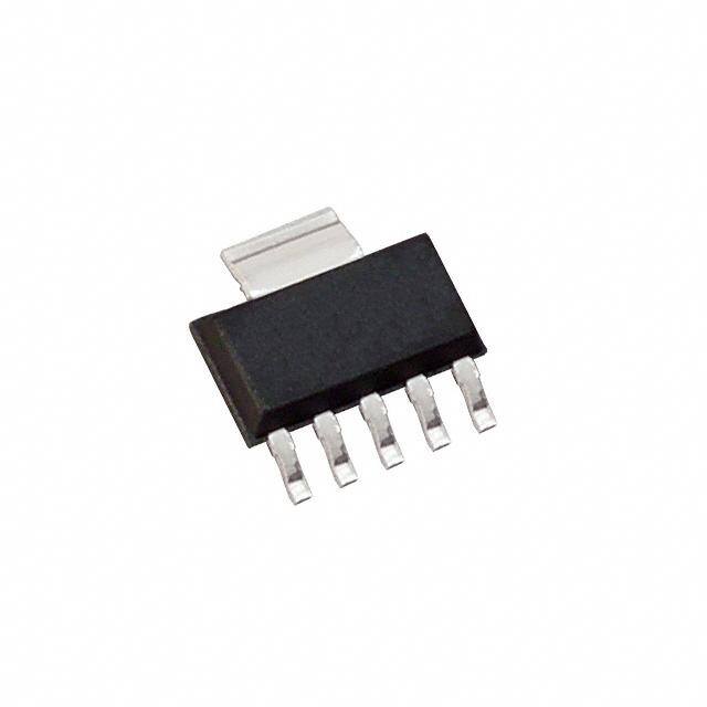
| 描述 | IC REG LDO 1.6V 0.5A SOT223-6低压差稳压器 High PSRR Fast RF High-Enable 500mA |
| 产品分类 | |
| 品牌 | Texas Instruments |
| 产品手册 | |
| 产品图片 |
|
| rohs | 符合RoHS无铅 / 符合限制有害物质指令(RoHS)规范要求 |
| 产品系列 | 电源管理 IC,低压差稳压器,Texas Instruments TPS79516DCQ- |
| 数据手册 | |
| 产品型号 | TPS79516DCQ |
| 产品种类 | 低压差稳压器 |
| 供应商器件封装 | SOT-223-6 |
| 其它名称 | 296-34654-5 |
| 包装 | 管件 |
| 单位重量 | 121 mg |
| 商标 | Texas Instruments |
| 安装类型 | 表面贴装 |
| 安装风格 | SMD/SMT |
| 封装 | Tube |
| 封装/外壳 | SOT-223-6 |
| 封装/箱体 | SOT-223-6 |
| 工作温度 | -40°C ~ 125°C |
| 工厂包装数量 | 78 |
| 最大工作温度 | + 125 C |
| 最大输入电压 | 5.5 V |
| 最小工作温度 | - 40 C |
| 最小输入电压 | + 2.7 V |
| 标准包装 | 78 |
| 电压-跌落(典型值) | - |
| 电压-输入 | 2.7 V ~ 5.5 V |
| 电压-输出 | 1.6V |
| 电压调节准确度 | 2 % |
| 电流-输出 | 500mA |
| 电流-限制(最小值) | 2.4A |
| 稳压器拓扑 | 正,固定式 |
| 稳压器数 | 1 |
| 系列 | TPS79516 |
| 线路调整率 | 0.05 % / V |
| 负载调节 | 3 mV |
| 输入偏压电流—最大 | 0.265 mA |
| 输出电压 | 1.6 V |
| 输出电流 | 500 mA |
| 输出端数量 | 1 Output |
| 输出类型 | Fixed |
| 配用 | /product-detail/zh/TPS78633EVM-207/296-20625-ND/562085 |


- 商务部:美国ITC正式对集成电路等产品启动337调查
- 曝三星4nm工艺存在良率问题 高通将骁龙8 Gen1或转产台积电
- 太阳诱电将投资9.5亿元在常州建新厂生产MLCC 预计2023年完工
- 英特尔发布欧洲新工厂建设计划 深化IDM 2.0 战略
- 台积电先进制程称霸业界 有大客户加持明年业绩稳了
- 达到5530亿美元!SIA预计今年全球半导体销售额将创下新高
- 英特尔拟将自动驾驶子公司Mobileye上市 估值或超500亿美元
- 三星加码芯片和SET,合并消费电子和移动部门,撤换高东真等 CEO
- 三星电子宣布重大人事变动 还合并消费电子和移动部门
- 海关总署:前11个月进口集成电路产品价值2.52万亿元 增长14.8%


PDF Datasheet 数据手册内容提取
Product Order Technical Tools & Support & Folder Now Documents Software Community TPS795 SLVS350J–OCTOBER2002–REVISEDMAY2019 TPS795 Ultralow-Noise, High-PSRR, Fast, RF, 500-mA, Low-Dropout Linear Regulators 1 Features 3 Description • 500-mAlow-dropoutregulatorwithenable The TPS795 family of low-dropout (LDO), low-power 1 linear voltage regulators features high power-supply • Availableinfixedandadjustable(1.2-Vto5.5-V) rejection ratio (PSRR), ultralow noise, fast start-up, versions and excellent line and load transient responses in • HighPSRR(50dBat10kHz) small outline, 6-pin SOT-223 and 3-mm × 3-mm • Ultralownoise(33µV ,TPS79530) VSON packages. Each device in the family is stable RMS with a small 1-µF ceramic capacitor on the output. • Faststart-uptime(50µs) The family uses an advanced, proprietary BiCMOS • Stablewitha1-µFceramiccapacitor fabrication process to yield extremely low dropout • Excellentloadandlinetransientresponse voltages (for example, 110 mV at 500 mA). Each device achieves fast start-up times (approximately • Lowdropoutvoltage(110mVatfullload, 50 µs with a 0.001-µF bypass capacitor) while TPS79530) consuming very low quiescent current (265 µA, • 6-pinSOT-223and3-mm×3-mmVSON typical). Moreover, when the device is placed in packages standby mode, the supply current is reduced to less than 1 µA. The TPS79530 device exhibits 2 Applications approximately 33 µV of output voltage noise at 3- RMS V output with a 0.1-µF bypass capacitor. Applications • RF:VCOs,receivers,ADCs with analog components that are noise-sensitive, • Audio such as portable RF electronics, benefit from the • Bluetooth®,wirelessLAN high-PSRR and low-noise features, as well as from thefastresponsetime. • Cellularandcordlesstelephones • Handheldorganizers,PDAs DeviceInformation(1) PARTNUMBER PACKAGE BODYSIZE(NOM) SOT-223(6) 6.50mm×3.50mm TPS795 VSON(8) 3.00mm×3.00mm (1) Forallavailablepackages,seethepackageoptionaddendum attheendofthedatasheet. TPS79530RippleRejectionvsFrequency TPS79530vsFrequency 80 0.5 VIN= 4 V Hz VIN= 5.5 V −dB 6700 CCNORUT== 0 1.001mmFF IOUT= 1 mA ÖV/sity−m 0.4 CCONRUT= =0 .21.m2FmF Ripple Rejection 345000 IOUT= 500 mA ectral Noise Den 00..23 IOUT= 1 mA 20 Sp IOUT= 0.5A ut 0.1 10 utp O 0 0 1 10 100 1 k 10 k 100 k 1 M 10 M 100 1 k 10 k 100 k Frequency(Hz) Frequency (Hz) 1 An IMPORTANT NOTICE at the end of this data sheet addresses availability, warranty, changes, use in safety-critical applications, intellectualpropertymattersandotherimportantdisclaimers.PRODUCTIONDATA.
TPS795 SLVS350J–OCTOBER2002–REVISEDMAY2019 www.ti.com Table of Contents 1 Features.................................................................. 1 8 ApplicationandImplementation........................ 13 2 Applications........................................................... 1 8.1 ApplicationInformation............................................13 3 Description............................................................. 1 8.2 TypicalApplication..................................................13 4 RevisionHistory..................................................... 2 8.3 WhattoDoandWhatNottoDo.............................15 5 PinConfigurationandFunctions......................... 3 9 PowerSupplyRecommendations...................... 16 6 Specifications......................................................... 3 10 Layout................................................................... 16 6.1 AbsoluteMaximumRatings......................................3 10.1 LayoutGuidelines.................................................16 6.2 ESDRatings..............................................................3 10.2 LayoutExamples...................................................19 6.3 RecommendedOperatingConditions.......................4 11 DeviceandDocumentationSupport................. 21 6.4 ThermalInformation..................................................4 11.1 DeviceSupport......................................................21 6.5 ElectricalCharacteristics...........................................5 11.2 DocumentationSupport........................................21 6.6 TypicalCharacteristics..............................................6 11.3 ReceivingNotificationofDocumentationUpdates21 7 DetailedDescription............................................ 10 11.4 CommunityResources..........................................21 7.1 Overview.................................................................10 11.5 Trademarks...........................................................22 7.2 FunctionalBlockDiagrams.....................................10 11.6 ElectrostaticDischargeCaution............................22 7.3 FeatureDescription.................................................11 11.7 Glossary................................................................22 7.4 DeviceFunctionalModes........................................12 12 Mechanical,Packaging,andOrderable Information........................................................... 22 4 Revision History NOTE:Pagenumbersforpreviousrevisionsmaydifferfrompagenumbersinthecurrentversion. ChangesfromRevisionI(May2015)toRevisionJ Page • ChangedDRBpackagenamethroughoutdatasheetfromSONtoVSON........................................................................... 1 • ChangedPinConfigurationpackagenames;switcheddesignatorstomatchcorrectpackagenames(typo) .....................3 • Addednote(1)toRecommendedOperatingConditions;movedfromElectricalCharacteristics.......................................... 4 • ChangedthermalvaluesinThermalInformationtable........................................................................................................... 4 • DeletedInputVoltagefromElectricalCharacteristics;alreadyshowninRecommendedOperatingConditions...................5 • DeletedJunctionTemperaturefromElectricalCharacteristics;alreadyshowninRecommendedOperatingConditions.....5 ChangesfromRevisionH(August2010)toRevisionI Page • AddedESDRatingstable,FeatureDescriptionsection,DeviceFunctionalModes,ApplicationandImplementation section,PowerSupplyRecommendationssection,Layoutsection,DeviceandDocumentationSupportsection,and Mechanical,Packaging,andOrderableInformationsection ................................................................................................. 1 • Changedfront-pagegraphic .................................................................................................................................................. 1 • ChangedPinConfigurationandFunctionssection;updatedtableformatandaddedpinoutdrawings................................. 3 • Changed"free-air"to"junction"temperatureinconditionstatementforAbsoluteMaximumRatings .................................. 3 • AddedAddedOperatingjunctiontemperaturespecificationtoElectricalCharacteristics..................................................... 5 • DeletedStart-uptimesymbol................................................................................................................................................. 5 • CorrectedminvalueforI parameter............................................................................................................................... 5 EN(HI) • AddedThermalshutdowntemperaturespecificationtoElectricalCharacteristics................................................................ 5 • AddedconditionstatementtoTypicalCharacteristicssection .............................................................................................. 6 • ChangedtitleforThermalProtectionsection ...................................................................................................................... 16 ChangesfromRevisionG(July,2006)toRevisionH Page • ReplacedtheDissipationRatingstablewiththeThermalInformationtable.......................................................................... 4 • UpdatedtheThermalProtectionsection.............................................................................................................................. 16 2 SubmitDocumentationFeedback Copyright©2002–2019,TexasInstrumentsIncorporated ProductFolderLinks:TPS795
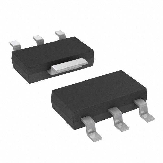
TPS795 www.ti.com SLVS350J–OCTOBER2002–REVISEDMAY2019 5 Pin Configuration and Functions DRBPackage DCQPackage 8-PinVSON 6-PinSOT-223 TopView TopView IN 1 8 EN 6 IN 2 7 N/C OUT 3 6 GND OUT 4 5 NR/FB 1 2 3 4 5 EN GND NR/FB IN OUT PinFunctions PIN I/O DESCRIPTION NAME VSON SOT-223 IN 1,2 2 I Unregulatedinputtothedevice GND 6 3,6 — Regulatorground Drivingtheenablepin(EN)highturnsontheregulator.Drivingthispinlowputsthe EN 8 1 I regulatorintoshutdownmode.ENcanbeconnectedtoINifnotused. Noise-reductionpinforfixedversionsonly.Connectinganexternalcapacitortothispin NR 5 5 — bypassesnoisegeneratedbytheinternalbandgap,whichimprovespower-supply rejectionandreducesoutputnoise.(Notavailableonadjustableversions.) Feedbackinputvoltagefortheadjustabledevice. FB 5 5 I (Notavailableonfixedvoltageversions.) OUT 3,4 4 O Regulatoroutput N/C 7 – — Nointernalconnection 6 Specifications 6.1 Absolute Maximum Ratings overoperatingjunctiontemperaturerange(unlessotherwisenoted)(1) MIN MAX UNIT IN –0.3 6 Voltage EN –0.3 V +0.3 V IN OUT 6 Current Peakoutput Internallylimited A Powerdissipation Continuoustotal SeeThermalInformation Junction,T –40 150 °C J Temperature Storage,T –65 150 °C stg (1) StressesbeyondthoselistedunderAbsoluteMaximumRatingsmaycausepermanentdamagetothedevice.Thesearestressratings only,whichdonotimplyfunctionaloperationofthedeviceattheseoranyotherconditionsbeyondthoseindicatedunderRecommended OperatingConditions.Exposuretoabsolute-maximum-ratedconditionsforextendedperiodsmayaffectdevicereliability. 6.2 ESD Ratings VALUE UNIT Electrostatic Humanbodymodel(HBM),perANSI/ESDA/JEDECJS-001,allpins(1) ±2000 V V (ESD) discharge Chargeddevicemodel(CDM),perJEDECspecificationJESD22-C101,allpins(2) ±500 (1) JEDECdocumentJEP155statesthat500-VHBMallowssafemanufacturingwithastandardESDcontrolprocess. (2) JEDECdocumentJEP157statesthat250-VCDMallowssafemanufacturingwithastandardESDcontrolprocess. Copyright©2002–2019,TexasInstrumentsIncorporated SubmitDocumentationFeedback 3 ProductFolderLinks:TPS795
TPS795 SLVS350J–OCTOBER2002–REVISEDMAY2019 www.ti.com 6.3 Recommended Operating Conditions overoperatingjunctiontemperaturerange(unlessotherwisenoted) MIN NOM MAX UNIT V Inputvoltage(1) 2.7 5.5 V IN I Outputcurrent 0 500 mA OUT T Operatingjunctiontemperature –40 125 °C J (1) MinimumV is2.7VorV +V ,whicheverisgreater. IN OUT DO 6.4 Thermal Information overoperatingfree-airtemperaturerange(unlessotherwisenoted) TPS795(3) THERMALMETRIC(1)(2) DRB(VSON) DCQ(SOT-223) UNIT 6PINS 8PINS R Junction-to-ambientthermalresistance 46.8 74.0 °C/W θJA R Junction-to-case(top)thermalresistance 45.1 44.5 °C/W θJC(top) R Junction-to-boardthermalresistance 18.4 8.6 °C/W θJB ψ Junction-to-topcharacterizationparameter 0.7 3.2 °C/W JT ψ Junction-to-boardcharacterizationparameter 18.4 8.5 °C/W JB R Junction-to-case(bottom)thermalresistance 5.3 N/A °C/W θJC(bot) (1) Formoreinformationabouttraditionalandnewthermalmetrics,seetheSemiconductorandICPackageThermalMetricsapplication report. (2) ForthermalestimatesofthisdevicebasedonPCBcopperarea,seetheTIPCBThermalCalculator. (3) ThermaldatafortheDRBandDCQpackagesarederivedbythermalsimulationsbasedonJEDEC-standardmethodologyasspecified intheJESD51series.Thefollowingassumptionsareusedinthesimulations: (a)i. DRB: The exposed pad is connected to the PCB ground layer through a 2-mm x 2-mm thermal via array. .ii.DCQ:TheexposedpadisconnectedtothePCBgroundlayerthrougha3-mmx2-mmthermalviaarray. (b)i.DRB: The topandbottomcopper layers areassumed to have a 20% thermal conductivity of copper representing a 20% copper coverage. .ii.DCQ:Eachoftopandbottomcopperlayershasadedicatedpatternfor20%coppercoverage. (c)ThesedataweregeneratedwithonlyasingledeviceatthecenterofaJEDEChigh-K(2s2p)boardwith3in×3incopperarea.To understandtheeffectsofthecopperareaonthermalperformance,seeThermalConsiderationsandEstimatingJunctionTemperature ofthisdatasheet. 4 SubmitDocumentationFeedback Copyright©2002–2019,TexasInstrumentsIncorporated ProductFolderLinks:TPS795
TPS795 www.ti.com SLVS350J–OCTOBER2002–REVISEDMAY2019 6.5 Electrical Characteristics overrecommendedoperatingtemperaturerange(T =–40°Cto125°C),V =V ,V =V +1V(1),I =1mA,C J EN IN IN OUT(nom) OUT OUT =10µF,andC =0.01µF(unlessotherwisenoted);typicalvaluesareat25°C NR PARAMETER TESTCONDITIONS MIN TYP MAX UNIT VFB Internalreference(TPS79501) 1.200 1.225 1.25 V Outputvoltagerange TPS79501 1.225 5.5–VDO V TPS79501(2) 0VOµUAT(≤nomIO)U+T1≤V50≤0VmINA≤,5.5V(1) 0.98VOUT(nom) VOUT(nom) 1.02VOUT(nom) V Accuracy FixedVOUT<5V 0VOµUAT(≤nomIO)U+T1≤V50≤0VmINA≤,5.5V(1) –2% 2% ΔVO(ΔVI) Lineregulation(1) VOUT+1V≤VIN≤5.5V 0.05 0.12 %/V ΔVO(ΔIO) Loadregulation 0µA≤IOUT≤500mA 3 mV Dropoutvoltage(3) TPS79530 IOUT=500mA 110 170 mV VDO (VIN=VOUT(nom)–0.1V) TPS79533 IOUT=500mA 105 160 mV ICL Outputcurrentlimit VOUT=0V 2.4 2.8 4.2 A IGND Groundpincurrent 0µA≤IOUT≤500mA 265 385 µA ISHDN Shutdowncurrent(4) VEN=0V,2.7V≤VIN≤5.5V 0.07 1 µA IFB Feedbackpincurrent VFB=1.225V 1 µA f=100Hz,IOUT=10mA 59 dB f=100Hz,IOUT=500mA 58 dB PSRR Power-supplyrejectionratio(TPS79530) f=10kHz,IOUT=500mA 50 dB f=100kHz,IOUT=500mA 39 dB CNR=0.001µF 46 µVRMS BW=100Hzto CNR=0.0047µF 41 µVRMS Vn Outputnoisevoltage(TPS79530) 100kHz, IOUT=500mA CNR=0.01µF 35 µVRMS CNR=0.1µF 33 µVRMS CNR=0.001µF 50 µs Start-uptime(TPS79530) RL=6Ω,COUT=1µF CNR=0.0047µF 75 µs CNR=0.01µF 110 µs VEN(HI) Enablehigh(enabled) 2.7V≤VIN≤5.5V 1.7 VIN V VEN(LO) Enablelow(shutdown) 2.7V≤VIN≤5.5V 0.7 V IEN(HI) Enablepincurrent,enabled VEN=0V –1 1 µA UVLO Undervoltagelockout VCCrising 2.25 2.65 V UVLOhysteresis 100 mV Shutdown,temperatureincreasing 165 °C Tsd Thermalshutdowntemperature Reset,temperaturedecreasing 140 °C (1) MinimumV is2.7VorV +V ,whicheverisgreater. IN OUT DO (2) Toleranceofexternalresistorsnotincludedinthisspecification. (3) DropoutisnotmeasuredfortheTPS79501andTPS79525becauseminimumV =2.7V. IN (4) Foradjustableversion,thisappliesonlyafterV isapplied;thenV transitionshightolow. IN EN Copyright©2002–2019,TexasInstrumentsIncorporated SubmitDocumentationFeedback 5 ProductFolderLinks:TPS795
TPS795 SLVS350J–OCTOBER2002–REVISEDMAY2019 www.ti.com 6.6 Typical Characteristics atV =V ,V =V +1V,I =1mA,C =10µF,C =0.01µF,C =2.2µF,andT =25°C(unlessotherwise EN IN IN OUT(nom) OUT OUT NR IN J noted) 3.02 3.005 VIN=4V 3 COUT=10mF 3.01 2.995 IOUT=1mA V) 2.99 V(OUT 3 (V)UT 2.985 IOUT=0.5A O V 2.99 2.98 2.975 2.98 2.97 0 0.1 0.2 0.3 0.4 0.5 −40−25−105 20 35 50 65 80 95 110125 IOUT(mA) TJ(°C) Figure1.TPS79530OutputVoltagevsOutputCurrent Figure2.TPS79530OutputVoltagevsJunction Temperature 276 0.5 274 VCIONU=T4=V10mF √HV/zm 0.4 VCCIONNRU=T=5=0.5.21.V2mFmF 272 − y 270 IOUT=1mA ensit 0.3 IOUT=1mA I(A)mGND 226668 IOUT=0.5A ctral Noise D 0.2 226624 put Spe 0.1 IOUT=0.5A ut O 260 0 −40−25−105 20 35 50 65 80 95110125 100 1k 10k 100k TJ(°C) Frequency (Hz) Figure3.TPS79530GroundCurrentvsJunction Figure4.TPS79530OutputSpectralNoiseDensityvs Temperature Frequency 0.6 2.5 √V/Hzm 0.5 VCCIONNRU=T=5=0.5.110VmmFF √V/Hzm 2 VICOIONUUT=T==55.15000VmmFA Spectral Noise Density− 000...234 IOUT=IO0U.5TA=1mA pectral Noise Density− 1.51 CNR=0.00C1NCmRNFCR=N=0R.00=0.04017.1mmmFFF put 0.1 utS 0.5 Out utp 0 O 100 1k 10k 100k 0100 1k 10k 100k Frequency (Hz) Frequency (Hz) Figure5.TPS79530OutputSpectralNoiseDensityvs Figure6.TPS79530OutputSpectralNoiseDensityvs Frequency Frequency 6 SubmitDocumentationFeedback Copyright©2002–2019,TexasInstrumentsIncorporated ProductFolderLinks:TPS795
TPS795 www.ti.com SLVS350J–OCTOBER2002–REVISEDMAY2019 Typical Characteristics (continued) atV =V ,V =V +1V,I =1mA,C =10µF,C =0.01µF,C =2.2µF,andT =25°C(unlessotherwise EN IN IN OUT(nom) OUT OUT NR IN J noted) S 50 175 Ve−mRM 40 ICOOUUTT==51000mmFA 150 VCIOIONUUT=T=2=5.91000VmmFA s Noi 125 ut p 30 uared Out 20 V(mV)DO 10705 q S n 50 a Me 10 ot 25 o R BW=100Hzto100kHz RMS− 00.001 0.0047 0.01 0.1 0−40−25−10 5 20 35 50 65 80 95110125 CNR(mF) TJ(°C) Figure7.TPS79530RootMeanSquaredOutputNoisevs Figure8.TPS79530DropoutVoltagevsJunction C Temperature NR 80 80 VIN=4V VIN=4V 70 COUT=10mF 70 COUT=10mF dB 60 CNR=0.1mF IOUT=1mA dB 60 CNR=0.01mF IOUT=1mA − − Ripple Rejection 23450000 IOUT=500mA Ripple Rejection 23450000 IOUT=500mA 10 10 0 0 1 10 100 1k 10k 100k 1M 10M 1 10 100 1k 10k 100k 1M 10M Frequency (Hz) Frequency (Hz) Figure9.TPS79530RippleRejectionvsFrequency Figure10.TPS79530RippleRejectionvsFrequency 80 80 VIN=4V VIN=4V 70 COUT=2.2mF 70 COUT=2.2mF CNR=0.01mF CNR=0.1mF dB 60 IOUT=1mA dB 60 IOUT=1mA − − on 50 on 50 cti cti eje 40 eje 40 R R e e pl 30 pl 30 Rip IOUT=500mA Rip IOUT=500mA 20 20 10 10 0 0 1 10 100 1k 10k 100k 1M 10M 1 10 100 1k 10k 100k 1M 10M Frequency (Hz) Frequency (Hz) Figure11.TPS79530RippleRejectionvsFrequency Figure12.TPS79530RippleRejectionvsFrequency Copyright©2002–2019,TexasInstrumentsIncorporated SubmitDocumentationFeedback 7 ProductFolderLinks:TPS795
TPS795 SLVS350J–OCTOBER2002–REVISEDMAY2019 www.ti.com Typical Characteristics (continued) atV =V ,V =V +1V,I =1mA,C =10µF,C =0.01µF,C =2.2µF,andT =25°C(unlessotherwise EN IN IN OUT(nom) OUT OUT NR IN J noted) 3 20 2.75 CNR=0.001mF 2.50 CNR=0.0047mF mV)10 2.252 CNR=0.01mF (OUT 0 Enable V 1.75 −10 (V) 1.50 N VI 1.25 −20 COUT=10mF,CNR=0.01mF, 1 IOUT=0.5A,dv/dt=1V/ms 4 0.75 00..2550 VCIOIONUUT=T=4=0V1.50AmF V(V)IN 3 0 2 0 100 200 300 400 500 600 0 50 100 150 200 t (ms) t (ms) Figure13.TPS79530Start-UpTime Figure14.TPS79518LineTransientResponse 30 60 20 mV) 40 ( mV) 10 VOUT 20 (T 0 OU 0 V −20 −10 −40 V(V)IN−2450 CIOOUUTT==01.50Am,F,dCv/NdRt==10V.0/1msmF, I(A)OUT−06.500 CVLOU=T3=.81V0,mdFv,/dCtN=R0=.50A.0/m1smF, 3 −0.5 0 200 400 600 800 1000 0 50 100 150 200 t (ms) t (ms) Figure15.TPS79530LineTransientResponse Figure16.TPS79530LoadTransientResponse 4.5 180 4 VROLU=T1=02W.5V, 160 3.5 140 VIN TJ=125°C 3 120 2.5 TJ=25°C (V)T 2 mV) 100 VOU 1.5 (DO 80 V 1 VOUT 60 TJ=−40°C 0.5 40 0 20 −0.5 0 0 400 800 1200 1600 2000 0 100 200 300 400 500 Time (ms) IOUT(mA) Figure17.TPS79525PowerUpandPowerDown Figure18.TPS79530DropoutVoltagevsOutputCurrent 8 SubmitDocumentationFeedback Copyright©2002–2019,TexasInstrumentsIncorporated ProductFolderLinks:TPS795
TPS795 www.ti.com SLVS350J–OCTOBER2002–REVISEDMAY2019 Typical Characteristics (continued) atV =V ,V =V +1V,I =1mA,C =10µF,C =0.01µF,C =2.2µF,andT =25°C(unlessotherwise EN IN IN OUT(nom) OUT OUT NR IN J noted) 200 100 COUT=10mF, COUT=1mF CNR=0.01mF, IOUT=50mA Regionof 150 10 Instability TJ=125°C )Ω ( mV) 100 TJ=25°C ESR 1 ( O D V RegionofStability 50 TJ=−40°C 0.1 0 0.01 2.5 3 3.5 4 4.5 5 0 100 200 300 400 500 VIN(V) IOUT(mA) Figure19.TPS79501DropoutVoltagevsInputVoltage Figure20.TPS79530TypicalRegionsofStabilityEquivalent SeriesResistance(ESR)vsOutputCurrent 100 100 COUT=2.2mF Regionof COUT=10mF Instability 10 10 Regionof Instability )Ω )Ω SR( 1 SR( 1 E E 0.1 RegionofStability 0.1 RegionofStability 0.01 0.01 1 10 100 1000 0 100 200 300 400 500 IOUT(mA) IOUT(A) Figure21.TPS79530TypicalRegionsofStabilityEquivalent Figure22.TPS79530TypicalRegionsofStabilityEquivalent SeriesResistance(ESR)vsOutputCurrent SeriesResistance(ESR)vsOutputCurrent Copyright©2002–2019,TexasInstrumentsIncorporated SubmitDocumentationFeedback 9 ProductFolderLinks:TPS795
TPS795 SLVS350J–OCTOBER2002–REVISEDMAY2019 www.ti.com 7 Detailed Description 7.1 Overview The TPS795 family of LDO regulators combines the high performance required of many RF and precision analog applications with low current consumption. High PSRR is provided by a high-gain, high-bandwidth error loop with good supply rejection at very low headroom (V – V ). A noise-reduction pin is provided to bypass noise IN OUT generated by the band-gap reference and to improve PSRR, while a quick-start circuit quickly charges this capacitor at start-up. All versions have thermal and overcurrent protection, and are fully specified from –40°C to +125°C. 7.2 Functional Block Diagrams IN OUT 300W UVLO Current Sense Overshoot Detect GND ILIM SHUTDOWN R 1 EN FB UVLO Thermal R 2 Shutdown Quickstart Externalto theDevice Bandgap V V Reference REF IN 1.225V 250kW Figure23. FunctionalBlockDiagram—AdjustableVersion IN OUT 300W UVLO Current Sense Overshoot Detect GND ILIM SHUTDOWN R 1 EN UVLO Thermal R 2 Shutdown Quickstart R2=40kW Bandgap V V Reference REF NR IN 1.225V 250kW Figure24. FunctionalBlockDiagram—FixedVersions 10 SubmitDocumentationFeedback Copyright©2002–2019,TexasInstrumentsIncorporated ProductFolderLinks:TPS795
TPS795 www.ti.com SLVS350J–OCTOBER2002–REVISEDMAY2019 7.3 Feature Description 7.3.1 Shutdown The enable pin (EN) is active high and is compatible with standard and low-voltage TTL-CMOS levels. When shutdowncapabilityisnotrequired,ENcanbeconnectedtoIN. 7.3.2 Start-Up The TPS795 uses a start-up circuit to quickly charge the noise reduction capacitor, C , if present (see NR Functional Block Diagrams). This circuit allows for the combination of very low output noise and fast start-up times. The NR pin is high impedance so a low leakage C capacitor must be used; most ceramic capacitors are NR appropriateforthisconfiguration. For the fastest start-up, apply V first, and then drive the enable pin (EN) high. If EN is tied to IN, start-up is IN somewhatslower.ToensurethatC isfullychargedduringstart-up,usea0.1-µForsmallercapacitor. NR 7.3.3 UndervoltageLockout(UVLO) The TPS795 uses an undervoltage lockout circuit to keep the output shut off until internal circuitry is operating properly. The UVLO circuit has approximately 100 mV of hysteresis to help reject input voltage drops when the regulatorfirstturnson. 7.3.4 RegulatorProtection The TPS795 PMOS-pass transistor has a built-in back diode that conducts reverse current when the input voltage drops below the output voltage (for example, during power down). Current is conducted from the output to the input and is not internally limited. If extended reverse voltage operation is anticipated, external limiting mightbeappropriate. The TPS795 features internal current limiting and thermal protection. During normal operation, the TPS795 limits outputcurrenttoapproximately2.8A.Whencurrentlimitingengages,theoutputvoltagescalesback linearly until the overcurrent condition ends. While current limiting is designed to prevent gross device failure, care should be taken not to exceed the power dissipation ratings of the package. If the temperature of the device exceeds approximately 165°C (T ), thermal-protection circuitry shuts it down. Once the device has cooled down to less sd thanapproximately140°C,regulatoroperationresumes. Copyright©2002–2019,TexasInstrumentsIncorporated SubmitDocumentationFeedback 11 ProductFolderLinks:TPS795
TPS795 SLVS350J–OCTOBER2002–REVISEDMAY2019 www.ti.com 7.4 Device Functional Modes Table1providesaquickcomparisonbetweenthenormal,dropout,anddisabledmodesofoperation. Table1.DeviceFunctionalModeComparison PARAMETER OPERATINGMODE V EN I T IN OUT J Normal V >V +V V >V I <I T <T IN OUT(nom) DO EN EN(HI) OUT CL J sd Dropout V <V +V V >V I <I T <T IN OUT(nom) DO EN EN(HI) OUT CL J sd Disabled — V <V — T >T EN EN(LO) J sd 7.4.1 NormalOperation Thedeviceregulatestothenominaloutputvoltageunderthefollowingconditions: • Theinputvoltageisgreaterthanthenominaloutputvoltageplusthedropoutvoltage(V +V ). OUT(nom) DO • The enable voltage has previously exceeded the enable rising threshold voltage and not yet decreased below theenablefallingthreshold. • Theoutputcurrentislessthanthecurrentlimit(I <I ). OUT CL • Thedevicejunctiontemperatureislessthanthethermalshutdowntemperature(T <T ). J sd 7.4.2 DropoutOperation If the input voltage is lower than the nominal output voltage plus the specified dropout voltage, but all other conditions are met for normal operation, the device operates in dropout mode. In this mode, the output voltage tracks the input voltage. During this mode, the transient performance of the device becomes significantly degraded because the pass device is in the linear region and no longer controls the current through the LDO. Lineorloadtransientsindropoutcanresultinlargeoutput-voltagedeviations. 7.4.3 Disabled Thedeviceisdisabledunderthefollowingconditions: • The enable voltage is less than the enable falling threshold voltage or has not yet exceeded the enable rising threshold. • Thedevicejunctiontemperatureisgreaterthanthethermalshutdowntemperature(T >T ). J sd 12 SubmitDocumentationFeedback Copyright©2002–2019,TexasInstrumentsIncorporated ProductFolderLinks:TPS795
TPS795 www.ti.com SLVS350J–OCTOBER2002–REVISEDMAY2019 8 Application and Implementation NOTE Information in the following applications sections is not part of the TI component specification, and TI does not warrant its accuracy or completeness. TI’s customers are responsible for determining suitability of components for their purposes. Customers should validateandtesttheirdesignimplementationtoconfirmsystemfunctionality. 8.1 Application Information The TPS795 family of LDO regulators has been optimized for use in noise-sensitive equipment. The device features extremely low dropout voltages, high PSRR, ultralow output noise, low quiescent current (265 µA, typically),andanenableinputtoreducesupplycurrentstolessthan1 µAwhentheregulatoristurnedoff. 8.2 Typical Application AtypicalapplicationcircuitisshowninFigure25. VIN IN OUT VOUT TPS795xx 1mF EN GND NR 1mF 0.01mF Figure25. TypicalApplicationCircuit 8.2.1 DesignRequirements Table2liststhedesignrequirements. Table2.DesignParameters PARAMETER DESIGNREQUIREMENT Inputvoltage 3.3V Outputvoltage 2.5V Maximumoutputcurrent 500mA 8.2.2 DetailedDesignProcedure Selectthedesireddevicebasedontheoutputvoltage. Provide an input supply with adequate headroom to account for dropout and output current to account for the GNDterminalcurrent,andpowertheload. 8.2.2.1 InputandOutputCapacitorRequirements Although not required, it is good analog design practice to place a 0.1-µF to 2.2-µF capacitor near the input of the regulator to counteract reactive input sources. A higher-value input capacitor may be necessary if large, fast- risetimeloadtransientsareanticipatedandthedeviceislocatedseveralinchesfromthepowersource. Like most low dropout regulators, the TPS795 requires an output capacitor connected between OUT and GND to stabilize the internal control loop. The minimum recommended capacitor is 1 µF. Any 1-µF or larger ceramic capacitorissuitable. Copyright©2002–2019,TexasInstrumentsIncorporated SubmitDocumentationFeedback 13 ProductFolderLinks:TPS795
TPS795 SLVS350J–OCTOBER2002–REVISEDMAY2019 www.ti.com 8.2.2.2 OutputNoise The internal voltage reference is a key source of noise in an LDO regulator. The TPS795 has an NR pin which is connected to the voltage reference through a 250-kΩ internal resistor. The 250-kΩ internal resistor, in conjunction with an external bypass capacitor connected to the NR pin, creates a low-pass filter to reduce the voltage reference noise and, therefore, the noise at the regulator output. For the regulator to operate properly, thecurrentflowoutoftheNRpinmustbeataminimum,because any leakage current creates an IR drop across the internal resistor, thus creating an output error. Therefore, the bypass capacitor must have minimal leakage current. The bypass capacitor should be no more than 0.1 µF to ensure that it is fully charged during the quickstarttimeprovidedbytheinternalswitchshowninFunctionalBlockDiagrams. For example, the TPS79530 exhibits 40 µV of output voltage noise using a 0.1-µF ceramic bypass capacitor RMS and a 10-µF ceramic output capacitor. The output starts up slower as the bypass capacitance increases due to theRCtimeconstantatthebypasspinthatiscreatedbytheinternal250-kΩresistorandexternalcapacitor. 8.2.2.3 DropoutVoltage The TPS795 uses a PMOS pass transistor to achieve a low dropout voltage. When (V – V ) is less than the IN OUT dropout voltage (V ), the PMOS pass device is in its linear region of operation and r of the PMOS pass DO DS(on) element is the input-to-output resistance. Because the PMOS device behaves like a resistor in dropout, V DO approximatelyscaleswiththeoutputcurrent. As with any linear regulator, PSRR degrades as (V – V ) approaches dropout. This effect is illustrated in IN OUT Figure9 throughFigure12. 8.2.2.4 ProgrammingtheTPS79501AdjustableLDORegulator The output voltage of the TPS79501 adjustable regulator is programmed using an external resistor divider as showninFigure26. VIN IN OUT VOUT PROOUGTRPAUMTMVIONLGT AGGUEIDE TPS79501 1μF EN R1 C1 1μF OUTPUT GND FB VOLTAGE R1 R2 C1 R2 1.8 V 14.0 kΩ 30.1 kΩ 33 pF 3.6 V 57.9 kΩ 30.1 kΩ 15 pF Figure26. TypicalApplication,AdjustableOutput TheoutputvoltageiscalculatedusingEquation1. § R • V V u¤1(cid:14) 1‚ OUT REF ' R „ 2 where • V =1.2246Vtypical(theinternalreferencevoltage) (1) REF Resistors R and R should be chosen for approximately 40-µA divider current. Lower value resistors can be 1 2 used for improved noise performance, but the device wastes more power. Higher values should be avoided, as leakagecurrentatFBincreasestheoutputvoltageerror. 14 SubmitDocumentationFeedback Copyright©2002–2019,TexasInstrumentsIncorporated ProductFolderLinks:TPS795
TPS795 www.ti.com SLVS350J–OCTOBER2002–REVISEDMAY2019 TherecommendeddesignprocedureistochooseR =30.1kΩtosetthedividercurrentat 40 µA, C = 15 pF for 2 1 stability,andthencalculateR usingEquation2. 1 §V • R ¤ OUT (cid:16)1‚uR 1 2 'V „ REF (2) To improve the stability of the adjustable version, TI suggests placing a small compensation capacitor between OUTandFB. TheapproximatevalueofthiscapacitorcanbecalculatedusingEquation3. (cid:11)3u10(cid:16)7(cid:12)u(cid:11)R (cid:14)R (cid:12) 1 2 C 1 (cid:11)R uR (cid:12) 1 2 (3) The suggested value of this capacitor for several resistor ratios is shown in the table within Figure 26. If this capacitor is not used (such as in a unity-gain configuration), then the minimum recommended output capacitor is 2.2 µFinsteadof1 µF. 8.2.3 ApplicationCurves 0.6 80 √V/Hz−m 0.5 VCCIONNRU=T=5=0.5.110VmmFF B 6700 VCCIONNRU=T=4=0V.110mmFF IOUT=1mA y d nsit 0.4 IOUT=1mA n− 50 e o Spectral Noise D 00..23 IOUT=0.5A Ripple Rejecti 234000 IOUT=500mA put 0.1 10 ut O 0 0 100 1k 10k 100k 1 10 100 1k 10k 100k 1M 10M Frequency (Hz) Frequency (Hz) Figure27.TPS79530OutputSpectralNoiseDensityvs Figure28.TPS79530RippleRejectionvsFrequency Frequency 8.3 What to Do and What Not to Do Placeatleastone1-µFceramiccapacitorascloseaspossibletotheOUTpinoftheregulator. Donotplacetheoutputcapacitormorethan10mmawayfromtheregulator. Connect a 0.1-µF or larger, low equivalent series resistance (ESR) capacitor across the IN pin and GND input of theregulator. Donotexceedtheabsolutemaximumratings. Copyright©2002–2019,TexasInstrumentsIncorporated SubmitDocumentationFeedback 15 ProductFolderLinks:TPS795
TPS795 SLVS350J–OCTOBER2002–REVISEDMAY2019 www.ti.com 9 Power Supply Recommendations These devices are designed to operate from an input voltage supply range from 2.7 V to 5.5 V. The input voltage range provides adequate headroom for the device to have a regulated output. This input supply is well-regulated and stable. If the input supply is noisy, additional input capacitors with low ESR can help improve the output noiseperformance. 10 Layout 10.1 Layout Guidelines 10.1.1 BoardLayoutRecommendationtoImprovePSRRandNoisePerformance To improve ac measurements like PSRR, output noise, and transient response, TI recommends designing the board with separate ground planes for V and V , with each ground plane connected only at the ground pin of IN OUT the device. In addition, the ground connection for the bypass capacitor should connect directly to the ground pin ofthedevice. 10.1.2 RegulatorMounting The tab of the 6-pin SOT-223 package is electrically connected to ground. For best thermal performance, solder the tab of the surface-mount version directly to a circuit-board copper area. Increasing the copper area improves heatdissipation. Solder pad footprint recommendations for the devices are presented in application report SBFA015, Solder Pad RecommendationsforSurface-MountDevices,availablefromtheTIwebsite(www.ti.com). 10.1.3 ThermalConsiderations Knowing the device power dissipation and proper sizing of the thermal plane that is connected to the tab or pad iscriticaltoavoidingthermalshutdownandensuringreliableoperation. Power dissipation of the device depends on input voltage and load conditions and can be calculated using Equation4: P (cid:11)V (cid:16)V (cid:12)uI D IN OUT OUT (4) Power dissipation can be minimized and greater efficiency can be achieved by using the lowest possible input voltagenecessarytoachievetherequiredoutputvoltageregulation. On the VSON (DRB) package, the primary conduction path for heat is through the exposed pad to the printed- circuit-board (PCB). The pad can be connected to ground or be left floating; however, it should be attached to an appropriate amount of copper PCB area to ensure the device does not overheat. On the SOT-223 (DCQ) package, the primary conduction path for heat is through the tab to the PCB. The tab should be connected to ground. The maximum junction-to-ambient thermal resistance depends on the maximum ambient temperature, maximum device junction temperature, and power dissipation of the device and can be calculated using Equation5: (cid:11)(cid:14)125qC(cid:16)T (cid:12) R A TJA P D (5) 16 SubmitDocumentationFeedback Copyright©2002–2019,TexasInstrumentsIncorporated ProductFolderLinks:TPS795
TPS795 www.ti.com SLVS350J–OCTOBER2002–REVISEDMAY2019 Layout Guidelines (continued) Knowing the maximum R , the minimum amount of PCB copper area needed for appropriate heatsinking can θJA beestimatedusingFigure29. 160 140 120 100 W) C/ 80 DCQ (° A qJ 60 DRB 40 20 0 0 2 4 6 8 10 Board CopperArea (in2) Note: θ valueatboardsizeof9in.2(thatis,3in.×3in.)isaJEDECstandard. JA Figure29. Θ vsBoardSize JA Figure29showsthevariationof θ asa function of ground plane copper area in the board. It is intended only as JA a guideline to demonstrate the effect of heat spreading in the ground plane and should not be used to estimate thethermalperformanceinrealapplicationenvironments. NOTE When the device is mounted on an application PCB, it is strongly recommended to use Ψ and Ψ ,asexplainedinEstimatingJunctionTemperature. JT JB 10.1.4 EstimatingJunctionTemperature Using the thermal metrics Ψ and Ψ , as shown in Thermal Information, the junction temperature can be JT JB estimated with corresponding formulas (given in Equation 6). For backwards compatibility, an older θ ,Top JC parameterisalsolisted. Y : T = T +Y ·P JT J T JT D Y : T = T +Y ·P JB J B JB D where • P isthepowerdissipationshownbyEquation5 D • T isthetemperatureatthecenter-topoftheICpackage T • T isthePCBtemperaturemeasured1mmawayfromtheICpackageonthePCBsurface(seeFigure31) (6) B NOTE Both T and T can be measured on actual application boards using a thermo-gun (an T B infraredthermometer). For more information about measuring T and T , see the application note SBVA025, Using New Thermal T B Metrics,availablefordownloadatwww.ti.com. Copyright©2002–2019,TexasInstrumentsIncorporated SubmitDocumentationFeedback 17 ProductFolderLinks:TPS795
TPS795 SLVS350J–OCTOBER2002–REVISEDMAY2019 www.ti.com Layout Guidelines (continued) As shown in Figure 30, the new thermal metrics (Ψ and Ψ ) have little dependency on board size. That is, JT JB using Ψ or Ψ with Equation 6 is a good way to estimate T by simply measuring T or T , regardless of the JT JB J T B applicationboardsize. 35 DRBYJT 30 25 W) C/ DRBYJB (° 20 B YJ d 15 n a YJT10 DCQYTB DCQYJT 5 0 0 1 2 3 4 5 6 7 8 9 10 Board CopperArea (in2) Figure30. Ψ andΨ vsBoardSize JT JB For a more detailed discussion of why TI does not recommend using θ to determine thermal characteristics, JC(top) seetheapplicationreportSBVA025,UsingNewThermalMetrics,availableatwww.ti.com. For further information, see the application report SPRA953, IC Package Thermal Metrics, also available on the TIwebsite. X T 1mm B TTonTop of IC Surface TT X T on PCB B 1mm (a) Example DRB (SON) Package Measurement (b) Example DCQ (SOT-223) Package Measurement Figure31. MeasuringPointforT andT T B 18 SubmitDocumentationFeedback Copyright©2002–2019,TexasInstrumentsIncorporated ProductFolderLinks:TPS795
TPS795 www.ti.com SLVS350J–OCTOBER2002–REVISEDMAY2019 10.2 Layout Examples GND PLANE CIN TPS79501DRB VIN IN 1 8 EN IN 2 7 N/C OUT 3 6 GND VOUT OUT 4 5 NR/FB R2 COUT GND PLANE R1 Figure32. TPS79501(AdjustableVoltageVersion)—LayoutExample Copyright©2002–2019,TexasInstrumentsIncorporated SubmitDocumentationFeedback 19 ProductFolderLinks:TPS795
TPS795 SLVS350J–OCTOBER2002–REVISEDMAY2019 www.ti.com Layout Examples (continued) GND PLANE CIN TPS795xxDRB VIN IN 1 8 EN IN 2 7 N/C OUT 3 6 GND VOUT OUT 4 5 NR/FB CNR COUT GND PLANE Figure33. TPS795(FixedVoltageVersions)—LayoutExample 20 SubmitDocumentationFeedback Copyright©2002–2019,TexasInstrumentsIncorporated ProductFolderLinks:TPS795
TPS795 www.ti.com SLVS350J–OCTOBER2002–REVISEDMAY2019 11 Device and Documentation Support 11.1 Device Support 11.1.1 DevelopmentSupport 11.1.1.1 EvaluationModules An evaluation module (EVM) is available to assist in the initial circuit performance evaluation using the TPS795. The TPS79501DRBEVM evaluation module related (and user's guide) can be requested at the TI website throughtheproductfoldersorpurchaseddirectlyfromtheTIeStore. 11.1.1.2 SpiceModels Computer simulation of circuit performance using SPICE is often useful when analyzing the performance of analog circuits and systems. A SPICE model for the TPS795 is available through the product folders under Tools &Software. 11.1.2 DeviceNomenclature Table3. DeviceNomenclature(1) PRODUCT V OUT TPS795xx(x)yyyz xx(x)isnominaloutputvoltage(forexample,28=2.8V,285=2.85V,01=adjustable). yyyispackagedesignator. zispackagequantity. (1) ForthemostcurrentpackageandorderinginformationseethePackageOptionAddendumattheendofthisdocument,orvisitthe deviceproductfolderatwww.ti.com. 11.2 Documentation Support 11.2.1 RelatedDocumentation • TexasInstruments,UsingNewThermalMetricsapplicationreport • TexasInstruments,ICPackageThermalMetrics applicationreport • TexasInstruments,TPS78601/TPS79501/TPS79601DRBEvaluationModule user'sguide • TexasInstruments,UsingNewThermalMetricsapplicationreport 11.3 Receiving Notification of Documentation Updates To receive notification of documentation updates, navigate to the device product folder on ti.com. In the upper right corner, click on Alert me to register and receive a weekly digest of any product information that has changed.Forchangedetails,reviewtherevisionhistoryincludedinanyreviseddocument. 11.4 Community Resources The following links connect to TI community resources. Linked contents are provided "AS IS" by the respective contributors. They do not constitute TI specifications and do not necessarily reflect TI's views; see TI's Terms of Use. TIE2E™OnlineCommunity TI'sEngineer-to-Engineer(E2E)Community.Createdtofostercollaboration amongengineers.Ate2e.ti.com,youcanaskquestions,shareknowledge,exploreideasandhelp solveproblemswithfellowengineers. DesignSupport TI'sDesignSupport QuicklyfindhelpfulE2Eforumsalongwithdesignsupporttoolsand contactinformationfortechnicalsupport. Copyright©2002–2019,TexasInstrumentsIncorporated SubmitDocumentationFeedback 21 ProductFolderLinks:TPS795
TPS795 SLVS350J–OCTOBER2002–REVISEDMAY2019 www.ti.com 11.5 Trademarks E2EisatrademarkofTexasInstruments. BluetoothisaregisteredtrademarkofBluetoothSIG,Inc. Allothertrademarksarethepropertyoftheirrespectiveowners. 11.6 Electrostatic Discharge Caution Thesedeviceshavelimitedbuilt-inESDprotection.Theleadsshouldbeshortedtogetherorthedeviceplacedinconductivefoam duringstorageorhandlingtopreventelectrostaticdamagetotheMOSgates. 11.7 Glossary SLYZ022—TIGlossary. Thisglossarylistsandexplainsterms,acronyms,anddefinitions. 12 Mechanical, Packaging, and Orderable Information The following pages include mechanical, packaging, and orderable information. This information is the most current data available for the designated devices. This data is subject to change without notice and revision of thisdocument.Forbrowser-basedversionsofthisdatasheet,refertotheleft-handnavigation. 22 SubmitDocumentationFeedback Copyright©2002–2019,TexasInstrumentsIncorporated ProductFolderLinks:TPS795
PACKAGE OPTION ADDENDUM www.ti.com 6-Feb-2020 PACKAGING INFORMATION Orderable Device Status Package Type Package Pins Package Eco Plan Lead/Ball Finish MSL Peak Temp Op Temp (°C) Device Marking Samples (1) Drawing Qty (2) (6) (3) (4/5) TPS79501DCQ ACTIVE SOT-223 DCQ 6 78 Green (RoHS SN Level-2-260C-1 YEAR -40 to 125 PS79501 & no Sb/Br) TPS79501DCQG4 ACTIVE SOT-223 DCQ 6 78 Green (RoHS NIPDAU Level-2-260C-1 YEAR -40 to 125 PS79501 & no Sb/Br) TPS79501DCQR ACTIVE SOT-223 DCQ 6 2500 Green (RoHS SN Level-2-260C-1 YEAR -40 to 125 PS79501 & no Sb/Br) TPS79501DRBR ACTIVE SON DRB 8 3000 Green (RoHS NIPDAU Level-2-260C-1 YEAR -40 to 125 BUH & no Sb/Br) TPS79501DRBRG4 ACTIVE SON DRB 8 3000 Green (RoHS NIPDAU Level-2-260C-1 YEAR -40 to 125 BUH & no Sb/Br) TPS79501DRBT ACTIVE SON DRB 8 250 Green (RoHS NIPDAU Level-2-260C-1 YEAR -40 to 125 BUH & no Sb/Br) TPS79501DRBTG4 ACTIVE SON DRB 8 250 Green (RoHS NIPDAU Level-2-260C-1 YEAR -40 to 125 BUH & no Sb/Br) TPS79516DCQ ACTIVE SOT-223 DCQ 6 78 Green (RoHS NIPDAU Level-2-260C-1 YEAR -40 to 125 PS79516 & no Sb/Br) TPS79516DCQR ACTIVE SOT-223 DCQ 6 2500 Green (RoHS NIPDAU Level-2-260C-1 YEAR -40 to 125 PS79516 & no Sb/Br) TPS79516DCQRG4 ACTIVE SOT-223 DCQ 6 2500 Green (RoHS NIPDAU Level-2-260C-1 YEAR -40 to 125 PS79516 & no Sb/Br) TPS79518DCQ ACTIVE SOT-223 DCQ 6 78 Green (RoHS NIPDAU Level-2-260C-1 YEAR -40 to 125 PS79518 & no Sb/Br) TPS79518DCQG4 ACTIVE SOT-223 DCQ 6 78 Green (RoHS NIPDAU Level-2-260C-1 YEAR -40 to 125 PS79518 & no Sb/Br) TPS79518DCQR ACTIVE SOT-223 DCQ 6 2500 Green (RoHS NIPDAU Level-2-260C-1 YEAR -40 to 125 PS79518 & no Sb/Br) TPS79525DCQ ACTIVE SOT-223 DCQ 6 78 Green (RoHS NIPDAU Level-2-260C-1 YEAR -40 to 125 PS79525 & no Sb/Br) TPS79525DCQG4 ACTIVE SOT-223 DCQ 6 78 Green (RoHS NIPDAU Level-2-260C-1 YEAR -40 to 125 PS79525 & no Sb/Br) TPS79525DCQR ACTIVE SOT-223 DCQ 6 2500 Green (RoHS NIPDAU Level-2-260C-1 YEAR -40 to 125 PS79525 & no Sb/Br) TPS79525DCQRG4 ACTIVE SOT-223 DCQ 6 2500 Green (RoHS NIPDAU Level-2-260C-1 YEAR -40 to 125 PS79525 & no Sb/Br) Addendum-Page 1
PACKAGE OPTION ADDENDUM www.ti.com 6-Feb-2020 Orderable Device Status Package Type Package Pins Package Eco Plan Lead/Ball Finish MSL Peak Temp Op Temp (°C) Device Marking Samples (1) Drawing Qty (2) (6) (3) (4/5) TPS79530DCQ ACTIVE SOT-223 DCQ 6 78 Green (RoHS NIPDAU Level-2-260C-1 YEAR -40 to 125 PS79530 & no Sb/Br) TPS79530DCQR ACTIVE SOT-223 DCQ 6 2500 Green (RoHS NIPDAU Level-2-260C-1 YEAR -40 to 125 PS79530 & no Sb/Br) TPS79533DCQ ACTIVE SOT-223 DCQ 6 78 Green (RoHS SN Level-2-260C-1 YEAR -40 to 125 PS79533 & no Sb/Br) TPS79533DCQG4 ACTIVE SOT-223 DCQ 6 78 Green (RoHS NIPDAU Level-2-260C-1 YEAR -40 to 125 PS79533 & no Sb/Br) TPS79533DCQR ACTIVE SOT-223 DCQ 6 2500 Green (RoHS SN Level-2-260C-1 YEAR -40 to 125 PS79533 & no Sb/Br) TPS79533DCQRG4 ACTIVE SOT-223 DCQ 6 2500 Green (RoHS NIPDAU Level-2-260C-1 YEAR -40 to 125 PS79533 & no Sb/Br) (1) The marketing status values are defined as follows: ACTIVE: Product device recommended for new designs. LIFEBUY: TI has announced that the device will be discontinued, and a lifetime-buy period is in effect. NRND: Not recommended for new designs. Device is in production to support existing customers, but TI does not recommend using this part in a new design. PREVIEW: Device has been announced but is not in production. Samples may or may not be available. OBSOLETE: TI has discontinued the production of the device. (2) RoHS: TI defines "RoHS" to mean semiconductor products that are compliant with the current EU RoHS requirements for all 10 RoHS substances, including the requirement that RoHS substance do not exceed 0.1% by weight in homogeneous materials. Where designed to be soldered at high temperatures, "RoHS" products are suitable for use in specified lead-free processes. TI may reference these types of products as "Pb-Free". RoHS Exempt: TI defines "RoHS Exempt" to mean products that contain lead but are compliant with EU RoHS pursuant to a specific EU RoHS exemption. Green: TI defines "Green" to mean the content of Chlorine (Cl) and Bromine (Br) based flame retardants meet JS709B low halogen requirements of <=1000ppm threshold. Antimony trioxide based flame retardants must also meet the <=1000ppm threshold requirement. (3) MSL, Peak Temp. - The Moisture Sensitivity Level rating according to the JEDEC industry standard classifications, and peak solder temperature. (4) There may be additional marking, which relates to the logo, the lot trace code information, or the environmental category on the device. (5) Multiple Device Markings will be inside parentheses. Only one Device Marking contained in parentheses and separated by a "~" will appear on a device. If a line is indented then it is a continuation of the previous line and the two combined represent the entire Device Marking for that device. (6) Lead/Ball Finish - Orderable Devices may have multiple material finish options. Finish options are separated by a vertical ruled line. Lead/Ball Finish values may wrap to two lines if the finish value exceeds the maximum column width. Addendum-Page 2
PACKAGE OPTION ADDENDUM www.ti.com 6-Feb-2020 Important Information and Disclaimer:The information provided on this page represents TI's knowledge and belief as of the date that it is provided. TI bases its knowledge and belief on information provided by third parties, and makes no representation or warranty as to the accuracy of such information. Efforts are underway to better integrate information from third parties. TI has taken and continues to take reasonable steps to provide representative and accurate information but may not have conducted destructive testing or chemical analysis on incoming materials and chemicals. TI and TI suppliers consider certain information to be proprietary, and thus CAS numbers and other limited information may not be available for release. In no event shall TI's liability arising out of such information exceed the total purchase price of the TI part(s) at issue in this document sold by TI to Customer on an annual basis. Addendum-Page 3
PACKAGE MATERIALS INFORMATION www.ti.com 3-Aug-2017 TAPE AND REEL INFORMATION *Alldimensionsarenominal Device Package Package Pins SPQ Reel Reel A0 B0 K0 P1 W Pin1 Type Drawing Diameter Width (mm) (mm) (mm) (mm) (mm) Quadrant (mm) W1(mm) TPS79501DCQR SOT-223 DCQ 6 2500 330.0 12.4 7.1 7.45 1.88 8.0 12.0 Q3 TPS79501DRBR SON DRB 8 3000 330.0 12.4 3.3 3.3 1.1 8.0 12.0 Q2 TPS79501DRBT SON DRB 8 250 180.0 12.4 3.3 3.3 1.1 8.0 12.0 Q2 TPS79516DCQR SOT-223 DCQ 6 2500 330.0 12.4 7.1 7.45 1.88 8.0 12.0 Q3 TPS79518DCQR SOT-223 DCQ 6 2500 330.0 12.4 7.1 7.45 1.88 8.0 12.0 Q3 TPS79525DCQR SOT-223 DCQ 6 2500 330.0 12.4 7.1 7.45 1.88 8.0 12.0 Q3 TPS79530DCQR SOT-223 DCQ 6 2500 330.0 12.4 7.1 7.45 1.88 8.0 12.0 Q3 TPS79533DCQR SOT-223 DCQ 6 2500 330.0 12.4 7.1 7.45 1.88 8.0 12.0 Q3 TPS79533DCQRG4 SOT-223 DCQ 6 2500 330.0 12.4 7.1 7.45 1.88 8.0 12.0 Q3 PackMaterials-Page1
PACKAGE MATERIALS INFORMATION www.ti.com 3-Aug-2017 *Alldimensionsarenominal Device PackageType PackageDrawing Pins SPQ Length(mm) Width(mm) Height(mm) TPS79501DCQR SOT-223 DCQ 6 2500 367.0 367.0 35.0 TPS79501DRBR SON DRB 8 3000 367.0 367.0 35.0 TPS79501DRBT SON DRB 8 250 210.0 185.0 35.0 TPS79516DCQR SOT-223 DCQ 6 2500 346.0 346.0 29.0 TPS79518DCQR SOT-223 DCQ 6 2500 346.0 346.0 29.0 TPS79525DCQR SOT-223 DCQ 6 2500 346.0 346.0 29.0 TPS79530DCQR SOT-223 DCQ 6 2500 346.0 346.0 29.0 TPS79533DCQR SOT-223 DCQ 6 2500 367.0 367.0 35.0 TPS79533DCQRG4 SOT-223 DCQ 6 2500 346.0 346.0 29.0 PackMaterials-Page2
None
None
None
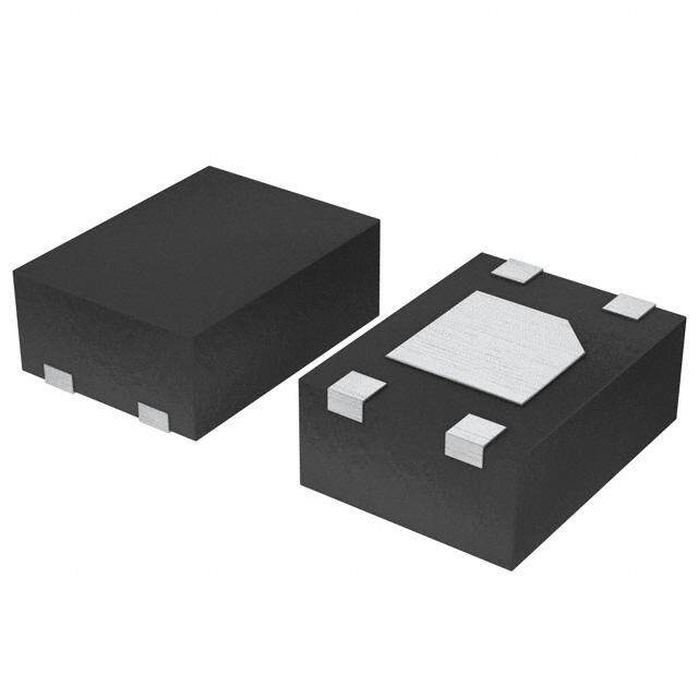
PACKAGE OUTLINE DRB0008B VSON - 1 mm max height SCALE 4.000 PLASTIC SMALL OUTLINE - NO LEAD 3.1 B A 2.9 PIN 1 INDEX AREA 3.1 2.9 C 1 MAX SEATING PLANE 0.05 0.08 C 0.00 EXPOSED 1.65 0.05 (0.2) TYP THERMAL PAD 4 5 2X 1.95 2.4 0.05 8 1 6X 0.65 0.35 8X 0.25 PIN 1 ID 0.5 0.1 C A B (OPTIONAL) 8X 0.3 0.05 C 4218876/A 12/2017 NOTES: 1. All linear dimensions are in millimeters. Any dimensions in parenthesis are for reference only. Dimensioning and tolerancing per ASME Y14.5M. 2. This drawing is subject to change without notice. 3. The package thermal pad must be soldered to the printed circuit board for thermal and mechanical performance. www.ti.com
EXAMPLE BOARD LAYOUT DRB0008B VSON - 1 mm max height PLASTIC SMALL OUTLINE - NO LEAD (1.65) 8X (0.6) SYMM 1 8 8X (0.3) (2.4) (0.95) 6X (0.65) 4 5 (R0.05) TYP (0.575) ( 0.2) VIA (2.8) TYP LAND PATTERN EXAMPLE SCALE:20X 0.07 MAX 0.07 MIN ALL AROUND ALL AROUND SOLDER MASK METAL METAL UNDER SOLDER MASK OPENING SOLDER MASK OPENING NON SOLDER MASK SOLDER MASK DEFINED DEFINED (PREFERRED) SOLDER MASK DETAILS 4218876/A 12/2017 NOTES: (continued) 4. This package is designed to be soldered to a thermal pad on the board. For more information, see Texas Instruments literature number SLUA271 (www.ti.com/lit/slua271). 5. Vias are optional depending on application, refer to device data sheet. If any vias are implemented, refer to their locations shown on this view. It is recommended that vias under paste be filled, plugged or tented. www.ti.com
EXAMPLE STENCIL DESIGN DRB0008B VSON - 1 mm max height PLASTIC SMALL OUTLINE - NO LEAD SYMM 8X (0.6) METAL TYP 1 8X (0.3) 8 (0.63) SYMM 6X (0.65) (1.06) 5 4 (R0.05) TYP (1.47) (2.8) SOLDER PASTE EXAMPLE BASED ON 0.125 mm THICK STENCIL EXPOSED PAD 81% PRINTED SOLDER COVERAGE BY AREA SCALE:25X 4218876/A 12/2017 NOTES: (continued) 6. Laser cutting apertures with trapezoidal walls and rounded corners may offer better paste release. IPC-7525 may have alternate design recommendations. www.ti.com
IMPORTANTNOTICEANDDISCLAIMER TI PROVIDES TECHNICAL AND RELIABILITY DATA (INCLUDING DATASHEETS), DESIGN RESOURCES (INCLUDING REFERENCE DESIGNS), APPLICATION OR OTHER DESIGN ADVICE, WEB TOOLS, SAFETY INFORMATION, AND OTHER RESOURCES “AS IS” AND WITH ALL FAULTS, AND DISCLAIMS ALL WARRANTIES, EXPRESS AND IMPLIED, INCLUDING WITHOUT LIMITATION ANY IMPLIED WARRANTIES OF MERCHANTABILITY, FITNESS FOR A PARTICULAR PURPOSE OR NON-INFRINGEMENT OF THIRD PARTY INTELLECTUAL PROPERTY RIGHTS. These resources are intended for skilled developers designing with TI products. You are solely responsible for (1) selecting the appropriate TI products for your application, (2) designing, validating and testing your application, and (3) ensuring your application meets applicable standards, and any other safety, security, or other requirements. These resources are subject to change without notice. TI grants you permission to use these resources only for development of an application that uses the TI products described in the resource. Other reproduction and display of these resources is prohibited. No license is granted to any other TI intellectual property right or to any third party intellectual property right. TI disclaims responsibility for, and you will fully indemnify TI and its representatives against, any claims, damages, costs, losses, and liabilities arising out of your use of these resources. TI’s products are provided subject to TI’s Terms of Sale (www.ti.com/legal/termsofsale.html) or other applicable terms available either on ti.com or provided in conjunction with such TI products. TI’s provision of these resources does not expand or otherwise alter TI’s applicable warranties or warranty disclaimers for TI products. Mailing Address: Texas Instruments, Post Office Box 655303, Dallas, Texas 75265 Copyright © 2020, Texas Instruments Incorporated