ICGOO在线商城 > 集成电路(IC) > PMIC - 稳压器 - 线性 > TPS79318DBVR
 Datasheet下载
- 型号: TPS79318DBVR
- 制造商: Texas Instruments
- 库位|库存: xxxx|xxxx
- 要求:
| 数量阶梯 | 香港交货 | 国内含税 |
| +xxxx | $xxxx | ¥xxxx |
查看当月历史价格
查看今年历史价格
TPS79318DBVR产品简介:
ICGOO电子元器件商城为您提供TPS79318DBVR由Texas Instruments设计生产,在icgoo商城现货销售,并且可以通过原厂、代理商等渠道进行代购。 TPS79318DBVR价格参考¥2.69-¥4.30。Texas InstrumentsTPS79318DBVR封装/规格:PMIC - 稳压器 - 线性, Linear Voltage Regulator IC Positive Fixed 1 Output 1.8V 200mA SOT-23-5。您可以下载TPS79318DBVR参考资料、Datasheet数据手册功能说明书,资料中有TPS79318DBVR 详细功能的应用电路图电压和使用方法及教程。
TPS79318DBVR是德州仪器(Texas Instruments)生产的一款线性稳压器,属于PMIC(电源管理集成电路)类别。该器件的主要应用场景包括便携式电子设备、工业控制、通信系统等。

 主要应用场景:

1. 便携式电子设备:
   TPS79318DBVR因其低功耗和小封装尺寸,特别适用于对体积和功耗要求严格的便携式设备。例如,智能手机、平板电脑、可穿戴设备(如智能手表、健康监测器)等。这些设备通常需要稳定的电压供应以确保其内部处理器、传感器和其他组件的正常工作,而TPS79318DBVR能够提供高效且稳定的低压输出。

2. 工业控制系统:
   在工业自动化和控制系统中,TPS79318DBVR可以用于为微控制器、传感器、通信模块等提供稳定的电源。其宽输入电压范围(1.6V至5.5V)使其能够在各种复杂的工业环境中稳定工作,同时其低噪声特性有助于提高系统的可靠性和精度。

3. 通信系统:
   通信设备如路由器、交换机、基站等需要多个不同电压等级的电源来支持其内部的各种芯片和模块。TPS79318DBVR可以作为其中的一部分,提供所需的低噪声、高精度的电源,确保通信链路的稳定性和数据传输的准确性。

4. 消费电子产品:
   在消费类电子产品中,如数码相机、MP3播放器、便携式游戏机等,TPS79318DBVR同样有着广泛的应用。它不仅能够提供稳定的电源,还能通过其内置的过热保护和短路保护功能,增强产品的安全性和耐用性。

 特点与优势:

- 低静态电流:典型值仅为20μA,有助于延长电池寿命。
- 低噪声:具有极低的输出噪声,适合对电源质量要求较高的应用。
- 快速瞬态响应:能够迅速响应负载变化,保持输出电压的稳定性。
- 小型封装:采用SOT-23-5封装,节省PCB空间,适合紧凑型设计。
- 内置保护功能:包括过温保护、短路保护等,提高了系统的可靠性。

综上所述,TPS79318DBVR凭借其优异的性能和广泛的适用性,成为众多应用领域的理想选择。
| 参数 | 数值 |
| 产品目录 | 集成电路 (IC)半导体 |
| 描述 | IC REG LDO 1.8V 0.2A SOT23-5低压差稳压器 200mA 1.8V Hi PSRR |
| DevelopmentKit | TPS79318YEQEVM |
| 产品分类 | |
| 品牌 | Texas Instruments |
| 产品手册 | |
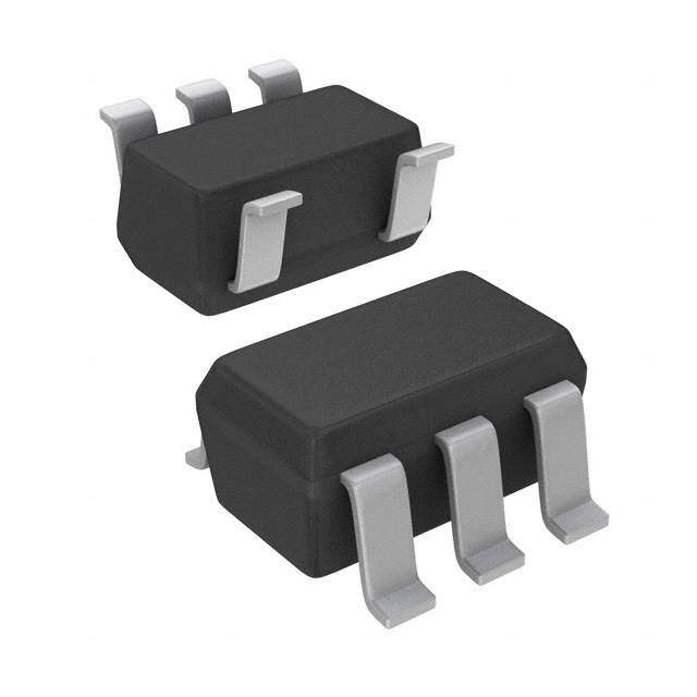
| 产品图片 |
|
| rohs | 符合RoHS无铅 / 符合限制有害物质指令(RoHS)规范要求 |
| 产品系列 | 电源管理 IC,低压差稳压器,Texas Instruments TPS79318DBVR- |
| 数据手册 | |
| 产品型号 | TPS79318DBVR |
| PCN设计/规格 | |
| 产品目录页面 | |
| 产品种类 | 低压差稳压器 |
| 供应商器件封装 | SOT-23-5 |
| 其它名称 | 296-12155-1 |
| 包装 | 剪切带 (CT) |
| 商标 | Texas Instruments |
| 回动电压—最大值 | 55 mV |
| 安装类型 | 表面贴装 |
| 安装风格 | SMD/SMT |
| 封装 | Reel |
| 封装/外壳 | SC-74A,SOT-753 |
| 封装/箱体 | SOT-23-5 |
| 工作温度 | -40°C ~ 150°C |
| 工厂包装数量 | 3000 |
| 最大功率耗散 | 0.56 W |
| 最大工作温度 | + 150 C |
| 最大输入电压 | 5.5 V |
| 最小工作温度 | - 40 C |
| 最小输入电压 | + 2.7 V |
| 标准包装 | 1 |
| 电压-跌落(典型值) | - |
| 电压-输入 | 2.7 V ~ 5.5 V |
| 电压-输出 | 1.8V |
| 电压调节准确度 | 2 % |
| 电流-输出 | 200mA |
| 电流-限制(最小值) | 285mA |
| 稳压器拓扑 | 正,固定式 |
| 稳压器数 | 1 |
| 系列 | TPS79318 |
| 线路调整率 | 0.05 % / V |
| 负载调节 | 5 mV |
| 输入偏压电流—最大 | 0.17 mA |
| 输出电压 | 1.8 V |
| 输出电流 | 200 mA |
| 输出端数量 | 1 Output |
| 输出类型 | Fixed |
| 配用 | /product-detail/zh/TPS79301EVM/296-13593-ND/486551/product-detail/zh/TPS79328EVM/296-13594-ND/486552/product-detail/zh/TPS79318YEQEVM/296-19005-ND/863827/product-detail/zh/TPS79325YEQEVM/296-19006-ND/863828/product-detail/zh/TPS793285YEQEVM/296-19007-ND/863829/product-detail/zh/TPS79328YEQEVM/296-19008-ND/863830/product-detail/zh/TPS79330YEQEVM/296-19010-ND/863832/product-detail/zh/DEM-SOT23LDO/296-20843-ND/1216448 |


- 商务部:美国ITC正式对集成电路等产品启动337调查
- 曝三星4nm工艺存在良率问题 高通将骁龙8 Gen1或转产台积电
- 太阳诱电将投资9.5亿元在常州建新厂生产MLCC 预计2023年完工
- 英特尔发布欧洲新工厂建设计划 深化IDM 2.0 战略
- 台积电先进制程称霸业界 有大客户加持明年业绩稳了
- 达到5530亿美元!SIA预计今年全球半导体销售额将创下新高
- 英特尔拟将自动驾驶子公司Mobileye上市 估值或超500亿美元
- 三星加码芯片和SET,合并消费电子和移动部门,撤换高东真等 CEO
- 三星电子宣布重大人事变动 还合并消费电子和移动部门
- 海关总署:前11个月进口集成电路产品价值2.52万亿元 增长14.8%


PDF Datasheet 数据手册内容提取
Product Sample & Technical Tools & Support & Folder Buy Documents Software Community TPS793 SLVS348L–JULY2001–REVISEDMAY2015 TPS793 Low-Noise, High PSRR, RF, 200-mA Low-Dropout Linear Regulators in NanoStar™ Wafer Chip Scale and SOT-23 1 Features 3 Description • 200-mARFLow-DropoutRegulator The TPS793 family of low-dropout (LDO) low-power 1 linear voltage regulators features high power-supply WithEnable rejection ratio (PSRR), ultralow-noise, fast start-up, • AvailableinFixed-VoltageVersionsfrom1.8Vto and excellent line and load transient responses in 4.75VandAdjustable(1.22Vto5.5V) NanoStar™ wafer chip scale and SOT23 packages. • HighPSRR(70dBat10kHz) NanoStar packaging gives an ultrasmall footprint as well as an ultralow profile and package weight, • LowNoise(32μV ,TPS79328) RMS making these devices ideal for portable applications • FastStart-UpTime(50 μs) such as handsets and PDAs. Each device in the • StableWitha2.2-μFCeramicCapacitor family is stable, with a small, 2.2-μF ceramic • ExcellentLoadandLineTransientResponse capacitor on the output. The TPS793 family uses an advanced, proprietary BiCMOS fabrication process to • VeryLowDropoutVoltage(112mVat200mA, yield extremely low dropout voltages (for example, TPS79330) 112 mV at 200 mA, TPS79330). Each device • 5-and6-PinSOT23(DBV)andNanoStarWafer achieves fast start-up times (approximately 50 μs with ChipScale(YZQ)Packages a 0.001-μF bypass capacitor) while consuming very low quiescent current (170 μA typical). Moreover, 2 Applications when the device is placed in standby mode, the supply current is reduced to less than 1 μA. The • RF:VCOs,Receivers,ADCs TPS79328 exhibits approximately 32 μV of output RMS • Audio voltage noise at 2.8-V output with a 0.1-μF bypass • CellularandCordlessTelephones capacitor. Applications with analog components that are noise-sensitive, such as portable RF electronics, • Bluetooth®,WirelessLAN benefit from the high PSRR and low-noise features • HandheldOrganizers,PDAs aswellasthefastresponsetime. DeviceInformation(1) PARTNUMBER PACKAGE BODYSIZE(NOM) SOT-23(6) 2.90mm×1.60mm TPS793 SOT-23(5) 2.90mm×1.60mm DSBGA(5) 1.35mm×1.00mm (1) For all available packages, see the orderable addendum at theendofthedatasheet. TypicalApplicationCircuit RippleRejectionvsFrequency V V 100 VIN IN IN TPS79328OUT OUT VOUT 90 VCIONU=T3=.82.V2mF 80 CNR=0.1mF 0.1mF EN GND NR 10mF B) IOUT=200mA 0.01mF n (d 70 ctio 60 e Rej 50 IOUT=10mA ple 40 p Ri 30 20 10 0 10 100 1k 10k 100k 1M 10M Frequency (Hz) 1 An IMPORTANT NOTICE at the end of this data sheet addresses availability, warranty, changes, use in safety-critical applications, intellectualpropertymattersandotherimportantdisclaimers.PRODUCTIONDATA.
TPS793 SLVS348L–JULY2001–REVISEDMAY2015 www.ti.com Table of Contents 1 Features.................................................................. 1 8 ApplicationandImplementation........................ 14 2 Applications........................................................... 1 8.1 ApplicationInformation............................................14 3 Description............................................................. 1 8.2 TypicalApplication..................................................15 4 RevisionHistory..................................................... 2 8.3 Do'sandDon'ts.......................................................17 5 PinConfigurationandFunctions......................... 3 9 PowerSupplyRecommendations...................... 17 6 Specifications......................................................... 4 10 Layout................................................................... 18 6.1 AbsoluteMaximumRatings......................................4 10.1 LayoutGuidelines.................................................18 6.2 ESDRatings ............................................................4 10.2 LayoutExample....................................................18 6.3 RecommendedOperatingConditions.......................4 10.3 PowerDissipation.................................................18 6.4 ThermalInformation..................................................5 11 DeviceandDocumentationSupport................. 20 6.5 ElectricalCharacteristics..........................................6 11.1 DeviceSupport......................................................20 6.6 TypicalCharacteristics..............................................7 11.2 DocumentationSupport........................................20 7 DetailedDescription............................................ 11 11.3 CommunityResource............................................20 7.1 Overview.................................................................11 11.4 Trademarks...........................................................21 7.2 FunctionalBlockDiagrams.....................................11 11.5 ElectrostaticDischargeCaution............................21 7.3 FeatureDescription.................................................12 11.6 Glossary................................................................21 7.4 DeviceFunctionalModes........................................13 12 Mechanical,Packaging,andOrderable Information........................................................... 21 4 Revision History ChangesfromRevisionK(October2007)toRevisionL Page • Changedtitleofdatasheet ................................................................................................................................................... 1 • DeletedreferencestoYEQpackagethroughoutdocument(packageisobsolete) .............................................................. 1 • ChangedfourthbulletofFeatureslisttolownoise................................................................................................................ 1 • Changedfront-pagefigure..................................................................................................................................................... 1 • ChangedAbsoluteMaximumRatingsconditionstatement ................................................................................................... 4 • AddedPinConfigurationsandFunctionssection,ESDRatingstable,FeatureDescriptionsection,DeviceFunctional Modes,ApplicationandImplementationsection,PowerSupplyRecommendationssection,Layoutsection,Device andDocumentationSupportsection,andMechanical,Packaging,andOrderableInformationsection .............................. 4 • DeletedDissipationRatingstable;addedThermalInformationtable ................................................................................... 5 • DeletedT =25°CtestconditionfromPSRRspecificationmeasurementsbecauseofredundancy.................................... 6 J • AddedconditionstatementtoTypicalCharacteristics........................................................................................................... 7 • ChangedFigure23;changedcapacitornotationtoC infigureandrelatedtable ............................................................ 14 FF • ChangedFigure24;changedcapacitornotationtoC infigure,changed2.2µFcapacitorvalueto10µF,and FF changeddevicename.......................................................................................................................................................... 15 2 SubmitDocumentationFeedback Copyright©2001–2015,TexasInstrumentsIncorporated ProductFolderLinks:TPS793
TPS793 www.ti.com SLVS348L–JULY2001–REVISEDMAY2015 5 Pin Configuration and Functions DBVPackage 5-PinSOT-23FixedVoltageVersion DBVPackage TopView 6-PinSOT-23AdjustableVoltageVersion TopView IN 1 5 OUT IN 1 6 OUT GND 2 GND 2 5 FB EN 3 4 NR EN 3 4 NR YZQPackage 5-PinDSBGA TopView IN OUT C3 C1 B2 NR A3 A1 EN GND PinFunctions PIN I/O DESCRIPTION NAME DBV YZQ Enablepin.Drivingtheenablepin(EN)highturnsontheregulator.Drivingthispinlowputs EN 3 A3 I theregulatorintoshutdownmode.ENcanbeconnectedtoINifnotused. Feedbackpin.Thisterminalisthefeedbackinputpinfortheadjustabledevice.Fixedvoltage FB 5 — I versionsintheDBVpackagedonothavethispin. GND 2 A1 — Regulatorground. IN 1 C3 I Inputtothedevice. NoiseReductionpin.Connectinganexternalcapacitortothispinfiltersnoisegeneratedby NR 4 B2 — theinternalbandgap.Thisconfigurationimprovespower-supplyrejectionandreducesoutput noise. OUT 6 C1 O Outputoftheregulator. Copyright©2001–2015,TexasInstrumentsIncorporated SubmitDocumentationFeedback 3 ProductFolderLinks:TPS793
TPS793 SLVS348L–JULY2001–REVISEDMAY2015 www.ti.com 6 Specifications 6.1 Absolute Maximum Ratings overoperatingjunctiontemperaturerange(unlessotherwisenoted).AllvoltagesarewithrespecttoGND.(1) MIN MAX UNIT Input,V –0.3 6 V IN Voltage Enable,V –0.3 6 V EN Output,V –0.3 6 V OUT Current Peakoutput,I Internallylimited A OUT(max) Outputshort-circuitduration Indefinite Totalpowerdissipation Continuous,P SeeThermalInformation D(tot) DBVpackage –40 150 °C Junction,T J Temperature YZQpackage –40 125 °C Storage,T –65 150 °C stg (1) StressesbeyondthoselistedunderAbsoluteMaximumRatingsmaycausepermanentdamagetothedevice.Thesearestressratings only,whichdonotimplyfunctionaloperationofthedeviceattheseoranyotherconditionsbeyondthoseindicatedunderRecommended OperatingConditions.Exposuretoabsolute-maximum-ratedconditionsforextendedperiodsmayaffectdevicereliability. 6.2 ESD Ratings VALUE UNIT Humanbodymodel(HBM),perANSI/ESDA/JEDECJS-001,allpins(1) ±2000 V(ESD) Electrostaticdischarge Chargeddevicemodel(CDM),perJEDECspecificationJESD22-C101, V allpins(2) ±500 (1) JEDECdocumentJEP155statesthat500-VHBMallowssafemanufacturingwithastandardESDcontrolprocess. (2) JEDECdocumentJEP157statesthat250-VCDMallowssafemanufacturingwithastandardESDcontrolprocess. 6.3 Recommended Operating Conditions overoperatingjunctiontemperaturerange(unlessotherwisenoted). MIN NOM MAX UNIT V Inputsupplyvoltagerange 2.7 5.5 V IN V Enablesupplyvoltagerange 0 V V EN IN V Outputvoltagerange V 5 V OUT FB I Outputcurrent 0 200 mA OUT T Operatingjunctiontemperature –40 125 °C J C Inputcapacitor 0.1 1 µF IN C Outputcapacitor 2.2(1) 10 µF OUT C Noisereductioncapacitor 0 10 nF NR C Feed-forwardcapacitor 15 pF FF R Lowerfeedbackresistor 30.1 kΩ 2 (1) IfC isnotusedorV <1.8V,theminimumrecommendedC =4.7µF. FF OUT(nom) OUT 4 SubmitDocumentationFeedback Copyright©2001–2015,TexasInstrumentsIncorporated ProductFolderLinks:TPS793
TPS793 www.ti.com SLVS348L–JULY2001–REVISEDMAY2015 6.4 Thermal Information TPS79301 THERMALMETRIC(1) DBV(SOT-23) YZQ(DSBGA) UNIT 6PINS 5PINS R Junction-to-ambientthermalresistance 225.1 178.5 °C/W θJA R Junction-to-case(top)thermalresistance 78.4 1.4 °C/W θJC(top) R Junction-to-boardthermalresistance 54.7 62.1 °C/W θJB ψ Junction-to-topcharacterizationparameter 3.3 0.9 °C/W JT ψ Junction-to-boardcharacterizationparameter 53.8 62.1 °C/W JB (1) Formoreinformationabouttraditionalandnewthermalmetrics,seetheSemiconductorandICPackageThermalMetricsapplication report,SPRA953. Copyright©2001–2015,TexasInstrumentsIncorporated SubmitDocumentationFeedback 5 ProductFolderLinks:TPS793
TPS793 SLVS348L–JULY2001–REVISEDMAY2015 www.ti.com 6.5 Electrical Characteristics OverrecommendedoperatingtemperaturerangeT =–40°Cto125°C,V =V ,V =V +1V(1),I =1mA,C = J EN IN IN OUT(nom) OUT OUT 10μF,C =0.01μF(unlessotherwisenoted).TypicalvaluesareatT =25°C. NR J PARAMETER TESTCONDITIONS MIN TYP MAX UNIT V Inputvoltagerange(1) 2.7 5.5 V IN I Continuousoutputcurrent 0 200 mA OUT V Internalreference(TPS79301) 1.201 1.225 1.250 V FB TPS79301 V 5.5–V FB DO TPS79318 0µA<I <200mA,2.8V<V <5.5V 1.764 1.8 1.836 OUT IN TPS79325 0µA<I <200mA,3.5V<V <5.5V 2.45 2.5 2.55 OUT IN Outputvoltage TPS79328 0µA<IOUT<200mA,3.8V<VIN<5.5V 2.744 2.8 2.856 V V OUT range TPS793285 0µA<I <200mA,3.85V<V <5.5V 2.793 2.85 2.907 OUT IN TPS79330 0µA<I <200mA,4V<V <5.5V 2.94 3 3.06 OUT IN TPS79333 0µA<I <200mA,4.3V<V <5.5V 3.234 3.3 3.366 OUT IN TPS793475 0µA<I <200mA,5.25V<V <5.5V 4.655 4.75 4.845 OUT IN ΔV Lineregulation V +1V<V ≤5.5V 0.05 0.12 %/V OUT(ΔVIN) OUT IN ΔV Loadregulation 0µA<I <200mA,T =25°C 5 mV OUT(ΔIOUT) OUT J TPS79328 I =200mA 120 200 OUT Dropout TPS793285 I =200mA 120 200 OUT voltage(2) V TPS79330 I =200mA 112 200 mV DO (V =V – OUT IN OUT(nom) 0.1V) TPS79333 IOUT=200mA 12 180 TPS793475 I =200mA 77 125 OUT I Outputcurrentlimit V =0V 285 600 mA CL OUT I Groundpincurrent 0µA<I <200mA 170 220 µA GND OUT I Shutdowncurrent(3) V =0V,2.7V<V <5.5V 0.07 1 µA SHUTDOWN EN IN I FBpincurrent V =1.8V 1 µA FB FB f=100Hz,I =10mA 70 OUT Power-supply f=100Hz,IOUT=200mA 68 PSRR TPS79328 dB rejectionratio f=10kHz,I =200mA 70 OUT f=100kHz,I =200mA 43 OUT C =0.001μF 55 NR Outputnoise BW=200Hzto CNR=0.0047μF 36 V TPS79328 100kHz, µV n voltage IOUT=200mA CNR=0.01μF 33 RMS C =0.1μF 32 NR C =0.001μF 50 NR R =14Ω, t Startuptime TPS79328 L C =0.0047μF 70 µs STR C =1µF NR OUT C =0.01μF 100 NR V High-levelenableinputvoltage 2.7V<V <5.5V 1.7 V V EN(high) IN IN V Low-levelenableinputvoltage 2.7V<V <5.5V 0 0.7 V EN(low) IN I ENpincurrent V =0V –1 1 µA EN EN Threshold,V rising 2.25 2.65 V CC UVLO Hysteresis 100 mV (1) MinimumV is2.7VorV +V ,whicheverisgreater. IN OUT DO (2) DropoutisnotmeasuredfortheTPS79318andTPS79325becauseminimumV =2.7V. IN (3) Foradjustableversions,thisparameterappliesonlyafterV isapplied;thenV transitionshightolow. IN EN 6 SubmitDocumentationFeedback Copyright©2001–2015,TexasInstrumentsIncorporated ProductFolderLinks:TPS793
TPS793 www.ti.com SLVS348L–JULY2001–REVISEDMAY2015 6.6 Typical Characteristics OverrecommendedoperatingtemperaturerangeT =–40°Cto125°C,V =V ,V =V +1V,I =1mA,C = J EN IN IN OUT(nom) OUT OUT 10μF,C =0.01μF,V =2.8V(unlessotherwisenoted).TypicalvaluesareatT =25°C. NR OUT(nom) J 2.805 2.805 2.804 VIN=3.8V COUT=10mF 2.800 2.803 TJ=25°C IOUT=1mA 2.802 2.795 2.801 V) V) (OUT 2.800 (OUT2.790 V 2.799 V IOUT=200mA 2.785 2.798 2.797 2.780 2.796 VIN=3.8V COUT=10mF 2.795 2.775 0 50 100 150 200 −40−25−105 20 35 50 65 80 95 110125 IOUT(mA) TJ(°C) Figure1.TPS79328OutputVoltagevsOutputCurrent Figure2.TPS79328OutputVoltagevsJunction Temperature 250 0.30 VCIONU=T3=.810VmF IOUT=1mA √H)z 0.25 VCIONU=T3=.82.V2mF 200 V/m CNR=0.1mF y ( A) 150 IOUT=200mA Densit 0.20 I(mGND 100 al Noise 0.15 IOUT=1mA ctr 0.10 50 ut Spe 0.05 IOUT=200mA p ut O 0 0 −40−25−105 20 35 50 65 80 95110125 100 1k 10k 100k TJ(°C) Frequency (Hz) Figure3.TPS79328GroundCurrentvsJunction Figure4.TPS79328OutputSpectralNoiseDensityvs Temperature Frequency 0.30 1.6 √V/)HzNoise Density (m 000...122505 IOUT=1VCCIONmNRUA=T=3=0.8.110VmmFF √V)/HzNoise Density (m 0111....8024 CNCRN=RC0N=.0R00=.10VICO00mIO.4NUF0U7T1=Tm=m3=FF2.81000VmmFA Spectral 0.10 IOUT=200mA Spectral 00..46 CNR=0.1mF Output 0.05 Output 0.2 0 0 100 1k 10k 100k 100 1k 10k 100k Frequency (Hz) Frequency (Hz) Figure5.TPS79328OutputSpectralNoiseDensityvs Figure6.TPS79328OutputSpectralNoiseDensityvs Frequency Frequency Copyright©2001–2015,TexasInstrumentsIncorporated SubmitDocumentationFeedback 7 ProductFolderLinks:TPS793
TPS793 SLVS348L–JULY2001–REVISEDMAY2015 www.ti.com Typical Characteristics (continued) OverrecommendedoperatingtemperaturerangeT =–40°Cto125°C,V =V ,V =V +1V,I =1mA,C = J EN IN IN OUT(nom) OUT OUT 10μF,C =0.01μF,V =2.8V(unlessotherwisenoted).TypicalvaluesareatT =25°C. NR OUT(nom) J 60 2.5 )S 50 IOCVUOOTUU=TT2==01020.8mmVAF 2.0 VCTJION=U=T235=.°81(cid:3)C0VmF M R V 40 e ( 1.5 s Output Noi 2300 ZO ()W 1.0 IOUITOU=T1=001mmAA S, RM 10 0.5 BW=100Hzto100kHz 0 00 0.001 0.01 0.1 10 100 1k 10k 100k 1M 10M CNR(mF) Frequency (Hz) Figure7.RootMeanSquareOutputNoisevsC Figure8.OutputImpedancevsFrequency NR 180 100 VIN=2.7V 160 COUT=10mF 90 IOUT=200mA 140 80 B) 70 mV) 110200 IOUT=200mA ction (d 60 (DO 80 Reje 50 V 60 Ripple 4300 IOUT=10mA 2400 IOUT=10mA 1200 VCIONU=T3=.810VmF 0 0 CNR=0.01mF −40−25−10 5 20 35 50 65 80 95110125 10 100 1k 10k 100k 1M 10M TJ(°C) Frequency (Hz) Figure9.TPS79328DropoutVoltagevsJunction Figure10.TPS79328RippleRejectionvsFrequency Temperature 100 100 90 VCIONU=T3=.82.V2mF 90 VCIONU=T3=.82.V2mF 80 CNR=0.01mF 80 CNR=0.1mF B) IOUT=200mA B) IOUT=200mA n (d 70 n (d 70 ctio 60 ctio 60 ple Reje 4500 IOUT=10mA ple Reje 4500 IOUT=10mA p p Ri 30 Ri 30 20 20 10 10 0 0 10 100 1k 10k 100k 1M 10M 10 100 1k 10k 100k 1M 10M Frequency (Hz) Frequency (Hz) Figure11.TPS79328RippleRejectionvsFrequency Figure12.TPS79328RippleRejectionvsFrequency 8 SubmitDocumentationFeedback Copyright©2001–2015,TexasInstrumentsIncorporated ProductFolderLinks:TPS793
TPS793 www.ti.com SLVS348L–JULY2001–REVISEDMAY2015 Typical Characteristics (continued) OverrecommendedoperatingtemperaturerangeT =–40°Cto125°C,V =V ,V =V +1V,I =1mA,C = J EN IN IN OUT(nom) OUT OUT 10μF,C =0.01μF,V =2.8V(unlessotherwisenoted).TypicalvaluesareatT =25°C. NR OUT(nom) J 4 4.8 V) V) m (N 2 VIN=3.8V (T VE VOUT=2.8V OU 0 IOUT=200mA V 3.8 COUT=2.2mF IOUT=200mA 3 CNR=0.001mF TJ=25°C 20 CCONRUT==0.20.12mmFF ddvt =0m.4sV V) (V)OUT 12 CNR=0.0047mF V(mIN -200 V CNR=0.01mF 0 0 20 40 60 80 100120140160180200 0 10 20 30 40 50 60 70 80 90 100 Time (ms) Time (ms) Figure13.TPS79328OutputVoltage,EnableVoltagevs Figure14.TPS79328LineTransientResponse Time(Start-Up) V) 20 VCIONU=T3=.810VmF VROLU=T1=53WV (m 0 UT VO −20 v D di −40 mV/ 0 A) 230000 ddti =0.m02sA 50 VIN VOUT m (UT 100 1mA O I 0 0 50100 150200 250300 350400450500 1s/div Time (ms) Figure15.TPS79328LoadTransientResponse Figure16.Power-UpandPower-Down 250 200 200 TJ=125°C 150 TJ=125°C V(mV)DO 110500 TJ=25°C V(mV)DO 100 TJ=25°C 50 TJ=−55°C 50 TJ=−40°C IOUT=200mA 0 0 0 20 40 60 80 100120140160180 200 2.5 3.0 3.5 4.0 4.5 5.0 IOUT(mA) VIN(V) Figure17.DropoutVoltagevsOutputCurrent Figure18.TPS79301DropoutVoltagevsInputVoltage Copyright©2001–2015,TexasInstrumentsIncorporated SubmitDocumentationFeedback 9 ProductFolderLinks:TPS793
TPS793 SLVS348L–JULY2001–REVISEDMAY2015 www.ti.com Typical Characteristics (continued) OverrecommendedoperatingtemperaturerangeT =–40°Cto125°C,V =V ,V =V +1V,I =1mA,C = J EN IN IN OUT(nom) OUT OUT 10μF,C =0.01μF,V =2.8V(unlessotherwisenoted).TypicalvaluesareatT =25°C. NR OUT(nom) J 100 100 nce()W VTCJION=U=T−54=.052°.CV2,tmVoFO1U2T5°≥C1.5V nce()W CVTJION=U=T−54=.051°0CVmtoF125°C Resista 10 RegionofInstability Resista 10 RegionofInstability Series 1 Series 1 nt nt uivale 0.1 uivale 0.1 R,Eq RegionofStability R,Eq RegionofStability S S E E 0.01 0.01 0 0.02 0.04 0.06 0.08 0.20 0 0.02 0.04 0.06 0.08 0.20 IOUT(A) IOUT(A) Figure19.TypicalRegionsofStabilityEquivalentSeries Figure20.TypicalRegionsofStabilityEquivalentSeries Resistance(ESR)vsOutputCurrent Resistance(ESR)vsOutputCurrent 10 SubmitDocumentationFeedback Copyright©2001–2015,TexasInstrumentsIncorporated ProductFolderLinks:TPS793
TPS793 www.ti.com SLVS348L–JULY2001–REVISEDMAY2015 7 Detailed Description 7.1 Overview The TPS793 family of LDO regulators has been optimized for use in noise-sensitive battery-operated equipment. The device features extremely low dropout voltages, high PSRR, ultralow output noise, low quiescent current (170μAtypically),andenable-inputtoreducesupplycurrentstolessthan1 μAwhentheregulatoristurnedoff. 7.2 Functional Block Diagrams IN OUT UVLO Current 59 k 2.45 V Sense ILIM SHUTDOWN R1 GND _ + FB EN R2 UVLO Thermal Shutdown External to QuickStart the Device IN RBeafnedregnacpe 250 kW Vref NR 1.22 V Figure21. TPS79301BlockDiagram(AdjustableVersion) IN OUT UVLO 2.45 V Current Sense GND SHUTDOWN ILIM R1 _ + EN UVLO R2 Thermal Shutdown QuickStart R2 = 40 kW Bandgap 250 kW Vref IN Reference NR 1.22 V Figure22. TPS793BlockDiagram(FixedVersion) Copyright©2001–2015,TexasInstrumentsIncorporated SubmitDocumentationFeedback 11 ProductFolderLinks:TPS793
TPS793 SLVS348L–JULY2001–REVISEDMAY2015 www.ti.com 7.3 Feature Description 7.3.1 UndervoltageLockout(UVLO) The TPS793 uses an undervoltage lockout (UVLO) circuit that disables the output until the input voltage is greater than the rising UVLO voltage. This circuit ensures that the device does not exhibit any unpredictable behaviorwhenthesupplyvoltageislowerthantheoperationalrangeoftheinternalcircuitry,V . IN(min) 7.3.2 Shutdown The enable pin (EN) is active high. Enable the device by forcing the EN pin to exceed V (1.7 V, minimum). EN(high) Turn off the device by forcing the EN pin to drop below 0.7 V. If shutdown capability is not required, connect EN toIN. 7.3.3 FoldbackCurrentLimit The TPS793 features internal current limiting and thermal protection. During normal operation, the TPS793 limits output current to approximately 400 mA. When current limiting engages, the output voltage scales back linearly until the overcurrent condition ends. While current limiting is designed to prevent gross device failure, care should be taken not to exceed the power dissipation ratings of the package or the absolute maximum voltage ratingsofthedevice. 7.3.4 ThermalProtection Thermal protection disables the output when the junction temperature rises to approximately 165°C, allowing the device to cool. When the junction temperature cools to approximately 140°C, the output circuitry is again enabled. Depending on power dissipation, thermal resistance, and ambient temperature, the thermal protection circuit may cycle on and off. This cycling limits regulator dissipation, protecting the device from damage as a resultofoverheating. Any tendency to activate the thermal protection circuit indicates excessive power dissipation or an inadequate heatsink.Forreliableoperation,junctiontemperaturemustbelimitedto125°Cmaximum.Toestimatethemargin of safety in a complete design (including heatsink), increase the ambient temperature until the thermal protection istriggered;useworst-caseloadsandsignalconditions. The TPS793 internal protection circuitry is designed to protect against overload conditions. This circuitry is not intended to replace proper heatsinking. Continuously running the TPS793 into thermal shutdown degrades devicereliability. 7.3.5 ReverseCurrentOperation The TPS793 PMOS-pass transistor has a built-in back diode that conducts reverse current when the input voltage drops below the output voltage (for example, during power down). Current is conducted from the output to the input and is not internally limited. If extended reverse voltage operation is anticipated, external limiting to 5%oftheratedoutputcurrentisrecommended. 12 SubmitDocumentationFeedback Copyright©2001–2015,TexasInstrumentsIncorporated ProductFolderLinks:TPS793
TPS793 www.ti.com SLVS348L–JULY2001–REVISEDMAY2015 7.4 Device Functional Modes 7.4.1 NormalOperation Thedeviceregulatestothenominaloutputvoltageunderthefollowingconditions: • TheinputvoltageisatleastashighasV . IN(min) • Theinputvoltageisgreaterthanthenominaloutputvoltageaddedtothedropoutvoltage. • TheenablevoltageisgreaterthanV . EN(min) • Theoutputcurrentislessthanthecurrentlimit. • Thedevicejunctiontemperatureislessthanthemaximumspecifiedjunctiontemperature. 7.4.2 DropoutOperation If the input voltage is lower than the nominal output voltage plus the specified dropout voltage, but all other conditions are met for normal operation, the device operates in dropout mode. In this mode of operation, the output voltage is the same as the input voltage minus the dropout voltage. The transient performance of the deviceissignificantlydegradedbecausethepassdeviceisinthelinearregionandnolongercontrolsthecurrent throughtheLDO.Lineorloadtransientsindropoutcanresultinlargeoutputvoltagedeviations. 7.4.3 Disabled Thedeviceisdisabledunderthefollowingconditions: • The enable voltage is less than the enable falling threshold voltage or has not yet exceeded the enable rising threshold. • Thedevicejunctiontemperatureisgreaterthanthethermalshutdowntemperature. • TheinputvoltageislessthanUVLO . falling Table1showstheconditionsthatleadtothedifferentmodesofoperation. Table1.DeviceFunctionalModeComparison PARAMETER OPERATINGMODE V V I T IN EN OUT J V >V +V and Normalmode IN OUT(nom) DO V >V I <I T <125°C V >V EN EN(high) OUT LIM J IN IN(min) Dropoutmode V <V <V +V V >V — T <125°C IN(min) IN OUT(nom) DO EN EN(high) J Disabledmode (anytrueconditiondisablesthe V <UVLO V <V — T >165°C(1) IN falling EN EN(low) J device) (1) Approximatevalueforthermalshutdown. Copyright©2001–2015,TexasInstrumentsIncorporated SubmitDocumentationFeedback 13 ProductFolderLinks:TPS793
TPS793 SLVS348L–JULY2001–REVISEDMAY2015 www.ti.com 8 Application and Implementation NOTE Information in the following applications sections is not part of the TI component specification, and TI does not warrant its accuracy or completeness. TI’s customers are responsible for determining suitability of components for their purposes. Customers should validateandtesttheirdesignimplementationtoconfirmsystemfunctionality. 8.1 Application Information The TPS793 family of LDO regulators has been optimized for use in noise-sensitive battery-operated equipment. The device features extremely low dropout voltages, high PSRR, ultralow output noise, low quiescent current (170μAtypically),andenable-inputtoreducesupplycurrentstolessthan1 μAwhentheregulatoristurnedoff. 8.1.1 AdjustableOperation The output voltage of the TPS79301 adjustable regulator is programmed using an external resistor divider as showninFigure23.TheoutputvoltageiscalculatedusingEquation1: æ R ö VOUT = VREF´ç1+R1÷ è 2ø where: • V =1.2246Vtyp(theinternalreferencevoltage) (1) REF Resistors R and R should be chosen for approximately 50-μA divider current. Lower value resistors can be 1 2 used for improved noise performance, but the solution consumes more power. Higher resistors values can cause accuracy issues and other problems. The recommended design procedure is to choose R = 30.1 kΩ to set the 2 dividercurrentat50μA,C =15pFforstability,andthencalculateR usingEquation2: FF 1 æV ö R1 =çVOUT -1÷´R2 è REF ø (2) To improve the stability of the adjustable version, it is suggested that a small compensation capacitor be placed between OUT and FB. For output voltages less than 1.8 V, the value of this capacitor should be 100 pF. For output voltages greater than 1.8 V, the approximate value of this capacitor can be calculated as shown in Equation3: (3´10-7)´(R + R ) C = 1 2 FF (R ´R ) 1 2 (3) The suggested value of this capacitor for several resistor ratios is shown in the table in Figure 23. If this capacitorisnotused(suchasinaunity-gainconfiguration)orifanoutputvoltagelessthan1.8Vischosen,then theminimumrecommendedoutputcapacitoris4.7μFinsteadof2.2 μF. OUTPUT VOLTAGE PROGRAMMING GUIDE VIN IN OUT VOUT TPS79301 OUTPUT 1mF EN R1 CFF VOLTAGE R1 R2 CFF 2.2mF NR GND FB 1.22V short open 0pF 0.01mF R2 2.5V 31.6kW 30.1kW 22pF 3.3V 51kW 30.1kW 15pF 3.6V 59kW 30.1kW 15pF Figure23. TPS79301AdjustableLDORegulatorProgramming 14 SubmitDocumentationFeedback Copyright©2001–2015,TexasInstrumentsIncorporated ProductFolderLinks:TPS793
TPS793 www.ti.com SLVS348L–JULY2001–REVISEDMAY2015 8.2 Typical Application AtypicalapplicationcircuitisshowninFigure24. V V V IN IN OUT OUT V IN OUT TPS79328 0.1mF EN GND NR 10mF 0.01mF Figure24. TypicalApplicationCircuit 8.2.1 DesignRequirements Table2liststhedesignrequirements. Table2.DesignParameters PARAMETER DESIGNREQUIREMENT Inputvoltage 4.2Vto3V(LithiumIonbattery) Outputvoltage 1.8V,±1% DCoutputcurrent 10mA Peakoutputcurrent 75mA Maximumambienttemperature 65°C 8.2.2 DetailedDesignProcedure Pick the desired output voltage option. An input capacitor of 0.1 µF is used as the battery is connected to the input through a via and a short 10-mil (0.01-in) trace. An output capacitor of 10 µF is used to provide optimal response time for the load transient. Verify that the maximum junction temperature is not exceed by referring to Figure30. 8.2.2.1 CapacitorRecommendations Low equivalent series resistance (ESR) capacitors should be used for the input, output, noise reduction, and bypass capacitors. Ceramic capacitors with X7R and X5R dielectrics are preferred. These dielectrics offer more stable characteristics. Ceramic X7R capacitors offer improved over-temperature performance, while ceramic X5R capacitorsaremorecost-effectiveandareavailableinhighervalues. 8.2.2.2 InputandOutputCapacitorRequirements A 0.1-μF or larger ceramic input bypass capacitor, connected between IN and GND and located close to the TPS793, is required for stability and improves transient response, noise rejection, and ripple rejection. A higher- value input capacitor may be necessary if large, fast-rise-time load transients are anticipated or the device is locatedseveralinchesfromthepowersource. Like most low-dropout regulators, the TPS793 requires an output capacitor connected between OUT and GND to stabilize the internal control loop. The minimum recommended capacitance is 2.2 μF. Any 2.2-μF or larger ceramic capacitor is suitable, provided the capacitance does not vary significantly over temperature. If load current is not expected to exceed 100 mA, a 1.0-μF ceramic capacitor can be used. If a feed-forward capacitor is not used (such as in a unity-gain configuration) or if an output voltage less than 1.8 V is chosen, then the minimum recommended output capacitor is 4.7 μF instead of 2.2 μF. Table 3 lists the recommended output capacitorsizesforseveralcommonconfigurations. Copyright©2001–2015,TexasInstrumentsIncorporated SubmitDocumentationFeedback 15 ProductFolderLinks:TPS793
TPS793 SLVS348L–JULY2001–REVISEDMAY2015 www.ti.com Table3.OutputCapacitorSizing Condition C (µF) OUT V <1.8VorC =0nF 4.7 OUT FF V >1.8V,I >100mA 2.2 OUT OUT V >1.8V,I <100mA 1 OUT OUT 8.2.2.3 NoiseReductionandFeed-ForwardCapacitorRequirements The internal voltage reference is a key source of noise in an LDO regulator. The TPS793 has an NR pin which is connected to the voltage reference through a 250-kΩ internal resistor. The 250-kΩ internal resistor, in conjunction with an external bypass capacitor connected to the NR pin, creates a low-pass filter to reduce the voltage reference noise and, therefore, the noise at the regulator output. In order for the regulator to operate properly, the current flow out of the NR pin must be at a minimum, because any leakage current creates an IR drop across the internal resistor, thus creating an output error. Therefore, the bypass capacitor must have minimal leakage current. The bypass capacitor should be no more than 0.1 μF to ensure that it is fully charged duringthequickstarttimeprovidedbytheinternalswitchshownintheFunctionalBlockDiagrams. As an example, the TPS79328 exhibits only 32 μV of output voltage noise using a 0.1-μF ceramic bypass RMS capacitor and a 2.2-μF ceramic output capacitor. Note that the output starts up slower as the bypass capacitance increases due to the RC time constant at the NR pin that is created by the internal 250-kΩ resistor and external capacitor. This RC time constant is affected by the quick-start circuit, especially for values near or below 10 nF. SeeFigure13foracomparisonsofC capacitorsandstartuptimes. NR A feed-forward capacitor is recommended to improve the stability of the device. If R = 30.1 kΩ, set C to 15 pF 2 1 for optimal performance. For voltages less than 1.8 V, the value of this capacitor should be 100 pF. For voltages greaterthan1.8V,theapproximatevalueofthiscapacitorcanbecalculatedasshowninEquation3. 8.2.3 ApplicationCurves 4 4.8 V) V) m (N 2 VIN=3.8V (T VE VOUT=2.8V OU 0 IOUT=200mA V 3.8 COUT=2.2mF IOUT=200mA 3 CNR=0.001mF TJ=25°C 20 CCONRUT==0.20.12mmFF ddvt =0m.4sV V) (V)OUT 12 CNR=0.0047mF V(mIN -200 V CNR=0.01mF 0 0 20 40 60 80 100120140160180200 0 10 20 30 40 50 60 70 80 90 100 Time (ms) Time (ms) Figure25.TPS79328OutputVoltage,EnableVoltagevs Figure26.TPS79328LineTransientResponse Time(Start-Up) 16 SubmitDocumentationFeedback Copyright©2001–2015,TexasInstrumentsIncorporated ProductFolderLinks:TPS793
TPS793 www.ti.com SLVS348L–JULY2001–REVISEDMAY2015 100 VIN=3.8V )W COUT=10mF 20 COUT=10mF e( VIN=5.5V V(mV)OUT −200 Resistanc 10 TJ=−40°Cto125R°CegionofInstability D s e −40 eri S 1 300 ddti =0.m02sA alent mA) 200 quiv 0.1 (UT 100 1mA R,E RegionofStability IO ES 0 0.01 0 50100 150200 250300 350400450500 0 0.02 0.04 0.06 0.08 0.20 Time (ms) IOUT(A) Figure27.TPS79328LoadTransientResponse Figure28.TypicalRegionsofStabilityEquivalentSeries Resistance(ESR)vsOutputCurrent 8.3 Do's and Don'ts Do place at least one, low ESR, 2.2-μF capacitor as close as possible between the OUT pin of the regulator and theGNDpin. Do place at least one, low ESR, 0.1-μF capacitor as close as possible between the IN pin of the regulator and theGNDpin. Doprovideadequatethermalpathsawayfromthedevice. Donotplacetheinputoroutputcapacitormorethan10mmawayfromtheregulator. Donotexceedtheabsolutemaximumratings. DonotfloattheEnable(EN)pin. DonotresistivelyorinductivelyloadtheNRpin. Donotlettheoutputvoltagegetmorethan0.3Vabovetheinputvoltage. 9 Power Supply Recommendations These devices are designed to operate from an input voltage supply range from 2.7 V to 5.5 V. The input voltage range must provide adequate headroom in order for the device to have a regulated output. This input supply must be well-regulated and stable. A 0.1-µF input capacitor is required for stability; if the input supply is noisy, additionalinputcapacitorswithlowESRcanhelpimprovetheoutputnoiseperformance. Copyright©2001–2015,TexasInstrumentsIncorporated SubmitDocumentationFeedback 17 ProductFolderLinks:TPS793
TPS793 SLVS348L–JULY2001–REVISEDMAY2015 www.ti.com 10 Layout 10.1 Layout Guidelines Layout is a critical part of good power-supply design. There are several signal paths that conduct fast-changing currents or voltages that can interact with stray inductance or parasitic capacitance to generate noise or degrade the power-supply performance. To help eliminate these problems, the IN pin should be bypassed to ground with alowESRceramicbypasscapacitorwithanX5RorX7Rdielectric. Equivalent series inductance (ESL) and equivalent series resistance (ESR) must be minimized to maximize performanceandensurestability.Everycapacitor(C ,C ,C ,C )mustbeplacedascloseaspossibleto IN OUT NR/SS FF thedeviceandonthesamesideofthePCBastheregulatoritself. DonotplaceanyofthecapacitorsontheoppositesideofthePCBfromwheretheregulatorisinstalled.Theuse of vias and long traces is strongly discouraged because these circuits may impact system performance negatively,andevencauseinstability. 10.1.1 BoardLayoutRecommendationstoImprovePSRRandNoisePerformance ToimproveacmeasurementslikePSRR,outputnoise,andtransientresponse,itisrecommendedthattheboard be designed with separate ground planes for V and V , with each ground plane connected only at the GND IN OUT pin of the device. In addition, the ground connection for the bypass capacitor should connect directly to the GND pinofthedevice. 10.2 Layout Example Output Ground Output Plane Input Plane IN OUT GND FB EN NR Input Ground NR and FB Ground Denotes via Figure29. LayoutExample(DBVPackage) 10.3 Power Dissipation The ability to remove heat from the die is different for each package type, presenting different considerations in the printed circuit board (PCB) layout. The PCB area around the device that is free of other components moves the heat from the device to the ambient air. Performance data for JEDEC low- and high-K boards are given in Thermal Information. Using heavier copper increases the effectiveness in removing heat from the device. The additionofplatedthrough-holestoheat-dissipatinglayersalsoimprovestheheatsinkeffectiveness. Power dissipation depends on input voltage and load conditions. Power dissipation (P ) can be approximated by D the product of the output current times the voltage drop across the output pass element (V to V ), as shown IN OUT inEquation4. 3 (cid:11)9 – 9 (cid:12)u, D IN OUT OUT (4) 18 SubmitDocumentationFeedback Copyright©2001–2015,TexasInstrumentsIncorporated ProductFolderLinks:TPS793
TPS793 www.ti.com SLVS348L–JULY2001–REVISEDMAY2015 Power Dissipation (continued) Power dissipation resulting from quiescent current is negligible. Excessive power dissipation triggers the thermal protectioncircuit. Figure 30 shows the maximum ambient temperature versus the power dissipation of the TPS730. This figure assumes the device is soldered on a JEDEC standard, high-K layout with no airflow over the board. Actual board thermal impedances vary widely. If the application requires high power dissipation, having a thorough understanding of the board temperature and thermal impedances is helpful to ensure the TPS730 does not operateaboveajunctiontemperatureof125°C. 125 DBV Package C) YZQ Package q e ( ur at er 100 p m e T nt e bi m A 75 m u m xi a M 50 0 0.1 0.2 0.3 0.4 0.5 Power Dissapation (W) Figure30. MaximumAmbientTemperaturevsPowerDissipation Estimating the junction temperature can be done by using the thermal metrics Ψ and Ψ , shown in Thermal JT JB Information. These metrics are a more accurate representation of the heat transfer characteristics of the die and thepackagethanR .ThejunctiontemperaturecanbeestimatedwithEquation5. θJA Y : T = T +Y ·P JT J T JT D Y : T = T +Y ·P JB J B JB D where • P isthepowerdissipationshownbyEquation4. D • T isthetemperatureatthecenter-topoftheICpackage. T • T isthePCBtemperaturemeasured1mmawayfromtheICpackageonthePCBsurface. (5) B NOTE Both T and T can be measured on actual application boards using a thermo-gun (an T B infraredthermometer). For more information about measuring T and T , see the application note Using New Thermal Metrics T B (SBVA025),availablefordownloadatwww.ti.com. Copyright©2001–2015,TexasInstrumentsIncorporated SubmitDocumentationFeedback 19 ProductFolderLinks:TPS793
TPS793 SLVS348L–JULY2001–REVISEDMAY2015 www.ti.com 11 Device and Documentation Support 11.1 Device Support 11.1.1 DevelopmentSupport 11.1.1.1 EvaluationModules Seven evaluation modules (EVMs) are available to assist in the initial circuit performance evaluation using the TPS793: • TPS79301EVM • TPS79318YEQEVM • TPS79325YEQEVM • TPS793285YEQEVM • TPS79328EVM • TPS79328YEQEVM • TPS79330YEQEVM These EVMs can be requested at the Texas Instruments website through the device product folders or purchaseddirectlyfromtheTIeStore. 11.1.1.2 SpiceModels Computer simulation of circuit performance using SPICE is often useful when analyzing the performance of analog circuits and systems. A SPICE model for the TPS793 is available through the product folders under Tools &Software. 11.1.2 DeviceNomenclature Table4.OrderingInformation(1)(2) PRODUCT V OUT XX(X)isthenominaloutputvoltage(forexample,28=2.8V;285=2.85V;01=adjustableversion). TPS793xxyyyz YYYisthepackagedesignator. Zisthepackagequantity.Risforreel(3000pieces),Tisfortape(250pieces). (1) ForthemostcurrentpackageandorderinginformationseethePackageOptionAddendumattheendofthisdocument,orvisitthe deviceproductfolderonwww.ti.com. (2) Outputvoltagesfrom1.2Vto4.8Vin50-mVincrementsareavailable.Contactthefactoryfordetailsandavailability. 11.2 Documentation Support 11.2.1 RelatedDocumentation • Applicationnote,UsingNewThermalMetrics,SBVA025. • Applicationnote,ProsandConsofUsingaFeedforwardCapacitorwithaLow-DropoutRegulator,SBVA042. • TPS793xxYEQEVMUser'sGuide,SBVU001. • TPS79301EVM,TPS79328EVMLDOLinearRegulatorEvaluationModuleUser'sGuide,SLVU060A. 11.3 Community Resource The following links connect to TI community resources. Linked contents are provided "AS IS" by the respective contributors. They do not constitute TI specifications and do not necessarily reflect TI's views; see TI's Terms of Use. TIE2E™OnlineCommunity TI'sEngineer-to-Engineer(E2E)Community.Createdtofostercollaboration amongengineers.Ate2e.ti.com,youcanaskquestions,shareknowledge,exploreideasandhelp solveproblemswithfellowengineers. DesignSupport TI'sDesignSupport QuicklyfindhelpfulE2Eforumsalongwithdesignsupporttoolsand contactinformationfortechnicalsupport. 20 SubmitDocumentationFeedback Copyright©2001–2015,TexasInstrumentsIncorporated ProductFolderLinks:TPS793
TPS793 www.ti.com SLVS348L–JULY2001–REVISEDMAY2015 11.4 Trademarks NanoStar,E2EaretrademarksofTexasInstruments. BluetoothisaregisteredtrademarkofBluetoothSIG,Inc. Allothertrademarksarethepropertyoftheirrespectiveowners. 11.5 Electrostatic Discharge Caution Thesedeviceshavelimitedbuilt-inESDprotection.Theleadsshouldbeshortedtogetherorthedeviceplacedinconductivefoam duringstorageorhandlingtopreventelectrostaticdamagetotheMOSgates. 11.6 Glossary SLYZ022—TIGlossary. Thisglossarylistsandexplainsterms,acronyms,anddefinitions. 12 Mechanical, Packaging, and Orderable Information The following pages include mechanical, packaging, and orderable information. This information is the most current data available for the designated devices. This data is subject to change without notice and revision of thisdocument.Forbrowser-basedversionsofthisdatasheet,refertotheleft-handnavigation. Copyright©2001–2015,TexasInstrumentsIncorporated SubmitDocumentationFeedback 21 ProductFolderLinks:TPS793
PACKAGE OPTION ADDENDUM www.ti.com 15-Apr-2017 PACKAGING INFORMATION Orderable Device Status Package Type Package Pins Package Eco Plan Lead/Ball Finish MSL Peak Temp Op Temp (°C) Device Marking Samples (1) Drawing Qty (2) (6) (3) (4/5) HPA01085DBVR ACTIVE SOT-23 DBV 5 3000 Green (RoHS CU NIPDAU Level-1-260C-UNLIM -40 to 125 PHJI & no Sb/Br) HPA01085DVBR ACTIVE SOT-23 DBV 5 3000 Green (RoHS CU NIPDAU Level-1-260C-UNLIM -40 to 125 PHJI & no Sb/Br) TPS79301DBVR ACTIVE SOT-23 DBV 6 3000 Green (RoHS CU NIPDAU Level-1-260C-UNLIM -40 to 125 PGVI & no Sb/Br) TPS79301DBVRG4 ACTIVE SOT-23 DBV 6 3000 Green (RoHS CU NIPDAU Level-1-260C-UNLIM -40 to 125 PGVI & no Sb/Br) TPS79318DBVR ACTIVE SOT-23 DBV 5 3000 Green (RoHS CU NIPDAU Level-1-260C-UNLIM -40 to 125 PHHI & no Sb/Br) TPS79318DBVRG4 ACTIVE SOT-23 DBV 5 3000 Green (RoHS CU NIPDAU Level-1-260C-UNLIM -40 to 125 PHHI & no Sb/Br) TPS79318DBVT ACTIVE SOT-23 DBV 5 250 Green (RoHS CU NIPDAU Level-1-260C-UNLIM -40 to 125 PHHI & no Sb/Br) TPS79318DBVTG4 ACTIVE SOT-23 DBV 5 250 Green (RoHS CU NIPDAU Level-1-260C-UNLIM -40 to 125 PHHI & no Sb/Br) TPS79318YZQR ACTIVE DSBGA YZQ 5 3000 Green (RoHS SNAGCU Level-1-260C-UNLIM -40 to 125 E3 & no Sb/Br) TPS79318YZQT ACTIVE DSBGA YZQ 5 250 Green (RoHS SNAGCU Level-1-260C-UNLIM -40 to 125 E3 & no Sb/Br) TPS79325DBVR ACTIVE SOT-23 DBV 5 3000 Green (RoHS CU NIPDAU Level-1-260C-UNLIM -40 to 125 PGWI & no Sb/Br) TPS79325DBVRG4 ACTIVE SOT-23 DBV 5 3000 Green (RoHS CU NIPDAU Level-1-260C-UNLIM -40 to 125 PGWI & no Sb/Br) TPS79325YZQR ACTIVE DSBGA YZQ 5 3000 Green (RoHS SNAGCU Level-1-260C-UNLIM -40 to 125 E4 & no Sb/Br) TPS793285DBVR ACTIVE SOT-23 DBV 5 3000 Green (RoHS CU NIPDAU Level-1-260C-UNLIM -40 to 125 PHII & no Sb/Br) TPS793285DBVRG4 ACTIVE SOT-23 DBV 5 3000 Green (RoHS CU NIPDAU Level-1-260C-UNLIM -40 to 125 PHII & no Sb/Br) TPS793285DBVT ACTIVE SOT-23 DBV 5 250 Green (RoHS CU NIPDAU Level-1-260C-UNLIM -40 to 125 PHII & no Sb/Br) TPS793285DBVTG4 ACTIVE SOT-23 DBV 5 250 Green (RoHS CU NIPDAU Level-1-260C-UNLIM -40 to 125 PHII & no Sb/Br) Addendum-Page 1
PACKAGE OPTION ADDENDUM www.ti.com 15-Apr-2017 Orderable Device Status Package Type Package Pins Package Eco Plan Lead/Ball Finish MSL Peak Temp Op Temp (°C) Device Marking Samples (1) Drawing Qty (2) (6) (3) (4/5) TPS793285YZQR ACTIVE DSBGA YZQ 5 3000 Green (RoHS SNAGCU Level-1-260C-UNLIM -40 to 125 E5 & no Sb/Br) TPS79328DBVR ACTIVE SOT-23 DBV 5 3000 Green (RoHS CU NIPDAU Level-1-260C-UNLIM -40 to 125 PGXI & no Sb/Br) TPS79328DBVRG4 ACTIVE SOT-23 DBV 5 3000 Green (RoHS CU NIPDAU Level-1-260C-UNLIM -40 to 125 PGXI & no Sb/Br) TPS79328YZQR ACTIVE DSBGA YZQ 5 3000 Green (RoHS SNAGCU Level-1-260C-UNLIM -40 to 125 E2 & no Sb/Br) TPS79328YZQT ACTIVE DSBGA YZQ 5 250 Green (RoHS SNAGCU Level-1-260C-UNLIM -40 to 125 E2 & no Sb/Br) TPS79330DBVR ACTIVE SOT-23 DBV 5 3000 Green (RoHS CU NIPDAU Level-1-260C-UNLIM -40 to 125 PGYI & no Sb/Br) TPS79330DBVRG4 ACTIVE SOT-23 DBV 5 3000 Green (RoHS CU NIPDAU Level-1-260C-UNLIM -40 to 125 PGYI & no Sb/Br) TPS79330YZQR ACTIVE DSBGA YZQ 5 3000 Green (RoHS SNAGCU Level-1-260C-UNLIM -40 to 125 E6 & no Sb/Br) TPS79330YZQT ACTIVE DSBGA YZQ 5 250 Green (RoHS SNAGCU Level-1-260C-UNLIM -40 to 125 E6 & no Sb/Br) TPS79333DBVR ACTIVE SOT-23 DBV 5 3000 Green (RoHS CU NIPDAU Level-1-260C-UNLIM -40 to 125 PHUI & no Sb/Br) TPS79333DBVRG4 ACTIVE SOT-23 DBV 5 3000 Green (RoHS CU NIPDAU Level-1-260C-UNLIM -40 to 125 PHUI & no Sb/Br) TPS793475DBVR ACTIVE SOT-23 DBV 5 3000 Green (RoHS CU NIPDAU Level-1-260C-UNLIM -40 to 125 PHJI & no Sb/Br) TPS793475DBVRG4 ACTIVE SOT-23 DBV 5 3000 Green (RoHS CU NIPDAU Level-1-260C-UNLIM -40 to 125 PHJI & no Sb/Br) (1) The marketing status values are defined as follows: ACTIVE: Product device recommended for new designs. LIFEBUY: TI has announced that the device will be discontinued, and a lifetime-buy period is in effect. NRND: Not recommended for new designs. Device is in production to support existing customers, but TI does not recommend using this part in a new design. PREVIEW: Device has been announced but is not in production. Samples may or may not be available. OBSOLETE: TI has discontinued the production of the device. (2) Eco Plan - The planned eco-friendly classification: Pb-Free (RoHS), Pb-Free (RoHS Exempt), or Green (RoHS & no Sb/Br) - please check http://www.ti.com/productcontent for the latest availability information and additional product content details. TBD: The Pb-Free/Green conversion plan has not been defined. Addendum-Page 2
PACKAGE OPTION ADDENDUM www.ti.com 15-Apr-2017 Pb-Free (RoHS): TI's terms "Lead-Free" or "Pb-Free" mean semiconductor products that are compatible with the current RoHS requirements for all 6 substances, including the requirement that lead not exceed 0.1% by weight in homogeneous materials. Where designed to be soldered at high temperatures, TI Pb-Free products are suitable for use in specified lead-free processes. Pb-Free (RoHS Exempt): This component has a RoHS exemption for either 1) lead-based flip-chip solder bumps used between the die and package, or 2) lead-based die adhesive used between the die and leadframe. The component is otherwise considered Pb-Free (RoHS compatible) as defined above. Green (RoHS & no Sb/Br): TI defines "Green" to mean Pb-Free (RoHS compatible), and free of Bromine (Br) and Antimony (Sb) based flame retardants (Br or Sb do not exceed 0.1% by weight in homogeneous material) (3) MSL, Peak Temp. - The Moisture Sensitivity Level rating according to the JEDEC industry standard classifications, and peak solder temperature. (4) There may be additional marking, which relates to the logo, the lot trace code information, or the environmental category on the device. (5) Multiple Device Markings will be inside parentheses. Only one Device Marking contained in parentheses and separated by a "~" will appear on a device. If a line is indented then it is a continuation of the previous line and the two combined represent the entire Device Marking for that device. (6) Lead/Ball Finish - Orderable Devices may have multiple material finish options. Finish options are separated by a vertical ruled line. Lead/Ball Finish values may wrap to two lines if the finish value exceeds the maximum column width. Important Information and Disclaimer:The information provided on this page represents TI's knowledge and belief as of the date that it is provided. TI bases its knowledge and belief on information provided by third parties, and makes no representation or warranty as to the accuracy of such information. Efforts are underway to better integrate information from third parties. TI has taken and continues to take reasonable steps to provide representative and accurate information but may not have conducted destructive testing or chemical analysis on incoming materials and chemicals. TI and TI suppliers consider certain information to be proprietary, and thus CAS numbers and other limited information may not be available for release. In no event shall TI's liability arising out of such information exceed the total purchase price of the TI part(s) at issue in this document sold by TI to Customer on an annual basis. OTHER QUALIFIED VERSIONS OF TPS793 : •Automotive: TPS793-Q1 NOTE: Qualified Version Definitions: •Automotive - Q100 devices qualified for high-reliability automotive applications targeting zero defects Addendum-Page 3
PACKAGE MATERIALS INFORMATION www.ti.com 21-Jul-2017 TAPE AND REEL INFORMATION *Alldimensionsarenominal Device Package Package Pins SPQ Reel Reel A0 B0 K0 P1 W Pin1 Type Drawing Diameter Width (mm) (mm) (mm) (mm) (mm) Quadrant (mm) W1(mm) TPS79301DBVR SOT-23 DBV 6 3000 178.0 9.0 3.23 3.17 1.37 4.0 8.0 Q3 TPS79318DBVR SOT-23 DBV 5 3000 178.0 9.0 3.23 3.17 1.37 4.0 8.0 Q3 TPS79318DBVT SOT-23 DBV 5 250 178.0 9.0 3.23 3.17 1.37 4.0 8.0 Q3 TPS79318YZQR DSBGA YZQ 5 3000 178.0 8.4 0.98 1.46 0.69 4.0 8.0 Q1 TPS79318YZQT DSBGA YZQ 5 250 178.0 8.4 0.98 1.46 0.69 4.0 8.0 Q1 TPS79325DBVR SOT-23 DBV 5 3000 178.0 9.0 3.23 3.17 1.37 4.0 8.0 Q3 TPS79325YZQR DSBGA YZQ 5 3000 178.0 8.4 0.98 1.46 0.69 4.0 8.0 Q1 TPS793285DBVR SOT-23 DBV 5 3000 178.0 9.0 3.23 3.17 1.37 4.0 8.0 Q3 TPS793285DBVT SOT-23 DBV 5 250 178.0 9.0 3.23 3.17 1.37 4.0 8.0 Q3 TPS793285YZQR DSBGA YZQ 5 3000 178.0 8.4 0.98 1.46 0.69 4.0 8.0 Q1 TPS79328DBVR SOT-23 DBV 5 3000 178.0 9.0 3.23 3.17 1.37 4.0 8.0 Q3 TPS79328YZQR DSBGA YZQ 5 3000 178.0 8.4 0.98 1.46 0.69 4.0 8.0 Q1 TPS79328YZQT DSBGA YZQ 5 250 178.0 8.4 0.98 1.46 0.69 4.0 8.0 Q1 TPS79330DBVR SOT-23 DBV 5 3000 178.0 9.0 3.23 3.17 1.37 4.0 8.0 Q3 TPS79330YZQR DSBGA YZQ 5 3000 178.0 8.4 0.98 1.46 0.69 4.0 8.0 Q1 TPS79330YZQT DSBGA YZQ 5 250 178.0 8.4 0.98 1.46 0.69 4.0 8.0 Q1 TPS79333DBVR SOT-23 DBV 5 3000 178.0 9.0 3.23 3.17 1.37 4.0 8.0 Q3 TPS79333DBVR SOT-23 DBV 5 3000 180.0 8.4 3.2 3.2 1.4 4.0 8.0 Q3 PackMaterials-Page1
PACKAGE MATERIALS INFORMATION www.ti.com 21-Jul-2017 Device Package Package Pins SPQ Reel Reel A0 B0 K0 P1 W Pin1 Type Drawing Diameter Width (mm) (mm) (mm) (mm) (mm) Quadrant (mm) W1(mm) TPS793475DBVR SOT-23 DBV 5 3000 178.0 9.0 3.23 3.17 1.37 4.0 8.0 Q3 *Alldimensionsarenominal Device PackageType PackageDrawing Pins SPQ Length(mm) Width(mm) Height(mm) TPS79301DBVR SOT-23 DBV 6 3000 180.0 180.0 18.0 TPS79318DBVR SOT-23 DBV 5 3000 180.0 180.0 18.0 TPS79318DBVT SOT-23 DBV 5 250 180.0 180.0 18.0 TPS79318YZQR DSBGA YZQ 5 3000 217.0 193.0 35.0 TPS79318YZQT DSBGA YZQ 5 250 217.0 193.0 35.0 TPS79325DBVR SOT-23 DBV 5 3000 180.0 180.0 18.0 TPS79325YZQR DSBGA YZQ 5 3000 217.0 193.0 35.0 TPS793285DBVR SOT-23 DBV 5 3000 180.0 180.0 18.0 TPS793285DBVT SOT-23 DBV 5 250 180.0 180.0 18.0 TPS793285YZQR DSBGA YZQ 5 3000 217.0 193.0 35.0 TPS79328DBVR SOT-23 DBV 5 3000 180.0 180.0 18.0 TPS79328YZQR DSBGA YZQ 5 3000 217.0 193.0 35.0 TPS79328YZQT DSBGA YZQ 5 250 217.0 193.0 35.0 TPS79330DBVR SOT-23 DBV 5 3000 180.0 180.0 18.0 TPS79330YZQR DSBGA YZQ 5 3000 217.0 193.0 35.0 TPS79330YZQT DSBGA YZQ 5 250 217.0 193.0 35.0 PackMaterials-Page2
PACKAGE MATERIALS INFORMATION www.ti.com 21-Jul-2017 Device PackageType PackageDrawing Pins SPQ Length(mm) Width(mm) Height(mm) TPS79333DBVR SOT-23 DBV 5 3000 180.0 180.0 18.0 TPS79333DBVR SOT-23 DBV 5 3000 210.0 185.0 35.0 TPS793475DBVR SOT-23 DBV 5 3000 180.0 180.0 18.0 PackMaterials-Page3
None
None
None
None
None
IMPORTANTNOTICE TexasInstrumentsIncorporated(TI)reservestherighttomakecorrections,enhancements,improvementsandotherchangestoits semiconductorproductsandservicesperJESD46,latestissue,andtodiscontinueanyproductorserviceperJESD48,latestissue.Buyers shouldobtainthelatestrelevantinformationbeforeplacingordersandshouldverifythatsuchinformationiscurrentandcomplete. TI’spublishedtermsofsaleforsemiconductorproducts(http://www.ti.com/sc/docs/stdterms.htm)applytothesaleofpackagedintegrated circuitproductsthatTIhasqualifiedandreleasedtomarket.AdditionaltermsmayapplytotheuseorsaleofothertypesofTIproductsand services. ReproductionofsignificantportionsofTIinformationinTIdatasheetsispermissibleonlyifreproductioniswithoutalterationandis accompaniedbyallassociatedwarranties,conditions,limitations,andnotices.TIisnotresponsibleorliableforsuchreproduced documentation.Informationofthirdpartiesmaybesubjecttoadditionalrestrictions.ResaleofTIproductsorserviceswithstatements differentfromorbeyondtheparametersstatedbyTIforthatproductorservicevoidsallexpressandanyimpliedwarrantiesforthe associatedTIproductorserviceandisanunfairanddeceptivebusinesspractice.TIisnotresponsibleorliableforanysuchstatements. BuyersandotherswhoaredevelopingsystemsthatincorporateTIproducts(collectively,“Designers”)understandandagreethatDesigners remainresponsibleforusingtheirindependentanalysis,evaluationandjudgmentindesigningtheirapplicationsandthatDesignershave fullandexclusiveresponsibilitytoassurethesafetyofDesigners'applicationsandcomplianceoftheirapplications(andofallTIproducts usedinorforDesigners’applications)withallapplicableregulations,lawsandotherapplicablerequirements.Designerrepresentsthat,with respecttotheirapplications,Designerhasallthenecessaryexpertisetocreateandimplementsafeguardsthat(1)anticipatedangerous consequencesoffailures,(2)monitorfailuresandtheirconsequences,and(3)lessenthelikelihoodoffailuresthatmightcauseharmand takeappropriateactions.DesigneragreesthatpriortousingordistributinganyapplicationsthatincludeTIproducts,Designerwill thoroughlytestsuchapplicationsandthefunctionalityofsuchTIproductsasusedinsuchapplications. TI’sprovisionoftechnical,applicationorotherdesignadvice,qualitycharacterization,reliabilitydataorotherservicesorinformation, including,butnotlimitedto,referencedesignsandmaterialsrelatingtoevaluationmodules,(collectively,“TIResources”)areintendedto assistdesignerswhoaredevelopingapplicationsthatincorporateTIproducts;bydownloading,accessingorusingTIResourcesinany way,Designer(individuallyor,ifDesignerisactingonbehalfofacompany,Designer’scompany)agreestouseanyparticularTIResource solelyforthispurposeandsubjecttothetermsofthisNotice. TI’sprovisionofTIResourcesdoesnotexpandorotherwisealterTI’sapplicablepublishedwarrantiesorwarrantydisclaimersforTI products,andnoadditionalobligationsorliabilitiesarisefromTIprovidingsuchTIResources.TIreservestherighttomakecorrections, enhancements,improvementsandotherchangestoitsTIResources.TIhasnotconductedanytestingotherthanthatspecifically describedinthepublisheddocumentationforaparticularTIResource. Designerisauthorizedtouse,copyandmodifyanyindividualTIResourceonlyinconnectionwiththedevelopmentofapplicationsthat includetheTIproduct(s)identifiedinsuchTIResource.NOOTHERLICENSE,EXPRESSORIMPLIED,BYESTOPPELOROTHERWISE TOANYOTHERTIINTELLECTUALPROPERTYRIGHT,ANDNOLICENSETOANYTECHNOLOGYORINTELLECTUALPROPERTY RIGHTOFTIORANYTHIRDPARTYISGRANTEDHEREIN,includingbutnotlimitedtoanypatentright,copyright,maskworkright,or otherintellectualpropertyrightrelatingtoanycombination,machine,orprocessinwhichTIproductsorservicesareused.Information regardingorreferencingthird-partyproductsorservicesdoesnotconstitutealicensetousesuchproductsorservices,orawarrantyor endorsementthereof.UseofTIResourcesmayrequirealicensefromathirdpartyunderthepatentsorotherintellectualpropertyofthe thirdparty,oralicensefromTIunderthepatentsorotherintellectualpropertyofTI. TIRESOURCESAREPROVIDED“ASIS”ANDWITHALLFAULTS.TIDISCLAIMSALLOTHERWARRANTIESOR REPRESENTATIONS,EXPRESSORIMPLIED,REGARDINGRESOURCESORUSETHEREOF,INCLUDINGBUTNOTLIMITEDTO ACCURACYORCOMPLETENESS,TITLE,ANYEPIDEMICFAILUREWARRANTYANDANYIMPLIEDWARRANTIESOF MERCHANTABILITY,FITNESSFORAPARTICULARPURPOSE,ANDNON-INFRINGEMENTOFANYTHIRDPARTYINTELLECTUAL PROPERTYRIGHTS.TISHALLNOTBELIABLEFORANDSHALLNOTDEFENDORINDEMNIFYDESIGNERAGAINSTANYCLAIM, INCLUDINGBUTNOTLIMITEDTOANYINFRINGEMENTCLAIMTHATRELATESTOORISBASEDONANYCOMBINATIONOF PRODUCTSEVENIFDESCRIBEDINTIRESOURCESOROTHERWISE.INNOEVENTSHALLTIBELIABLEFORANYACTUAL, DIRECT,SPECIAL,COLLATERAL,INDIRECT,PUNITIVE,INCIDENTAL,CONSEQUENTIALOREXEMPLARYDAMAGESIN CONNECTIONWITHORARISINGOUTOFTIRESOURCESORUSETHEREOF,ANDREGARDLESSOFWHETHERTIHASBEEN ADVISEDOFTHEPOSSIBILITYOFSUCHDAMAGES. UnlessTIhasexplicitlydesignatedanindividualproductasmeetingtherequirementsofaparticularindustrystandard(e.g.,ISO/TS16949 andISO26262),TIisnotresponsibleforanyfailuretomeetsuchindustrystandardrequirements. WhereTIspecificallypromotesproductsasfacilitatingfunctionalsafetyorascompliantwithindustryfunctionalsafetystandards,such productsareintendedtohelpenablecustomerstodesignandcreatetheirownapplicationsthatmeetapplicablefunctionalsafetystandards andrequirements.Usingproductsinanapplicationdoesnotbyitselfestablishanysafetyfeaturesintheapplication.Designersmust ensurecompliancewithsafety-relatedrequirementsandstandardsapplicabletotheirapplications.DesignermaynotuseanyTIproductsin life-criticalmedicalequipmentunlessauthorizedofficersofthepartieshaveexecutedaspecialcontractspecificallygoverningsuchuse. Life-criticalmedicalequipmentismedicalequipmentwherefailureofsuchequipmentwouldcauseseriousbodilyinjuryordeath(e.g.,life support,pacemakers,defibrillators,heartpumps,neurostimulators,andimplantables).Suchequipmentincludes,withoutlimitation,all medicaldevicesidentifiedbytheU.S.FoodandDrugAdministrationasClassIIIdevicesandequivalentclassificationsoutsidetheU.S. TImayexpresslydesignatecertainproductsascompletingaparticularqualification(e.g.,Q100,MilitaryGrade,orEnhancedProduct). Designersagreethatithasthenecessaryexpertisetoselecttheproductwiththeappropriatequalificationdesignationfortheirapplications andthatproperproductselectionisatDesigners’ownrisk.Designersaresolelyresponsibleforcompliancewithalllegalandregulatory requirementsinconnectionwithsuchselection. DesignerwillfullyindemnifyTIanditsrepresentativesagainstanydamages,costs,losses,and/orliabilitiesarisingoutofDesigner’snon- compliancewiththetermsandprovisionsofthisNotice. MailingAddress:TexasInstruments,PostOfficeBox655303,Dallas,Texas75265 Copyright©2017,TexasInstrumentsIncorporated