ICGOO在线商城 > 集成电路(IC) > PMIC - 稳压器 - 线性 > LM2937IMP-8.0/NOPB

 Datasheet下载
- 型号: LM2937IMP-8.0/NOPB
- 制造商: Texas Instruments
- 库位|库存: xxxx|xxxx
- 要求:
| 数量阶梯 | 香港交货 | 国内含税 |
| +xxxx | $xxxx | ¥xxxx |
查看当月历史价格
查看今年历史价格
LM2937IMP-8.0/NOPB产品简介:
ICGOO电子元器件商城为您提供LM2937IMP-8.0/NOPB由Texas Instruments设计生产,在icgoo商城现货销售,并且可以通过原厂、代理商等渠道进行代购。 LM2937IMP-8.0/NOPB价格参考¥6.56-¥14.77。Texas InstrumentsLM2937IMP-8.0/NOPB封装/规格:PMIC - 稳压器 - 线性, Linear Voltage Regulator IC 1 Output 400mA SOT-223-4。您可以下载LM2937IMP-8.0/NOPB参考资料、Datasheet数据手册功能说明书,资料中有LM2937IMP-8.0/NOPB 详细功能的应用电路图电压和使用方法及教程。
LM2937IMP-8.0/NOPB是德州仪器(Texas Instruments)生产的一款低压差线性稳压器(LDO),输出电压为8.0V,最大输出电流可达500mA。该器件具有良好的负载和线路调整率、低静态电流以及内置热过载和短路保护功能,适用于对电源稳定性要求较高的应用场景。

典型应用包括:便携式电池供电设备,如手持终端、移动医疗设备;汽车电子系统,例如车载信息娱乐系统、传感器模块和ECU电源管理,其宽输入电压范围和高抗噪能力适合汽车环境中的电压波动;工业控制设备,如PLC模块、传感器供电和过程控制器,能够在较宽温度范围内稳定工作;还可用于需要稳定8V电源的模拟电路、射频模块及音频放大器等对噪声敏感的电路中,提供干净的电源。

此外,该型号采用TO-263(D²Pak)封装,具备良好的散热性能,适合空间受限但需较高功率的应用。NOPB后缀表示该器件符合无铅环保要求,适用于对环保标准有严格要求的产品设计。总体而言,LM2937IMP-8.0/NOPB是一款高可靠性、高稳定性的线性稳压器,广泛应用于汽车、工业和消费类电子产品中。
| 参数 | 数值 |
| 产品目录 | 集成电路 (IC)半导体 |
| 描述 | IC REG LDO 8V 0.4A SOT223低压差稳压器 500 MA LDO REG |
| 产品分类 | |
| 品牌 | Texas Instruments |
| 产品手册 | |
| 产品图片 |
|
| rohs | 符合RoHS无铅 / 符合限制有害物质指令(RoHS)规范要求 |
| 产品系列 | 电源管理 IC,低压差稳压器,Texas Instruments LM2937IMP-8.0/NOPB- |
| 数据手册 | |
| 产品型号 | LM2937IMP-8.0/NOPB |
| 产品目录页面 | |
| 产品种类 | 低压差稳压器 |
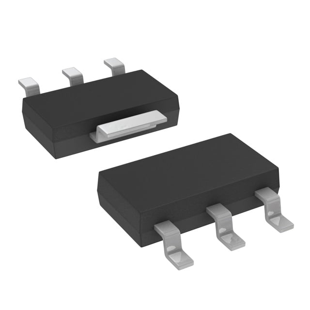
| 供应商器件封装 | SOT-223 |
| 其它名称 | LM2937IMP-8.0/NOPBTR |
| 包装 | 带卷 (TR) |
| 商标 | Texas Instruments |
| 回动电压—最大值 | 500 mV |
| 安装类型 | 表面贴装 |
| 安装风格 | SMD/SMT |
| 封装 | Reel |
| 封装/外壳 | TO-261-4,TO-261AA |
| 封装/箱体 | SOT-223-4 |
| 工作温度 | -40°C ~ 85°C |
| 工厂包装数量 | 1000 |
| 最大输入电压 | 26 V |
| 标准包装 | 1,000 |
| 电压-跌落(典型值) | 1V @ 500mA |
| 电压-输入 | 最高 26V |
| 电压-输出 | 8V |
| 电流-输出 | 400mA |
| 电流-限制(最小值) | - |
| 稳压器拓扑 | 正,固定式 |
| 稳压器数 | 1 |
| 系列 | LM2937 |
| 设计资源 | http://www.digikey.com/product-highlights/cn/zh/texas-instruments-webench-design-center/3176 |
| 输出电流 | 500 mA |


- 商务部:美国ITC正式对集成电路等产品启动337调查
- 曝三星4nm工艺存在良率问题 高通将骁龙8 Gen1或转产台积电
- 太阳诱电将投资9.5亿元在常州建新厂生产MLCC 预计2023年完工
- 英特尔发布欧洲新工厂建设计划 深化IDM 2.0 战略
- 台积电先进制程称霸业界 有大客户加持明年业绩稳了
- 达到5530亿美元!SIA预计今年全球半导体销售额将创下新高
- 英特尔拟将自动驾驶子公司Mobileye上市 估值或超500亿美元
- 三星加码芯片和SET,合并消费电子和移动部门,撤换高东真等 CEO
- 三星电子宣布重大人事变动 还合并消费电子和移动部门
- 海关总署:前11个月进口集成电路产品价值2.52万亿元 增长14.8%


PDF Datasheet 数据手册内容提取
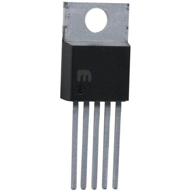
Product Sample & Technical Tools & Support & Folder Buy Documents Software Community LM2937 SNVS100F–MARCH2000–REVISEDJULY2014 LM2937 500-mA Low Dropout Regulator 1 Features 3 Description • FullySpecifiedforOperationOver−40°Cto125°C The LM2937 is a positive voltage regulator capable of 1 supplying up to 500 mA of load current. The use of a • OutputCurrentinExcessof500mA PNP power transistor provides a low dropout voltage • OutputTrimmedfor5%ToleranceUnderall characteristic. With a load current of 500 mA the OperatingConditions minimum input to output voltage differential required • TypicalDropoutVoltageof0.5VatFullRated for the output to remain in regulation is typically 0.5 V (1-V ensured maximum over the full operating LoadCurrent temperature range). Special circuitry has been • WideOutputCapacitorESRRange,upto3 Ω incorporated to minimize the quiescent current to • InternalShortCircuitandThermalOverload typically only 10 mA with a full 500-mA load current Protection when the input to output voltage differential is greater than3V. • ReverseBatteryProtection • 60-VInputTransientProtection The LM2937 requires an output bypass capacitor for stability. As with most low dropout regulators, the • MirrorImageInsertionProtection ESR of this capacitor remains a critical design parameter, but the LM2937 includes special 2 Applications compensation circuitry that relaxes ESR • Automotive requirements. The device is stable for all ESR below • IndustrialControl 3Ω.ThisallowstheuseoflowESRchipcapacitors. • Point-of-Loadregulation Ideallysuitedforautomotiveapplications,the LM2937 will protect itself and any load circuitry from reverse space battery connections, two-battery jumps, and up to 60- space V/−50-V load dump transients. Familiar regulator space features such as short circuit and thermal shutdown protectionarealsobuiltin. SimplifiedSchematic DeviceInformation(1) PART PACKAGE BODYSIZE(NOM) NUMBER TO-220(3) 14.986mmx10.66mm LM2937 SOT(4) 6.50mmx3.5mm TO-263(3) 10.18mmx8.41mm (1) For all available packages, see the orderable addendum at theendofthedatasheet. 1 An IMPORTANT NOTICE at the end of this data sheet addresses availability, warranty, changes, use in safety-critical applications, intellectualpropertymattersandotherimportantdisclaimers.PRODUCTIONDATA.
LM2937 SNVS100F–MARCH2000–REVISEDJULY2014 www.ti.com Table of Contents 1 Features.................................................................. 1 7.1 Overview.................................................................11 2 Applications........................................................... 1 7.2 FunctionalBlockDiagram.......................................11 3 Description............................................................. 1 7.3 FeatureDescription.................................................11 7.4 DeviceFunctionalModes........................................12 4 RevisionHistory..................................................... 2 8 ApplicationandImplementation........................ 13 5 PinConfigurationandFunctions......................... 3 8.1 ApplicationInformation............................................13 6 Specifications......................................................... 4 8.2 TypicalApplication .................................................13 6.1 AbsoluteMaximumRatings......................................4 9 PowerSupplyRecommendations...................... 17 6.2 HandlingRatings......................................................4 10 Layout................................................................... 18 6.3 RecommendedOperatingConditions.......................4 6.4 ThermalInformation..................................................4 10.1 LayoutGuidelines.................................................18 6.5 ElectricalCharacteristics:LM2937-5........................5 10.2 LayoutExample....................................................18 6.6 ElectricalCharacteristics:LM2937-8........................5 11 DeviceandDocumentationSupport................. 19 6.7 ElectricalCharacteristics:LM2937-10......................5 11.1 Trademarks...........................................................19 6.8 ElectricalCharacteristics:LM2937-12......................7 11.2 ElectrostaticDischargeCaution............................19 6.9 ElectricalCharacteristics:LM2937-15......................7 11.3 Glossary................................................................19 6.10 TypicalCharacteristics............................................8 12 Mechanical,Packaging,andOrderable Information........................................................... 19 7 DetailedDescription............................................ 11 4 Revision History NOTE:Pagenumbersforpreviousrevisionsmaydifferfrompagenumbersinthecurrentversion. ChangesfromRevisionE(June2013)toRevisionF Page • ChangedformattomeetnewTIstandards;addedDeviceInformationandHandlingRatingstables;updated connectiondrawings;renameFunctionalDescriptionandApplicationssections,reformatandaddnewinformation, addDevicesandDocumentationsection .............................................................................................................................. 1 2 SubmitDocumentationFeedback Copyright©2000–2014,TexasInstrumentsIncorporated ProductFolderLinks:LM2937
LM2937 www.ti.com SNVS100F–MARCH2000–REVISEDJULY2014 5 Pin Configuration and Functions TO-220PlasticPackage(NDE) 3 TopView INPUT 1 GND 2 OUTPUT 3 TAB SOT-223PlasticPackage(DCY) 4 TopView INPUT 1 4 GND 2 (TAB) OUTPUT 3 DDPAK/TO-263Surface-MountPackage(KTT) 3 TopView INPUT 1 T GND 2 A B OUTPUT 3 PinFunctions PIN I/O DESCRIPTION NAME NDE KTT DCY INPUT 1 1 1 I Unregulatedvoltageinput GND 2 2 2 — Ground Regulatedvoltageoutput.Thispinrequiresanoutputcapacitorto OUTPUT 3 3 3 O maintainstability.SeetheDetailedDesignProceduresectionforoutput capacitordetails. Thermalandgroundconnection.ConnecttheTABtoalargecopper areatoremoveheatfromthedevice.TheTABisinternallyconnected GND TAB TAB 4 — todevicepin2(GND).ConnecttheTABtoGNDorleavefloating.Do notconnecttheTABtoanypotentialotherthanGNDatdevicepin2. Copyright©2000–2014,TexasInstrumentsIncorporated SubmitDocumentationFeedback 3 ProductFolderLinks:LM2937
LM2937 SNVS100F–MARCH2000–REVISEDJULY2014 www.ti.com 6 Specifications 6.1 Absolute Maximum Ratings(1)(2) overoperatingfree-airtemperaturerange(unlessotherwisenoted) MIN MAX UNIT Continuous 26 Inputvoltage(V ) V IN Transient(t≤100ms) 60 Internalpowerdissipation(3) Internallylimited Maximumjunctiontemperature 150 °C (1) StressesbeyondthoselistedunderAbsoluteMaximumRatingsmaycausepermanentdamagetothedevice.Thesearestressratings only,whichdonotimplyfunctionaloperationofthedeviceattheseoranyotherconditionsbeyondthoseindicatedunderRecommended OperatingConditions.Exposuretoabsolute-maximum-ratedconditionsforextendedperiodsmayaffectdevicereliability. (2) IfMilitary/Aerospacespecifieddevicesarerequired,pleasecontacttheTexasInstrumentsSalesOffice/Distributorsforavailabilityand specifications. (3) ThemaximumallowablepowerdissipationatanyambienttemperatureisP =(125°C−T )/R ,where125isthemaximumjunction MAX A θJA temperatureforoperation,T istheambienttemperature,andR isthejunction-to-ambientthermalresistance.Ifthisdissipationis A θJA exceeded,thedietemperaturewillriseabove125°Candtheelectricalspecificationsdonotapply.Ifthedietemperaturerisesabove 150°C,theLM2937willgointothermalshutdown. 6.2 Handling Ratings MIN MAX UNIT T Storagetemperaturerange −65 150 °C stg Humanbodymodel(HBM),perANSI/ESDA/JEDECJS-001,all –2000 2000 V(ESD) Electrostaticdischarge pins(1) V (1) JEDECdocumentJEP155statesthat500-VHBMallowssafemanufacturingwithastandardESDcontrolprocess. 6.3 Recommended Operating Conditions(1) overoperatingfree-airtemperaturerange(unlessotherwisenoted) MIN NOM MAX UNIT LM2937ET(NDE),LM2937ES(KTT) −40 125 Junctiontemperature(T) (2) °C J LM2937IMP(DCY) −40 85 Inputvoltage(V ) V +1V 26 V IN OUT (1) StressesbeyondthoselistedunderAbsoluteMaximumRatingsmaycausepermanentdamagetothedevice.Thesearestressratings only,whichdonotimplyfunctionaloperationofthedeviceattheseoranyotherconditionsbeyondthoseindicatedunderRecommended OperatingConditions.Exposuretoabsolute-maximum-ratedconditionsforextendedperiodsmayaffectdevicereliability. (2) ThemaximumallowablepowerdissipationatanyambienttemperatureisP =(125°C−T )/R ,where125°Cisthemaximum MAX A θJA junctiontemperatureforoperation,T istheambienttemperature,andR isthejunction-to-ambientthermalresistance.Ifthis A θJA dissipationisexceeded,thedietemperaturewillriseabove125°Candtheelectricalspecificationsdonotapply.Ifthedietemperature risesabove150°C,theLM2937willgointothermalshutdown. 6.4 Thermal Information LM2937 THERMALMETRIC(1) NDE(2) KTT DCY UNIT 3PINS 3PINS 4PINS R Junction-to-ambientthermalresistance 77.9 41.8 58.3 θJA R Junction-to-case(top)thermalresistance 35.5 43.5 39.2 θJC(top) R Junction-to-boardthermalresistance 70.6 0.8 N/A θJB °C/W ψ Junction-to-topcharacterizationparameter 13 23.5 7 JT ψ Junction-to-boardcharacterizationparameter 70.6 10.3 1.6 JB R Junction-to-case(bottom)thermalresistance 1 22.5 22.5 θJC(bot) (1) Formoreinformationabouttraditionalandnewthermalmetrics,seetheICPackageThermalMetricsapplicationreport,SPRA953. (2) ThermalinformationfortheTO-220packageisforafree-standingpackageverticallymountedinthemiddleofaPCBwhichiscompliant totheJEDECHIGH-K2s2p(JESD51-7)specifications.Noadditionalheatsinkisattached.SeeHeatsinkingTO-220PackageParts sectionformoreinformation. 4 SubmitDocumentationFeedback Copyright©2000–2014,TexasInstrumentsIncorporated ProductFolderLinks:LM2937
LM2937 www.ti.com SNVS100F–MARCH2000–REVISEDJULY2014 6.5 Electrical Characteristics: LM2937-5 Unlessotherwisespecified:V =V )+5V;I =500mAfortheTO-220andDDPAK/TO-263packages;I IN OUT(NOM OUT(MAX) OUT(MAX) =400mAfortheSOT-223package;andC =10μF.Conditionsandtheassociatedminimumandmaximumlimitsapply OUT overtheRecommendedOperatingtemperaturerangeforthespecificpackage,unlessotherwisenoted. PARAMETER CONDITIONS MIN TYP MAX UNIT Outputvoltage T =T =25°C,5mA≤I ≤I 4.85 5 5.15 V A J OUT OUT(MAX) 5mA≤I ≤I 4.75 5 5.25 V OUT OUT(MAX) Lineregulation (V +2V)≤V ≤26V,I =5mA 15 50 mV OUT IN OUT Loadregulation 5mA≤I ≤I 5 50 mV OUT OUT(MAX) QuiescentCurrent (V +2V)≤V ≤26V,I =5mA 2 10 mA OUT IN OUT V =(V +5V),I =I 10 20 mA IN OUT OUT OUT(MAX) Outputnoisevoltage 10Hzto100kHz,I =5mA 150 μVrms OUT Long-termstability 1000Hrs. 20 mV Dropoutvoltage I =I 0.5 1 V OUT OUT(MAX) I =50mA 110 250 mV OUT Short-circuitcurrent 0.6 1 A Peaklinetransientvoltage tf<100ms,R =100Ω 60 75 V L Maximumoperationalinputvoltage 26 V ReverseDCinputvoltage V ≥−0.6V,R =100Ω –15 –30 V OUT L Reversetransientinputvoltage tr<1ms,R =100Ω –50 –75 V L 6.6 Electrical Characteristics: LM2937-8 Unlessotherwisespecified:V =V )+5V;I =500mAfortheTO-220andDDPAK/TO-263packages;I IN OUT(NOM OUT(MAX) OUT(MAX) =400mAfortheSOT-223package;andC =10μF.ConditionsandtheassociatedMinimumandMaximumlimitsapply OUT overtheRecommendedOperatingtemperaturerangeforthespecificpackage,unlessotherwisenoted. PARAMETER CONDITIONS MIN TYP MAX UNIT Outputvoltage T =T =25°C,5mA≤I ≤I 7.76 8 8.24 V A J OUT OUT(MAX) 5mA≤I ≤I 7.6 8 8.4 V OUT OUT(MAX) Lineregulation (V +2V)≤V ≤26V,I =5mA 24 80 mV OUT IN OUT Loadregulation 5mA≤I ≤I 8 80 mV OUT OUT(MAX) QuiescentCurrent (V +2V)≤V ≤26V,I =5mA 2 10 mA OUT IN OUT V =(V +5V),I =I 10 20 mA IN OUT OUT OUT(MAX) Outputnoisevoltage 10Hzto100kHz,I =5mA 240 μVrms OUT Long-termstability 1000Hrs. 32 mV Dropoutvoltage I =I 0.5 1 V OUT OUT(MAX) I =50mA 110 250 mV OUT Short-circuitcurrent 0.6 1 A Peaklinetransientvoltage tf<100ms,R =100Ω 60 75 V L Maximumoperationalinputvoltage 26 V ReverseDCinputvoltage V ≥−0.6V,R =100Ω –15 –30 V OUT L Reversetransientinputvoltage tr<1ms,R =100Ω –50 –75 V L 6.7 Electrical Characteristics: LM2937-10 Unlessotherwisespecified:V =V )+5V;I =500mAfortheTO-220andDDPAK/TO-263packages;I IN OUT(NOM OUT(MAX) OUT(MAX) =400mAfortheSOT-223package;andC =10μF.ConditionsandtheassociatedMinimumandMaximumlimitsapply OUT overtheRecommendedOperatingtemperaturerangeforthespecificpackage,unlessotherwisenoted. PARAMETER CONDITIONS MIN TYP MAX UNIT Outputvoltage T =T =25°C,5mA≤I ≤I 9.7 10 10.3 V A J OUT OUT(MAX) 5mA≤I ≤I 9.5 10 10.5 V OUT OUT(MAX) Lineregulation (V +2V)≤V ≤26V,I =5mA 30 100 mV OUT IN OUT Copyright©2000–2014,TexasInstrumentsIncorporated SubmitDocumentationFeedback 5 ProductFolderLinks:LM2937
LM2937 SNVS100F–MARCH2000–REVISEDJULY2014 www.ti.com Electrical Characteristics: LM2937-10 (continued) Unlessotherwisespecified:V =V )+5V;I =500mAfortheTO-220andDDPAK/TO-263packages;I IN OUT(NOM OUT(MAX) OUT(MAX) =400mAfortheSOT-223package;andC =10μF.ConditionsandtheassociatedMinimumandMaximumlimitsapply OUT overtheRecommendedOperatingtemperaturerangeforthespecificpackage,unlessotherwisenoted. PARAMETER CONDITIONS MIN TYP MAX UNIT Loadregulation 5mA≤I ≤I 10 100 mV OUT OUT(MAX) QuiescentCurrent (V +2V)≤V ≤26V,I =5mA 2 10 mA OUT IN OUT V =(V +5V),I =I 10 20 mA IN OUT OUT OUT(MAX) Outputnoisevoltage 10Hzto100kHz,I =5mA 300 μVrms OUT Long-termstability 1000Hrs. 40 mV Dropoutvoltage I =I 0.5 1 V OUT OUT(MAX) I =50mA 110 250 mV OUT Short-circuitcurrent 0.6 1 A Peaklinetransientvoltage tf<100ms,R =100Ω 60 75 V L Maximumoperationalinputvoltage 26 V ReverseDCinputvoltage V ≥−0.6V,R =100Ω –15 –30 V OUT L Reversetransientinputvoltage tr<1ms,R =100Ω –50 –75 V L 6 SubmitDocumentationFeedback Copyright©2000–2014,TexasInstrumentsIncorporated ProductFolderLinks:LM2937
LM2937 www.ti.com SNVS100F–MARCH2000–REVISEDJULY2014 6.8 Electrical Characteristics: LM2937-12 Unlessotherwisespecified:V =V )+5V;I =500mAfortheTO-220andDDPAK/TO-263packages;I IN OUT(NOM OUT(MAX) OUT(MAX) =400mAfortheSOT-223package;andC =10μF.ConditionsandtheassociatedMinimumandMaximumlimitsapply OUT overtheRecommendedOperatingtemperaturerangeforthespecificpackage,unlessotherwisenoted. PARAMETER CONDITIONS MIN TYP MAX UNIT Outputvoltage T =T =25°C,5mA≤I ≤I 11.64 12 12.36 V A J OUT OUT(MAX) 5mA≤I ≤I 11.4 12 12.6 V OUT OUT(MAX) Lineregulation (V +2V)≤V ≤26V,I =5mA 36 120 mV OUT IN OUT Loadregulation 5mA≤I ≤I 12 120 mV OUT OUT(MAX) QuiescentCurrent (V +2V)≤V ≤26V,I =5mA 2 10 mA OUT IN OUT V =(V +5V),I =I 10 20 mA IN OUT OUT OUT(MAX) Outputnoisevoltage 10Hzto100kHz,I =5mA 360 μVrms OUT Long-termstability 1000Hrs. 44 mV Dropoutvoltage I =I 0.5 1 V OUT OUT(MAX) I =50mA 110 250 mV OUT Short-circuitcurrent 0.6 1 A Peaklinetransientvoltage tf<100ms,R =100Ω 60 75 V L Maximumoperationalinputvoltage 26 V ReverseDCinputvoltage V ≥−0.6V,R =100Ω –15 –30 V OUT L Reversetransientinputvoltage tr<1ms,R =100Ω –50 –75 V L 6.9 Electrical Characteristics: LM2937-15 Unlessotherwisespecified:V =V )+5V;I =500mAfortheTO-220andDDPAK/TO-263packages;I IN OUT(NOM OUT(MAX) OUT(MAX) =400mAfortheSOT-223package;andC =10μF.ConditionsandtheassociatedMinimumandMaximumlimitsapply OUT overtheRecommendedOperatingtemperaturerangeforthespecificpackage,unlessotherwisenoted. PARAMETER CONDITIONS MIN TYP MAX UNIT Outputvoltage T =T =25°C,5mA≤I ≤I 14.55 15 15.45 V A J OUT OUT(MAX) 5mA≤I ≤I 14.25 15 15.75 V OUT OUT(MAX) Lineregulation (V +2V)≤V ≤26V,I =5mA 45 150 mV OUT IN OUT Loadregulation 5mA≤I ≤I 15 150 mV OUT OUT(MAX) QuiescentCurrent (V +2V)≤V ≤26V,I =5mA 2 10 mA OUT IN OUT V =(V +5V),I =I 10 20 mA IN OUT OUT OUT(MAX) Outputnoisevoltage 10Hzto100kHz,I =5mA 450 μVrms OUT Long-termstability 1000Hrs. 56 mV Dropoutvoltage I =I 0.5 1 V OUT OUT(MAX) I =50mA 110 250 mV OUT Short-circuitcurrent 0.6 1 A Peaklinetransientvoltage tf<100ms,R =100Ω 60 75 V L Maximumoperationalinputvoltage 26 V ReverseDCinputvoltage V ≥−0.6V,R =100Ω –15 –30 V OUT L Reversetransientinputvoltage tr<1ms,R =100Ω –50 –75 V L Copyright©2000–2014,TexasInstrumentsIncorporated SubmitDocumentationFeedback 7 ProductFolderLinks:LM2937
LM2937 SNVS100F–MARCH2000–REVISEDJULY2014 www.ti.com 6.10 Typical Characteristics Figure1.DropoutVoltagevs.OutputCurrent Figure2.DropoutVoltagevs.Temperature Figure3.OutputVoltagevs.Temperature Figure4.QuiescentCurrentvs.Temperature Figure5.QuiescentCurrentvs.InputVoltage Figure6.QuiescentCurrentvs.OutputCurrent 8 SubmitDocumentationFeedback Copyright©2000–2014,TexasInstrumentsIncorporated ProductFolderLinks:LM2937
LM2937 www.ti.com SNVS100F–MARCH2000–REVISEDJULY2014 Typical Characteristics (continued) Figure7.LineTransientResponse Figure8.LoadTransientResponse Figure9.RippleRejection Figure10.OutputImpedence Figure11.MaximumPowerDissipation(TO-220)1 Figure12.MaximumPowerDissipation(DDPAK/TO-263) 1.ThemaximumallowablepowerdissipationatanyambienttemperatureisP =(125°C−T )/R ,where125is MAX A θJA themaximumjunctiontemperatureforoperation,T istheambienttemperature,andR isthejunction-to-ambient A θJA thermalresistance.Ifthisdissipationisexceeded,thedietemperaturewillriseabove125°Candtheelectrical specificationsdonotapply.Ifthedietemperaturerisesabove150°C,theLM2937willgointothermalshutdown. Copyright©2000–2014,TexasInstrumentsIncorporated SubmitDocumentationFeedback 9 ProductFolderLinks:LM2937
LM2937 SNVS100F–MARCH2000–REVISEDJULY2014 www.ti.com Typical Characteristics (continued) Figure13.Low-VoltageBehavior Figure14.Low-VoltageBehavior Figure15.OutputatVoltageExtremes Figure16.OutputCapacitorESR Figure17.PeakOutputCurrent 10 SubmitDocumentationFeedback Copyright©2000–2014,TexasInstrumentsIncorporated ProductFolderLinks:LM2937
LM2937 www.ti.com SNVS100F–MARCH2000–REVISEDJULY2014 7 Detailed Description 7.1 Overview The LM2937 is a positive voltage regulator capable of supplying up to 500 mA of load current. The use of a PNP power transistor provides a low dropout voltage characteristic. With a load current of 500 mA the minimum input to output voltage differential required for the output to remain in regulation is typically 0.5 V (1 V ensured maximum over the full operating temperature range). Special circuitry has been incorporated to minimize the quiescent current to typically only 10 mA with a full 500-mA load current when the input to output voltage differentialisgreaterthan3V. 7.2 Functional Block Diagram INPUT OUTPUT PNP OVSD Thermal (§(cid:3)32V) Current Limit Shutdown + Bandgap Reference LM2937 GND 7.3 Feature Description 7.3.1 ThermalShutdown(TSD) The Thermal Shutdown circuitry of the LM2937 has been designed to protect the device against temporary thermal overload conditions. The TSD circuitry is not intended to replace proper heat-sinking. Continuously running the LM2937 device at thermal shutdown may degrade device reliability as the junction temperature will beexceedingtheabsolutemaximumjunctiontemperaturerating. 7.3.2 ShortCircuitCurrentLimit The output current limiting circuitry of the LM2937 has been designed to limit the output current in cases where theloadimpedanceisunusuallylow.Thisincludessituationswheretheoutputmaybeshorteddirectlytoground. Continuous operation of the LM2937 at the current limit will typically result in the LM2937 transitioning into ThermalShutdownmode. 7.3.3 OvervoltageShutdown(OVSD) Input voltages greater than typically 32 V will cause the LM2937 output to be disabled. When operating with the input voltage greater than the maximum recommended input voltage of 26 V the device performance is not ensured. Continuous operation with the input voltage greater than the maximum recommended input voltage is discouraged. Copyright©2000–2014,TexasInstrumentsIncorporated SubmitDocumentationFeedback 11 ProductFolderLinks:LM2937
LM2937 SNVS100F–MARCH2000–REVISEDJULY2014 www.ti.com 7.4 Device Functional Modes The LM2937 design does not include any undervoltage lock-out (UVLO), or enable functions. Generally, the output voltage will track the input voltage until the input voltage is greater than V + 1V. When the input OUT voltage is greater than V + 1V the LM2937 will be in linear operation, and the output voltage will be regulated; OUT however, the device will be sensitive to any small perturbation of the input voltage. Device dynamic performance isimprovedwhentheinputvoltageisatleast2Vgreaterthantheoutputvoltage. 12 SubmitDocumentationFeedback Copyright©2000–2014,TexasInstrumentsIncorporated ProductFolderLinks:LM2937
LM2937 www.ti.com SNVS100F–MARCH2000–REVISEDJULY2014 8 Application and Implementation 8.1 Application Information Figure 18 shows the typical application circuit for the LM2937. The output capacitor, C , must have a OUT capacitance value of at least 10 µF with an ESR of at least 10 mΩ, but no more than 3 Ω. The minimum capacitance value, and the ESR requirements apply across the entire expected operating ambient temperature range. 8.2 Typical Application Figure18. LM2937TypicalApplication *Requirediftheregulatorislocatedmorethan3inchesfromthepower-supply-filtercapacitors. **Requiredforstability.C mustbeatleast10µF(overfullexpectedoperatingtemperaturerange)and OUT locatedascloseaspossibletotheregulator.Theequivalentseriesresistance,ESR,ofthiscapacitormaybe ashighas3Ω. 8.2.1 DesignRequirements Forthisdesignexample,usetheparameterslistedinTable1: Table1.DesignParameters DESIGNPARAMETER EXAMPLEVALUE Outputvoltage 8V Inputvoltage 10Vto26V 5mAtoI (seeElectricalCharacteristics:LM2937-5,Electrical OUT(MAX) Characteristics:LM2937-8,ElectricalCharacteristics:LM2937-10, Outputcurrentrequirement ElectricalCharacteristics:LM2937-12,ElectricalCharacteristics: LM2937-15fordetails) Inputcapacitorvalue 0.1µF Outputcapacitorcapacitance 10µFminimum value OutputcapacitorESRvalue 0.01Ωto3Ω 8.2.2 DetailedDesignProcedure 8.2.2.1 ExternalCapacitors The output capacitor is critical to maintaining regulator stability, and must meet the required conditions for both EquivalentSeriesResistance(ESR)andminimumamountofcapacitance. MinimumCapacitance: The minimum output capacitance required to maintain stability is 10 μF. (This value may be increased without limit.)Largervaluesofoutputcapacitancewillgiveimprovedtransientresponse. ESRLimits: The ESR of the output capacitor will cause loop instability if it is too high or too low. The acceptable range of ESR plotted versus load current is shown in the graph below. It is essential that the output capacitor meet theserequirements,oroscillationscanresult. Copyright©2000–2014,TexasInstrumentsIncorporated SubmitDocumentationFeedback 13 ProductFolderLinks:LM2937
LM2937 SNVS100F–MARCH2000–REVISEDJULY2014 www.ti.com 8.2.2.2 OutputCapacitorESR Figure19. ESRLimits Itisimportanttonotethatformostcapacitors,ESRisspecifiedonlyatroomtemperature.However,thedesigner must ensure that the ESR will stay inside the limits shown over the entire operating temperature range for the design. Foraluminumelectrolyticcapacitors,ESRwillincreasebyabout30Xasthetemperatureisreducedfrom25°Cto −40°C.Thistypeofcapacitorisnotwell-suitedforlowtemperatureoperation. Solid tantalum capacitors have a more stable ESR over temperature, but are more expensive than aluminum electrolytics. A cost-effective approach sometimes used is to parallel an aluminum electrolytic with a solid Tantalum,withthetotalcapacitancesplitabout75/25%withtheAluminumbeingthelargervalue. If two capacitors are paralleled, the effective ESR is the parallel of the two individual values. The “flatter” ESR of theTantalumwillkeeptheeffectiveESRfromrisingasquicklyatlowtemperatures. 8.2.2.3 Heatsinking Aheatsinkmayberequireddependingonthemaximumpowerdissipationandmaximumambienttemperatureof the application. Under all possible operating conditions, the junction temperature must be within the range specifiedunderAbsoluteMaximumRatings. Todetermineifaheatsinkisrequired,thepowerdissipatedbytheregulator,P ,mustbecalculated. D Figure 20 below shows the voltages and currents which are present in the circuit, as well as the formula for calculatingthepowerdissipatedintheregulator: I =I +I IN L G P =(V −V )I +(V )I D IN OUT L IN G Figure20. PowerDissipationDiagram The next parameter which must be calculated is the maximum allowable temperature rise, T (max). This is R calculatedbyusingtheformula: T (max)=T(max)−T (max) R J A 14 SubmitDocumentationFeedback Copyright©2000–2014,TexasInstrumentsIncorporated ProductFolderLinks:LM2937
LM2937 www.ti.com SNVS100F–MARCH2000–REVISEDJULY2014 where • T (max)isthemaximumallowablejunctiontemperature,whichis125°CfortheTO-220andTO-263 J packages,and85°CfortheSOT-223package. • T (max)isthemaximumambienttemperaturewhichwillbeencounteredintheapplication. (1) A Using the calculated values for T (max) and P , the maximum allowable value for the junction-to-ambient R D thermalresistance,R ,cannowbefound: θJA R =T (max)/P (2) θJA R D NOTE IMPORTANT: If the maximum allowable value for R is found to be ≥ 53°C/W for the θJA TO-220 package, ≥ 80°C/W for the DDPAK/TO-263 package, or ≥ 174°C/W for the SOT- 223package,noheatsinkisneededsincethepackagealonewilldissipateenoughheatto satisfytheserequirements. IfthecalculatedvalueforR fallsbelowtheselimits,aheatsinkisrequired. θJA 8.2.2.4 HeatsinkingTO-220PackageParts TheTO-220canbeattachedtoatypicalheatsink,orsecuredtoacopperplaneonaPCboard.Ifacopperplane istobeused,thevaluesofR willbethesameasshowninthenextsectionfortheDDPAK/TO-263. θJA If a manufactured heatsink is to be selected, the value of heatsink-to-ambient thermal resistance, R , must first θHA becalculated: R =R −R −R θHA θJA θCH θJC where • R isdefinedasthethermalresistancefromthejunctiontothesurfaceofthecase.Avalueof3°C/Wcanbe θJC assumedforR forthiscalculation θJC • R isdefinedasthethermalresistancebetweenthecaseandthesurfaceoftheheatsink.ThevalueofR θCH θCH willvaryfromabout1.5°C/Wtoabout2.5°C/W(dependingonmethodofattachment,insulator,etc.).Ifthe exactvalueisunknown,2°C/WshouldbeassumedforR (3) θCH When a value for R is found using the equation shown, a heatsink must be selected that has a value that is θHA lessthanorequaltothisnumber. R is specified numerically by the heatsink manufacturer in the catalog, or shown in a curve that plots θHA temperaturerisevspowerdissipationfortheheatsink. 8.2.2.5 HeatsinkingDDPAK/TO-263andSOT-223PackageParts Both the DDPAK/TO-263 and SOT-223 packages use a copper plane on the PCB and the PCB itself as a heatsink.TooptimizetheheatsinkingabilityoftheplaneandPCB,solderthetabofthepackagetotheplane. Figure 21 shows for the DDPAK/TO-263 the measured values of R for different copper area sizes using a θJA typicalPCBwith1ouncecopperandnosoldermaskoverthecopperareausedforheatsinking. Copyright©2000–2014,TexasInstrumentsIncorporated SubmitDocumentationFeedback 15 ProductFolderLinks:LM2937
LM2937 SNVS100F–MARCH2000–REVISEDJULY2014 www.ti.com Figure21. R vs.Copper(1ounce)AreafortheDDPAK/TO-263Package θJA As shown in Figure 21, increasing the copper area beyond 1 square inch produces very little improvement. It should also be observed that the minimum value of R for the DDPAK/TO-263 package mounted to a PCB is θJA 32°C/W. As a design aid, Figure 22 shows the maximum allowable power dissipation compared to ambient temperature fortheDDPAK/TO-263device(assumingR is35°C/Wandthemaximumjunctiontemperatureis125°C). θJA Figure22. MaximumPowerDissipationvs.T fortheDDPAK/TO-263Package AMB Figure23andFigure24showinformationfortheSOT-223package.Figure24 assumesanR of74°C/Wfor1 θJA ouncecopperand51°C/Wfor2ouncecopperandamaximumjunctiontemperatureof85°C. 16 SubmitDocumentationFeedback Copyright©2000–2014,TexasInstrumentsIncorporated ProductFolderLinks:LM2937
LM2937 www.ti.com SNVS100F–MARCH2000–REVISEDJULY2014 Figure23.R vsCopper(2ounce)Areaforthe Figure24.MaximumPowerDissipationvsT for θJA AMB SOT-223Package theSOT-223Package 8.2.2.6 SOT-223SolderingRecommendations ItisnotrecommendedtousehandsolderingorwavesolderingtoattachthesmallSOT-223packagetoaprinted circuitboard.Theexcessivetemperaturesinvolvedmaycausepackagecracking. Either vapor phase or infrared reflow techniques are preferred soldering attachment methods for the SOT-223 package. 8.2.3 ApplicationCurves Figure25.OutputatVoltageExtremes Figure26.DropoutVoltagevs.Temperature 9 Power Supply Recommendations This device is designed to operate from an input supply voltage from at least V + 1 V up to a maximum of 26 OUT V. The input supply should be well regulated and free of spurious noise. To ensure that the LM2937 output voltage is well regulated the input supply should be at least V + 2 V. A capacitor at the INPUT pin may not be OUT specifically required if the bulk input supply filter capacitors are within three inches of the INPUT pin, but adding onewillnotbedetrimentaltooperation. Copyright©2000–2014,TexasInstrumentsIncorporated SubmitDocumentationFeedback 17 ProductFolderLinks:LM2937
LM2937 SNVS100F–MARCH2000–REVISEDJULY2014 www.ti.com 10 Layout 10.1 Layout Guidelines The dynamic performance of the LM2937 is dependent on the layout of the PCB. PCB layout practices that are adequate for typical LDO's may degrade the PSRR, noise, or transient performance of the LM2937. Best performance is achieved by placing C and C on the same side of the PCB as the LM2937, and as close as IN OUT is practical to the package. The ground connections for C and C should be back to the LM2937 ground pin IN OUT usingaswide,andasshort,ofacoppertraceasispractical. Connections using long trace lengths, narrow trace widths, and/or connections through vias should be avoided as these will add parasitic inductances and resistances that will give inferior performance, especially during transientconditions 10.2 Layout Example C C IN OUT INPUT 1 2 3 OUTPUT GND Figure27. LM2937SOT-223-4Layout 18 SubmitDocumentationFeedback Copyright©2000–2014,TexasInstrumentsIncorporated ProductFolderLinks:LM2937
LM2937 www.ti.com SNVS100F–MARCH2000–REVISEDJULY2014 11 Device and Documentation Support 11.1 Trademarks Alltrademarksarethepropertyoftheirrespectiveowners. 11.2 Electrostatic Discharge Caution Thesedeviceshavelimitedbuilt-inESDprotection.Theleadsshouldbeshortedtogetherorthedeviceplacedinconductivefoam duringstorageorhandlingtopreventelectrostaticdamagetotheMOSgates. 11.3 Glossary SLYZ022—TIGlossary. Thisglossarylistsandexplainsterms,acronyms,anddefinitions. 12 Mechanical, Packaging, and Orderable Information The following pages include mechanical, packaging, and orderable information. This information is the most current data available for the designated devices. This data is subject to change without notice and revision of thisdocument.Forbrowser-basedversionsofthisdatasheet,refertotheleft-handnavigation. Copyright©2000–2014,TexasInstrumentsIncorporated SubmitDocumentationFeedback 19 ProductFolderLinks:LM2937
PACKAGE OPTION ADDENDUM www.ti.com 6-Feb-2020 PACKAGING INFORMATION Orderable Device Status Package Type Package Pins Package Eco Plan Lead/Ball Finish MSL Peak Temp Op Temp (°C) Device Marking Samples (1) Drawing Qty (2) (6) (3) (4/5) LM2937ES-10/NOPB ACTIVE DDPAK/ KTT 3 45 Pb-Free (RoHS SN Level-3-245C-168 HR -40 to 125 LM2937ES TO-263 Exempt) -10 LM2937ES-12 NRND DDPAK/ KTT 3 45 TBD Call TI Call TI -40 to 125 LM2937ES TO-263 -12 LM2937ES-12/NOPB ACTIVE DDPAK/ KTT 3 45 Pb-Free (RoHS SN Level-3-245C-168 HR -40 to 125 LM2937ES TO-263 Exempt) -12 LM2937ES-15 NRND DDPAK/ KTT 3 45 TBD Call TI Call TI -40 to 125 LM2937ES TO-263 -15 LM2937ES-15/NOPB ACTIVE DDPAK/ KTT 3 45 Pb-Free (RoHS SN Level-3-245C-168 HR -40 to 125 LM2937ES TO-263 Exempt) -15 LM2937ES-2.5/NOPB ACTIVE DDPAK/ KTT 3 45 Pb-Free (RoHS SN Level-3-245C-168 HR -40 to 125 LM2937ES TO-263 Exempt) -2.5 LM2937ES-3.3 NRND DDPAK/ KTT 3 45 TBD Call TI Call TI -40 to 125 LM2937ES TO-263 -3.3 LM2937ES-3.3/NOPB ACTIVE DDPAK/ KTT 3 45 Pb-Free (RoHS SN Level-3-245C-168 HR -40 to 125 LM2937ES TO-263 Exempt) -3.3 LM2937ES-5.0 NRND DDPAK/ KTT 3 45 TBD Call TI Call TI -40 to 125 LM2937ES TO-263 -5.0 LM2937ES-5.0/NOPB ACTIVE DDPAK/ KTT 3 45 Pb-Free (RoHS SN Level-3-245C-168 HR -40 to 125 LM2937ES TO-263 Exempt) -5.0 LM2937ES-8.0/NOPB ACTIVE DDPAK/ KTT 3 45 Pb-Free (RoHS SN Level-3-245C-168 HR -40 to 125 LM2937ES TO-263 Exempt) -8.0 LM2937ESX-12/NOPB ACTIVE DDPAK/ KTT 3 500 Pb-Free (RoHS SN Level-3-245C-168 HR -40 to 125 LM2937ES TO-263 Exempt) -12 LM2937ESX-15/NOPB ACTIVE DDPAK/ KTT 3 500 Pb-Free (RoHS SN Level-3-245C-168 HR -40 to 125 LM2937ES TO-263 Exempt) -15 LM2937ESX-3.3 NRND DDPAK/ KTT 3 500 TBD Call TI Call TI -40 to 125 LM2937ES TO-263 -3.3 LM2937ESX-3.3/NOPB ACTIVE DDPAK/ KTT 3 500 Pb-Free (RoHS SN Level-3-245C-168 HR -40 to 125 LM2937ES TO-263 Exempt) -3.3 LM2937ESX-5.0 NRND DDPAK/ KTT 3 500 TBD Call TI Call TI -40 to 125 LM2937ES TO-263 -5.0 LM2937ESX-5.0/NOPB ACTIVE DDPAK/ KTT 3 500 Pb-Free (RoHS SN Level-3-245C-168 HR -40 to 125 LM2937ES TO-263 Exempt) -5.0 Addendum-Page 1
PACKAGE OPTION ADDENDUM www.ti.com 6-Feb-2020 Orderable Device Status Package Type Package Pins Package Eco Plan Lead/Ball Finish MSL Peak Temp Op Temp (°C) Device Marking Samples (1) Drawing Qty (2) (6) (3) (4/5) LM2937ESX-8.0/NOPB ACTIVE DDPAK/ KTT 3 500 Pb-Free (RoHS SN Level-3-245C-168 HR -40 to 125 LM2937ES TO-263 Exempt) -8.0 LM2937ET-10/NOPB ACTIVE TO-220 NDE 3 45 Green (RoHS SN Level-1-NA-UNLIM -40 to 125 LM2937ET & no Sb/Br) -10 LM2937ET-12 NRND TO-220 NDE 3 45 TBD Call TI Call TI -40 to 125 LM2937ET -12 LM2937ET-12/NOPB ACTIVE TO-220 NDE 3 45 Green (RoHS SN Level-1-NA-UNLIM -40 to 125 LM2937ET & no Sb/Br) -12 LM2937ET-15 NRND TO-220 NDE 3 45 TBD Call TI Call TI -40 to 125 LM2937ET -15 LM2937ET-15/NOPB ACTIVE TO-220 NDE 3 45 Green (RoHS SN Level-1-NA-UNLIM -40 to 125 LM2937ET & no Sb/Br) -15 LM2937ET-2.5/NOPB ACTIVE TO-220 NDE 3 45 Green (RoHS SN Level-1-NA-UNLIM -40 to 125 LM2937ET & no Sb/Br) -2.5 LM2937ET-3.3 NRND TO-220 NDE 3 45 TBD Call TI Call TI -40 to 125 LM2937ET -3.3 LM2937ET-3.3/NOPB ACTIVE TO-220 NDE 3 45 Green (RoHS SN Level-1-NA-UNLIM -40 to 125 LM2937ET & no Sb/Br) -3.3 LM2937ET-5.0 NRND TO-220 NDE 3 45 TBD Call TI Call TI -40 to 125 LM2937ET -5.0 LM2937ET-5.0/NOPB ACTIVE TO-220 NDE 3 45 Pb-Free (RoHS SN Level-1-NA-UNLIM -40 to 125 LM2937ET Exempt) -5.0 LM2937ET-8.0 NRND TO-220 NDE 3 45 TBD Call TI Call TI -40 to 125 LM2937ET -8.0 LM2937ET-8.0/NOPB ACTIVE TO-220 NDE 3 45 Green (RoHS SN Level-1-NA-UNLIM -40 to 125 LM2937ET & no Sb/Br) -8.0 LM2937IMP-10 NRND SOT-223 DCY 4 1000 TBD Call TI Call TI -40 to 85 L73B LM2937IMP-10/NOPB ACTIVE SOT-223 DCY 4 1000 Green (RoHS SN Level-1-260C-UNLIM -40 to 85 L73B & no Sb/Br) LM2937IMP-12 NRND SOT-223 DCY 4 1000 TBD Call TI Call TI -40 to 85 L74B LM2937IMP-12/NOPB ACTIVE SOT-223 DCY 4 1000 Green (RoHS SN Level-1-260C-UNLIM -40 to 85 L74B & no Sb/Br) LM2937IMP-2.5/NOPB ACTIVE SOT-223 DCY 4 1000 Green (RoHS SN Level-1-260C-UNLIM -40 to 85 L68B & no Sb/Br) LM2937IMP-3.3 NRND SOT-223 DCY 4 1000 TBD Call TI Call TI -40 to 85 L69B Addendum-Page 2
PACKAGE OPTION ADDENDUM www.ti.com 6-Feb-2020 Orderable Device Status Package Type Package Pins Package Eco Plan Lead/Ball Finish MSL Peak Temp Op Temp (°C) Device Marking Samples (1) Drawing Qty (2) (6) (3) (4/5) LM2937IMP-3.3/NOPB ACTIVE SOT-223 DCY 4 1000 Green (RoHS SN Level-1-260C-UNLIM -40 to 85 L69B & no Sb/Br) LM2937IMP-5.0 NRND SOT-223 DCY 4 1000 TBD Call TI Call TI -40 to 85 L71B LM2937IMP-5.0/NOPB ACTIVE SOT-223 DCY 4 1000 Green (RoHS SN Level-1-260C-UNLIM -40 to 85 L71B & no Sb/Br) LM2937IMP-8.0/NOPB ACTIVE SOT-223 DCY 4 1000 Green (RoHS SN Level-1-260C-UNLIM -40 to 85 L72B & no Sb/Br) LM2937IMPX-10/NOPB ACTIVE SOT-223 DCY 4 2000 Green (RoHS SN Level-1-260C-UNLIM -40 to 85 L73B & no Sb/Br) LM2937IMPX-12/NOPB ACTIVE SOT-223 DCY 4 2000 Green (RoHS SN Level-1-260C-UNLIM -40 to 85 L74B & no Sb/Br) LM2937IMPX-15/NOPB ACTIVE SOT-223 DCY 4 2000 Green (RoHS SN Level-1-260C-UNLIM -40 to 85 L75B & no Sb/Br) LM2937IMPX-2.5/NOPB ACTIVE SOT-223 DCY 4 2000 Green (RoHS SN Level-1-260C-UNLIM -40 to 85 L68B & no Sb/Br) LM2937IMPX-3.3 NRND SOT-223 DCY 4 2000 TBD Call TI Call TI -40 to 85 L69B LM2937IMPX-3.3/NOPB ACTIVE SOT-223 DCY 4 2000 Green (RoHS SN Level-1-260C-UNLIM -40 to 85 L69B & no Sb/Br) LM2937IMPX-5.0/NOPB ACTIVE SOT-223 DCY 4 2000 Green (RoHS SN Level-1-260C-UNLIM -40 to 85 L71B & no Sb/Br) LM2937IMPX-8.0 NRND SOT-223 DCY 4 2000 TBD Call TI Call TI -40 to 85 L72B LM2937IMPX-8.0/NOPB ACTIVE SOT-223 DCY 4 2000 Green (RoHS SN Level-1-260C-UNLIM -40 to 85 L72B & no Sb/Br) (1) The marketing status values are defined as follows: ACTIVE: Product device recommended for new designs. LIFEBUY: TI has announced that the device will be discontinued, and a lifetime-buy period is in effect. NRND: Not recommended for new designs. Device is in production to support existing customers, but TI does not recommend using this part in a new design. PREVIEW: Device has been announced but is not in production. Samples may or may not be available. OBSOLETE: TI has discontinued the production of the device. (2) RoHS: TI defines "RoHS" to mean semiconductor products that are compliant with the current EU RoHS requirements for all 10 RoHS substances, including the requirement that RoHS substance do not exceed 0.1% by weight in homogeneous materials. Where designed to be soldered at high temperatures, "RoHS" products are suitable for use in specified lead-free processes. TI may reference these types of products as "Pb-Free". RoHS Exempt: TI defines "RoHS Exempt" to mean products that contain lead but are compliant with EU RoHS pursuant to a specific EU RoHS exemption. Green: TI defines "Green" to mean the content of Chlorine (Cl) and Bromine (Br) based flame retardants meet JS709B low halogen requirements of <=1000ppm threshold. Antimony trioxide based flame retardants must also meet the <=1000ppm threshold requirement. Addendum-Page 3
PACKAGE OPTION ADDENDUM www.ti.com 6-Feb-2020 (3) MSL, Peak Temp. - The Moisture Sensitivity Level rating according to the JEDEC industry standard classifications, and peak solder temperature. (4) There may be additional marking, which relates to the logo, the lot trace code information, or the environmental category on the device. (5) Multiple Device Markings will be inside parentheses. Only one Device Marking contained in parentheses and separated by a "~" will appear on a device. If a line is indented then it is a continuation of the previous line and the two combined represent the entire Device Marking for that device. (6) Lead/Ball Finish - Orderable Devices may have multiple material finish options. Finish options are separated by a vertical ruled line. Lead/Ball Finish values may wrap to two lines if the finish value exceeds the maximum column width. Important Information and Disclaimer:The information provided on this page represents TI's knowledge and belief as of the date that it is provided. TI bases its knowledge and belief on information provided by third parties, and makes no representation or warranty as to the accuracy of such information. Efforts are underway to better integrate information from third parties. TI has taken and continues to take reasonable steps to provide representative and accurate information but may not have conducted destructive testing or chemical analysis on incoming materials and chemicals. TI and TI suppliers consider certain information to be proprietary, and thus CAS numbers and other limited information may not be available for release. In no event shall TI's liability arising out of such information exceed the total purchase price of the TI part(s) at issue in this document sold by TI to Customer on an annual basis. Addendum-Page 4
PACKAGE MATERIALS INFORMATION www.ti.com 17-Dec-2019 TAPE AND REEL INFORMATION *Alldimensionsarenominal Device Package Package Pins SPQ Reel Reel A0 B0 K0 P1 W Pin1 Type Drawing Diameter Width (mm) (mm) (mm) (mm) (mm) Quadrant (mm) W1(mm) LM2937ESX-12/NOPB DDPAK/ KTT 3 500 330.0 24.4 10.75 14.85 5.0 16.0 24.0 Q2 TO-263 LM2937ESX-15/NOPB DDPAK/ KTT 3 500 330.0 24.4 10.75 14.85 5.0 16.0 24.0 Q2 TO-263 LM2937ESX-3.3 DDPAK/ KTT 3 500 330.0 24.4 10.75 14.85 5.0 16.0 24.0 Q2 TO-263 LM2937ESX-3.3/NOPB DDPAK/ KTT 3 500 330.0 24.4 10.75 14.85 5.0 16.0 24.0 Q2 TO-263 LM2937ESX-5.0 DDPAK/ KTT 3 500 330.0 24.4 10.75 14.85 5.0 16.0 24.0 Q2 TO-263 LM2937ESX-5.0/NOPB DDPAK/ KTT 3 500 330.0 24.4 10.75 14.85 5.0 16.0 24.0 Q2 TO-263 LM2937ESX-8.0/NOPB DDPAK/ KTT 3 500 330.0 24.4 10.75 14.85 5.0 16.0 24.0 Q2 TO-263 LM2937IMP-10 SOT-223 DCY 4 1000 330.0 16.4 7.0 7.5 2.2 12.0 16.0 Q3 LM2937IMP-10/NOPB SOT-223 DCY 4 1000 330.0 16.4 7.0 7.5 2.2 12.0 16.0 Q3 LM2937IMP-12 SOT-223 DCY 4 1000 330.0 16.4 7.0 7.5 2.2 12.0 16.0 Q3 LM2937IMP-12/NOPB SOT-223 DCY 4 1000 330.0 16.4 7.0 7.5 2.2 12.0 16.0 Q3 LM2937IMP-2.5/NOPB SOT-223 DCY 4 1000 330.0 16.4 7.0 7.5 2.2 12.0 16.0 Q3 LM2937IMP-3.3 SOT-223 DCY 4 1000 330.0 16.4 7.0 7.5 2.2 12.0 16.0 Q3 PackMaterials-Page1
PACKAGE MATERIALS INFORMATION www.ti.com 17-Dec-2019 Device Package Package Pins SPQ Reel Reel A0 B0 K0 P1 W Pin1 Type Drawing Diameter Width (mm) (mm) (mm) (mm) (mm) Quadrant (mm) W1(mm) LM2937IMP-3.3/NOPB SOT-223 DCY 4 1000 330.0 16.4 7.0 7.5 2.2 12.0 16.0 Q3 LM2937IMP-5.0 SOT-223 DCY 4 1000 330.0 16.4 7.0 7.5 2.2 12.0 16.0 Q3 LM2937IMP-5.0/NOPB SOT-223 DCY 4 1000 330.0 16.4 7.0 7.5 2.2 12.0 16.0 Q3 LM2937IMP-8.0/NOPB SOT-223 DCY 4 1000 330.0 16.4 7.0 7.5 2.2 12.0 16.0 Q3 LM2937IMPX-10/NOPB SOT-223 DCY 4 2000 330.0 16.4 7.0 7.5 2.2 12.0 16.0 Q3 LM2937IMPX-12/NOPB SOT-223 DCY 4 2000 330.0 16.4 7.0 7.5 2.2 12.0 16.0 Q3 LM2937IMPX-15/NOPB SOT-223 DCY 4 2000 330.0 16.4 7.0 7.5 2.2 12.0 16.0 Q3 LM2937IMPX-2.5/NOPB SOT-223 DCY 4 2000 330.0 16.4 7.0 7.5 2.2 12.0 16.0 Q3 LM2937IMPX-3.3 SOT-223 DCY 4 2000 330.0 16.4 7.0 7.5 2.2 12.0 16.0 Q3 LM2937IMPX-3.3/NOPB SOT-223 DCY 4 2000 330.0 16.4 7.0 7.5 2.2 12.0 16.0 Q3 LM2937IMPX-5.0/NOPB SOT-223 DCY 4 2000 330.0 16.4 7.0 7.5 2.2 12.0 16.0 Q3 LM2937IMPX-8.0 SOT-223 DCY 4 2000 330.0 16.4 7.0 7.5 2.2 12.0 16.0 Q3 LM2937IMPX-8.0/NOPB SOT-223 DCY 4 2000 330.0 16.4 7.0 7.5 2.2 12.0 16.0 Q3 *Alldimensionsarenominal Device PackageType PackageDrawing Pins SPQ Length(mm) Width(mm) Height(mm) LM2937ESX-12/NOPB DDPAK/TO-263 KTT 3 500 367.0 367.0 45.0 LM2937ESX-15/NOPB DDPAK/TO-263 KTT 3 500 367.0 367.0 45.0 LM2937ESX-3.3 DDPAK/TO-263 KTT 3 500 367.0 367.0 45.0 LM2937ESX-3.3/NOPB DDPAK/TO-263 KTT 3 500 367.0 367.0 45.0 PackMaterials-Page2
PACKAGE MATERIALS INFORMATION www.ti.com 17-Dec-2019 Device PackageType PackageDrawing Pins SPQ Length(mm) Width(mm) Height(mm) LM2937ESX-5.0 DDPAK/TO-263 KTT 3 500 367.0 367.0 45.0 LM2937ESX-5.0/NOPB DDPAK/TO-263 KTT 3 500 367.0 367.0 45.0 LM2937ESX-8.0/NOPB DDPAK/TO-263 KTT 3 500 367.0 367.0 45.0 LM2937IMP-10 SOT-223 DCY 4 1000 367.0 367.0 35.0 LM2937IMP-10/NOPB SOT-223 DCY 4 1000 367.0 367.0 35.0 LM2937IMP-12 SOT-223 DCY 4 1000 367.0 367.0 35.0 LM2937IMP-12/NOPB SOT-223 DCY 4 1000 367.0 367.0 35.0 LM2937IMP-2.5/NOPB SOT-223 DCY 4 1000 367.0 367.0 35.0 LM2937IMP-3.3 SOT-223 DCY 4 1000 367.0 367.0 35.0 LM2937IMP-3.3/NOPB SOT-223 DCY 4 1000 367.0 367.0 35.0 LM2937IMP-5.0 SOT-223 DCY 4 1000 367.0 367.0 35.0 LM2937IMP-5.0/NOPB SOT-223 DCY 4 1000 367.0 367.0 35.0 LM2937IMP-8.0/NOPB SOT-223 DCY 4 1000 367.0 367.0 35.0 LM2937IMPX-10/NOPB SOT-223 DCY 4 2000 367.0 367.0 35.0 LM2937IMPX-12/NOPB SOT-223 DCY 4 2000 367.0 367.0 35.0 LM2937IMPX-15/NOPB SOT-223 DCY 4 2000 367.0 367.0 35.0 LM2937IMPX-2.5/NOPB SOT-223 DCY 4 2000 367.0 367.0 35.0 LM2937IMPX-3.3 SOT-223 DCY 4 2000 367.0 367.0 35.0 LM2937IMPX-3.3/NOPB SOT-223 DCY 4 2000 367.0 367.0 35.0 LM2937IMPX-5.0/NOPB SOT-223 DCY 4 2000 367.0 367.0 35.0 LM2937IMPX-8.0 SOT-223 DCY 4 2000 367.0 367.0 35.0 LM2937IMPX-8.0/NOPB SOT-223 DCY 4 2000 367.0 367.0 35.0 PackMaterials-Page3
MECHANICAL DATA NDE0003B www.ti.com
MECHANICAL DATA KTT0003B TS3B (Rev F) BOTTOM SIDE OF PACKAGE www.ti.com
MECHANICAL DATA MPDS094A – APRIL 2001 – REVISED JUNE 2002 DCY (R-PDSO-G4) PLASTIC SMALL-OUTLINE 6,70 (0.264) 6,30 (0.248) 3,10 (0.122) 2,90 (0.114) 4 0,10 (0.004) M 7,30 (0.287) 3,70 (0.146) 6,70 (0.264) 3,30 (0.130) Gauge Plane 1 2 3 0,84 (0.033) 0°–10° 0,25 (0.010) 2,30 (0.091) 0,66 (0.026) 0,10 (0.004) M 4,60 (0.181) 0,75 (0.030) MIN 1,70 (0.067) 1,80 (0.071) MAX 1,50 (0.059) 0,35 (0.014) 0,23 (0.009) Seating Plane 0,10 (0.0040) 0,08 (0.003) 0,02 (0.0008) 4202506/B 06/2002 NOTES: A. All linear dimensions are in millimeters (inches). B. This drawing is subject to change without notice. C. Body dimensions do not include mold flash or protrusion. D. Falls within JEDEC TO-261 Variation AA. • POST OFFICE BOX 655303 DALLAS, TEXAS 75265
None
IMPORTANTNOTICEANDDISCLAIMER TI PROVIDES TECHNICAL AND RELIABILITY DATA (INCLUDING DATASHEETS), DESIGN RESOURCES (INCLUDING REFERENCE DESIGNS), APPLICATION OR OTHER DESIGN ADVICE, WEB TOOLS, SAFETY INFORMATION, AND OTHER RESOURCES “AS IS” AND WITH ALL FAULTS, AND DISCLAIMS ALL WARRANTIES, EXPRESS AND IMPLIED, INCLUDING WITHOUT LIMITATION ANY IMPLIED WARRANTIES OF MERCHANTABILITY, FITNESS FOR A PARTICULAR PURPOSE OR NON-INFRINGEMENT OF THIRD PARTY INTELLECTUAL PROPERTY RIGHTS. These resources are intended for skilled developers designing with TI products. You are solely responsible for (1) selecting the appropriate TI products for your application, (2) designing, validating and testing your application, and (3) ensuring your application meets applicable standards, and any other safety, security, or other requirements. These resources are subject to change without notice. TI grants you permission to use these resources only for development of an application that uses the TI products described in the resource. Other reproduction and display of these resources is prohibited. No license is granted to any other TI intellectual property right or to any third party intellectual property right. TI disclaims responsibility for, and you will fully indemnify TI and its representatives against, any claims, damages, costs, losses, and liabilities arising out of your use of these resources. TI’s products are provided subject to TI’s Terms of Sale (www.ti.com/legal/termsofsale.html) or other applicable terms available either on ti.com or provided in conjunction with such TI products. TI’s provision of these resources does not expand or otherwise alter TI’s applicable warranties or warranty disclaimers for TI products. Mailing Address: Texas Instruments, Post Office Box 655303, Dallas, Texas 75265 Copyright © 2020, Texas Instruments Incorporated