ICGOO在线商城 > 集成电路(IC) > PMIC - 稳压器 - 线性 > TLV1117LV18DCYR

 Datasheet下载
- 型号: TLV1117LV18DCYR
- 制造商: Texas Instruments
- 库位|库存: xxxx|xxxx
- 要求:
| 数量阶梯 | 香港交货 | 国内含税 |
| +xxxx | $xxxx | ¥xxxx |
查看当月历史价格
查看今年历史价格
TLV1117LV18DCYR产品简介:
ICGOO电子元器件商城为您提供TLV1117LV18DCYR由Texas Instruments设计生产,在icgoo商城现货销售,并且可以通过原厂、代理商等渠道进行代购。 TLV1117LV18DCYR价格参考。Texas InstrumentsTLV1117LV18DCYR封装/规格:PMIC - 稳压器 - 线性, Linear Voltage Regulator IC Positive Fixed 1 Output 1.8V 1A SOT-223-4。您可以下载TLV1117LV18DCYR参考资料、Datasheet数据手册功能说明书,资料中有TLV1117LV18DCYR 详细功能的应用电路图电压和使用方法及教程。
TLV1117LV18DCYR 是 Texas Instruments(德州仪器)生产的一款低功耗、低压差线性稳压器(LDO),属于 PMIC(电源管理集成电路)中的线性稳压器类别。其主要应用场景如下:

 1. 便携式电子设备
   - TLV1117LV18DCYR 的低功耗特性和小封装尺寸使其非常适合用于电池供电的便携式设备,如:
     - 智能手表和可穿戴设备
     - 移动医疗设备(如脉搏血氧仪、血糖仪)
     - 遥控器和手持终端
   - 其输出电压为固定的 1.8V,能够为微控制器、传感器和其他低功耗组件提供稳定的电源。

 2. 嵌入式系统
   - 在嵌入式系统中,该器件可用于为 MCU(微控制单元)、DSP(数字信号处理器)或其他低功耗逻辑电路供电。
   - 常见应用包括:
     - 工业自动化模块
     - 数据采集系统
     - 物联网(IoT)节点

 3. 通信设备
   - TLV1117LV18DCYR 可为通信模块中的射频(RF)前端、基带处理器以及其他关键组件提供干净的电源,减少噪声干扰。
   - 应用场景包括:
     - 蓝牙模块
     - Wi-Fi 模块
     - GPS 接收器

 4. 消费类电子产品
   - 该稳压器适用于需要稳定低压电源的各种消费类电子产品,例如:
     - 数码相机
     - 音频播放器
     - 游戏控制器

 5. 汽车电子
   - 尽管 TLV1117LV18DCYR 不是专门设计用于汽车环境,但在某些非关键的车载应用中(如娱乐系统或传感器接口),它也可以发挥作用。

 6. 传感器和数据采集
   - 由于其低噪声特性,该器件适合为精密传感器和数据采集系统供电,确保测量结果的准确性。
   - 应用包括温度传感器、压力传感器和加速度计等。

 总结
TLV1117LV18DCYR 凭借其低静态电流、小封装和固定 1.8V 输出的特点,广泛应用于对功耗敏感且需要稳定低压电源的场景中。无论是便携式设备还是嵌入式系统,它都能提供可靠且高效的电源解决方案。
| 参数 | 数值 |
| 产品目录 | 集成电路 (IC)半导体 |
| 描述 | IC REG LDO 1.8V 1A SOT223低压差稳压器 1A,Pos Fix Vltg LDO Linear Reg |
| 产品分类 | |
| 品牌 | Texas Instruments |
| 产品手册 | |
| 产品图片 |
|
| rohs | 符合RoHS无铅 / 符合限制有害物质指令(RoHS)规范要求 |
| 产品系列 | 电源管理 IC,低压差稳压器,Texas Instruments TLV1117LV18DCYR- |
| 数据手册 | |
| 产品型号 | TLV1117LV18DCYR |
| PCN设计/规格 | |
| 产品种类 | 低压差稳压器 |
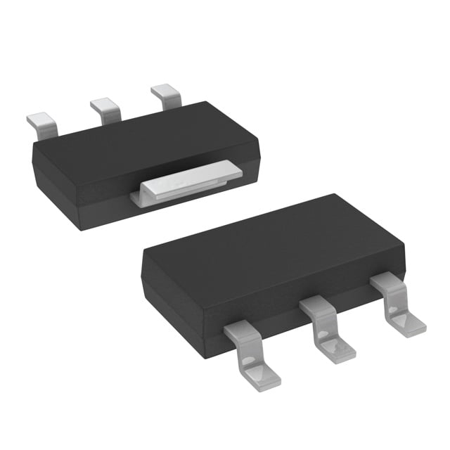
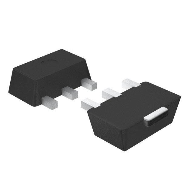
| 供应商器件封装 | SOT-223 |
| 其它名称 | 296-28777-6 |
| 包装 | Digi-Reel® |
| 商标 | Texas Instruments |
| 安装类型 | 表面贴装 |
| 安装风格 | SMD/SMT |
| 封装 | Reel |
| 封装/外壳 | TO-261-4,TO-261AA |
| 封装/箱体 | SOT-223-4 |
| 工作温度 | -40°C ~ 125°C |
| 工厂包装数量 | 2500 |
| 最大工作温度 | + 125 C |
| 最大输入电压 | 6 V |
| 最小工作温度 | - 40 C |
| 标准包装 | 1 |
| 电压-跌落(典型值) | 0.57V @ 1A |
| 电压-输入 | 2 V ~ 5.5 V |
| 电压-输出 | 1.8V |
| 电压调节准确度 | 1.5 % |
| 电流-输出 | 1A |
| 电流-限制(最小值) | 1.1A |
| 稳压器拓扑 | 正,固定式 |
| 稳压器数 | 1 |
| 系列 | TLV1117LV18 |
| 输出电流 | 80 mA |
| 输出类型 | Fixed |


- 商务部:美国ITC正式对集成电路等产品启动337调查
- 曝三星4nm工艺存在良率问题 高通将骁龙8 Gen1或转产台积电
- 太阳诱电将投资9.5亿元在常州建新厂生产MLCC 预计2023年完工
- 英特尔发布欧洲新工厂建设计划 深化IDM 2.0 战略
- 台积电先进制程称霸业界 有大客户加持明年业绩稳了
- 达到5530亿美元!SIA预计今年全球半导体销售额将创下新高
- 英特尔拟将自动驾驶子公司Mobileye上市 估值或超500亿美元
- 三星加码芯片和SET,合并消费电子和移动部门,撤换高东真等 CEO
- 三星电子宣布重大人事变动 还合并消费电子和移动部门
- 海关总署:前11个月进口集成电路产品价值2.52万亿元 增长14.8%


PDF Datasheet 数据手册内容提取
Product Sample & Technical Tools & Support & Folder Buy Documents Software Community TLV1117LV SBVS160B–MAY2011–REVISEDFEBRUARY2015 TLV1117LV 1-A, Positive Fixed-Voltage, Low-Dropout Regulator 1 Features 3 Description • 1.5%TypicalAccuracy The TLV1117LV series of low-dropout (LDO) linear 1 regulators is a low input voltage version of the • LowI :100μA(Maximum) Q popularTLV1117voltageregulator. – 500TimesLowerThanStandard1117 The TLV1117LV is an extremely low-power device Devices that consumes 500 times lower quiescent current • V :2Vto5.5V IN than traditional 1117 voltage regulators, making the – AbsoluteMaximumV =6V device suitable for applications that mandate very low IN standby current. The TLV1117LV family of LDOs is • StableWith0-mAOutputCurrent also stable with 0 mA of load current; there is no • LowDropout:455mVat1AforV =3.3V OUT minimum load requirement, making the device an • HighPSRR:65dBat1kHz ideal choice for applications where the regulator must • MinimumEnsuredCurrentLimit:1.1A power very small loads during standby in addition to large currents on the order of 1 A during normal • StableWithCost-EffectiveCeramicCapacitors: operation. The TLV1117LV offers excellent line and – With0-Ω ESR load transient performance, resulting in very small • TemperatureRange:–40°Cto125°C magnitude undershoots and overshoots of output voltage when the load current requirement changes • ThermalShutdownandOvercurrentProtection fromlessthan1mAtomorethan500mA. • AvailableinSOT-223Package A precision bandgap and error amplifier provides – SeeMechanical,Packaging,andOrderable 1.5% accuracy. A very high power-supply rejection Information attheendofthisdocumentfora ratio (PSRR) enables use of the device for post- completelistofavailablevoltageoptions. regulation after a switching regulator. Other valuable features include low output noise and low-dropout 2 Applications voltage. • SetTopBoxes The device is internally compensated to be stable • TVsandMonitors with 0-Ω equivalent series resistance (ESR) capacitors. These key advantages enable the use of • PCPeripherals,Notebooks,Motherboards cost-effective, small-size ceramic capacitors. Cost- • ModemsandOtherCommunicationProducts effective capacitors that have higher bias voltages • SwitchingPowerSupplyPost-Regulation andtemperaturederatingcanalsobeusedifdesired. The TLV1117LV series is available in a SOT-223 package. DeviceInformation(1) PARTNUMBER PACKAGE BODYSIZE(NOM) TLV1117LV SOT-223(4) 6.50mmx3.50mm (1) For all available packages, see the orderable addendum at theendofthedatasheet. TypicalApplicationCircuit INPUT OUTPUT CIN COUT 1 µF Device 1 µF GND 1 An IMPORTANT NOTICE at the end of this data sheet addresses availability, warranty, changes, use in safety-critical applications, intellectualpropertymattersandotherimportantdisclaimers.PRODUCTIONDATA.
TLV1117LV SBVS160B–MAY2011–REVISEDFEBRUARY2015 www.ti.com Table of Contents 1 Features.................................................................. 1 8.1 ApplicationInformation ..........................................13 2 Applications........................................................... 1 8.2 TypicalApplication..................................................13 3 Description............................................................. 1 8.3 Do'sandDon'ts.......................................................14 4 RevisionHistory..................................................... 2 9 PowerSupplyRecommendations...................... 14 5 PinConfigurationandFunctions......................... 3 10 Layout................................................................... 15 10.1 LayoutGuidelines.................................................15 6 Specifications......................................................... 4 10.2 LayoutExample....................................................15 6.1 AbsoluteMaximumRatings .....................................4 10.3 ThermalProtection................................................15 6.2 ESDRatings ............................................................4 10.4 PowerDissipation.................................................15 6.3 RecommendedOperatingConditions.......................4 11 DeviceandDocumentationSupport................. 16 6.4 ThermalInformation..................................................4 6.5 ElectricalCharacteristics...........................................5 11.1 DeviceSupport......................................................16 6.6 TypicalCharacteristics..............................................6 11.2 DocumentationSupport........................................16 11.3 RelatedLinks........................................................16 7 DetailedDescription............................................ 11 11.4 Trademarks...........................................................16 7.1 Overview.................................................................11 11.5 ElectrostaticDischargeCaution............................16 7.2 FunctionalBlockDiagram.......................................11 11.6 Glossary................................................................17 7.3 FeatureDescription.................................................11 12 Mechanical,Packaging,andOrderable 7.4 DeviceFunctionalModes........................................12 Information........................................................... 17 8 ApplicationandImplementation........................ 13 4 Revision History NOTE:Pagenumbersforpreviousrevisionsmaydifferfrompagenumbersinthecurrentversion. ChangesfromRevisionA(September2011)toRevisionB Page • AddedESDRatingstable,FeatureDescriptionsection,DeviceFunctionalModes,ApplicationandImplementation section,PowerSupplyRecommendationssection,Layoutsection,DeviceandDocumentationSupportsection,and Mechanical,Packaging,andOrderableInformationsection ................................................................................................. 1 • Replacedfront-pagefigure .................................................................................................................................................... 1 • DeletedDissipationRatingstable........................................................................................................................................... 4 ChangesfromOriginal(May,2011)toRevisionA Page • Changedfront-pagefigure..................................................................................................................................................... 1 2 SubmitDocumentationFeedback Copyright©2011–2015,TexasInstrumentsIncorporated ProductFolderLinks:TLV1117LV
TLV1117LV www.ti.com SBVS160B–MAY2011–REVISEDFEBRUARY2015 5 Pin Configuration and Functions DCYPackage 4Pins(SOT-223) TopView 3 INPUT T U P 2 OUTPUT T U O 1 GND PinFunctions PIN I/O DESCRIPTION NAME NO. Inputpin.SeeInputandOutputCapacitorRequirementsintheApplicationandImplementation IN 3 I sectionformoredetails. OUT 2,Tab O Regulatedoutputvoltagepin.SeeInputandOutputCapacitorRequirementsformoredetails. GND 1 — Groundpin. Copyright©2011–2015,TexasInstrumentsIncorporated SubmitDocumentationFeedback 3 ProductFolderLinks:TLV1117LV
TLV1117LV SBVS160B–MAY2011–REVISEDFEBRUARY2015 www.ti.com 6 Specifications 6.1 Absolute Maximum Ratings AtT =25°C(unlessotherwisenoted).AllvoltagesarewithrespecttoGND.(1) J MIN MAX UNIT V –0.3 6 V IN Voltage V –0.3 6 V OUT Current I Internallylimited OUT Outputshort-circuitduration Indefinite Continuoustotalpower P SeeThermalInformation dissipation DISS Operatingjunction,T –55 150 °C J Temperature Storage,T –55 150 °C stg (1) StressesbeyondthoselistedunderAbsoluteMaximumRatingsmaycausepermanentdamagetothedevice.Thesearestressratings only,andfunctionaloperationofthedeviceattheseoranyotherconditionsbeyondthoseindicatedunderRecommendedOperating Conditionsisnotimplied.Exposuretoabsolute-maximum-ratedconditionsforextendedperiodsmyaffectdevicereliability. 6.2 ESD Ratings VALUE UNIT Humanbodymodel(HBM),perANSI/ESDA/JEDECJS-001, allpins(1) ±2000 V Electrostaticdischarge V (ESD) Chargeddevicemodel(CDM),perJEDECspecification JESD22-C101,allpins(2) ±500 (1) JEDECdocumentJEP155statesthat500-VHBMallowssafemanufacturingwithastandardESDcontrolprocess. (2) JEDECdocumentJEP157statesthat250-VCDMallowssafemanufacturingwithastandardESDcontrolprocess. 6.3 Recommended Operating Conditions overoperatingfree-airtemperaturerange(unlessotherwisenoted) MIN NOM MAX UNIT V 2 5.5 V IN V 0 5.5 V OUT I 0 1 A OUT 6.4 Thermal Information TLV1117LV THERMALMETRIC(1) DCY(SOT-223) UNIT 4PINS R Junction-to-ambientthermalresistance 62.9 θJA θ Junction-to-case(top)thermalresistance 47.2 JCtop R Junction-to-boardthermalresistance 12 °C/W θJC(top) ψ Junction-to-topcharacterizationparameter 6.1 JT ψ Junction-to-boardcharacterizationparameter 11.9 JB (1) Formoreinformationabouttraditionalandnewthermalmetrics,seetheICPackageThermalMetricsapplicationreport,SPRA953. 4 SubmitDocumentationFeedback Copyright©2011–2015,TexasInstrumentsIncorporated ProductFolderLinks:TLV1117LV
TLV1117LV www.ti.com SBVS160B–MAY2011–REVISEDFEBRUARY2015 6.5 Electrical Characteristics AtV =V +1.5V;I =10mA,C =1.0μF,andT =25°C,unlessotherwisenoted. IN OUT(nom) OUT OUT A PARAMETER TESTCONDITIONS MIN TYP MAX UNIT V Inputvoltagerange 2 5.5 V IN V >2V –1.5% 1.5% OUT DCoutput V 1.5V≤V <2V –2% 2% OUT accuracy OUT 1.2V≤V <1.5V –40 40 mV OUT ΔV Lineregulation V +0.5V≤V ≤5.5V,I =10mA 1 5 mV OUT(ΔVIN) OUT(nom) IN OUT ΔV Loadregulation 0mA≤I ≤1A 1 35 mV OUT(ΔIOUT) OUT I =200mA 115 mV OUT I =500mA 285 mV OUT V <3.3V OUT I =800mA 455 mV OUT V Dropoutvoltage(1) VIN=0.98x IOUT=1A 570 800 mV DO VOUT(nom) IOUT=200mA 90 mV I =500mA 230 mV OUT V ≥3.3V OUT I =800mA 365 mV OUT I =1A 455 700 mV OUT I Outputcurrentlimit V =0.9×V 1.1 A CL OUT OUT(nom) I Quiescentcurrent I =0mA 50 100 µA Q OUT Power-supply V =3.3V,V =1.8V, PSRR IN OUT 65 dB rejectionratio I =500mA,f=100Hz OUT Outputnoise BW=10Hzto100kHz,V =2.8V,V =1.8V, V IN OUT 60 µV n voltage I =500mA RMS OUT t Startuptime(2) C =1.0µF,I =1A 100 µs STR OUT OUT Undervoltage UVLO V rising 1.95 V lockout IN Thermalshutdown Shutdown,temperatureincreasing 165 °C T SD temperature Reset,temperaturedecreasing 145 °C Operatingjunction T –40 125 °C J temperature (1) V ismeasuredfordeviceswithV =2.5VsothatV =2.45V. DO OUT(nom) IN (2) Startuptime=timefromwhenV assertstowhenoutputissustainedatavaluegreaterthanorequalto0.98×V . IN OUT(nom) Copyright©2011–2015,TexasInstrumentsIncorporated SubmitDocumentationFeedback 5 ProductFolderLinks:TLV1117LV
TLV1117LV SBVS160B–MAY2011–REVISEDFEBRUARY2015 www.ti.com 6.6 Typical Characteristics AtV =V +1.5V;I =10mA,C =1.0μF,andT =25°C,unlessotherwisenoted. IN OUT(nom) OUT OUT A 1.9 1.9 V = 1.8 V V = 1.8 V OUT OUT I = 10 mA I = 1 A OUT OUT 1.85 1.85 V) V) e ( e ( g g a a olt 1.8 olt 1.8 V V ut ut p p ut ut O O 1.75 +125°C 1.75 +85°C +85°C +25°C +25°C -40°C -40°C 1.7 1.7 2.3 2.7 3.1 3.5 3.9 4.3 4.7 5.1 5.5 3.3 3.5 3.7 3.9 4.1 4.3 4.5 4.7 4.9 5.1 5.3 5.5 Input Voltage (V) Input Voltage (V) Figure1.LineRegulation Figure2.LineRegulation 1.9 1200 VOUT= 1.8 V +85°C +25°C 1000 -40°C Voltage (V) 1.18.58 Voltage (mV) 860000 Output 1.75 +125°C Dropout 400 +85°C 200 +25°C -40°C 1.7 0 0 100 200 300 400 500 600 700 800 900 1000 2 2.5 3 3.5 4 4.5 Output Current (mA) Input Voltage (V) Figure3.LoadRegulation Figure4.DropoutVoltagevsInput 600 1.9 V = 1.8 V OUT 500 Voltage (mV) 430000 Voltage (V) 1.18.58 Dropout 200 +125°C Output 1.75 +85°C 100 +25°C 10 mA -40°C 500 mA 0 1.7 0 100 200 300 400 500 600 700 800 900 1000 -40 -25 -10 5 20 35 50 65 80 95 110 125 Output Current (mA) Temperature (°C) Figure5.DropoutVoltagevsOutput Figure6.OutputVoltagevsTemperature 6 SubmitDocumentationFeedback Copyright©2011–2015,TexasInstrumentsIncorporated ProductFolderLinks:TLV1117LV
TLV1117LV www.ti.com SBVS160B–MAY2011–REVISEDFEBRUARY2015 Typical Characteristics (continued) AtV =V +1.5V;I =10mA,C =1.0μF,andT =25°C,unlessotherwisenoted. IN OUT(nom) OUT OUT A 600 1.8 1.78 500 1.76 A) urrent (m 400 mit (mA) 11..7742 C 300 Li 1.7 ent ent 1.68 uiesc 200 +125°C Curr 1.66 Q 100 +85°C 1.64 +85°C +25°C 1.62 +25°C -40°C -40°C 0 1.6 0 100 200 300 400 500 600 700 800 900 1000 3.3 3.5 3.7 3.9 4.1 4.3 4.5 4.7 4.9 5.1 5.3 5.5 Output Current (mA) Input Voltage (V) Figure7.QuiescentCurrentvsLoad Figure8.CurrentLimitvsInputVoltage 90 90 I = 500 mA I = 500 mA B) 80 OUT B) 80 OUT d I = 150 mA d I = 150 mA atio ( 70 OIUOTUT= 30 mA atio ( 70 OIUOTUT= 30 mA R R n 60 n 60 o o cti 50 cti 50 e e ej ej R 40 R 40 y y ppl 30 ppl 30 u u S S er- 20 er- 20 w w Po 10 V -V = 3 V Po 10 V -V = 1.5 V IN OUT IN OUT 0 0 10 100 1 k 10 k 100 k 1 M 10 M 10 100 1 k 10 k 100 k 1 M 10 M Frequency (Hz) Frequency (Hz) Figure9.Power-SupplyRejectionRatiovsFrequency Figure10.Power-SupplyRejectionRatiovsFrequency 90 10 f = 50 Hz f = 120 Hz ction Ratio (dB) 87650000 f = 1 kHz f f= = 1 100 k0H kzHz m?nsity (V/)Hz 1 e e er-Supply Rej 432000 f = 10 MHz f = 1 MHz se Spectral D 0.00.11 w oi Po 10 V -V = 1.5 V N IN OUT 0 0.001 0 100 200 300 400 500 600 700 800 900 1000 10 100 1 k 10 k 100 k 1 M 10 M Output Current (mA) Frequency (Hz) Figure11.Power-SupplyRejectionRatiovsOutputCurrent Figure12.SpectralNoiseDensityvsFrequency Copyright©2011–2015,TexasInstrumentsIncorporated SubmitDocumentationFeedback 7 ProductFolderLinks:TLV1117LV
TLV1117LV SBVS160B–MAY2011–REVISEDFEBRUARY2015 www.ti.com Typical Characteristics (continued) AtV =V +1.5V;I =10mA,C =1.0μF,andT =25°C,unlessotherwisenoted. IN OUT(nom) OUT OUT A 500 mA V = 2.8 V 500 mA V = 2.8 V v IN v IN di di A/ A/ m m 00 200 mA IOUT 00 200 mA IOUT 2 2 V V OUT OUT v v di di V/ V/ m m 0 0 5 5 50ms/div 50ms/div Figure13.LoadTransientResponse200mAto500mA, Figure14.LoadTransientResponse200mAto500mA, C =1μF C =10μF OUT OUT V = 2.8 V div 500 mA IN div 500 mA A/ A/ m m 00 1 mA IOUT 00 1 mA IOUT 5 5 v v V/di VOUT V/di VOUT m m 0 0 5 5 50ms/div 50ms/div Figure15.LoadTransientResponse1mAto500mA, Figure16.LoadTransientResponse1mAto500mA, C =1μF C =10μF OUT OUT 1 A 1 A v v di di A/ A/ m m 00 200 mA IOUT 00 200 mA IOUT 5 5 v v V/di VOUT V/di VOUT m m 0 0 0 0 1 1 50ms/div 50ms/div Figure17.LoadTransientResponse200mAto1A, Figure18.LoadTransientResponse200mAto1A, C =1μF C =10μF OUT OUT 8 SubmitDocumentationFeedback Copyright©2011–2015,TexasInstrumentsIncorporated ProductFolderLinks:TLV1117LV
TLV1117LV www.ti.com SBVS160B–MAY2011–REVISEDFEBRUARY2015 Typical Characteristics (continued) AtV =V +1.5V;I =10mA,C =1.0μF,andT =25°C,unlessotherwisenoted. IN OUT(nom) OUT OUT A 1 A 1 A v v di di A/ A/ m m 00 1 mA IOUT 00 1 mA IOUT 5 5 v v V/di VOUT V/di VOUT m m 0 0 0 0 1 1 50ms/div 50ms/div Figure19.LoadTransientResponse1mAto1A, Figure20.LoadTransientResponse1mAto1A, C =1μF C =10μF OUT OUT 4.3 V 4.3 V v v di di 1 V/ 3.3 V VIN 1 V/ 3.3 V VIN v V v V di OUT di OUT V/ V/ m m 5 5 200ms/div 200ms/div Figure21.LineTransientResponseV =1.8V, Figure22.LineTransientResponseV =1.8V, OUT OUT I =10mA I =500mA OUT OUT 4.3 V 5.5 V v v di di 1 V/ 3.3 V VIN 1 V/ 3.3 V VIN v v V/di VOUT V/di VOUT m m 0 0 1 1 200ms/div 200ms/div Figure23.LineTransientResponseV =1.8V, Figure24.LineTransientResponseV =1.8V, OUT OUT I =1A I =10mA OUT OUT Copyright©2011–2015,TexasInstrumentsIncorporated SubmitDocumentationFeedback 9 ProductFolderLinks:TLV1117LV
TLV1117LV SBVS160B–MAY2011–REVISEDFEBRUARY2015 www.ti.com Typical Characteristics (continued) AtV =V +1.5V;I =10mA,C =1.0μF,andT =25°C,unlessotherwisenoted. IN OUT(nom) OUT OUT A 5.5 V 5.5 V v v di di 1 V/ 3.3 V VIN 1 V/ 3.3 V VIN v v V/di VOUT V/di VOUT m m 0 0 1 1 200ms/div 200ms/div Figure25.LineTransientResponseV =1.8V, Figure26.LineTransientResponseV =1.8V, OUT OUT I =500mA I =1A OUT OUT 10 SubmitDocumentationFeedback Copyright©2011–2015,TexasInstrumentsIncorporated ProductFolderLinks:TLV1117LV
TLV1117LV www.ti.com SBVS160B–MAY2011–REVISEDFEBRUARY2015 7 Detailed Description 7.1 Overview TheTLV1117LVfamilyofdevicesareaseriesoflowquiescentcurrent,highPSRRLDOscapableofhandlingup to 1 A of load current. These devices feature an integrated current limit, thermal shutdown, bandgap reference, andUVLOcircuitblocks. 7.2 Functional Block Diagram IN OUT Current Limit Thermal Shutdown UVLO Bandgap LOGIC TLV1117LV Series GND 7.3 Feature Description 7.3.1 InternalCurrentLimit The TLV1117LV internal current limit helps to protect the regulator during fault conditions. During current limit, theoutputsourcesafixedamountofcurrentthatislargelyindependentoftheoutputvoltage.Insuchacase,the output voltage is not regulated, and can be calculated by the formula: V = I × R . The PMOS pass OUT LIMIT LOAD transistor dissipates (V – V ) × I until thermal shutdown is triggered and the device turns off. As the IN OUT LIMIT device cools down, it is turned on by the internal thermal shutdown circuit. If the fault condition continues, the devicecyclesbetweencurrentlimitandthermalshutdown.SeetheThermalInformationsectionformoredetails The PMOS pass element in the TLV1117LV device has a built-in body diode that conducts current when the voltage at OUT exceeds the voltage at IN. This current is not limited; if extended reverse voltage operation is anticipated,externallimitingto5%oftheratedoutputcurrentisrecommended. 7.3.2 DropoutVoltage The TLV1117LV uses a PMOS pass transistor to achieve low dropout. When (V – V ) is less than the IN OUT dropout voltage (V ), the PMOS pass device is in the linear region of operation and the input-to-output DO resistance is the R of the PMOS pass element. V scales approximately with output current because the DS(ON) DO PMOSdevicebehavesasaresistorindropout. Aswithanylinearregulator,PSRRandtransientresponsearedegradedas(V –V )approachesdropout. IN OUT Copyright©2011–2015,TexasInstrumentsIncorporated SubmitDocumentationFeedback 11 ProductFolderLinks:TLV1117LV
TLV1117LV SBVS160B–MAY2011–REVISEDFEBRUARY2015 www.ti.com Feature Description (continued) 7.3.3 UndervoltageLockout The TLV1117LV uses an undervoltage lockout (UVLO) circuit keep the output shut off until internal circuitry operatingproperly. 7.4 Device Functional Modes 7.4.1 NormalOperation Thedeviceregulatestothenominaloutputvoltageunderthefollowingconditions: • Theinputvoltageisgreaterthanthenominaloutputvoltageaddedtothedropoutvoltage. • Theoutputcurrentislessthanthecurrentlimit. • Thedevicedietemperatureislowerthanthethermalshutdowntemperature. 7.4.2 DropoutOperation If the input voltage is lower than the nominal output voltage plus the specified dropout voltage, but all other conditions are met for normal operation, the device operates in dropout mode. In this condition, the output voltage is the same the input voltage minus the dropout voltage. The transient performance of the device is significantly degraded because the pass device is in a triode state and no longer controls the current through the LDO.Lineorloadtransientsindropoutmayresultinlargeoutputvoltagedeviations. Table1showstheconditionsthatleadtothedifferentmodesofoperation. Table1.DeviceFunctionalModeComparison PARAMETER OPERATINGMODE V I IN OUT Normalmode V >V +V I <I IN OUT(nom) DO OUT CL Dropoutmode V <V +V I <I IN OUT(nom) DO OUT CL 12 SubmitDocumentationFeedback Copyright©2011–2015,TexasInstrumentsIncorporated ProductFolderLinks:TLV1117LV
TLV1117LV www.ti.com SBVS160B–MAY2011–REVISEDFEBRUARY2015 8 Application and Implementation NOTE Information in the following applications sections is not part of the TI component specification, and TI does not warrant its accuracy or completeness. TI’s customers are responsible for determining suitability of components for their purposes. Customers should validateandtesttheirdesignimplementationtoconfirmsystemfunctionality. 8.1 Application Information The TLV1117LV is a low quiescent current linear regulator designed for high current applications. Unlike typical high current linear regulators, the TLV1117LV series consume significantly less quiescent current. These devices deliver excellent line and load transient performance. The device is low noise, and exhibits a very good PSRR. Asaresult,itisidealforhighcurrentapplicationsthatrequireverysensitivepower-supplyrails. This family of regulators offers both current limit and thermal protection. The operating junction temperature rangeofthedeviceis–40°Cto+125°C. 8.2 Typical Application Figure27showsatypicalapplicationcircuit. INPUT OUTPUT CIN COUT 1 µF Device 1 µF GND Figure27. TypicalApplicationCircuit 8.2.1 DesignRequirements Forthisdesignexample,usetheparameterslistedinTable2astheinputparameters. Table2.DesignParameters PARAMETER DESIGNREQUIREMENT InputVoltage 2.5Vto3.3V OutputVoltage 1.8V OutputCurrent 500mA 8.2.2 DetailedDesignProcedure 8.2.2.1 InputandOutputCapacitorRequirements For stability, 1.0-μF ceramic capacitors are required at the output. Higher-valued capacitors improve transient performance. TI recommends the X5R- and X7R-type ceramic capacitors because these capacitors have minimal variation in value and equivalent series resistance (ESR) over temperature. Unlike traditional linear regulators that need a minimum ESR for stability, the TLV1117LV series are ensured to be stable with no ESR. Therefore, cost-effective ceramic capacitors can be used with these devices. Effective output capacitance that takes bias, temperature, and aging effects into consideration must be greater than 0.5 μF to ensure stability of thedevice. Copyright©2011–2015,TexasInstrumentsIncorporated SubmitDocumentationFeedback 13 ProductFolderLinks:TLV1117LV
TLV1117LV SBVS160B–MAY2011–REVISEDFEBRUARY2015 www.ti.com Although an input capacitor is not required for stability, it is good analog design practice to connect a 0.1-μF to 1.0-μF, low-ESR capacitor across the IN pin and GND pin of the regulator. This capacitor counteracts reactive input sources and improves transient response, noise rejection, and ripple rejection. A higher-value capacitor may be necessary if large, fast rise-time load transients are anticipated, or if the device is not located physically close to the power source. If source impedance is greater than 2 Ω, a 0.1-μF, the input capacitor may also be necessarytoensurestability. 8.2.2.2 TransientResponse Aswithanyregulator,increasingthesizeoftheoutputcapacitorreducesovershootandundershootmagnitude. 8.2.3 ApplicationCurves 500 mA V = 2.8 V v IN di 200 mA/ 200 mA IOUT 1 V/div 34.3.3 V V VIN V OUT v mV/di V/div VOUT 50 5 m 50ms/div 200ms/div Figure28.LoadTransientResponse200mAto500mA, Figure29.LineTransientResponseV =1.8V,I = OUT OUT C =1μF 500mA OUT 8.3 Do's and Don'ts Placeinputandoutputcapacitorsasclosetothedeviceaspossible. Useaceramicoutputcapacitor. Donotuseanelectrolyticoutputcapacitor. Donotexceedthedeviceabsolutemaximumratings. 9 Power Supply Recommendations Connect a low output impedance power supply directly to the INPUT pin of the TLV1117LV. Inductive impedances between the input supply and the INPUT pin can create significant voltage excursions at the INPUT pinduringstartuporloadtransientevents. 14 SubmitDocumentationFeedback Copyright©2011–2015,TexasInstrumentsIncorporated ProductFolderLinks:TLV1117LV
TLV1117LV www.ti.com SBVS160B–MAY2011–REVISEDFEBRUARY2015 10 Layout 10.1 Layout Guidelines Input and output capacitors should be placed as close to the device pins as possible. To improve characteristic AC performance such as PSRR, output noise, and transient response, TI recommends designing the board with separate ground planes for V and V , with the ground plane connected only at the GND pin of the device. In IN OUT addition, the ground connection for the output capacitor should be connected directly to the GND pin of the device.HighervalueESRcapacitorsmaydegradePSRRperformance. 10.2 Layout Example OUTPUT Tab GND COUT CIN 1 2 3 GND INPUT Figure30. LayoutExample 10.3 Thermal Protection Thermal protection disables the output when the junction temperature rises to approximately 165°C, allowing the device to cool. When the junction temperature cools to approximately 145°C, the output circuitry is again enabled. Depending on power dissipation, thermal resistance, and ambient temperature, the thermal protection circuit may cycle on and off. This cycling limits the dissipation of the regulator, protecting it from damage as a resultofoverheating. Any tendency to activate the thermal protection circuit indicates excessive power dissipation or an inadequate heatsink. For reliable operation, junction temperature should be limited to 125°C maximum. To estimate the margin of safety in a complete design (including heatsink), increase the ambient temperature until the thermal protectionistriggered;useworst-caseloadsandsignalconditions. The internal protection circuitry of the TLV1117LV has been designed to protect against overload conditions. It was not intended to replace proper heatsinking. Continuously running the TLV1117LV into thermal shutdown degradesdevicereliability. 10.4 Power Dissipation The ability to remove heat from the die is different for each package type, presenting different considerations in the printed circuit board (PCB) layout. The PCB area around the device that is free of other components moves the heat from the device to the ambient air. Performance data for JEDEC low and high-K boards are given in the Thermal Information table. Using heavier copper increases the effectiveness in removing heat from the device. Theadditionofplatedthrough-holestoheat-dissipatinglayersalsoimprovesheatsinkeffectiveness. Powerdissipationdependsoninputvoltageandloadconditions.Powerdissipation(P )isequaltotheproductof D theoutputcurrentandthevoltagedropacrosstheoutputpasselement,asshowninEquation1: P = (V -V ) I D IN OUT OUT (1) Copyright©2011–2015,TexasInstrumentsIncorporated SubmitDocumentationFeedback 15 ProductFolderLinks:TLV1117LV
TLV1117LV SBVS160B–MAY2011–REVISEDFEBRUARY2015 www.ti.com 11 Device and Documentation Support 11.1 Device Support 11.1.1 DevelopmentSupport 11.1.1.1 EvaluationModule An evaluation module (EVM) is available to assist in the initial circuit performance evaluation using the TLV1117LV. The TLV1117LV33EVM-714 evaluation module (and related user's guide) can be requested at the TIwebsitethroughtheproductfoldersorpurchaseddirectlyfromtheTIeStore. 11.1.1.2 SpiceModels Computer simulation of circuit performance using SPICE is often useful when analyzing the performance of analog circuits and systems. A SPICE model for the TLV1117LV is available through the product folders under Tools& Software. 11.1.2 DeviceNomenclature Table3.AvailableOptions(1) PRODUCT V OUT xxisnominaloutputvoltage(forexample33=3.3V) TLV1117LVxxyyyz yyyisPackageDesignator zisPackageQuantity (1) Forthemostcurrentpackageandorderinginformation,seethePackageOptionAddendumattheendofthisdocument,orvisitthe deviceproductfolderatwww.ti.com. 11.2 Documentation Support 11.2.1 RelatedDocumentation • TLV1117LV33EVM-714EvaluationModuleUser'sGuide,SLVU449. 11.3 Related Links The table below lists quick access links. Categories include technical documents, support and community resources,toolsandsoftware,andquickaccesstosampleorbuy. Table4.RelatedLinks TECHNICAL TOOLS& SUPPORT& PARTS PRODUCTFOLDER SAMPLE&BUY DOCUMENTS SOFTWARE COMMUNITY TLV1117LV12 Clickhere Clickhere Clickhere Clickhere Clickhere TLV1117LV15 Clickhere Clickhere Clickhere Clickhere Clickhere TLV1117LV18 Clickhere Clickhere Clickhere Clickhere Clickhere TLV1117LV25 Clickhere Clickhere Clickhere Clickhere Clickhere TLV1117LV28 Clickhere Clickhere Clickhere Clickhere Clickhere TLV1117LV30 Clickhere Clickhere Clickhere Clickhere Clickhere TLV1117LV33 Clickhere Clickhere Clickhere Clickhere Clickhere 11.4 Trademarks Alltrademarksarethepropertyoftheirrespectiveowners. 11.5 Electrostatic Discharge Caution Thesedeviceshavelimitedbuilt-inESDprotection.Theleadsshouldbeshortedtogetherorthedeviceplacedinconductivefoam duringstorageorhandlingtopreventelectrostaticdamagetotheMOSgates. 16 SubmitDocumentationFeedback Copyright©2011–2015,TexasInstrumentsIncorporated ProductFolderLinks:TLV1117LV
TLV1117LV www.ti.com SBVS160B–MAY2011–REVISEDFEBRUARY2015 11.6 Glossary SLYZ022—TIGlossary. Thisglossarylistsandexplainsterms,acronyms,anddefinitions. 12 Mechanical, Packaging, and Orderable Information The following pages include mechanical, packaging, and orderable information. This information is the most current data available for the designated devices. This data is subject to change without notice and revision of thisdocument.Forbrowser-basedversionsofthisdatasheet,refertotheleft-handnavigation. Copyright©2011–2015,TexasInstrumentsIncorporated SubmitDocumentationFeedback 17 ProductFolderLinks:TLV1117LV
PACKAGE OPTION ADDENDUM www.ti.com 11-Feb-2015 PACKAGING INFORMATION Orderable Device Status Package Type Package Pins Package Eco Plan Lead/Ball Finish MSL Peak Temp Op Temp (°C) Device Marking Samples (1) Drawing Qty (2) (6) (3) (4/5) TLV1117LV12DCYR ACTIVE SOT-223 DCY 4 2500 Green (RoHS CU SN Level-1-260C-UNLIM -40 to 125 SI & no Sb/Br) TLV1117LV12DCYT ACTIVE SOT-223 DCY 4 250 Green (RoHS CU SN Level-1-260C-UNLIM -40 to 125 SI & no Sb/Br) TLV1117LV15DCYR ACTIVE SOT-223 DCY 4 2500 Green (RoHS CU SN Level-1-260C-UNLIM -40 to 125 VR & no Sb/Br) TLV1117LV15DCYT ACTIVE SOT-223 DCY 4 250 Green (RoHS CU SN Level-1-260C-UNLIM -40 to 125 VR & no Sb/Br) TLV1117LV18DCYR ACTIVE SOT-223 DCY 4 2500 Green (RoHS CU SN Level-1-260C-UNLIM -40 to 125 SH & no Sb/Br) TLV1117LV18DCYT ACTIVE SOT-223 DCY 4 250 Green (RoHS CU SN Level-1-260C-UNLIM -40 to 125 SH & no Sb/Br) TLV1117LV25DCYR ACTIVE SOT-223 DCY 4 2500 Green (RoHS CU SN Level-1-260C-UNLIM -40 to 125 VS & no Sb/Br) TLV1117LV25DCYT ACTIVE SOT-223 DCY 4 250 Green (RoHS CU SN Level-1-260C-UNLIM -40 to 125 VS & no Sb/Br) TLV1117LV28DCYR ACTIVE SOT-223 DCY 4 2500 Green (RoHS CU SN Level-1-260C-UNLIM -40 to 125 VT & no Sb/Br) TLV1117LV28DCYT ACTIVE SOT-223 DCY 4 250 Green (RoHS CU SN Level-1-260C-UNLIM -40 to 125 VT & no Sb/Br) TLV1117LV30DCYR ACTIVE SOT-223 DCY 4 2500 Green (RoHS CU SN Level-1-260C-UNLIM -40 to 125 VU & no Sb/Br) TLV1117LV30DCYT ACTIVE SOT-223 DCY 4 250 Green (RoHS CU SN Level-1-260C-UNLIM -40 to 125 VU & no Sb/Br) TLV1117LV33DCYR ACTIVE SOT-223 DCY 4 2500 Green (RoHS CU SN Level-1-260C-UNLIM -40 to 125 TJ & no Sb/Br) TLV1117LV33DCYT ACTIVE SOT-223 DCY 4 250 Green (RoHS CU SN Level-1-260C-UNLIM -40 to 125 TJ & no Sb/Br) (1) The marketing status values are defined as follows: ACTIVE: Product device recommended for new designs. LIFEBUY: TI has announced that the device will be discontinued, and a lifetime-buy period is in effect. NRND: Not recommended for new designs. Device is in production to support existing customers, but TI does not recommend using this part in a new design. PREVIEW: Device has been announced but is not in production. Samples may or may not be available. OBSOLETE: TI has discontinued the production of the device. Addendum-Page 1
PACKAGE OPTION ADDENDUM www.ti.com 11-Feb-2015 (2) Eco Plan - The planned eco-friendly classification: Pb-Free (RoHS), Pb-Free (RoHS Exempt), or Green (RoHS & no Sb/Br) - please check http://www.ti.com/productcontent for the latest availability information and additional product content details. TBD: The Pb-Free/Green conversion plan has not been defined. Pb-Free (RoHS): TI's terms "Lead-Free" or "Pb-Free" mean semiconductor products that are compatible with the current RoHS requirements for all 6 substances, including the requirement that lead not exceed 0.1% by weight in homogeneous materials. Where designed to be soldered at high temperatures, TI Pb-Free products are suitable for use in specified lead-free processes. Pb-Free (RoHS Exempt): This component has a RoHS exemption for either 1) lead-based flip-chip solder bumps used between the die and package, or 2) lead-based die adhesive used between the die and leadframe. The component is otherwise considered Pb-Free (RoHS compatible) as defined above. Green (RoHS & no Sb/Br): TI defines "Green" to mean Pb-Free (RoHS compatible), and free of Bromine (Br) and Antimony (Sb) based flame retardants (Br or Sb do not exceed 0.1% by weight in homogeneous material) (3) MSL, Peak Temp. - The Moisture Sensitivity Level rating according to the JEDEC industry standard classifications, and peak solder temperature. (4) There may be additional marking, which relates to the logo, the lot trace code information, or the environmental category on the device. (5) Multiple Device Markings will be inside parentheses. Only one Device Marking contained in parentheses and separated by a "~" will appear on a device. If a line is indented then it is a continuation of the previous line and the two combined represent the entire Device Marking for that device. (6) Lead/Ball Finish - Orderable Devices may have multiple material finish options. Finish options are separated by a vertical ruled line. Lead/Ball Finish values may wrap to two lines if the finish value exceeds the maximum column width. Important Information and Disclaimer:The information provided on this page represents TI's knowledge and belief as of the date that it is provided. TI bases its knowledge and belief on information provided by third parties, and makes no representation or warranty as to the accuracy of such information. Efforts are underway to better integrate information from third parties. TI has taken and continues to take reasonable steps to provide representative and accurate information but may not have conducted destructive testing or chemical analysis on incoming materials and chemicals. TI and TI suppliers consider certain information to be proprietary, and thus CAS numbers and other limited information may not be available for release. In no event shall TI's liability arising out of such information exceed the total purchase price of the TI part(s) at issue in this document sold by TI to Customer on an annual basis. Addendum-Page 2
PACKAGE MATERIALS INFORMATION www.ti.com 10-Nov-2016 TAPE AND REEL INFORMATION *Alldimensionsarenominal Device Package Package Pins SPQ Reel Reel A0 B0 K0 P1 W Pin1 Type Drawing Diameter Width (mm) (mm) (mm) (mm) (mm) Quadrant (mm) W1(mm) TLV1117LV12DCYR SOT-223 DCY 4 2500 330.0 12.4 7.05 7.4 1.9 8.0 12.0 Q3 TLV1117LV12DCYT SOT-223 DCY 4 250 180.0 12.4 7.05 7.4 1.9 8.0 12.0 Q3 TLV1117LV15DCYR SOT-223 DCY 4 2500 330.0 12.4 7.05 7.4 1.9 8.0 12.0 Q3 TLV1117LV15DCYT SOT-223 DCY 4 250 180.0 12.4 7.05 7.4 1.9 8.0 12.0 Q3 TLV1117LV18DCYR SOT-223 DCY 4 2500 330.0 12.4 7.05 7.4 1.9 8.0 12.0 Q3 TLV1117LV18DCYT SOT-223 DCY 4 250 180.0 12.4 7.05 7.4 1.9 8.0 12.0 Q3 TLV1117LV25DCYR SOT-223 DCY 4 2500 330.0 12.4 7.05 7.4 1.9 8.0 12.0 Q3 TLV1117LV25DCYT SOT-223 DCY 4 250 180.0 12.4 7.05 7.4 1.9 8.0 12.0 Q3 TLV1117LV28DCYR SOT-223 DCY 4 2500 330.0 12.4 7.05 7.4 1.9 8.0 12.0 Q3 TLV1117LV28DCYT SOT-223 DCY 4 250 180.0 12.4 7.05 7.4 1.9 8.0 12.0 Q3 TLV1117LV30DCYR SOT-223 DCY 4 2500 330.0 12.4 7.05 7.4 1.9 8.0 12.0 Q3 TLV1117LV30DCYT SOT-223 DCY 4 250 180.0 12.4 7.05 7.4 1.9 8.0 12.0 Q3 TLV1117LV33DCYR SOT-223 DCY 4 2500 330.0 12.4 7.05 7.4 1.9 8.0 12.0 Q3 TLV1117LV33DCYT SOT-223 DCY 4 250 330.0 12.4 7.05 7.4 1.9 8.0 12.0 Q3 PackMaterials-Page1
PACKAGE MATERIALS INFORMATION www.ti.com 10-Nov-2016 *Alldimensionsarenominal Device PackageType PackageDrawing Pins SPQ Length(mm) Width(mm) Height(mm) TLV1117LV12DCYR SOT-223 DCY 4 2500 340.0 340.0 38.0 TLV1117LV12DCYT SOT-223 DCY 4 250 340.0 340.0 38.0 TLV1117LV15DCYR SOT-223 DCY 4 2500 340.0 340.0 38.0 TLV1117LV15DCYT SOT-223 DCY 4 250 340.0 340.0 38.0 TLV1117LV18DCYR SOT-223 DCY 4 2500 340.0 340.0 38.0 TLV1117LV18DCYT SOT-223 DCY 4 250 340.0 340.0 38.0 TLV1117LV25DCYR SOT-223 DCY 4 2500 340.0 340.0 38.0 TLV1117LV25DCYT SOT-223 DCY 4 250 340.0 340.0 38.0 TLV1117LV28DCYR SOT-223 DCY 4 2500 340.0 340.0 38.0 TLV1117LV28DCYT SOT-223 DCY 4 250 340.0 340.0 38.0 TLV1117LV30DCYR SOT-223 DCY 4 2500 340.0 340.0 38.0 TLV1117LV30DCYT SOT-223 DCY 4 250 340.0 340.0 38.0 TLV1117LV33DCYR SOT-223 DCY 4 2500 340.0 340.0 38.0 TLV1117LV33DCYT SOT-223 DCY 4 250 340.0 340.0 38.0 PackMaterials-Page2
MECHANICAL DATA MPDS094A – APRIL 2001 – REVISED JUNE 2002 DCY (R-PDSO-G4) PLASTIC SMALL-OUTLINE 6,70 (0.264) 6,30 (0.248) 3,10 (0.122) 2,90 (0.114) 4 0,10 (0.004) M 7,30 (0.287) 3,70 (0.146) 6,70 (0.264) 3,30 (0.130) Gauge Plane 1 2 3 0,84 (0.033) 0°–10° 0,25 (0.010) 2,30 (0.091) 0,66 (0.026) 0,10 (0.004) M 4,60 (0.181) 0,75 (0.030) MIN 1,70 (0.067) 1,80 (0.071) MAX 1,50 (0.059) 0,35 (0.014) 0,23 (0.009) Seating Plane 0,10 (0.0040) 0,08 (0.003) 0,02 (0.0008) 4202506/B 06/2002 NOTES: A. All linear dimensions are in millimeters (inches). B. This drawing is subject to change without notice. C. Body dimensions do not include mold flash or protrusion. D. Falls within JEDEC TO-261 Variation AA. • POST OFFICE BOX 655303 DALLAS, TEXAS 75265
None
IMPORTANTNOTICE TexasInstrumentsIncorporatedanditssubsidiaries(TI)reservetherighttomakecorrections,enhancements,improvementsandother changestoitssemiconductorproductsandservicesperJESD46,latestissue,andtodiscontinueanyproductorserviceperJESD48,latest issue.Buyersshouldobtainthelatestrelevantinformationbeforeplacingordersandshouldverifythatsuchinformationiscurrentand complete.Allsemiconductorproducts(alsoreferredtohereinas“components”)aresoldsubjecttoTI’stermsandconditionsofsale suppliedatthetimeoforderacknowledgment. TIwarrantsperformanceofitscomponentstothespecificationsapplicableatthetimeofsale,inaccordancewiththewarrantyinTI’sterms andconditionsofsaleofsemiconductorproducts.TestingandotherqualitycontroltechniquesareusedtotheextentTIdeemsnecessary tosupportthiswarranty.Exceptwheremandatedbyapplicablelaw,testingofallparametersofeachcomponentisnotnecessarily performed. TIassumesnoliabilityforapplicationsassistanceorthedesignofBuyers’products.Buyersareresponsiblefortheirproductsand applicationsusingTIcomponents.TominimizetherisksassociatedwithBuyers’productsandapplications,Buyersshouldprovide adequatedesignandoperatingsafeguards. TIdoesnotwarrantorrepresentthatanylicense,eitherexpressorimplied,isgrantedunderanypatentright,copyright,maskworkright,or otherintellectualpropertyrightrelatingtoanycombination,machine,orprocessinwhichTIcomponentsorservicesareused.Information publishedbyTIregardingthird-partyproductsorservicesdoesnotconstitutealicensetousesuchproductsorservicesorawarrantyor endorsementthereof.Useofsuchinformationmayrequirealicensefromathirdpartyunderthepatentsorotherintellectualpropertyofthe thirdparty,oralicensefromTIunderthepatentsorotherintellectualpropertyofTI. ReproductionofsignificantportionsofTIinformationinTIdatabooksordatasheetsispermissibleonlyifreproductioniswithoutalteration andisaccompaniedbyallassociatedwarranties,conditions,limitations,andnotices.TIisnotresponsibleorliableforsuchaltered documentation.Informationofthirdpartiesmaybesubjecttoadditionalrestrictions. ResaleofTIcomponentsorserviceswithstatementsdifferentfromorbeyondtheparametersstatedbyTIforthatcomponentorservice voidsallexpressandanyimpliedwarrantiesfortheassociatedTIcomponentorserviceandisanunfairanddeceptivebusinesspractice. TIisnotresponsibleorliableforanysuchstatements. Buyeracknowledgesandagreesthatitissolelyresponsibleforcompliancewithalllegal,regulatoryandsafety-relatedrequirements concerningitsproducts,andanyuseofTIcomponentsinitsapplications,notwithstandinganyapplications-relatedinformationorsupport thatmaybeprovidedbyTI.Buyerrepresentsandagreesthatithasallthenecessaryexpertisetocreateandimplementsafeguardswhich anticipatedangerousconsequencesoffailures,monitorfailuresandtheirconsequences,lessenthelikelihoodoffailuresthatmightcause harmandtakeappropriateremedialactions.BuyerwillfullyindemnifyTIanditsrepresentativesagainstanydamagesarisingoutoftheuse ofanyTIcomponentsinsafety-criticalapplications. Insomecases,TIcomponentsmaybepromotedspecificallytofacilitatesafety-relatedapplications.Withsuchcomponents,TI’sgoalisto helpenablecustomerstodesignandcreatetheirownend-productsolutionsthatmeetapplicablefunctionalsafetystandardsand requirements.Nonetheless,suchcomponentsaresubjecttotheseterms. NoTIcomponentsareauthorizedforuseinFDAClassIII(orsimilarlife-criticalmedicalequipment)unlessauthorizedofficersoftheparties haveexecutedaspecialagreementspecificallygoverningsuchuse. OnlythoseTIcomponentswhichTIhasspecificallydesignatedasmilitarygradeor“enhancedplastic”aredesignedandintendedforusein military/aerospaceapplicationsorenvironments.BuyeracknowledgesandagreesthatanymilitaryoraerospaceuseofTIcomponents whichhavenotbeensodesignatedissolelyattheBuyer'srisk,andthatBuyerissolelyresponsibleforcompliancewithalllegaland regulatoryrequirementsinconnectionwithsuchuse. TIhasspecificallydesignatedcertaincomponentsasmeetingISO/TS16949requirements,mainlyforautomotiveuse.Inanycaseofuseof non-designatedproducts,TIwillnotberesponsibleforanyfailuretomeetISO/TS16949. Products Applications Audio www.ti.com/audio AutomotiveandTransportation www.ti.com/automotive Amplifiers amplifier.ti.com CommunicationsandTelecom www.ti.com/communications DataConverters dataconverter.ti.com ComputersandPeripherals www.ti.com/computers DLP®Products www.dlp.com ConsumerElectronics www.ti.com/consumer-apps DSP dsp.ti.com EnergyandLighting www.ti.com/energy ClocksandTimers www.ti.com/clocks Industrial www.ti.com/industrial Interface interface.ti.com Medical www.ti.com/medical Logic logic.ti.com Security www.ti.com/security PowerMgmt power.ti.com Space,AvionicsandDefense www.ti.com/space-avionics-defense Microcontrollers microcontroller.ti.com VideoandImaging www.ti.com/video RFID www.ti-rfid.com OMAPApplicationsProcessors www.ti.com/omap TIE2ECommunity e2e.ti.com WirelessConnectivity www.ti.com/wirelessconnectivity MailingAddress:TexasInstruments,PostOfficeBox655303,Dallas,Texas75265 Copyright©2016,TexasInstrumentsIncorporated