ICGOO在线商城 > 集成电路(IC) > PMIC - 稳压器 - 线性 > LK112M33TR
 Datasheet下载
- 型号: LK112M33TR
- 制造商: STMicroelectronics
- 库位|库存: xxxx|xxxx
- 要求:
| 数量阶梯 | 香港交货 | 国内含税 |
| +xxxx | $xxxx | ¥xxxx |
查看当月历史价格
查看今年历史价格
LK112M33TR产品简介:
ICGOO电子元器件商城为您提供LK112M33TR由STMicroelectronics设计生产,在icgoo商城现货销售,并且可以通过原厂、代理商等渠道进行代购。 LK112M33TR价格参考。STMicroelectronicsLK112M33TR封装/规格:PMIC - 稳压器 - 线性, Linear Voltage Regulator IC Positive Fixed 1 Output 3.3V 150mA SOT-23-5。您可以下载LK112M33TR参考资料、Datasheet数据手册功能说明书,资料中有LK112M33TR 详细功能的应用电路图电压和使用方法及教程。
LK112M33TR 是意法半导体(STMicroelectronics)生产的一款线性稳压器,属于PMIC(电源管理集成电路)中的一类。它具有低噪声、高稳定性和快速响应等特点,适用于对电源稳定性要求较高的电子系统中。

该器件的主要应用场景包括:

1. 便携式电子产品:如智能手机、平板电脑、穿戴设备等,用于为处理器、传感器或射频模块提供稳定电源。

2. 工业控制系统:在工业自动化设备中,为PLC(可编程逻辑控制器)、传感器和执行器提供干净、稳定的电压。

3. 通信设备:如路由器、交换机、基站模块等,用于为射频前端、时钟模块或其他敏感模拟电路供电。

4. 汽车电子系统:应用于车载信息娱乐系统、驾驶辅助系统(ADAS)中的传感器模块或控制单元。

5. 医疗电子设备:如便携式监测设备、诊断仪器等,要求电源噪声低、稳定性高的场合。

6. 测试与测量仪器:用于示波器、信号发生器等精密仪器中,为内部模拟电路提供高精度电压。

LK112M33TR 输出电压为3.3V,采用SOT23-5封装,具有较小的静态电流和良好的负载/线路调节能力,适合电池供电系统和对空间有要求的设计。
| 参数 | 数值 |
| 产品目录 | 集成电路 (IC)半导体 |
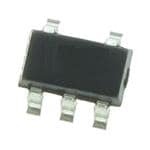
| 描述 | IC REG LDO 3.3V 0.15A SOT23-5低压差稳压器 3.3V 100mA Linear |
| 产品分类 | |
| 品牌 | STMicroelectronics |
| 产品手册 | |
| 产品图片 |
|
| rohs | 符合RoHS无铅 / 符合限制有害物质指令(RoHS)规范要求 |
| 产品系列 | 电源管理 IC,低压差稳压器,STMicroelectronics LK112M33TR- |
| 数据手册 | |
| 产品型号 | LK112M33TR |
| 产品目录页面 | |
| 产品种类 | 低压差稳压器 |
| 供应商器件封装 | SOT-23-5 |
| 其它名称 | 497-7807-1 |
| 其它有关文件 | http://www.st.com/web/catalog/sense_power/FM142/CL1015/SC312/PF63648?referrer=70071840 |
| 包装 | 剪切带 (CT) |
| 商标 | STMicroelectronics |
| 回动电压—最大值 | 350 mV |
| 安装类型 | 表面贴装 |
| 安装风格 | SMD/SMT |
| 封装 | Reel |
| 封装/外壳 | SC-74A,SOT-753 |
| 封装/箱体 | SOT-23-5 |
| 工作温度 | -30°C ~ 125°C |
| 工厂包装数量 | 3000 |
| 最大工作温度 | + 125 C |
| 最大输入电压 | 14 V |
| 最小工作温度 | - 40 C |
| 最小输入电压 | + 3.8 V |
| 标准包装 | 1 |
| 电压-跌落(典型值) | 0.29V @ 150mA |
| 电压-输入 | 最高 16V |
| 电压-输出 | 3.3V |
| 电压调节准确度 | 2 % |
| 电流-输出 | 150mA |
| 电流-限制(最小值) | 150mA |
| 稳压器拓扑 | 正,固定式 |
| 稳压器数 | 1 |
| 系列 | LK112XX33 |
| 线路调整率 | 40 mV |
| 负载调节 | 90 mV |
| 输入偏压电流—最大 | 0.175 mA |
| 输出电压 | 3.3 V |
| 输出电流 | 150 mA |
| 输出端数量 | 1 Output |
| 输出类型 | Fixed |


- 商务部:美国ITC正式对集成电路等产品启动337调查
- 曝三星4nm工艺存在良率问题 高通将骁龙8 Gen1或转产台积电
- 太阳诱电将投资9.5亿元在常州建新厂生产MLCC 预计2023年完工
- 英特尔发布欧洲新工厂建设计划 深化IDM 2.0 战略
- 台积电先进制程称霸业界 有大客户加持明年业绩稳了
- 达到5530亿美元!SIA预计今年全球半导体销售额将创下新高
- 英特尔拟将自动驾驶子公司Mobileye上市 估值或超500亿美元
- 三星加码芯片和SET,合并消费电子和移动部门,撤换高东真等 CEO
- 三星电子宣布重大人事变动 还合并消费电子和移动部门
- 海关总署:前11个月进口集成电路产品价值2.52万亿元 增长14.8%


PDF Datasheet 数据手册内容提取
LK112 Low noise and low drop voltage regulator with shutdown function Datasheet - production data • Internal current and thermal limit • Operative input voltage from: – V + 0.5 to 14 V (for V > 2 V) or from OUT OUT 2.5 V to 14 V (for V < 2 V) OUT Description SOT23-5L The LK112 is a low-dropout linear regulator with a built-in electronic switch. The internal switch can be controlled by TTL or CMOS logic levels. The device is on-state when the control pin is pulled to a logic high level. An external capacitor can be Features connected to the noise bypass pin to reduce the output noise level to 30 µVrms. An internal PNP • Output current up to 150 mA pass transistor is used to achieve a low-dropout • Low-dropout voltage (350 mV at I = 150 voltage. The LK112 has a very low quiescent OUT mA) current in on mode while in off mode Iq is reduced below 100 nA max. The internal thermal • Very low quiescent current: shutdown circuitry limits the junction temperature – 0.1 µA in OFF mode and max. 250 µA in below 150 °C. Load current is internally monitored ON mode at I = 0 mA OUT and the device shuts down in the presence of a • Low output noise: short-circuit or overcurrent condition on the – typ. 30 µV at I = 60 mA and 10 Hz < f < output. OUT 80 kHz • Wide range of output voltages Table 1. Device summary Order codes Output voltages LK112M15TR 1.5V LK112M18TR 1.8V LK112M25TR 2.5V LK112M33TR 3.3V LK112M50TR 5.0V LK112M55TR 5.5V LK112M60TR 6.0V LK112M80TR 8.0V April 2014 DocID7362 Rev 17 1/18 This is information on a product in full production. www.st.com
Contents LK112 Contents 1 Diagram . . . . . . . . . . . . . . . . . . . . . . . . . . . . . . . . . . . . . . . . . . . . . . . . . . . 3 2 Pin configuration . . . . . . . . . . . . . . . . . . . . . . . . . . . . . . . . . . . . . . . . . . . 4 3 Maximum ratings . . . . . . . . . . . . . . . . . . . . . . . . . . . . . . . . . . . . . . . . . . . . 5 4 Electrical characteristics . . . . . . . . . . . . . . . . . . . . . . . . . . . . . . . . . . . . . 6 5 Typical characteristics . . . . . . . . . . . . . . . . . . . . . . . . . . . . . . . . . . . . . . . 7 6 Package mechanical data . . . . . . . . . . . . . . . . . . . . . . . . . . . . . . . . . . . . 13 7 Packaging mechanical data . . . . . . . . . . . . . . . . . . . . . . . . . . . . . . . . . . 15 8 Revision history . . . . . . . . . . . . . . . . . . . . . . . . . . . . . . . . . . . . . . . . . . . 17 2/18 DocID7362 Rev 17
LK112 Diagram 1 Diagram Figure 1. Schematic diagram DocID7362 Rev 17 3/18 18
Pin configuration LK112 2 Pin configuration Figure 2. Pin connection (top view) Table 2. Pin description Pin n° Symbol Note Shutdown input disables the regulator when it is connected to GND or to positive 1 SHDN voltage less than 0.6 V Ground pin internally connected to the die attach flag to decrease the total thermal 2 GND resistance and increase the package ability to dissipate power 3 Bypass Bypass pin with 0.1 µF to improve the noise performance 4 OUT Output port 5 IN Input port 4/18 DocID7362 Rev 17
LK112 Maximum ratings 3 Maximum ratings Table 3. Absolute maximum ratings Symbol Parameter Value Unit V DC input voltage 16 V I V DC input voltage 16 V SHDN I Output current Internally limited O T Storage temperature range -55 to 150 °C STG T Operating junction temperature range -40 to 125 °C OP Table 4. Thermal data Symbol Parameter SOT23-5L Unit R Thermal resistance junction-case 81 °C/W thJC R Thermal resistance junction-ambient 255 °C/W thJA DocID7362 Rev 17 5/18 18
Electrical characteristics LK112 4 Electrical characteristics T = 25 °C, V = V + 1 V, I = 0 mA, V = 1.8 V, C = 1 µF, C = 2.2 µF, J IN OUT OUT SHDN I O C =0.1 µF unless otherwise specified. BYPASS Table 5. LK112 electrical characteristics Symbol Parameter Test conditions Min. Typ. Max. Unit On mode (except I ) 175 250 µA SHDN I Quiescent current q Off mode, V = 8V, V = 0V 0 0.1 µA I SHDN V Output voltage I = 30mA -2 +2 % O O V = V +1V to V +6V, V ≤ 5.6V 0.7 20 mV ΔV Line regulation I O O O O V = V +1V to V +6V, V > 5.6V 0.8 40 mV I O O O I = 1 to 60mA 15 30 mV ΔV Load regulation O O I = 1 to 150mA 25 90 mV O I = 60mA (1) 0.17 0.24 V O V Dropout voltage d I = 150mA (1) 0.29 0.35 V O I Output current limit 150 mA O V = V +1.5V, C = 0.1µF SVR Supply voltage rejection I O BYP 55 dB C = 10µF, f = 400Hz, I = 30mA O O B= 10Hz to 80kHz, C = 0.1µF eN Output noise voltage BYP 30 µVrms C = 10µF, V = V +1.5V, I = 60mA O I O O I Shutdown input current V = 1.8V, output on 12 35 µA SHDN SHDN Output on 1.8 V Shutdown input logic V SHDN Output off 0.6 Output voltage ΔV /T I = 10mA 0.09 mV/°C O J temperature coefficient O 1. For versions with output voltage more than 2.1 V only. Note: For version with output voltage less than 2 V, V = 2.4 V. IN 6/18 DocID7362 Rev 17
LK112 Typical characteristics 5 Typical characteristics Unless otherwise specified, T = 25 °C, C = 1 µF, C = 2.2 µF, C = 100 nF J I O BYP Figure 3. Output voltage vs. temperature (V = 2.5V) Figure 4. Output voltage vs. temperature O (V = 3.8V) O Figure 5. Line regulation vs. temperature Figure 6. Load regulation vs. temperature DocID7362 Rev 17 7/18 18
Typical characteristics LK112 Figure 7. Dropout voltage vs. temperature Figure 8. Short-circuit current vs. dropout voltage Figure 9. Output voltage vs. input voltage Figure 10. Shutdown voltage vs. temperature 2.5 V 2 V 30 mA Figure 11. Shutdown current vs. shutdown Figure 12. Supply voltage rejection vs. voltage temperature (V = 2.5V) O 8/18 DocID7362 Rev 17
LK112 Typical characteristics Figure 13. Supply voltage rejection vs. output Figure 14. Supply voltage rejection vs. current frequency Figure 15. Supply voltage rejection vs. Figure 16. Quiescent current vs. temperature temperature (V = 3.8V) O Figure 17. Quiescent current vs. input voltage Figure 18. Quiescent current vs. shutdown voltage DocID7362 Rev 17 9/18 18
Typical characteristics LK112 Figure 19. Quiescent current vs. output current Figure 20. Reverse current vs. reverse voltage Figure 21. Stability Figure 22. Noise spectrum Figure 23. Start-up transient (C = 10 nF) Figure 24. Start-up transient (C = 100 nF) BYP BYP V=3.5V, V =2.5V, V = 0 to 1.8V, R =2.5kΩ, C=1µF, V=3.5V, V =2.5V, V = 0 to 1.8V, R =68Ω, C=1µF, I O SHDN L I I O SHDN L I C =4.7µF, C =10nF C =4.7µF, C =100nF O BYP O BYP 10/18 DocID7362 Rev 17
LK112 Typical characteristics Figure 25. Line transient (C = 100 µF) Figure 26. Line transient (C = 10 µF) o o V=3.5 to 4.5V, V =2.5V, V = 1.8V, I =30mA, no C, V=3.5 to 4.5V, V =2.5V, V = 1.8V, I =30mA, no C, I O SHDN O I I O SHDN O I C =100µF, C =10nF, t =t=2µs C =10µF, C =10nF, t =t=2µs O BYP s f O BYP s f Figure 27. Line transient (C = 1 µF) Figure 28. Load transient (C = 2.2 µF, o o C =10nF) BYP V=3.5 to 4.5V, V =2.5V, V = 1.8V, I =30mA, no C, V=3.5V, V =2.5V, V = 1.8V, I =50 to 100mA, C=1µF, I O SHDN O I I O SHDN O I C =1µF, C =1nF, t =t=2µs C =2.2µF, C =10nF, t =t=250ns O BYP s f O BYP s f DocID7362 Rev 17 11/18 18
Typical characteristics LK112 Figure 29. Load transient (C = 10 µF, Figure 30. Load transient (V = 3.8 V) o o C =100 nF) BYP V=3.5V, V =2.5V, V = 1.8V, I =50 to 100mA, C=1µF, V=4.8V, V =3.8V, V = 1.8V, I =50 to 100mA, C=1µF, I O SHDN O I I O SHDN O I C =10µF, C =100nF, t =t=250ns C =2.2µF, C =10nF, t =t=250ns O BYP s f O BYP s f 12/18 DocID7362 Rev 17
LK112 Package mechanical data 6 Package mechanical data In order to meet environmental requirements, ST offers these devices in different grades of ECOPACK® packages, depending on their level of environmental compliance. ECOPACK® specifications, grade definitions and product status are available at: www.st.com. ECOPACK® is an ST trademark. Figure 31.SOT23-5L mechanical drawings (cid:26)(cid:26)(cid:19)(cid:19)(cid:23)(cid:23)(cid:28)(cid:28)(cid:25)(cid:25)(cid:26)(cid:26)(cid:25)(cid:25)(cid:66)(cid:66)(cid:78)(cid:78) DocID7362 Rev 17 13/18 18
Package mechanical data LK112 Table 6. SOT23-5L mechanical data mm Dim. Min. Typ. Max. A 0.90 1.45 A1 0 0.15 A2 0.90 1.30 b 0.30 0.50 c 2.09 0.20 D 2.95 E 1.60 e 0.95 H 2.80 L 0.30 0.60 θ 0 8 Figure 32. SOT23-5L recommended footprint (dimensions in mm) (cid:26)(cid:19)(cid:23)(cid:28)(cid:25)(cid:26)(cid:25)(cid:66)(cid:78) 14/18 DocID7362 Rev 17
LK112 Packaging mechanical data 7 Packaging mechanical data Figure 33.Tape and reel SOT23-5L mechanical drawings DocID7362 Rev 17 15/18 18
Packaging mechanical data LK112 Figure 34. Tape and reel SOT23-5L mechanical data mm Dim. Min. Typ. Max. A 180 C 12.8 13.0 13.2 D 20.2 N 60 T 14.4 Ao 3.13 3.23 3.33 Bo 3.07 3.17 3.27 Ko 1.27 1.37 1.47 Po 3.9 4.0 4.1 P 3.9 4.0 4.1 16/18 DocID7362 Rev 17
LK112 Revision history 8 Revision history Table 7. Document revision history Date Revision Changes 31-Jan-2005 8 Change maturity code. 13-Jun-2006 9 Order codes updated and new template. 17-Oct-2006 10 The T value on table 2 has been updated. OP 18-Jul-2007 11 Add Table1 in cover page. 21-Sep-2007 12 Features updated. 11-Dec-2007 13 Modified: Table1. 12-Feb-2008 14 Modified: Table1. 10-Jul-2008 15 Modified: Table1 and Table1 on page1. 28-Feb-2011 16 Modified: Table1. Changed the part number LK112xx to LK112. Updated the Title in cover page and Table1: Device summary. Updated the features and description in cover page, Table2: Pin description, Figure3: Output voltage vs. temperature (VO= 2.5V), 24-Apr-2014 17 Figure4: Output voltage vs. temperature (VO= 3.8V), Section5: Typical characteristics, Section6: Package mechanical data. Added Section7: Packaging mechanical data. Minor text changes. DocID7362 Rev 17 17/18 18
LK112 Please Read Carefully: Information in this document is provided solely in connection with ST products. STMicroelectronics NV and its subsidiaries (“ST”) reserve the right to make changes, corrections, modifications or improvements, to this document, and the products and services described herein at any time, without notice. All ST products are sold pursuant to ST’s terms and conditions of sale. Purchasers are solely responsible for the choice, selection and use of the ST products and services described herein, and ST assumes no liability whatsoever relating to the choice, selection or use of the ST products and services described herein. No license, express or implied, by estoppel or otherwise, to any intellectual property rights is granted under this document. If any part of this document refers to any third party products or services it shall not be deemed a license grant by ST for the use of such third party products or services, or any intellectual property contained therein or considered as a warranty covering the use in any manner whatsoever of such third party products or services or any intellectual property contained therein. UNLESS OTHERWISE SET FORTH IN ST’S TERMS AND CONDITIONS OF SALE ST DISCLAIMS ANY EXPRESS OR IMPLIED WARRANTY WITH RESPECT TO THE USE AND/OR SALE OF ST PRODUCTS INCLUDING WITHOUT LIMITATION IMPLIED WARRANTIES OF MERCHANTABILITY, FITNESS FOR A PARTICULAR PURPOSE (AND THEIR EQUIVALENTS UNDER THE LAWS OF ANY JURISDICTION), OR INFRINGEMENT OF ANY PATENT, COPYRIGHT OR OTHER INTELLECTUAL PROPERTY RIGHT. ST PRODUCTS ARE NOT DESIGNED OR AUTHORIZED FOR USE IN: (A) SAFETY CRITICAL APPLICATIONS SUCH AS LIFE SUPPORTING, ACTIVE IMPLANTED DEVICES OR SYSTEMS WITH PRODUCT FUNCTIONAL SAFETY REQUIREMENTS; (B) AERONAUTIC APPLICATIONS; (C) AUTOMOTIVE APPLICATIONS OR ENVIRONMENTS, AND/OR (D) AEROSPACE APPLICATIONS OR ENVIRONMENTS. WHERE ST PRODUCTS ARE NOT DESIGNED FOR SUCH USE, THE PURCHASER SHALL USE PRODUCTS AT PURCHASER’S SOLE RISK, EVEN IF ST HAS BEEN INFORMED IN WRITING OF SUCH USAGE, UNLESS A PRODUCT IS EXPRESSLY DESIGNATED BY ST AS BEING INTENDED FOR “AUTOMOTIVE, AUTOMOTIVE SAFETY OR MEDICAL” INDUSTRY DOMAINS ACCORDING TO ST PRODUCT DESIGN SPECIFICATIONS. PRODUCTS FORMALLY ESCC, QML OR JAN QUALIFIED ARE DEEMED SUITABLE FOR USE IN AEROSPACE BY THE CORRESPONDING GOVERNMENTAL AGENCY. Resale of ST products with provisions different from the statements and/or technical features set forth in this document shall immediately void any warranty granted by ST for the ST product or service described herein and shall not create or extend in any manner whatsoever, any liability of ST. ST and the ST logo are trademarks or registered trademarks of ST in various countries. Information in this document supersedes and replaces all information previously supplied. The ST logo is a registered trademark of STMicroelectronics. All other names are the property of their respective owners. © 2014 STMicroelectronics - All rights reserved STMicroelectronics group of companies Australia - Belgium - Brazil - Canada - China - Czech Republic - Finland - France - Germany - Hong Kong - India - Israel - Italy - Japan - Malaysia - Malta - Morocco - Philippines - Singapore - Spain - Sweden - Switzerland - United Kingdom - United States of America www.st.com 18/18 DocID7362 Rev 17
Mouser Electronics Authorized Distributor Click to View Pricing, Inventory, Delivery & Lifecycle Information: S TMicroelectronics: LK112M33TR LK112M18TR LK112M15TR LK112M50TR LK112M60TR LK112M25TR LK112M55TR LK112M80TR